EP0051320B1 - Strahlenempfindliches negatives Resistmaterial - Google Patents
Strahlenempfindliches negatives Resistmaterial Download PDFInfo
- Publication number
- EP0051320B1 EP0051320B1 EP81109526A EP81109526A EP0051320B1 EP 0051320 B1 EP0051320 B1 EP 0051320B1 EP 81109526 A EP81109526 A EP 81109526A EP 81109526 A EP81109526 A EP 81109526A EP 0051320 B1 EP0051320 B1 EP 0051320B1
- Authority
- EP
- European Patent Office
- Prior art keywords
- resist
- vinylnaphthalene
- etching
- sensitivity
- p2vn
- Prior art date
- Legal status (The legal status is an assumption and is not a legal conclusion. Google has not performed a legal analysis and makes no representation as to the accuracy of the status listed.)
- Expired
Links
- 229920002120 photoresistant polymer Polymers 0.000 title claims description 12
- 230000005855 radiation Effects 0.000 title claims description 5
- KXYAVSFOJVUIHT-UHFFFAOYSA-N 2-vinylnaphthalene Chemical compound C1=CC=CC2=CC(C=C)=CC=C21 KXYAVSFOJVUIHT-UHFFFAOYSA-N 0.000 claims description 18
- 229920001577 copolymer Polymers 0.000 claims description 17
- 229920000642 polymer Polymers 0.000 claims description 16
- IGGDKDTUCAWDAN-UHFFFAOYSA-N 1-vinylnaphthalene Chemical compound C1=CC=C2C(C=C)=CC=CC2=C1 IGGDKDTUCAWDAN-UHFFFAOYSA-N 0.000 claims description 12
- 239000002861 polymer material Substances 0.000 claims description 10
- IWTYTFSSTWXZFU-UHFFFAOYSA-N 3-chloroprop-1-enylbenzene Chemical compound ClCC=CC1=CC=CC=C1 IWTYTFSSTWXZFU-UHFFFAOYSA-N 0.000 claims description 8
- -1 poly(chloromethyl-2-vinylnaphthalene) Polymers 0.000 claims description 8
- VOZRXNHHFUQHIL-UHFFFAOYSA-N glycidyl methacrylate Chemical compound CC(=C)C(=O)OCC1CO1 VOZRXNHHFUQHIL-UHFFFAOYSA-N 0.000 claims description 5
- 229920001519 homopolymer Polymers 0.000 claims description 5
- SBYMUDUGTIKLCR-UHFFFAOYSA-N 2-chloroethenylbenzene Chemical compound ClC=CC1=CC=CC=C1 SBYMUDUGTIKLCR-UHFFFAOYSA-N 0.000 claims description 3
- 239000000178 monomer Substances 0.000 claims description 3
- 230000035945 sensitivity Effects 0.000 description 29
- 238000005530 etching Methods 0.000 description 28
- 239000000463 material Substances 0.000 description 22
- 238000000034 method Methods 0.000 description 22
- 239000004793 Polystyrene Substances 0.000 description 21
- 229920002223 polystyrene Polymers 0.000 description 19
- 239000000243 solution Substances 0.000 description 18
- 238000001312 dry etching Methods 0.000 description 17
- 239000000758 substrate Substances 0.000 description 16
- 238000011161 development Methods 0.000 description 14
- 238000010894 electron beam technology Methods 0.000 description 12
- LFQSCWFLJHTTHZ-UHFFFAOYSA-N Ethanol Chemical compound CCO LFQSCWFLJHTTHZ-UHFFFAOYSA-N 0.000 description 10
- ZWEHNKRNPOVVGH-UHFFFAOYSA-N 2-Butanone Chemical compound CCC(C)=O ZWEHNKRNPOVVGH-UHFFFAOYSA-N 0.000 description 9
- 239000002904 solvent Substances 0.000 description 9
- WYURNTSHIVDZCO-UHFFFAOYSA-N Tetrahydrofuran Chemical compound C1CCOC1 WYURNTSHIVDZCO-UHFFFAOYSA-N 0.000 description 8
- CTQNGGLPUBDAKN-UHFFFAOYSA-N O-Xylene Chemical compound CC1=CC=CC=C1C CTQNGGLPUBDAKN-UHFFFAOYSA-N 0.000 description 7
- 239000000203 mixture Substances 0.000 description 7
- 239000008096 xylene Substances 0.000 description 7
- OKKJLVBELUTLKV-UHFFFAOYSA-N Methanol Chemical compound OC OKKJLVBELUTLKV-UHFFFAOYSA-N 0.000 description 6
- 238000011156 evaluation Methods 0.000 description 6
- 238000004519 manufacturing process Methods 0.000 description 6
- 238000007265 chloromethylation reaction Methods 0.000 description 5
- 239000007788 liquid Substances 0.000 description 5
- KFZMGEQAYNKOFK-UHFFFAOYSA-N Isopropanol Chemical compound CC(C)O KFZMGEQAYNKOFK-UHFFFAOYSA-N 0.000 description 4
- UFWIBTONFRDIAS-UHFFFAOYSA-N Naphthalene Chemical compound C1=CC=CC2=CC=CC=C21 UFWIBTONFRDIAS-UHFFFAOYSA-N 0.000 description 4
- PPBRXRYQALVLMV-UHFFFAOYSA-N Styrene Chemical compound C=CC1=CC=CC=C1 PPBRXRYQALVLMV-UHFFFAOYSA-N 0.000 description 4
- 238000007334 copolymerization reaction Methods 0.000 description 4
- 125000001997 phenyl group Chemical group [H]C1=C([H])C([H])=C(*)C([H])=C1[H] 0.000 description 4
- 238000010526 radical polymerization reaction Methods 0.000 description 4
- 238000000992 sputter etching Methods 0.000 description 4
- YLQBMQCUIZJEEH-UHFFFAOYSA-N tetrahydrofuran Natural products C=1C=COC=1 YLQBMQCUIZJEEH-UHFFFAOYSA-N 0.000 description 4
- RYHBNJHYFVUHQT-UHFFFAOYSA-N 1,4-Dioxane Chemical compound C1COCCO1 RYHBNJHYFVUHQT-UHFFFAOYSA-N 0.000 description 3
- KTZVZZJJVJQZHV-UHFFFAOYSA-N 1-chloro-4-ethenylbenzene Chemical compound ClC1=CC=C(C=C)C=C1 KTZVZZJJVJQZHV-UHFFFAOYSA-N 0.000 description 3
- UHOVQNZJYSORNB-UHFFFAOYSA-N Benzene Chemical compound C1=CC=CC=C1 UHOVQNZJYSORNB-UHFFFAOYSA-N 0.000 description 3
- VYZAMTAEIAYCRO-UHFFFAOYSA-N Chromium Chemical compound [Cr] VYZAMTAEIAYCRO-UHFFFAOYSA-N 0.000 description 3
- YMWUJEATGCHHMB-UHFFFAOYSA-N Dichloromethane Chemical compound ClCCl YMWUJEATGCHHMB-UHFFFAOYSA-N 0.000 description 3
- 125000004218 chloromethyl group Chemical group [H]C([H])(Cl)* 0.000 description 3
- 229910052804 chromium Inorganic materials 0.000 description 3
- 239000011651 chromium Substances 0.000 description 3
- 238000000921 elemental analysis Methods 0.000 description 3
- 229920003229 poly(methyl methacrylate) Polymers 0.000 description 3
- 239000004926 polymethyl methacrylate Substances 0.000 description 3
- 238000001039 wet etching Methods 0.000 description 3
- OZAIFHULBGXAKX-UHFFFAOYSA-N 2-(2-cyanopropan-2-yldiazenyl)-2-methylpropanenitrile Chemical compound N#CC(C)(C)N=NC(C)(C)C#N OZAIFHULBGXAKX-UHFFFAOYSA-N 0.000 description 2
- 230000001133 acceleration Effects 0.000 description 2
- QUKGYYKBILRGFE-UHFFFAOYSA-N benzyl acetate Chemical compound CC(=O)OCC1=CC=CC=C1 QUKGYYKBILRGFE-UHFFFAOYSA-N 0.000 description 2
- 238000012662 bulk polymerization Methods 0.000 description 2
- XMPZTFVPEKAKFH-UHFFFAOYSA-P ceric ammonium nitrate Chemical compound [NH4+].[NH4+].[Ce+4].[O-][N+]([O-])=O.[O-][N+]([O-])=O.[O-][N+]([O-])=O.[O-][N+]([O-])=O.[O-][N+]([O-])=O.[O-][N+]([O-])=O XMPZTFVPEKAKFH-UHFFFAOYSA-P 0.000 description 2
- 150000001875 compounds Chemical class 0.000 description 2
- 238000001035 drying Methods 0.000 description 2
- 230000002349 favourable effect Effects 0.000 description 2
- 238000005227 gel permeation chromatography Methods 0.000 description 2
- 238000005259 measurement Methods 0.000 description 2
- 125000001624 naphthyl group Chemical group 0.000 description 2
- 229920000620 organic polymer Polymers 0.000 description 2
- WQMWHMMJVJNCAL-UHFFFAOYSA-N 2,4-dimethylpenta-1,4-dien-3-one Chemical compound CC(=C)C(=O)C(C)=C WQMWHMMJVJNCAL-UHFFFAOYSA-N 0.000 description 1
- IOEJWYQRSYIWOJ-UHFFFAOYSA-N 2-(chloromethyl)-1-ethenylnaphthalene Chemical compound C1=CC=CC2=C(C=C)C(CCl)=CC=C21 IOEJWYQRSYIWOJ-UHFFFAOYSA-N 0.000 description 1
- ZAMOUSCENKQFHK-UHFFFAOYSA-N Chlorine atom Chemical compound [Cl] ZAMOUSCENKQFHK-UHFFFAOYSA-N 0.000 description 1
- JIGUQPWFLRLWPJ-UHFFFAOYSA-N Ethyl acrylate Chemical compound CCOC(=O)C=C JIGUQPWFLRLWPJ-UHFFFAOYSA-N 0.000 description 1
- 238000005727 Friedel-Crafts reaction Methods 0.000 description 1
- 239000005062 Polybutadiene Substances 0.000 description 1
- 238000000862 absorption spectrum Methods 0.000 description 1
- HEZJLLQLTPQSMT-UHFFFAOYSA-N acetic acid;1,2-diphenylethane-1,2-dione Chemical compound CC(O)=O.C=1C=CC=CC=1C(=O)C(=O)C1=CC=CC=C1 HEZJLLQLTPQSMT-UHFFFAOYSA-N 0.000 description 1
- 239000007864 aqueous solution Substances 0.000 description 1
- 229940007550 benzyl acetate Drugs 0.000 description 1
- 230000015572 biosynthetic process Effects 0.000 description 1
- HRQGCQVOJVTVLU-UHFFFAOYSA-N bis(chloromethyl) ether Chemical compound ClCOCCl HRQGCQVOJVTVLU-UHFFFAOYSA-N 0.000 description 1
- 239000003153 chemical reaction reagent Substances 0.000 description 1
- 229910052801 chlorine Inorganic materials 0.000 description 1
- 239000000460 chlorine Substances 0.000 description 1
- 230000007423 decrease Effects 0.000 description 1
- 230000001419 dependent effect Effects 0.000 description 1
- 238000007865 diluting Methods 0.000 description 1
- 238000009826 distribution Methods 0.000 description 1
- 230000005670 electromagnetic radiation Effects 0.000 description 1
- 238000007720 emulsion polymerization reaction Methods 0.000 description 1
- 238000005516 engineering process Methods 0.000 description 1
- 238000001914 filtration Methods 0.000 description 1
- 239000003999 initiator Substances 0.000 description 1
- 238000010884 ion-beam technique Methods 0.000 description 1
- 150000002500 ions Chemical class 0.000 description 1
- 230000015654 memory Effects 0.000 description 1
- 238000012986 modification Methods 0.000 description 1
- 230000004048 modification Effects 0.000 description 1
- 238000000059 patterning Methods 0.000 description 1
- PNJWIWWMYCMZRO-UHFFFAOYSA-N pent‐4‐en‐2‐one Natural products CC(=O)CC=C PNJWIWWMYCMZRO-UHFFFAOYSA-N 0.000 description 1
- 238000000206 photolithography Methods 0.000 description 1
- 238000001020 plasma etching Methods 0.000 description 1
- 229920002454 poly(glycidyl methacrylate) polymer Polymers 0.000 description 1
- 229920002857 polybutadiene Polymers 0.000 description 1
- 230000000379 polymerizing effect Effects 0.000 description 1
- 239000011148 porous material Substances 0.000 description 1
- 238000001556 precipitation Methods 0.000 description 1
- 238000007670 refining Methods 0.000 description 1
- 239000004065 semiconductor Substances 0.000 description 1
- 150000003440 styrenes Chemical class 0.000 description 1
- 239000000126 substance Substances 0.000 description 1
- 230000008961 swelling Effects 0.000 description 1
- 238000003786 synthesis reaction Methods 0.000 description 1
- 238000010189 synthetic method Methods 0.000 description 1
- 238000012360 testing method Methods 0.000 description 1
Images

Classifications
-
- G—PHYSICS
- G03—PHOTOGRAPHY; CINEMATOGRAPHY; ANALOGOUS TECHNIQUES USING WAVES OTHER THAN OPTICAL WAVES; ELECTROGRAPHY; HOLOGRAPHY
- G03F—PHOTOMECHANICAL PRODUCTION OF TEXTURED OR PATTERNED SURFACES, e.g. FOR PRINTING, FOR PROCESSING OF SEMICONDUCTOR DEVICES; MATERIALS THEREFOR; ORIGINALS THEREFOR; APPARATUS SPECIALLY ADAPTED THEREFOR
- G03F7/00—Photomechanical, e.g. photolithographic, production of textured or patterned surfaces, e.g. printing surfaces; Materials therefor, e.g. comprising photoresists; Apparatus specially adapted therefor
- G03F7/004—Photosensitive materials
- G03F7/038—Macromolecular compounds which are rendered insoluble or differentially wettable
Definitions
- the present invention relates to a negative resist of the type which contains a polymer material sensitive to radiant rays (such as an electron beam, an X-ray, a y-ray, and other short wavelength electromagnetic radiation), or corpuscular beams (such as an ion beam and a neutron beam).
- radiant rays such as an electron beam, an X-ray, a y-ray, and other short wavelength electromagnetic radiation
- corpuscular beams such as an ion beam and a neutron beam
- Fine fabrication of integrated circuits, bubble memories and the like have customarily been done by the technique of photolithography in which a photosensitive material is subjected to light irradiation to form a desired resist pattern.
- a finer pattern fabrication technique using a deep ultraviolet ray, an X-ray, an electron beam or like radiation has been recently developed for practical use.
- resists are classified into two different types, i.e., a positive type and a negative type.
- a positive type resist becomes easily soluble in a solvent when subjected to irradiation; irradiated portions will be dissolved and removed by the subsequent development, while non-irradiated portions will remain unremoved to form a pattern.
- a negative type resist becomes non-soluble or sparingly soluble in a solvent when irradiated; irradiated portions will remain unremoved after development to form a pattern with non-irradiated portions removed.
- an image identical to the irradiation pattern or opposite thereto will be formed depending on the type of a resist used.
- poly(glycidyl methacrylate), copolymer of glycidyl methacrylate and ethyl acrylate, epoxidized polybutadiene, and poly(diallyl-o-phthalate) are well known.
- the resistance must be ensured to an aqueous solution of ceric ammonium nitrate which is an etching solution for chromium.
- ceric ammonium nitrate which is an etching solution for chromium.
- etching a resist by a dry etching process which may employ a beam or shower of ions or plasma. This is employed to promote an anisotropic etching process, in place of a wet etching process which is isotropic, that ensures a desired precision in circuit fabrication. Also, it is employed in circuit fabrication to realize a maskless step in which delineation is applied directly to a substrate. Unless the resist which protects the substrate against the beam or shower in these applications is sufficiently resistive to dry etching, the bared and protected surface regions on the substrate would become indistinct from each other. Accordingly, the resistance should favorably be as large as possible so that a dry etching process can be performed with high accuracy.
- the invention provides a dry-etchable radiation-sensitive negative resist consisting of a polymer material which contains at least one polymer selected from homopolymers of 1- or 2-vinylnaphthalene, chloromethyl-1- or 2-vinylnaphthalene and copolymers wherein the moiety of vinylnaphthalene is equal to or greater than 50 percent in terms of monomeric unit ratio.
- the resolution of a resist itself might be deteriorated in the event of development. It is preferred therefore to use a solvent which can dissolve and remove non-irradiated portions of the resist without causing the irradiated portions of the resist to swell. This is particularly true for those polymers which have larger molecular weights within the specific range defined as above.
- a molecular weight and a copolymerization ratio can be chosen suitably in accordance with a desired sensitivity and process characteristics.
- a negative resist proposed by the present invention has resistance to dry etching which is far higher than that of all the organic resists known in the art. Use of such a material in the fabrication of semiconductors, integrated circuits or the like will ensure a safe etching step.
- a resist according to the invention needs only a minimum of thickness on a substrate due to the improved etching resistance.
- a thick resist film on a substrate degrades the resolution when subjected to electron beam irradiation, for example, because electrons driven into the resist will be scattered in all directions therein.
- a negative resist sensitive to a radiant ray or a corpuscular beam which comprises a polymer material wherein the polymer material contains at least one composition chosen from the group of:
- Poly-2-vinylnaphthalene (P2VN) provided by bulk polymerization was subjected to fractional precipitation to prepare a sample with dioxane employed as a solvent and ethanol as a non-solvent. A molecular weight distribution of the sample was measured by gel permeation chromatography.
- a resist solution was prepared by dissolving in dioxane 10 weight percent of the sample whose weight average molecular weight was 120,000 and polydispersivity was 1.6.
- the resist solution was spin-coated at 2,500 rpm (revolutions per minute) onto a substrate followed by prebaking at 100°C (degrees centrigrade) for 30 minutes to obtain a uniform film of about 0.7 micrometer ( ⁇ m) in thickness.
- various kinds of pattern delineation were applied using an electron beam exposure system (available from Japan Electron Optics Laboratory under the trade name JBX-5A) at an acceleration voltage of 20 KV (kilovolts) and with different doses.
- the substrate was taken out from the exposure system and dipped for 60 seconds in a liquid containing 4 parts of tetrahydrofuran and 1 part of ethanol for development, and was rinsed in a liquid containing 1 part of methyl ethyl ketone and 1 part of ethanol for 30 seconds to obtain resist patterns on the substrate.
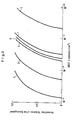
- film thicknesses were measured by a product available from Rank Taylor Hobson under the trade name Taly step to determine the relationship between the residual film thickness and the dose. The measurement resulted a sensitivity curve 1 shown in Figure 1.
- a dose Dg.
- P2VN was prepared in the same way as in Example 1 except that the sample had an average molecular weight of 190,000.
- a resist solution was prepared by dissolving the sample in xylene by 3 weight percent. The solution was spin-coated onto a substrate at 2,500 rpm and prebaked at 100°C for 30 minutes to obtain a uniform film of about 0.3 um.
- Poly-1-vinylnaphthalene.(P1VN) prepared by radical polymerization was allowed for evaluation as in Example 1.
- etching rates indicated in Table 1 are average etching rates measured by etching the materials each for 10 minutes at 2.67.10-2 Pa (2 x 10- 4 Torr) employing an instrument under the trade name three- inch Microetch system available from Veeco Company.
- PMMA poly methyl methacrylate
- AZ-1350J a product available from Shipley Company under the trade name AZ-1350J
- PM1PK poly isopropenyl ketone
- PS polystyrene
- polystyrene has been known as an organic polymer resist whose etching rate is considerably low
- the materials P1 VN and P2VN show etching rates for lower than that of polystyrene, that is, about two-thirds of polystyrene, as will be seen from Table 1.
- Table 2 represents etching rates for conventional AZ and PS and those for P2VN under several etching techniques.
- Polystyrene for example, undergoes a variation in etching rate which is as little as several percent or less for molecular weights of 3,000 up to 1 million.
- a suitable method for the synthesis of P2VN is ordinary radical polymerization when the molecular weight is less than 100,000, bulk polymerization when it is of the order of 100,000-300,000 or emulsion polymerization when it is more than 500,000.
- P1VN and P2VN are commercially available as reagents, they are not usable as resists unless refined. Synthetic methods of P2VN are well known, and for example, for details of the radical polymerization, reference is made to US-A-1,982,676.
- chloromethylation can be adopted for polystyrene for the purpose of increasing the sensitivity of a resist.
- chloromethylation of P2VN proceeds far faster than polystyrene and might cause gelling of the material if performed carelessly. Thus, one must be precautious enough to avoid this such as by diluting the solution to a sufficient degree.
- a copolymer of chloromethyl styrene and 2-vinylnaphthalene is readily obtainable by ordinary radical polymerization.
- a monomeric mixture containing 0.01 mole 2-vinylnaphthalene and 0.02 mole chloromethyl styrene (consisting of 60% m-chloromethyl and 40% p-chlorostyrene) was added with AIBN (azobisisobutylonitrile) of 1 mole percent to the monomer concentration as an initiator.
- AIBN azobisisobutylonitrile
- the mixture was dissolved in 20 milliliters of refined benzene.
- the mixture solution was poured in a polymerizing tube, freeze-deaerated and polymerized in the sealed tube at 70°C for 24 hours.
- the solution was then introduced into 100 milliliters of methanol to separate a polymer.
- the polymer was purified by reprecipation, using methylene chloride, and methanol as solvent and non-solvent, respectively. After being repeatedly subjected to such a refining process three times, the polymers were dried under reduced pressure. A copolymerization ratio was determined from the elemental analysis of the resultant polymers (chlorine content).
- a sensitivity curve 1 in Figure 2 the abscissa indicates the dose and the ordinate, the film thickness after development normalized by the thickness before development.
- Evaluation of the resist solution by the same method as in Example 5 provided a sensitivity curve 3 shown in Figure 2.
- the substrate was dipped in a mixture liquid containing 3 part of tetrahydrofuran and 1 part of ethanol for development for 60 seconds followed by rinsing in isopropanol.
- the gel point dose was 5.0 x 10- 6 C/cm 2 while D 0.5 g was 8 x 10- 4 C/cm 2 . It was also the case with this Example that patterns less than 1 pm were sufficiently resolved.
- a copolymer was produced from a 10:2 mixture of 2-vinylnaphthalene and p-chlorostyrene using the same radical copolymerization process as in Example 5.
- the solution was filtered through a 0.2 ⁇ m filter to prepare a resist solution. This solution was spin-coated onto a substrate at 2000 rpm and prebaked at 100°C for 30 minutes to obtain a uniform film of about 0.2 ⁇ m in thickness.
- Example 5 The same evaluation as in Example 5 was performed for this product to obtain a sensitivity curve 4 shown in Figure 2.
- a dose (D 0.5 g ) which provides a film of one half of the initial thickness was 3.5 x 10- 4 C/cm 2.
- the sensitivity was found to be twice the sensitivity for P2VN. Resist patterns less than 1 ⁇ m were fully resolved.
- Example 5 The evaluation was performed as in Example 5.
- the sensitivity curve for the resultant resist is shown in Figure 2.
- the substrate was dipped for 60 seconds in a liquid containing 3 part of tetrahydrofuran and 1 part of methyl ethyl ketone for development followed by rinsing in a liquid 1 part of methyl ethyl ketone and 2 part of ethanol for 30 seconds.
- a gel point dose (D i g ) was 2.3 x 10- 5 C/cm 2 while (D 0.5 g ) was 3.6 ⁇ 10 -5 C/cm2.
- a copolymer of 2-vinylnaphthalene and glycidyl methacrylate provided by radical copolymerization was allowed for evaluation as a resist.
- the monomeric unit ratio between 2-vinylnaphthalene and glycidyl methacrylate ratio was determined to be about 85:15 by elemental analysis and infrared absorption spectrum, although the monomer ratio of charge was to be 50:50.
- the weight average molecular weight was 260,000 and the polydispersivity 1.9, as measured by gel permeation chromatography.
- a sensitivity curve representing this case is indicated by the reference numeral 6 in Figure 2.
- Examples 4 and 5 to 10 indicated examples of chloromethylated compounds of P2VN and copolymers containing 2-vinylnaphthalene. What is of utmost concern here is whether such materials are poorer in etching resistance than homopolymers of 2-vinylnaphthalene.
- Measurement of etching rates under an Ar ion milling etching technique as stated in connection with Table 1 proved that the etching rate increased by the order of 20% compared to P2VN when about 20% chloromethyl styrene, chlorostyrene or glycidyl methacrylate is copolymerized with the materials concerned.
- Chloromethylation is also effective to increase the etching rate though insignificant (10 to 20%). In any case, however, etching rates obtainable with such materials are lower than that of polystyrene.
- etching rates for polystyrene, chloromethylated polystyrene, P2VN, chloromethylated P2VN, and poly(chloromethyl styrene-CO-2-vinyl- naphtalene) were measured to be 22, 26,15,18, and 18.5 nm/min, respectively.
- etching rate of two-thirds implies that the thickness of a resist film employed in a dry etching step may be two-thirds.
- a thick resist film deteriorates the resolution in electron beam irradiation due to scattering of the electrons. In other words, the thinner the film is, the higher the resolution grows.
- the homopolymer, or P2VN is desirable when a negative resist of the greatest resistance to dry etching is needed.
- a desirable material will be a chloromethylated compound of P2VN.
- the molecular weight of a material used should be as large as possible in view of the fact that the weight average molecular weight M w and necessary dose for patterning are inversely proportional to each other.
- materials of large molecular weights swell during development and thereby deteriorate the resolution. It follows that materials of small molecular weights must be employed if resolution has priority to the other factors.
Landscapes
- Physics & Mathematics (AREA)
- Spectroscopy & Molecular Physics (AREA)
- General Physics & Mathematics (AREA)
- Materials For Photolithography (AREA)
- Exposure And Positioning Against Photoresist Photosensitive Materials (AREA)
Claims (3)
Applications Claiming Priority (6)
| Application Number | Priority Date | Filing Date | Title |
|---|---|---|---|
| JP15535180A JPS5778529A (en) | 1980-11-05 | 1980-11-05 | Resist material |
| JP155351/80 | 1980-11-05 | ||
| JP56078967A JPS57192947A (en) | 1981-05-25 | 1981-05-25 | Resist material |
| JP7896881A JPS57192948A (en) | 1981-05-25 | 1981-05-25 | Resist material |
| JP78968/81 | 1981-05-25 | ||
| JP78967/81 | 1981-05-25 |
Publications (3)
| Publication Number | Publication Date |
|---|---|
| EP0051320A2 EP0051320A2 (de) | 1982-05-12 |
| EP0051320A3 EP0051320A3 (en) | 1983-01-19 |
| EP0051320B1 true EP0051320B1 (de) | 1986-06-04 |
Family
ID=27302868
Family Applications (1)
| Application Number | Title | Priority Date | Filing Date |
|---|---|---|---|
| EP81109526A Expired EP0051320B1 (de) | 1980-11-05 | 1981-11-05 | Strahlenempfindliches negatives Resistmaterial |
Country Status (3)
| Country | Link |
|---|---|
| US (1) | US4592993A (de) |
| EP (1) | EP0051320B1 (de) |
| DE (1) | DE3174780D1 (de) |
Families Citing this family (5)
| Publication number | Priority date | Publication date | Assignee | Title |
|---|---|---|---|---|
| DE3319558C2 (de) * | 1982-05-31 | 1986-10-30 | Kureha Kagaku Kogyo K.K., Nihonbashi, Tokio/Tokyo | Strahlungsempfindliches Gemisch |
| US5270116A (en) * | 1986-07-10 | 1993-12-14 | Minnesota Mining And Manufacturing Company | Process for fluorimetric monitoring of functional coatings and compositions and fluorescent agents therefor |
| JP2694097B2 (ja) * | 1992-03-03 | 1997-12-24 | インターナショナル・ビジネス・マシーンズ・コーポレイション | 反射防止コーティング組成物 |
| WO2006096221A1 (en) * | 2004-12-16 | 2006-09-14 | International Business Machines Corporation | Low refractive index polymers as underlayers for silicon-containing photoresists |
| US7326523B2 (en) * | 2004-12-16 | 2008-02-05 | International Business Machines Corporation | Low refractive index polymers as underlayers for silicon-containing photoresists |
Family Cites Families (8)
| Publication number | Priority date | Publication date | Assignee | Title |
|---|---|---|---|---|
| US3164575A (en) * | 1958-06-18 | 1965-01-05 | Union Carbide Corp | Polymers of alkenyl naphthalene and method of making same |
| NL131028C (de) * | 1959-06-25 | |||
| US3357831A (en) * | 1965-06-21 | 1967-12-12 | Harris Intertype Corp | Photopolymer |
| US3825430A (en) * | 1972-02-09 | 1974-07-23 | Minnesota Mining & Mfg | Light-sensitive composition and method |
| US3817957A (en) * | 1972-03-24 | 1974-06-18 | Phillips Petroleum Co | Promoters in the treatment of polymerization mixtures with halogenated polymerizable compounds |
| US3885963A (en) * | 1972-04-18 | 1975-05-27 | Xerox Corp | Light activating imaging process |
| US4208211A (en) * | 1978-05-23 | 1980-06-17 | Bell Telephone Laboratories, Incorporated | Fabrication based on radiation sensitive resists and related products |
| US4201580A (en) * | 1978-07-24 | 1980-05-06 | Bell Telephone Laboratories, Incorporated | Lithographic fabrication with treatment of "living polymer" |
-
1981
- 1981-11-05 DE DE8181109526T patent/DE3174780D1/de not_active Expired
- 1981-11-05 EP EP81109526A patent/EP0051320B1/de not_active Expired
-
1985
- 1985-10-15 US US06/787,695 patent/US4592993A/en not_active Expired - Lifetime
Also Published As
| Publication number | Publication date |
|---|---|
| DE3174780D1 (en) | 1986-07-10 |
| US4592993A (en) | 1986-06-03 |
| EP0051320A2 (de) | 1982-05-12 |
| EP0051320A3 (en) | 1983-01-19 |
Similar Documents
| Publication | Publication Date | Title |
|---|---|---|
| Haller et al. | High-resolution positive resists for electron-beam exposure | |
| US4722881A (en) | Radiation-sensitive resist composition with an admixture of cis-(1,3,5,7-tetrahydroxy)-1,3,5,7-tetraphenylcyclotetrasiloxane and a polysilsesquioxane | |
| US4507384A (en) | Pattern forming material and method for forming pattern therewith | |
| US4061829A (en) | Negative resist for X-ray and electron beam lithography and method of using same | |
| US4024293A (en) | High sensitivity resist system for lift-off metallization | |
| EP0192078B1 (de) | Verfahren zur Herstellung von negativen Reliefbildern | |
| EP0067066B2 (de) | Trocken entwickelbare Resistzusammensetzung | |
| CA1166061A (en) | Method of forming a negative resist pattern by exposing to crosslink a copolymer containing halomethyl or acrylymethyl substituted styrene units | |
| EP0051320B1 (de) | Strahlenempfindliches negatives Resistmaterial | |
| US4612270A (en) | Two-layer negative resist | |
| US4965340A (en) | Copolymer from sulfur dioxide and vinyl compound | |
| US4367281A (en) | Fine fabrication process using radiation sensitive resist | |
| US4415653A (en) | Method of making sensitive positive electron beam resists | |
| EP0064864B1 (de) | Verfahren zur Herstellung von empfindlichen positiven Elektronenstrahlresists | |
| JPS58207041A (ja) | 放射線感応性高分子レジスト | |
| JPS62240953A (ja) | レジスト | |
| US4233394A (en) | Method of patterning a substrate | |
| JPH0330852B2 (de) | ||
| JPS647375B2 (de) | ||
| US4504631A (en) | Photoresist material | |
| JPH0547098B2 (de) | ||
| JPH05257285A (ja) | 放射線感光材料およびそれを用いるパターン形成方法 | |
| JPS647651B2 (de) | ||
| JPH033214B2 (de) | ||
| JPS6260691B2 (de) |
Legal Events
| Date | Code | Title | Description |
|---|---|---|---|
| PUAI | Public reference made under article 153(3) epc to a published international application that has entered the european phase |
Free format text: ORIGINAL CODE: 0009012 |
|
| AK | Designated contracting states |
Designated state(s): DE FR GB NL |
|
| PUAL | Search report despatched |
Free format text: ORIGINAL CODE: 0009013 |
|
| AK | Designated contracting states |
Designated state(s): DE FR GB NL |
|
| 17P | Request for examination filed |
Effective date: 19830126 |
|
| RAP1 | Party data changed (applicant data changed or rights of an application transferred) |
Owner name: NEC CORPORATION |
|
| GRAA | (expected) grant |
Free format text: ORIGINAL CODE: 0009210 |
|
| AK | Designated contracting states |
Kind code of ref document: B1 Designated state(s): DE FR GB NL |
|
| REF | Corresponds to: |
Ref document number: 3174780 Country of ref document: DE Date of ref document: 19860710 |
|
| ET | Fr: translation filed | ||
| PLBE | No opposition filed within time limit |
Free format text: ORIGINAL CODE: 0009261 |
|
| STAA | Information on the status of an ep patent application or granted ep patent |
Free format text: STATUS: NO OPPOSITION FILED WITHIN TIME LIMIT |
|
| 26N | No opposition filed | ||
| PGFP | Annual fee paid to national office [announced via postgrant information from national office to epo] |
Ref country code: GB Payment date: 19911031 Year of fee payment: 11 |
|
| PGFP | Annual fee paid to national office [announced via postgrant information from national office to epo] |
Ref country code: FR Payment date: 19911125 Year of fee payment: 11 |
|
| PGFP | Annual fee paid to national office [announced via postgrant information from national office to epo] |
Ref country code: NL Payment date: 19911130 Year of fee payment: 11 |
|
| PGFP | Annual fee paid to national office [announced via postgrant information from national office to epo] |
Ref country code: DE Payment date: 19920123 Year of fee payment: 11 |
|
| PG25 | Lapsed in a contracting state [announced via postgrant information from national office to epo] |
Ref country code: GB Effective date: 19921105 |
|
| PG25 | Lapsed in a contracting state [announced via postgrant information from national office to epo] |
Ref country code: NL Effective date: 19930601 |
|
| GBPC | Gb: european patent ceased through non-payment of renewal fee |
Effective date: 19921105 |
|
| NLV4 | Nl: lapsed or anulled due to non-payment of the annual fee | ||
| PG25 | Lapsed in a contracting state [announced via postgrant information from national office to epo] |
Ref country code: FR Effective date: 19930730 |
|
| PG25 | Lapsed in a contracting state [announced via postgrant information from national office to epo] |
Ref country code: DE Effective date: 19930803 |
|
| REG | Reference to a national code |
Ref country code: FR Ref legal event code: ST |