EP0051249A2 - Process for forming epitaxially extended polycrystalline structures - Google Patents
Process for forming epitaxially extended polycrystalline structures Download PDFInfo
- Publication number
- EP0051249A2 EP0051249A2 EP81108974A EP81108974A EP0051249A2 EP 0051249 A2 EP0051249 A2 EP 0051249A2 EP 81108974 A EP81108974 A EP 81108974A EP 81108974 A EP81108974 A EP 81108974A EP 0051249 A2 EP0051249 A2 EP 0051249A2
- Authority
- EP
- European Patent Office
- Prior art keywords
- layer
- polycrystalline
- silicon
- silicon layer
- temperature
- Prior art date
- Legal status (The legal status is an assumption and is not a legal conclusion. Google has not performed a legal analysis and makes no representation as to the accuracy of the status listed.)
- Granted
Links
- 238000000034 method Methods 0.000 title claims abstract description 20
- 230000008569 process Effects 0.000 title abstract description 9
- 229910021420 polycrystalline silicon Inorganic materials 0.000 claims abstract description 53
- XUIMIQQOPSSXEZ-UHFFFAOYSA-N Silicon Chemical compound [Si] XUIMIQQOPSSXEZ-UHFFFAOYSA-N 0.000 claims abstract description 34
- 229910052710 silicon Inorganic materials 0.000 claims abstract description 28
- 239000010703 silicon Substances 0.000 claims abstract description 28
- 229910021417 amorphous silicon Inorganic materials 0.000 claims abstract description 20
- 239000013078 crystal Substances 0.000 claims abstract description 12
- 238000000151 deposition Methods 0.000 claims description 15
- 239000000758 substrate Substances 0.000 claims description 14
- VYPSYNLAJGMNEJ-UHFFFAOYSA-N Silicium dioxide Chemical compound O=[Si]=O VYPSYNLAJGMNEJ-UHFFFAOYSA-N 0.000 claims description 13
- 239000012212 insulator Substances 0.000 claims description 10
- 238000010438 heat treatment Methods 0.000 claims description 5
- 235000012239 silicon dioxide Nutrition 0.000 claims description 4
- 239000000377 silicon dioxide Substances 0.000 claims description 4
- 229910021421 monocrystalline silicon Inorganic materials 0.000 claims description 3
- 239000012535 impurity Substances 0.000 claims description 2
- 239000002184 metal Substances 0.000 claims description 2
- 229910052814 silicon oxide Inorganic materials 0.000 claims description 2
- 239000011248 coating agent Substances 0.000 claims 9
- 238000000576 coating method Methods 0.000 claims 9
- AHKZTVQIVOEVFO-UHFFFAOYSA-N oxide(2-) Chemical compound [O-2] AHKZTVQIVOEVFO-UHFFFAOYSA-N 0.000 claims 1
- 229920005591 polysilicon Polymers 0.000 abstract description 38
- 238000000137 annealing Methods 0.000 abstract description 3
- 230000015572 biosynthetic process Effects 0.000 abstract description 3
- 239000000463 material Substances 0.000 abstract description 2
- 239000010410 layer Substances 0.000 description 48
- 230000008021 deposition Effects 0.000 description 12
- 238000005516 engineering process Methods 0.000 description 7
- 238000004519 manufacturing process Methods 0.000 description 7
- 238000003917 TEM image Methods 0.000 description 6
- 238000002425 crystallisation Methods 0.000 description 5
- 230000008025 crystallization Effects 0.000 description 5
- 239000004065 semiconductor Substances 0.000 description 4
- BLRPTPMANUNPDV-UHFFFAOYSA-N Silane Chemical group [SiH4] BLRPTPMANUNPDV-UHFFFAOYSA-N 0.000 description 3
- 238000010276 construction Methods 0.000 description 3
- 230000015654 memory Effects 0.000 description 3
- 238000001465 metallisation Methods 0.000 description 3
- 239000005360 phosphosilicate glass Substances 0.000 description 3
- 229910000077 silane Inorganic materials 0.000 description 3
- 239000011800 void material Substances 0.000 description 3
- KRHYYFGTRYWZRS-UHFFFAOYSA-N Fluorane Chemical compound F KRHYYFGTRYWZRS-UHFFFAOYSA-N 0.000 description 2
- QVGXLLKOCUKJST-UHFFFAOYSA-N atomic oxygen Chemical compound [O] QVGXLLKOCUKJST-UHFFFAOYSA-N 0.000 description 2
- 230000015556 catabolic process Effects 0.000 description 2
- 238000001444 catalytic combustion detection Methods 0.000 description 2
- 229910021419 crystalline silicon Inorganic materials 0.000 description 2
- 238000000354 decomposition reaction Methods 0.000 description 2
- 238000009792 diffusion process Methods 0.000 description 2
- 238000011065 in-situ storage Methods 0.000 description 2
- 230000007246 mechanism Effects 0.000 description 2
- 230000003647 oxidation Effects 0.000 description 2
- 238000007254 oxidation reaction Methods 0.000 description 2
- 239000001301 oxygen Substances 0.000 description 2
- 229910052760 oxygen Inorganic materials 0.000 description 2
- GICIECWTEWJCRE-UHFFFAOYSA-N 3,4,4,7-tetramethyl-2,3-dihydro-1h-naphthalene Chemical compound CC1=CC=C2C(C)(C)C(C)CCC2=C1 GICIECWTEWJCRE-UHFFFAOYSA-N 0.000 description 1
- 235000010627 Phaseolus vulgaris Nutrition 0.000 description 1
- 244000046052 Phaseolus vulgaris Species 0.000 description 1
- 239000012159 carrier gas Substances 0.000 description 1
- 230000008859 change Effects 0.000 description 1
- 238000005229 chemical vapour deposition Methods 0.000 description 1
- 230000008602 contraction Effects 0.000 description 1
- 230000007547 defect Effects 0.000 description 1
- 238000006731 degradation reaction Methods 0.000 description 1
- 238000005530 etching Methods 0.000 description 1
- BHEPBYXIRTUNPN-UHFFFAOYSA-N hydridophosphorus(.) (triplet) Chemical compound [PH] BHEPBYXIRTUNPN-UHFFFAOYSA-N 0.000 description 1
- 238000009413 insulation Methods 0.000 description 1
- 239000011229 interlayer Substances 0.000 description 1
- 238000002955 isolation Methods 0.000 description 1
- 238000012986 modification Methods 0.000 description 1
- 230000004048 modification Effects 0.000 description 1
- 230000006911 nucleation Effects 0.000 description 1
- 238000010899 nucleation Methods 0.000 description 1
- 230000001590 oxidative effect Effects 0.000 description 1
- 230000009467 reduction Effects 0.000 description 1
- LIVNPJMFVYWSIS-UHFFFAOYSA-N silicon monoxide Chemical class [Si-]#[O+] LIVNPJMFVYWSIS-UHFFFAOYSA-N 0.000 description 1
- 239000007787 solid Substances 0.000 description 1
- 238000005979 thermal decomposition reaction Methods 0.000 description 1
- 238000013169 thromboelastometry Methods 0.000 description 1
- 238000004627 transmission electron microscopy Methods 0.000 description 1
Images


Classifications
-
- H—ELECTRICITY
- H01—ELECTRIC ELEMENTS
- H01L—SEMICONDUCTOR DEVICES NOT COVERED BY CLASS H10
- H01L21/00—Processes or apparatus adapted for the manufacture or treatment of semiconductor or solid state devices or of parts thereof
- H01L21/02—Manufacture or treatment of semiconductor devices or of parts thereof
- H01L21/02104—Forming layers
- H01L21/02365—Forming inorganic semiconducting materials on a substrate
- H01L21/02656—Special treatments
- H01L21/02664—Aftertreatments
- H01L21/02667—Crystallisation or recrystallisation of non-monocrystalline semiconductor materials, e.g. regrowth
-
- H—ELECTRICITY
- H01—ELECTRIC ELEMENTS
- H01L—SEMICONDUCTOR DEVICES NOT COVERED BY CLASS H10
- H01L21/00—Processes or apparatus adapted for the manufacture or treatment of semiconductor or solid state devices or of parts thereof
- H01L21/02—Manufacture or treatment of semiconductor devices or of parts thereof
- H01L21/02104—Forming layers
- H01L21/02365—Forming inorganic semiconducting materials on a substrate
- H01L21/02436—Intermediate layers between substrates and deposited layers
- H01L21/02439—Materials
- H01L21/02441—Group 14 semiconducting materials
- H01L21/0245—Silicon, silicon germanium, germanium
-
- H—ELECTRICITY
- H01—ELECTRIC ELEMENTS
- H01L—SEMICONDUCTOR DEVICES NOT COVERED BY CLASS H10
- H01L21/00—Processes or apparatus adapted for the manufacture or treatment of semiconductor or solid state devices or of parts thereof
- H01L21/02—Manufacture or treatment of semiconductor devices or of parts thereof
- H01L21/02104—Forming layers
- H01L21/02365—Forming inorganic semiconducting materials on a substrate
- H01L21/02518—Deposited layers
- H01L21/02521—Materials
- H01L21/02524—Group 14 semiconducting materials
- H01L21/02532—Silicon, silicon germanium, germanium
-
- H—ELECTRICITY
- H01—ELECTRIC ELEMENTS
- H01L—SEMICONDUCTOR DEVICES NOT COVERED BY CLASS H10
- H01L21/00—Processes or apparatus adapted for the manufacture or treatment of semiconductor or solid state devices or of parts thereof
- H01L21/02—Manufacture or treatment of semiconductor devices or of parts thereof
- H01L21/02104—Forming layers
- H01L21/02365—Forming inorganic semiconducting materials on a substrate
- H01L21/02518—Deposited layers
- H01L21/02587—Structure
- H01L21/0259—Microstructure
- H01L21/02595—Microstructure polycrystalline
-
- H—ELECTRICITY
- H01—ELECTRIC ELEMENTS
- H01L—SEMICONDUCTOR DEVICES NOT COVERED BY CLASS H10
- H01L21/00—Processes or apparatus adapted for the manufacture or treatment of semiconductor or solid state devices or of parts thereof
- H01L21/02—Manufacture or treatment of semiconductor devices or of parts thereof
- H01L21/02104—Forming layers
- H01L21/02365—Forming inorganic semiconducting materials on a substrate
- H01L21/02612—Formation types
- H01L21/02617—Deposition types
- H01L21/0262—Reduction or decomposition of gaseous compounds, e.g. CVD
-
- H—ELECTRICITY
- H01—ELECTRIC ELEMENTS
- H01L—SEMICONDUCTOR DEVICES NOT COVERED BY CLASS H10
- H01L21/00—Processes or apparatus adapted for the manufacture or treatment of semiconductor or solid state devices or of parts thereof
- H01L21/02—Manufacture or treatment of semiconductor devices or of parts thereof
- H01L21/02104—Forming layers
- H01L21/02365—Forming inorganic semiconducting materials on a substrate
- H01L21/02612—Formation types
- H01L21/02617—Deposition types
- H01L21/02634—Homoepitaxy
-
- H—ELECTRICITY
- H01—ELECTRIC ELEMENTS
- H01L—SEMICONDUCTOR DEVICES NOT COVERED BY CLASS H10
- H01L21/00—Processes or apparatus adapted for the manufacture or treatment of semiconductor or solid state devices or of parts thereof
- H01L21/02—Manufacture or treatment of semiconductor devices or of parts thereof
- H01L21/04—Manufacture or treatment of semiconductor devices or of parts thereof the devices having at least one potential-jump barrier or surface barrier, e.g. PN junction, depletion layer or carrier concentration layer
- H01L21/18—Manufacture or treatment of semiconductor devices or of parts thereof the devices having at least one potential-jump barrier or surface barrier, e.g. PN junction, depletion layer or carrier concentration layer the devices having semiconductor bodies comprising elements of Group IV of the Periodic System or AIIIBV compounds with or without impurities, e.g. doping materials
- H01L21/30—Treatment of semiconductor bodies using processes or apparatus not provided for in groups H01L21/20 - H01L21/26
- H01L21/324—Thermal treatment for modifying the properties of semiconductor bodies, e.g. annealing, sintering
-
- H—ELECTRICITY
- H01—ELECTRIC ELEMENTS
- H01L—SEMICONDUCTOR DEVICES NOT COVERED BY CLASS H10
- H01L21/00—Processes or apparatus adapted for the manufacture or treatment of semiconductor or solid state devices or of parts thereof
- H01L21/70—Manufacture or treatment of devices consisting of a plurality of solid state components formed in or on a common substrate or of parts thereof; Manufacture of integrated circuit devices or of parts thereof
- H01L21/71—Manufacture of specific parts of devices defined in group H01L21/70
- H01L21/768—Applying interconnections to be used for carrying current between separate components within a device comprising conductors and dielectrics
- H01L21/76838—Applying interconnections to be used for carrying current between separate components within a device comprising conductors and dielectrics characterised by the formation and the after-treatment of the conductors
- H01L21/76886—Modifying permanently or temporarily the pattern or the conductivity of conductive members, e.g. formation of alloys, reduction of contact resistances
- H01L21/76888—By rendering at least a portion of the conductor non conductive, e.g. oxidation
-
- H—ELECTRICITY
- H01—ELECTRIC ELEMENTS
- H01L—SEMICONDUCTOR DEVICES NOT COVERED BY CLASS H10
- H01L29/00—Semiconductor devices adapted for rectifying, amplifying, oscillating or switching, or capacitors or resistors with at least one potential-jump barrier or surface barrier, e.g. PN junction depletion layer or carrier concentration layer; Details of semiconductor bodies or of electrodes thereof ; Multistep manufacturing processes therefor
- H01L29/02—Semiconductor bodies ; Multistep manufacturing processes therefor
- H01L29/04—Semiconductor bodies ; Multistep manufacturing processes therefor characterised by their crystalline structure, e.g. polycrystalline, cubic or particular orientation of crystalline planes
-
- Y—GENERAL TAGGING OF NEW TECHNOLOGICAL DEVELOPMENTS; GENERAL TAGGING OF CROSS-SECTIONAL TECHNOLOGIES SPANNING OVER SEVERAL SECTIONS OF THE IPC; TECHNICAL SUBJECTS COVERED BY FORMER USPC CROSS-REFERENCE ART COLLECTIONS [XRACs] AND DIGESTS
- Y10—TECHNICAL SUBJECTS COVERED BY FORMER USPC
- Y10S—TECHNICAL SUBJECTS COVERED BY FORMER USPC CROSS-REFERENCE ART COLLECTIONS [XRACs] AND DIGESTS
- Y10S148/00—Metal treatment
- Y10S148/003—Anneal
-
- Y—GENERAL TAGGING OF NEW TECHNOLOGICAL DEVELOPMENTS; GENERAL TAGGING OF CROSS-SECTIONAL TECHNOLOGIES SPANNING OVER SEVERAL SECTIONS OF THE IPC; TECHNICAL SUBJECTS COVERED BY FORMER USPC CROSS-REFERENCE ART COLLECTIONS [XRACs] AND DIGESTS
- Y10—TECHNICAL SUBJECTS COVERED BY FORMER USPC
- Y10S—TECHNICAL SUBJECTS COVERED BY FORMER USPC CROSS-REFERENCE ART COLLECTIONS [XRACs] AND DIGESTS
- Y10S148/00—Metal treatment
- Y10S148/026—Deposition thru hole in mask
-
- Y—GENERAL TAGGING OF NEW TECHNOLOGICAL DEVELOPMENTS; GENERAL TAGGING OF CROSS-SECTIONAL TECHNOLOGIES SPANNING OVER SEVERAL SECTIONS OF THE IPC; TECHNICAL SUBJECTS COVERED BY FORMER USPC CROSS-REFERENCE ART COLLECTIONS [XRACs] AND DIGESTS
- Y10—TECHNICAL SUBJECTS COVERED BY FORMER USPC
- Y10S—TECHNICAL SUBJECTS COVERED BY FORMER USPC CROSS-REFERENCE ART COLLECTIONS [XRACs] AND DIGESTS
- Y10S148/00—Metal treatment
- Y10S148/122—Polycrystalline
-
- Y—GENERAL TAGGING OF NEW TECHNOLOGICAL DEVELOPMENTS; GENERAL TAGGING OF CROSS-SECTIONAL TECHNOLOGIES SPANNING OVER SEVERAL SECTIONS OF THE IPC; TECHNICAL SUBJECTS COVERED BY FORMER USPC CROSS-REFERENCE ART COLLECTIONS [XRACs] AND DIGESTS
- Y10—TECHNICAL SUBJECTS COVERED BY FORMER USPC
- Y10S—TECHNICAL SUBJECTS COVERED BY FORMER USPC CROSS-REFERENCE ART COLLECTIONS [XRACs] AND DIGESTS
- Y10S148/00—Metal treatment
- Y10S148/123—Polycrystalline diffuse anneal
-
- Y—GENERAL TAGGING OF NEW TECHNOLOGICAL DEVELOPMENTS; GENERAL TAGGING OF CROSS-SECTIONAL TECHNOLOGIES SPANNING OVER SEVERAL SECTIONS OF THE IPC; TECHNICAL SUBJECTS COVERED BY FORMER USPC CROSS-REFERENCE ART COLLECTIONS [XRACs] AND DIGESTS
- Y10—TECHNICAL SUBJECTS COVERED BY FORMER USPC
- Y10S—TECHNICAL SUBJECTS COVERED BY FORMER USPC CROSS-REFERENCE ART COLLECTIONS [XRACs] AND DIGESTS
- Y10S148/00—Metal treatment
- Y10S148/164—Three dimensional processing
Definitions
- This invention relates to the fabrication of semiconductor devices, and more particularly to a process for forming extended polycrystalline silicon structures in the fabrication of semiconductor devices such as integrated circuits.
- Polycrystalline silicon, or polysilicon as it is alternately referred to, is receiving much attention for many silicon devices.
- Typical applications of polysilicon can be found in the Anderson patent US 3 370 980 issued February 27, 1968; the Bean et al patent US 3 519 901 issued July 7, 1970; the Smith patent US 3 811 076 issued May 14, 1974; the Garnache patent US 3 841 926 issued October 15, 1974; the Lesk patent US 3 900 345 issued August 19, 1975; the Joshi et al patent US 4 123 300 issued October 31, 1978; the Wada et al article "Grain Growth Mechanism of Heavily Phosphorus-Implanted Polycrystalline Silicon", pp.1499-1504, J. Electrochem.
- Polysilicon films have growing importance in the semiconductor fabrication art, particularly in the silicon gate technology which is employed in the fabrication of many MOS integrated circuits.
- silicon dioxide films have been grown as intermediate insulators for double or higher level polysilicon devices for CCDs and random access memories.
- V.L. Rideout article Double Polysilicon Dynamic Memory Cell With Polysilicon Bit Line
- IBM-TDB Vol.21, No.9, February 1979.
- inter-polysilicon layer shorts in the double polysilicon process
- the quality of silicon oxides grown on the polysilicon gates governed the reliability of these devices.
- Object of the invention is to provide a novel process for forming an improved layer of polysilicon on a substrate.
- the object of the invention is achieved by a process which is characterized in that a discrete amorphous silicon layer 21A is formed on substrate 20, that the resultant structure is annealed to convert amorphous silicon layer 21A to a polycrystalline silicon layer, and that the crystal grains of polycrystalline silicon layer 21A are epitaxially extended to a desired thickness 22.
- Fig. 1 shows a desired construction of a portion of layered structure formed for the double and higher level polysilicon technology.
- the structure is comprised of a monocrystalline silicon substrate 1 which is normally oxidized to provide an overlying dielectric or insulating layer 2 represented as a gate Si0 2 in the figure.
- a monocrystalline silicon substrate 1 which is normally oxidized to provide an overlying dielectric or insulating layer 2 represented as a gate Si0 2 in the figure.
- the silicon substrate is shown, for purposes of illustration of the invention, to be substantially undoped and without regions or pockets of different conductivity determining impurity types and concentration, that normally in the practice of the invention the substrate can be expected to have such regions conventional in integrated circuit devices which is inclusive of active and passive devices as well as means for isolating the devices from each other.
- Deposited on the gate oxide 2 is a layer of polycrystalline silicon (indicated as a polysilicon field shield 3) which may optionally be doped or undoped, and designated in the drawing as Poly I.
- a polysilicon field shield 3 which may optionally be doped or undoped, and designated in the drawing as Poly I.
- the conventional practice of depositing polysilicon layers was by decomposition of silane (with in-situ or post deposition doping to desired conductivities) to the required thickness (e.g. about 200 to 600 nm) at a temperature of 600 to 650°C, mostly at around 620°C.
- the pseudocrystalline structure means that the silicon atoms do not have the periodicity of normal silicon crystal lattice.
- the silicon atoms are disordered and their interatomic distances are larger than the normal silicon crystal lattice parameter.
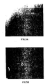
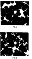
- the TEM pictures shown in Figs. 3A and 3B represent the disordered structure of a ten second silicon deposit of 600°C and 650°C respectively.
- the silicon structure is featureless and essentially amorphous. Even the 700°C and 800°C ten second silicon deposits show little crystalline structure in Figs. 3C and 3D respectively.
- Fig. 3E shows the TEM picture of a 900°C ten second silicon deposit which is still only partially crystallized.
- the pseudocrystalline silicon has high internal stress.
- the silicon atoms shift from their disordered positions into the ordered lattice sites around their respective nucleus. Since the interatomic distance of crystalline silicon is shorter than the pseudocrystalline silicon, the crystallization creates structural contraction. As a result, microcracks and microvoids can form in the silicon films. Shorts developed during subsequent processing (e.g. metallization) can be largely attributed to the presence of microcracks and microvoids.
- An isolation layer 4 of Si0 2 is then deposited over the polysilicon field shield 3 by the thermal decomposition (CVD) of silane in an oxidizing atmosphere such as the presence of oxygen in an inert carrier gas.
- This CVD oxide is indicated as CVD Oxide I.
- the thickness of this CVD oxide layer 4 can vary in accordance with processing requirements which illustratively may be in the range of about 200 to about 800 nm. The foregoing is a typical processing sequence for formation of a single level polysilicon device.
- a second layer 5 of polysilicon is deposited on the insulation oxide layer 4.
- This second polysilicon layer 5 is also indicated in the drawings as Poly II and will normally be doped, e.g. with phosphorous.
- a third layer 6 of silicon dioxide is deposited over the second polysilicon layer 5, by the pyrolytic deposition techniques.
- This third oxide layer 6 is also indicated as CVD Oxide II, and illustratively may be in a thickness range of about 400 to about 1200 nm.
- microcracks and microvoids in the polysilicon films or layer on developing interlayer shorts is illustrated in Figs. 2A to 2C. These microcracks or voids may not necessarily generate shorts. However, the presence of the microcracks and/or voids exposes the insulator oxide layer 4 under the microcracks and/or microvoids 7. During the doping of the Polysilicon II layer 5 (e.g. diffusion with POC1 3 ), the exposed oxide 10, under the p cracks and/or voids, converts into a phospho-silicate glass (PSG). In subsequent etching (e.g.
- the PSG or oxide 10 under the p-crack/p-void 7 is also etched, and hence, extending the ⁇ -crack/ ⁇ -void 7 into and through the insulator oxide layer 4 (CVD Oxide I) as a tunnel or gap 12.
- the extended micro cracks/p-voids 7/12 are filled with metal to form the short path extension 14 of the contact metallization 13.
- p-cracks/p-voids e.g. 7, in the polysilicon, e.g. layer 5 constitute a major factor in generating poly to poly shorts (e.g. from polysilicon layer 5 to polysilicon layer 3.
- the process of this invention for growing p-crack/p-void free polysilicon films and layers comprises, in its broad context, the formation, under controlled conditions and, on a compatible supporting substrate, a discrete amorphous silicon layer or film which is annealed to convert the amorphous silicon layer to its polycrystalline form 21A, followed by epitaxially extending the crystal grains, of the polycrystalline layer 21A, to the desired thickness 22, to form the desired novel polysilicon layer 23.
- the invention will be described with respect to the fabrication of CCD and random access memories, a fragmentary portion of which may be represented in Figs. 2A to 2C taken in conjunction with Fig. 1 and Figs. 4A to 4C for purposes of explanation.
- the invention will be described with reference to an intermediate structure fabricated up to the insulator oxide layer 4 with its sequential understructure of the field polysilicon layer 3, the thermally grown gate oxide 2 on a P-type silicon substrate 1.
- the gate oxide 2 may illustratively have a thickness of about 50 nm, with field polysilicon layer 3 having illustratively a thickness in the range of about 250 to about 400 nm.
- a thin continuous amorphous silicon film (see element 21, Fig. 4A) having a thickness less than about 100 nm, and preferably in the range of about 30 to about 50nm and optionally 50nm, is deposited by chemical vapor deposition on the insulator oxide layer 4, at a temperature of about 550° to about 600°C, and preferably from about 580° to about 600°C.
- the resultant-initial amorphous silicon structure, deposited at 600°C is shown in the Transmission -Electron Micrograph (TEM) of Fig. 3A.
- additional TEMs are shown for CVD deposited silicon (on Si0 2 , insulator oxide layer 4) at 650°C (Figs. 3B and 3F), at 700°C (Fig. 3C), at 800°C (Fig. 3D) and at 900°C (Fig 3E), in illustration of the difference in the deposited films at the various temperatures.
- the structure e.g. in Poly II layer 5 of Fig. 1, is put through an anneal cycle (normally in-situ in the deposition chamber) at a temperature of about 780°C to about 800°C, preferably at the upper 800°C limit, to transform the amorphous silicon into a fine equiaxial crystalline silicon (e.g. element 21A, Fig. 4B).
- the crystallized silicon grains usually have grain sizes equivalent to the amorphous film-thicknesses, i.e. about 50 nm grain size for 50 nm thick films and 30 nm grain size for 30 nm thick films.
- the heating time required for crystallization is about 20 to about 40 minutes.
- the equiaxial grain structure means that the grains are in their stable state, wherein further heating will cause little change in grain structure.
- the crystallized silicon layer will serve as a seed layer in subsequent deposition.
- microcracks/microvoids may form due to the fact that the interatomic distance of the crystal silicon is usually smaller than that of the amorphous silicon. However, these microcracks/voids will be filled during subsequent film growth.
- the temperature is reduced to about 680 to about 700°C, preferably 700°C, and the CVD deposition of silicon is resumed onto the fine grained polycrystalline seed layer 21A (Fig. 4B) to build up the film thickness 22 (Fig. 4C)), e.g. illustratively about 300 to about 600 nm, to form the novel polysilicon layer 23 (Fig. 4C) as required or desired for integrated circuit applications, e.g. the Poly II layer 5 of Fig. 1 and Figs. 2A to 2C.
- the deposition temperature must be sufficiently high to continue the substrate crystalline structure 21A, Fig. 4B, in an epi-like extension in the vertical direction but not enough to have lateral grain growth.
- the grain growth in the vertical direction is an epitaxial-like extension of the polycrystalline silicon seed layer grain structure, while in the lateral direction, it must interfere with the neighboring grain growth, thus requiring more energy.
- novel/modified polycrystalline films 23 (21A/22) grown in accordance with this invention as described above, will have fine grains and will be virtually free of p-cracks/p-voids.
- This fine grain structure is also desirable because the film asperity is small which results in reduced poly/ poly breakdown voltage degradation, e.g. between the Poly I layer 3 and the Poly II layer 5.
- the films are free of ⁇ - cracks/u-voids because the as-grown films have stable equiaxial grain structure which will resist structural changes even if the films are heated to 1000°C. It may be noted that the crystallization temperature of 800°C (for the amorphous silicon film 21, Fig. 4A) is much higher than the required minimum crystallization (anneal) temperature of about 650°C.
- the purpose here is to develop the film structure into stable equiaxial grains, where the crystallized grains are to later act as seed during subsequent silicon deposition.
- the temperature is lowered to 680°-700°C, which is again higher than the minimum polysilicon deposition temperature.
- Deposition at 680-700°c assures that the internal stress of the grown grains will be sufficiently low so that, in subsequent heatings, little grain growth will occur.
- this deposition temperature is sufficiently low so that the deposition will extend the seed structure in the vertical direction only with relatively little in the lateral direction, thus to limit the lateral grain growth during the deposition.
Abstract
Description
- This invention relates to the fabrication of semiconductor devices, and more particularly to a process for forming extended polycrystalline silicon structures in the fabrication of semiconductor devices such as integrated circuits.
- Polycrystalline silicon, or polysilicon as it is alternately referred to, is receiving much attention for many silicon devices. Typical applications of polysilicon can be found in the Anderson patent US 3 370 980 issued February 27, 1968; the Bean et al patent US 3 519 901 issued July 7, 1970; the Smith patent US 3 811 076 issued May 14, 1974; the Garnache patent US 3 841 926 issued October 15, 1974; the Lesk patent US 3 900 345 issued August 19, 1975; the Joshi et al patent US 4 123 300 issued October 31, 1978; the Wada et al article "Grain Growth Mechanism of Heavily Phosphorus-Implanted Polycrystalline Silicon", pp.1499-1504, J. Electrochem. Soc.: Solid State Technology, Vol.125, No.9, September 1978; the Sunami article "Thermal Oxidation of Phosphorus-Doped Polycrystalline Silicon in Wet Oxygen", pp.892-97, J. Electrochem. Soc.: Solid-State Science and Technology, Vol.125, No.6, June 1978; The Abbas article "FET Integrated Circuit Having Two Polysilicon Layers", pp.3022-23, IBM-TDB, Vol.15, No.lO, March 1973; the Fowler article "Reduction of Leakage in Si02 Grown on Silicon Films", p.1615, IBM-TDB, Vol.18, No.5, October 1975;-and the Irene article "Method to Avoid the Polysilicon Film Tearing Mechanism", p.4961, IBM-TDB, Vol.20, No.llB, April 1978.
- Polysilicon films have growing importance in the semiconductor fabrication art, particularly in the silicon gate technology which is employed in the fabrication of many MOS integrated circuits. In this technology, silicon dioxide films have been grown as intermediate insulators for double or higher level polysilicon devices for CCDs and random access memories. For another related application see the V.L. Rideout article "Double Polysilicon Dynamic Memory Cell With Polysilicon Bit Line", pp.3828-31, IBM-TDB, Vol.21, No.9, February 1979. However, this technology has encountered inter-polysilicon layer shorts (in the double polysilicon process) which constitutes one of the major yield detractors in the resultant semiconductor devices. Until recently it has been believed that the quality of silicon oxides grown on the polysilicon gates governed the reliability of these devices.
- Object of the invention is to provide a novel process for forming an improved layer of polysilicon on a substrate.
- The object of the invention is achieved by a process which is characterized in that a discrete
amorphous silicon layer 21A is formed onsubstrate 20, that the resultant structure is annealed to convertamorphous silicon layer 21A to a polycrystalline silicon layer, and that the crystal grains ofpolycrystalline silicon layer 21A are epitaxially extended to a desiredthickness 22. - With this process polysilicon layers of improved reliability in the fabrication of integrated circuit structures can be formed.
- In the accompanying drawings forming a material part of this disclosure:
- Fig. 1 is a schematic fragmentary sectional view illustrating a layered portion of a desired construction of a device fabricated by the double and/or higher level polysilicon technology.
- Figs. 2A to 2C are schematic fragmentary sectional views illustrating the development of interpoly shorts resulting from microvoids (p voids) and/or microcracks (p cracks) defects in deposited polysilicon structures.
- Figs. 3A to 3F are Transmission Electron Micrographs (TEM) of non-monocrystalline silicon layers deposited at various temperatures.
- Figs. 4A to 4C are schematic fragmentary sectional views illustrating the development of the novel polycrystalline layers of this invention.
- For further comprehension of the invention, and of the objects and advantages thereof, reference will be had to the following description and accompanying drawings, and to the appended claims in which the various novel features of the invention are more particularly set forth.
- Fig. 1 shows a desired construction of a portion of layered structure formed for the double and higher level polysilicon technology.
- As shown the structure is comprised of a monocrystalline silicon substrate 1 which is normally oxidized to provide an overlying dielectric or
insulating layer 2 represented as a gate Si02 in the figure. It is to be understood that although the silicon substrate is shown, for purposes of illustration of the invention, to be substantially undoped and without regions or pockets of different conductivity determining impurity types and concentration, that normally in the practice of the invention the substrate can be expected to have such regions conventional in integrated circuit devices which is inclusive of active and passive devices as well as means for isolating the devices from each other. - Deposited on the
gate oxide 2, is a layer of polycrystalline silicon (indicated as a polysilicon field shield 3) which may optionally be doped or undoped, and designated in the drawing as Poly I. Heretofore, the conventional practice of depositing polysilicon layers was by decomposition of silane (with in-situ or post deposition doping to desired conductivities) to the required thickness (e.g. about 200 to 600 nm) at a temperature of 600 to 650°C, mostly at around 620°C. The silicon deposited on an oxide covered silicon substrate by decomposition of silane at temperatures of 580°C to 650°C, which is commonly used in silicon gate and double polysilicon processes for LSI/VLSI, has a pseudocrystalline structure. The pseudocrystalline structure means that the silicon atoms do not have the periodicity of normal silicon crystal lattice. The silicon atoms are disordered and their interatomic distances are larger than the normal silicon crystal lattice parameter. The TEM pictures shown in Figs. 3A and 3B represent the disordered structure of a ten second silicon deposit of 600°C and 650°C respectively. The silicon structure is featureless and essentially amorphous. Even the 700°C and 800°C ten second silicon deposits show little crystalline structure in Figs. 3C and 3D respectively. Fig. 3E shows the TEM picture of a 900°C ten second silicon deposit which is still only partially crystallized. The pseudocrystalline silicon has high internal stress. In subsequent hot processing such as diffusion, oxidation and/or annealing, the silicon atoms shift from their disordered positions into the ordered lattice sites around their respective nucleus. Since the interatomic distance of crystalline silicon is shorter than the pseudocrystalline silicon, the crystallization creates structural contraction. As a result, microcracks and microvoids can form in the silicon films. Shorts developed during subsequent processing (e.g. metallization) can be largely attributed to the presence of microcracks and microvoids. - An
isolation layer 4 of Si02 is then deposited over thepolysilicon field shield 3 by the thermal decomposition (CVD) of silane in an oxidizing atmosphere such as the presence of oxygen in an inert carrier gas. This CVD oxide is indicated as CVD Oxide I. The thickness of thisCVD oxide layer 4 can vary in accordance with processing requirements which illustratively may be in the range of about 200 to about 800 nm. The foregoing is a typical processing sequence for formation of a single level polysilicon device. - In the fabrication of double and higher level polysilicon devices, a
second layer 5 of polysilicon, illustratively of about 200 to about 600 nm, is deposited on theinsulation oxide layer 4. Thissecond polysilicon layer 5 is also indicated in the drawings as Poly II and will normally be doped, e.g. with phosphorous. - As shown in the drawings a
third layer 6 of silicon dioxide is deposited over thesecond polysilicon layer 5, by the pyrolytic deposition techniques. Thisthird oxide layer 6 is also indicated as CVD Oxide II, and illustratively may be in a thickness range of about 400 to about 1200 nm. - The presence of microcracks and microvoids in the polysilicon films or layer on developing interlayer shorts is illustrated in Figs. 2A to 2C. These microcracks or voids may not necessarily generate shorts. However, the presence of the microcracks and/or voids exposes the
insulator oxide layer 4 under the microcracks and/ormicrovoids 7. During the doping of the Polysilicon II layer 5 (e.g. diffusion with POC13), the exposedoxide 10, under the p cracks and/or voids, converts into a phospho-silicate glass (PSG). In subsequent etching (e.g. with buffered hydrofluoric acid, BHF), as for opening contact windows orvias 11, the PSG oroxide 10 under the p-crack/p-void 7 is also etched, and hence, extending the µ-crack/µ-void 7 into and through the insulator oxide layer 4 (CVD Oxide I) as a tunnel orgap 12. During metallization (e.g. forcontact 13 utilizing conventional photolithographic techniques with resist 14), the extended micro cracks/p-voids 7/12 are filled with metal to form theshort path extension 14 of thecontact metallization 13. - In the manner indicated above, p-cracks/p-voids e.g. 7, in the polysilicon,
e.g. layer 5 constitute a major factor in generating poly to poly shorts (e.g. frompolysilicon layer 5 topolysilicon layer 3. - In accordance with this invention it has been found that by proper control of the nucleation and growth of polysilicon films or layers, p-cracks/p-voids can be virtually eliminated. The process of this invention for growing p-crack/p-void free polysilicon films and layers comprises, in its broad context, the formation, under controlled conditions and, on a compatible supporting substrate, a discrete amorphous silicon layer or film which is annealed to convert the amorphous silicon layer to its
polycrystalline form 21A, followed by epitaxially extending the crystal grains, of thepolycrystalline layer 21A, to the desiredthickness 22, to form the desirednovel polysilicon layer 23. - More specifically, the invention will be described with respect to the fabrication of CCD and random access memories, a fragmentary portion of which may be represented in Figs. 2A to 2C taken in conjunction with Fig. 1 and Figs. 4A to 4C for purposes of explanation. Also the invention will be described with reference to an intermediate structure fabricated up to the
insulator oxide layer 4 with its sequential understructure of thefield polysilicon layer 3, the thermally growngate oxide 2 on a P-type silicon substrate 1. In this intermediate structure thegate oxide 2 may illustratively have a thickness of about 50 nm, withfield polysilicon layer 3 having illustratively a thickness in the range of about 250 to about 400 nm. - In the continuing processing in accordance with this invention a thin continuous amorphous silicon film (see element 21, Fig. 4A) having a thickness less than about 100 nm, and preferably in the range of about 30 to about 50nm and optionally 50nm, is deposited by chemical vapor deposition on the
insulator oxide layer 4, at a temperature of about 550° to about 600°C, and preferably from about 580° to about 600°C. The resultant-initial amorphous silicon structure, deposited at 600°C is shown in the Transmission -Electron Micrograph (TEM) of Fig. 3A. For purposes of comparison, additional TEMs are shown for CVD deposited silicon (on Si02, insulator oxide layer 4) at 650°C (Figs. 3B and 3F), at 700°C (Fig. 3C), at 800°C (Fig. 3D) and at 900°C (Fig 3E), in illustration of the difference in the deposited films at the various temperatures. - Next, the structure, e.g. in
Poly II layer 5 of Fig. 1, is put through an anneal cycle (normally in-situ in the deposition chamber) at a temperature of about 780°C to about 800°C, preferably at the upper 800°C limit, to transform the amorphous silicon into a fine equiaxial crystalline silicon (e.g. element 21A, Fig. 4B). The crystallized silicon grains usually have grain sizes equivalent to the amorphous film-thicknesses, i.e. about 50 nm grain size for 50 nm thick films and 30 nm grain size for 30 nm thick films. The heating time required for crystallization is about 20 to about 40 minutes. The equiaxial grain structure means that the grains are in their stable state, wherein further heating will cause little change in grain structure. The crystallized silicon layer will serve as a seed layer in subsequent deposition. - It may be noted that during crystallization of the initial amorphous silicon film, microcracks/microvoids may form due to the fact that the interatomic distance of the crystal silicon is usually smaller than that of the amorphous silicon. However, these microcracks/voids will be filled during subsequent film growth.
- In the next operation, the temperature is reduced to about 680 to about 700°C, preferably 700°C, and the CVD deposition of silicon is resumed onto the fine grained
polycrystalline seed layer 21A (Fig. 4B) to build up the film thickness 22 (Fig. 4C)), e.g. illustratively about 300 to about 600 nm, to form the novel polysilicon layer 23 (Fig. 4C) as required or desired for integrated circuit applications, e.g. thePoly II layer 5 of Fig. 1 and Figs. 2A to 2C. - The deposition temperature must be sufficiently high to continue the
substrate crystalline structure 21A, Fig. 4B, in an epi-like extension in the vertical direction but not enough to have lateral grain growth. - As indicated, the grain growth in the vertical direction is an epitaxial-like extension of the polycrystalline silicon seed layer grain structure, while in the lateral direction, it must interfere with the neighboring grain growth, thus requiring more energy.
- The novel/modified polycrystalline films 23 (21A/22) grown in accordance with this invention as described above, will have fine grains and will be virtually free of p-cracks/p-voids. This fine grain structure is also desirable because the film asperity is small which results in reduced poly/ poly breakdown voltage degradation, e.g. between the
Poly I layer 3 and thePoly II layer 5. The films are free of µ- cracks/u-voids because the as-grown films have stable equiaxial grain structure which will resist structural changes even if the films are heated to 1000°C. It may be noted that the crystallization temperature of 800°C (for the amorphous silicon film 21, Fig. 4A) is much higher than the required minimum crystallization (anneal) temperature of about 650°C. The purpose here is to develop the film structure into stable equiaxial grains, where the crystallized grains are to later act as seed during subsequent silicon deposition. - It is further noted that the second or final CVD silicon deposition (e.g. for the epi-
like extension 22, Fig. 4B), the temperature is lowered to 680°-700°C, which is again higher than the minimum polysilicon deposition temperature. Deposition at 680-700°c assures that the internal stress of the grown grains will be sufficiently low so that, in subsequent heatings, little grain growth will occur. On the other hand, this deposition temperature is sufficiently low so that the deposition will extend the seed structure in the vertical direction only with relatively little in the lateral direction, thus to limit the lateral grain growth during the deposition. - While the invention has been illustrated and described with respect to preferred embodiments of the invention, it is to be understood that the invention is not to be limited to the precise construction herein disclosed and the right is reserved to all changes and modifications coming within the scope of the invention as defined in the appended claims.
Claims (9)
Applications Claiming Priority (2)
| Application Number | Priority Date | Filing Date | Title |
|---|---|---|---|
| US203039 | 1980-11-03 | ||
| US06/203,039 US4358326A (en) | 1980-11-03 | 1980-11-03 | Epitaxially extended polycrystalline structures utilizing a predeposit of amorphous silicon with subsequent annealing |
Publications (3)
| Publication Number | Publication Date |
|---|---|
| EP0051249A2 true EP0051249A2 (en) | 1982-05-12 |
| EP0051249A3 EP0051249A3 (en) | 1985-04-24 |
| EP0051249B1 EP0051249B1 (en) | 1988-04-20 |
Family
ID=22752213
Family Applications (1)
| Application Number | Title | Priority Date | Filing Date |
|---|---|---|---|
| EP81108974A Expired EP0051249B1 (en) | 1980-11-03 | 1981-10-27 | Process for forming epitaxially extended polycrystalline structures |
Country Status (4)
| Country | Link |
|---|---|
| US (1) | US4358326A (en) |
| EP (1) | EP0051249B1 (en) |
| JP (1) | JPS5796518A (en) |
| DE (1) | DE3176714D1 (en) |
Cited By (5)
| Publication number | Priority date | Publication date | Assignee | Title |
|---|---|---|---|---|
| FR2536210A1 (en) * | 1982-11-12 | 1984-05-18 | Rca Corp | POLYCRYSTALLINE SILICON LAYERS FOR SEMICONDUCTOR DEVICES AND METHOD FOR FORMING SEMICONDUCTOR DEVICE |
| EP0159252A2 (en) * | 1984-03-28 | 1985-10-23 | Fujitsu Limited | Process for the production of semiconductor devices by using silicon-on-isolation techniques |
| EP0221767A2 (en) * | 1985-10-30 | 1987-05-13 | Astrosystems, Inc. | Fault tolerant thin-film photovoltaic cell |
| EP0521644A1 (en) * | 1991-06-21 | 1993-01-07 | Nec Corporation | Method of manufacturing polysilicon film |
| GB2322733A (en) * | 1997-02-27 | 1998-09-02 | Nec Corp | Polysilicon electrodes for DRAM cells |
Families Citing this family (40)
| Publication number | Priority date | Publication date | Assignee | Title |
|---|---|---|---|---|
| GB2081018B (en) * | 1980-07-31 | 1985-06-26 | Suwa Seikosha Kk | Active matrix assembly for display device |
| US4483726A (en) * | 1981-06-30 | 1984-11-20 | International Business Machines Corporation | Double self-aligned fabrication process for making a bipolar transistor structure having a small polysilicon-to-extrinsic base contact area |
| JPS58194799A (en) * | 1982-05-07 | 1983-11-12 | Hitachi Ltd | Preparation of silicon single crystal |
| GB2131407B (en) * | 1982-11-12 | 1987-02-04 | Rca Corp | Method of formation of silicon dioxide layer |
| US4592799A (en) * | 1983-05-09 | 1986-06-03 | Sony Corporation | Method of recrystallizing a polycrystalline, amorphous or small grain material |
| US4588447A (en) * | 1984-06-25 | 1986-05-13 | Rockwell International Corporation | Method of eliminating p-type electrical activity and increasing channel mobility of Si-implanted and recrystallized SOS films |
| CA1239706A (en) * | 1984-11-26 | 1988-07-26 | Hisao Hayashi | Method of forming a thin semiconductor film |
| US4597160A (en) * | 1985-08-09 | 1986-07-01 | Rca Corporation | Method of fabricating a polysilicon transistor with a high carrier mobility |
| JPS6310573A (en) * | 1986-07-02 | 1988-01-18 | Oki Electric Ind Co Ltd | Manufacture of semiconductor device |
| US4912540A (en) * | 1986-12-17 | 1990-03-27 | Advanced Micro Devices, Inc. | Reduced area butting contact structure |
| US4760036A (en) * | 1987-06-15 | 1988-07-26 | Delco Electronics Corporation | Process for growing silicon-on-insulator wafers using lateral epitaxial growth with seed window oxidation |
| JPS6448411A (en) * | 1987-08-18 | 1989-02-22 | Fujitsu Ltd | Forming method of polysilicon layer |
| JPH0644633B2 (en) * | 1987-11-14 | 1994-06-08 | 山形日本電気株式会社 | Floating gate nonvolatile memory manufacturing method |
| US4897150A (en) * | 1988-06-29 | 1990-01-30 | Lasa Industries, Inc. | Method of direct write desposition of a conductor on a semiconductor |
| US5180690A (en) * | 1988-12-14 | 1993-01-19 | Energy Conversion Devices, Inc. | Method of forming a layer of doped crystalline semiconductor alloy material |
| NL9000324A (en) * | 1990-02-12 | 1991-09-02 | Philips Nv | METHOD FOR MANUFACTURING A SEMICONDUCTOR DEVICE |
| US5147826A (en) * | 1990-08-06 | 1992-09-15 | The Pennsylvania Research Corporation | Low temperature crystallization and pattering of amorphous silicon films |
| US5169806A (en) * | 1990-09-26 | 1992-12-08 | Xerox Corporation | Method of making amorphous deposited polycrystalline silicon thermal ink jet transducers |
| US5365875A (en) * | 1991-03-25 | 1994-11-22 | Fuji Xerox Co., Ltd. | Semiconductor element manufacturing method |
| US5192708A (en) * | 1991-04-29 | 1993-03-09 | International Business Machines Corporation | Sub-layer contact technique using in situ doped amorphous silicon and solid phase recrystallization |
| JP2855919B2 (en) * | 1991-10-24 | 1999-02-10 | 日本電気株式会社 | Semiconductor device and manufacturing method thereof |
| JP3197036B2 (en) * | 1991-11-14 | 2001-08-13 | 鐘淵化学工業株式会社 | Method for forming crystalline silicon thin film |
| JPH05234900A (en) * | 1992-02-19 | 1993-09-10 | Nec Corp | Manufacture of semiconductor device |
| KR950010859B1 (en) * | 1992-09-29 | 1995-09-25 | 현대전자산업주식회사 | Chamel polysilicon manufacturing method of thin-film transistor |
| US5444302A (en) * | 1992-12-25 | 1995-08-22 | Hitachi, Ltd. | Semiconductor device including multi-layer conductive thin film of polycrystalline material |
| US5326722A (en) * | 1993-01-15 | 1994-07-05 | United Microelectronics Corporation | Polysilicon contact |
| US20020053734A1 (en) | 1993-11-16 | 2002-05-09 | Formfactor, Inc. | Probe card assembly and kit, and methods of making same |
| JP3124473B2 (en) * | 1994-08-19 | 2001-01-15 | セイコーインスツルメンツ株式会社 | Semiconductor device and manufacturing method thereof |
| US5893949A (en) * | 1995-12-26 | 1999-04-13 | Xerox Corporation | Solid phase epitaxial crystallization of amorphous silicon films on insulating substrates |
| US8033838B2 (en) | 1996-02-21 | 2011-10-11 | Formfactor, Inc. | Microelectronic contact structure |
| US5843811A (en) * | 1996-04-10 | 1998-12-01 | University Of Florida | Method of fabricating a crystalline thin film on an amorphous substrate |
| US5773329A (en) * | 1996-07-24 | 1998-06-30 | International Business Machines Corporation | Polysilicon grown by pulsed rapid thermal annealing |
| US5879975A (en) * | 1997-09-05 | 1999-03-09 | Advanced Micro Devices, Inc. | Heat treating nitrogen implanted gate electrode layer for improved gate electrode etch profile |
| JP2000111952A (en) * | 1998-10-07 | 2000-04-21 | Sony Corp | Electrooptical device, driving substrate for electrooptical device and their preparation |
| US6281559B1 (en) * | 1999-03-03 | 2001-08-28 | Advanced Micro Devices, Inc. | Gate stack structure for variable threshold voltage |
| US6455903B1 (en) | 2000-01-26 | 2002-09-24 | Advanced Micro Devices, Inc. | Dual threshold voltage MOSFET by local confinement of channel depletion layer using inert ion implantation |
| JP4655495B2 (en) * | 2004-03-31 | 2011-03-23 | 東京エレクトロン株式会社 | Deposition method |
| KR100773123B1 (en) * | 2005-11-28 | 2007-11-02 | 주식회사 에이이티 | method for forming silicon film by two step deposition |
| CN103236400B (en) * | 2013-03-29 | 2015-07-08 | 京东方科技集团股份有限公司 | Production method of low-temperature polysilicon thin film and production method of thin-film transistor |
| KR20160029236A (en) * | 2014-09-04 | 2016-03-15 | 삼성전자주식회사 | Semiconductor device and manufacturing method of the same |
Citations (4)
| Publication number | Priority date | Publication date | Assignee | Title |
|---|---|---|---|---|
| US3900345A (en) * | 1973-08-02 | 1975-08-19 | Motorola Inc | Thin low temperature epi regions by conversion of an amorphous layer |
| US4134125A (en) * | 1977-07-20 | 1979-01-09 | Bell Telephone Laboratories, Incorporated | Passivation of metallized semiconductor substrates |
| US4226898A (en) * | 1978-03-16 | 1980-10-07 | Energy Conversion Devices, Inc. | Amorphous semiconductors equivalent to crystalline semiconductors produced by a glow discharge process |
| GB2056174A (en) * | 1979-08-10 | 1981-03-11 | Siemens Ag | Process for reducing the density of fast surface states inmos-components |
Family Cites Families (15)
| Publication number | Priority date | Publication date | Assignee | Title |
|---|---|---|---|---|
| US3370980A (en) * | 1963-08-19 | 1968-02-27 | Litton Systems Inc | Method for orienting single crystal films on polycrystalline substrates |
| US3479237A (en) * | 1966-04-08 | 1969-11-18 | Bell Telephone Labor Inc | Etch masks on semiconductor surfaces |
| US3533857A (en) * | 1967-11-29 | 1970-10-13 | Hughes Aircraft Co | Method of restoring crystals damaged by irradiation |
| US3558374A (en) * | 1968-01-15 | 1971-01-26 | Ibm | Polycrystalline film having controlled grain size and method of making same |
| US3519901A (en) * | 1968-01-29 | 1970-07-07 | Texas Instruments Inc | Bi-layer insulation structure including polycrystalline semiconductor material for integrated circuit isolation |
| GB1269359A (en) * | 1968-08-22 | 1972-04-06 | Atomic Energy Authority Uk | Improvements in or relating to semiconductors and methods of doping semiconductors |
| US3586542A (en) * | 1968-11-22 | 1971-06-22 | Bell Telephone Labor Inc | Semiconductor junction devices |
| JPS4837232B1 (en) * | 1968-12-04 | 1973-11-09 | ||
| US3730765A (en) * | 1970-09-15 | 1973-05-01 | Gen Electric | Method of providing polycrystalline silicon regions in monolithic integrated circuits |
| US4087571A (en) * | 1971-05-28 | 1978-05-02 | Fairchild Camera And Instrument Corporation | Controlled temperature polycrystalline silicon nucleation |
| US3811076A (en) * | 1973-01-02 | 1974-05-14 | Ibm | Field effect transistor integrated circuit and memory |
| US3841926A (en) * | 1973-01-02 | 1974-10-15 | Ibm | Integrated circuit fabrication process |
| US4123300A (en) * | 1977-05-02 | 1978-10-31 | International Business Machines Corporation | Integrated circuit process utilizing lift-off techniques |
| NL7810549A (en) * | 1978-10-23 | 1980-04-25 | Philips Nv | METHOD FOR MANUFACTURING A SEMICONDUCTOR DEVICE |
| US4249968A (en) * | 1978-12-29 | 1981-02-10 | International Business Machines Corporation | Method of manufacturing a metal-insulator-semiconductor utilizing a multiple stage deposition of polycrystalline layers |
-
1980
- 1980-11-03 US US06/203,039 patent/US4358326A/en not_active Expired - Lifetime
-
1981
- 1981-10-16 JP JP56164353A patent/JPS5796518A/en active Granted
- 1981-10-27 EP EP81108974A patent/EP0051249B1/en not_active Expired
- 1981-10-27 DE DE8181108974T patent/DE3176714D1/en not_active Expired
Patent Citations (4)
| Publication number | Priority date | Publication date | Assignee | Title |
|---|---|---|---|---|
| US3900345A (en) * | 1973-08-02 | 1975-08-19 | Motorola Inc | Thin low temperature epi regions by conversion of an amorphous layer |
| US4134125A (en) * | 1977-07-20 | 1979-01-09 | Bell Telephone Laboratories, Incorporated | Passivation of metallized semiconductor substrates |
| US4226898A (en) * | 1978-03-16 | 1980-10-07 | Energy Conversion Devices, Inc. | Amorphous semiconductors equivalent to crystalline semiconductors produced by a glow discharge process |
| GB2056174A (en) * | 1979-08-10 | 1981-03-11 | Siemens Ag | Process for reducing the density of fast surface states inmos-components |
Non-Patent Citations (2)
| Title |
|---|
| APPLIED PHYSICS LETTERS, vol. 36, no. 1, January 1980, pages 59-61, New York, uSA; J.C. BEAN et al.: "Evidence for void interconnection in evaporated amorphous silicon from epitaxial crystallization measurements" * |
| APPLIED PHYSICS LETTERS, vol. 37, no. 7, October 1980, pages 648-651, New York; USA; B.Y. TSAUR et al.: "Epitaxial alignment of polycrystalline Si films on (100) Si" * |
Cited By (9)
| Publication number | Priority date | Publication date | Assignee | Title |
|---|---|---|---|---|
| FR2536210A1 (en) * | 1982-11-12 | 1984-05-18 | Rca Corp | POLYCRYSTALLINE SILICON LAYERS FOR SEMICONDUCTOR DEVICES AND METHOD FOR FORMING SEMICONDUCTOR DEVICE |
| EP0159252A2 (en) * | 1984-03-28 | 1985-10-23 | Fujitsu Limited | Process for the production of semiconductor devices by using silicon-on-isolation techniques |
| EP0159252A3 (en) * | 1984-03-28 | 1988-09-28 | Fujitsu Limited | Process for the production of semiconductor devices by using silicon-on-isolation techniques |
| US5037774A (en) * | 1984-03-28 | 1991-08-06 | Fujitsu Limited | Process for the production of semiconductor devices utilizing multi-step deposition and recrystallization of amorphous silicon |
| EP0221767A2 (en) * | 1985-10-30 | 1987-05-13 | Astrosystems, Inc. | Fault tolerant thin-film photovoltaic cell |
| EP0221767A3 (en) * | 1985-10-30 | 1989-04-12 | Astrosystems, Inc. | Fault tolerant thin-film photovoltaic cell |
| EP0521644A1 (en) * | 1991-06-21 | 1993-01-07 | Nec Corporation | Method of manufacturing polysilicon film |
| GB2322733A (en) * | 1997-02-27 | 1998-09-02 | Nec Corp | Polysilicon electrodes for DRAM cells |
| US5885889A (en) * | 1997-02-27 | 1999-03-23 | Nec Corporation | Process of fabricating semiconductor device having doped polysilicon layer without segregation of dopant impurity |
Also Published As
| Publication number | Publication date |
|---|---|
| EP0051249B1 (en) | 1988-04-20 |
| JPS647488B2 (en) | 1989-02-09 |
| US4358326A (en) | 1982-11-09 |
| JPS5796518A (en) | 1982-06-15 |
| DE3176714D1 (en) | 1988-05-26 |
| EP0051249A3 (en) | 1985-04-24 |
Similar Documents
| Publication | Publication Date | Title |
|---|---|---|
| US4358326A (en) | Epitaxially extended polycrystalline structures utilizing a predeposit of amorphous silicon with subsequent annealing | |
| US4814292A (en) | Process of fabricating a semiconductor device involving densification and recrystallization of amorphous silicon | |
| US5464791A (en) | Method of fabricating a micro-trench storage capacitor | |
| US7176109B2 (en) | Method for forming raised structures by controlled selective epitaxial growth of facet using spacer | |
| JP2761685B2 (en) | Method for manufacturing semiconductor device | |
| US5411912A (en) | Method of making a semiconductor device comprising lower and upper silicon layers as capacitor electrodes | |
| KR19990072884A (en) | Method for producing a polycrystalline silicon structure | |
| EP0051500B1 (en) | Semiconductor devices | |
| JP2000208644A (en) | Sram cell and manufacture of the same | |
| JPH11150249A (en) | Forming method of uneven polysilicon layer and substrate treatment device used by the same and semiconductor memory device | |
| US6383851B2 (en) | Method to fabricate an intrinsic polycrystalline silicon film thin film transistor | |
| US10886130B2 (en) | Methods of forming crystalline semiconductor material, and methods of forming transistors | |
| KR19990006510A (en) | Integrated circuit manufacturing method | |
| JPH10335607A (en) | Manufacture of semiconductor device | |
| KR100574587B1 (en) | Contact between a monocrystalline silicon region and a polycrystalline silicon structure and method for producing such a contact | |
| JP2861343B2 (en) | Semiconductor device and manufacturing method thereof | |
| US6069060A (en) | Method of manufacturing a semiconductor device having a single crystal silicon electrode | |
| JPH09139360A (en) | Metal wiring formation of semiconductor element | |
| EP0428732B1 (en) | Method of producing semiconductor devices | |
| JP2872425B2 (en) | Method for forming semiconductor device | |
| JPH05211288A (en) | Semiconductor device | |
| KR19980055759A (en) | Polysilicon Layer Formation Method | |
| JPH05299348A (en) | Forming method for polysrystalline silicon thin film | |
| RU2170474C2 (en) | Method for producing resistors in integrated circuits | |
| JPH02174237A (en) | Manufacture of semiconductor device |
Legal Events
| Date | Code | Title | Description |
|---|---|---|---|
| PUAI | Public reference made under article 153(3) epc to a published international application that has entered the european phase |
Free format text: ORIGINAL CODE: 0009012 |
|
| 17P | Request for examination filed |
Effective date: 19811027 |
|
| AK | Designated contracting states |
Designated state(s): DE FR GB |
|
| PUAL | Search report despatched |
Free format text: ORIGINAL CODE: 0009013 |
|
| AK | Designated contracting states |
Designated state(s): DE FR GB |
|
| 17Q | First examination report despatched |
Effective date: 19860821 |
|
| GRAA | (expected) grant |
Free format text: ORIGINAL CODE: 0009210 |
|
| AK | Designated contracting states |
Kind code of ref document: B1 Designated state(s): DE FR GB |
|
| REF | Corresponds to: |
Ref document number: 3176714 Country of ref document: DE Date of ref document: 19880526 |
|
| ET | Fr: translation filed | ||
| PLBE | No opposition filed within time limit |
Free format text: ORIGINAL CODE: 0009261 |
|
| STAA | Information on the status of an ep patent application or granted ep patent |
Free format text: STATUS: NO OPPOSITION FILED WITHIN TIME LIMIT |
|
| 26N | No opposition filed | ||
| PGFP | Annual fee paid to national office [announced via postgrant information from national office to epo] |
Ref country code: GB Payment date: 19910923 Year of fee payment: 11 |
|
| PGFP | Annual fee paid to national office [announced via postgrant information from national office to epo] |
Ref country code: FR Payment date: 19911001 Year of fee payment: 11 |
|
| PGFP | Annual fee paid to national office [announced via postgrant information from national office to epo] |
Ref country code: DE Payment date: 19911102 Year of fee payment: 11 |
|
| PG25 | Lapsed in a contracting state [announced via postgrant information from national office to epo] |
Ref country code: GB Effective date: 19921027 |
|
| GBPC | Gb: european patent ceased through non-payment of renewal fee |
Effective date: 19921027 |
|
| PG25 | Lapsed in a contracting state [announced via postgrant information from national office to epo] |
Ref country code: FR Effective date: 19930630 |
|
| PG25 | Lapsed in a contracting state [announced via postgrant information from national office to epo] |
Ref country code: DE Effective date: 19930701 |
|
| REG | Reference to a national code |
Ref country code: FR Ref legal event code: ST |