EP0048979A2 - Echo-Entzerrer für ein Fernsprechnetz mit langen Entfernungen - Google Patents
Echo-Entzerrer für ein Fernsprechnetz mit langen Entfernungen Download PDFInfo
- Publication number
- EP0048979A2 EP0048979A2 EP81107650A EP81107650A EP0048979A2 EP 0048979 A2 EP0048979 A2 EP 0048979A2 EP 81107650 A EP81107650 A EP 81107650A EP 81107650 A EP81107650 A EP 81107650A EP 0048979 A2 EP0048979 A2 EP 0048979A2
- Authority
- EP
- European Patent Office
- Prior art keywords
- echo
- digital signal
- digital
- signal
- incoming
- Prior art date
- Legal status (The legal status is an assumption and is not a legal conclusion. Google has not performed a legal analysis and makes no representation as to the accuracy of the status listed.)
- Granted
Links
- 238000005070 sampling Methods 0.000 claims abstract description 75
- 230000004044 response Effects 0.000 claims description 14
- 238000004891 communication Methods 0.000 claims description 5
- 238000010586 diagram Methods 0.000 description 12
- 238000002592 echocardiography Methods 0.000 description 7
- 238000000034 method Methods 0.000 description 6
- 230000005540 biological transmission Effects 0.000 description 5
- 230000008878 coupling Effects 0.000 description 3
- 238000010168 coupling process Methods 0.000 description 3
- 238000005859 coupling reaction Methods 0.000 description 3
- 238000012545 processing Methods 0.000 description 3
- 238000012986 modification Methods 0.000 description 2
- 230000004048 modification Effects 0.000 description 2
- 238000013459 approach Methods 0.000 description 1
- 230000008054 signal transmission Effects 0.000 description 1
- 238000004088 simulation Methods 0.000 description 1
Images


Classifications
-
- H—ELECTRICITY
- H04—ELECTRIC COMMUNICATION TECHNIQUE
- H04B—TRANSMISSION
- H04B3/00—Line transmission systems
- H04B3/02—Details
- H04B3/20—Reducing echo effects or singing; Opening or closing transmitting path; Conditioning for transmission in one direction or the other
- H04B3/23—Reducing echo effects or singing; Opening or closing transmitting path; Conditioning for transmission in one direction or the other using a replica of transmitted signal in the time domain, e.g. echo cancellers
Definitions
- the present invention relates to an echo canceller for eliminating undesirable echo appearing in a long-distance telephone network and, more particularly, to an echo canceller suited for a long-distance digitized telephone network where the incoming and outgoing digital signals have mutually different sampling rates.
- the master clock sources disposed at both ends of the four-wire circuit are subjected to frequency fluctuation, with the result that the timings of the sampling pulses produced by the counting-down of the master clock pulses differ from each other.
- the proposed echo canceller in which no attention is paid to the above-mentioned frequency fluctuation, is not suited for the accurate echo cancellation between the talker's echo and an estimated echo.
- An object of the present invention is, therefore, to provide an echo canceller free from the disadvantages in the prior art.
- an echo canceller for use in a long-distance telephone network having a four-wire circuit and a two-wire circuit, and responsive to an incoming digital signal supplied from the reception-side path of said four-wire circuit and to an unprocessed digital signal including a digital echo signal supplied to the input of the transmission-side path with an outgoing digital signal substantially free from said digital echo signal, said digital echo signal being inevitably produced at the junction of the four-wire circuit and the two-wire circuit, said incoming and outgoing digital signals having mutually different sampling rates.
- the present echo canceller is characterized by comprising: a sample interpolator for converting said incoming digital signal into a digital signal having the same sampling rate as that of the outgoing digital signal on the basis of relative positions of the sampling timings for corresponding imaginary envelopes of the incoming and outgoing digital signals: an echo estimator responsive to the output of the sample interpolator for producing an estimated echo signal to cancel said echo signal; and means for subtracting the estimated echo signal from the unprocessed digital signal to produce an echo cancelled digital signal.
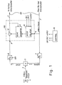
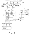
- a long-distance telephone network to which the present invention is applicable has a local two-wire circuit 3 connected to a subscriber set 4, a long-distance four-wire circuit 120 made of a submarine cable or a communication satellite link, and a hybrid circuit 5 for coupling these two-wire and four-wire circuits 3 and 120 to each other.
- D/A digital-to-analog
- A/D' analog-to-digital converter 8 for digitizing an analog speech signal supplied from the subscriber set 4.
- the output of the A/D converter 8 is transmitted to the long-distance four-wire circuit 120 through an echo canceller 100 of the present invention to which the outgoing digital signal and the incoming digital signal are supplied through terminals 9 and 6, respectively.
- a timing pulse generator 16 is also provided for providing sampling pulses CK1 and CK2 to the A/D converter 8 and the echo canceller100
- the echo canceller 100 has a sample interpolator 10 for converting the sampling rate of the incoming digital signal into another sampling rate preset for the signal digitization at the A/ D converter 8 for transmission. For this purpose, the so-called interpolation process is employed.
- the output of the sample interpolator is supplied to an echo estimator 11 for producing an estimated echo signal, i.e., a replica of the incoming signal, which causes the talker's echo when transmitted back to the other end of the four-wire circuit 120.
- a subtractor 12 is also provided for subtracting the estimated echo signal from the outgoing digital signal. For details of the subtractor 12 and the echo estimator 11, reference is made to Fig. 1 of the U.S. Patent No. 4,064,379.
- the output of the A/D converter 113, the subtractor 114, the output of the A/D converter 105, and the output of the register 111 shown in Fig. 1 of the above-mentioned U.S. Patent correspond to the terminal 9, the subtractor 12, the input of the estimator, and the output of the estimator 11 of the present invention, respectively.
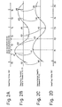
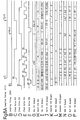
- time-sequential codewords which constitute the incoming digital signal supplied to the echo canceller 100 and respectively represent the signal samples digitized at the other end of the four-wire circuit 120 in response to a sampling pulse CK2 (Fig. 2A) are shown as imaginary decoded samples X0, X1, X2, .... X6, .... with an imaginary envelope.
- the samples X0, X1, X2, ...., X6 .... correspond to the sampling timings t0, tl, t2, .... t6 .... which are defined by a clock pulse source disposed at the other end of the long-distance four-wire circuit.
- the telephone signal supplied from the subscriber set 4 for transmission from this end of the four-wire circuit 120 is digitized at the A/D converter 8 in response to another sampling pulse CK1 (Fig. 2D) which has timings T0, T1, T2, .... T6, ....
- the leaked portion of the incoming signal applied to the A/D converter 8 is also sampled by the sampling pulse CK1 together with the outgoing telephone signal.
- the estimated echo signal must be in timed relationship with the outgoing digital signal.
- the estimated echo signal does not necessarily reflect a faithful simulation of the leaked portion of the incoming signal, making the echo cancellation difficult.
- the present invention relies on the so-called sample interpolation process, in which the sample codewords X0, X1, X2, .... and X6 .... are translated to approximated sample codewords Y0, YI, Y2, .... Y6 .... timed with the sampling pulse CK1.
- sample interpolation The simplest process to achieve such sample interpolation is to obtain the sample codewords Y0 to Y5 at the timings TO to T5 by the use of the sample codewords XO to X5.
- the sample codeword Y1 for example, positioned between the timings tl and t2 can be obtained using the sample codewords X1 and X2.
- the sample codeword Y2 can be obtained using the sample codewords X2 and X3.
- Such sample interpolation is achieved with a digital filter having a group of filter coefficients.
- sample interpolator used in the present invention can achieve more accurate sample interpolation in the following manner:
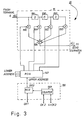
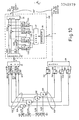
- the sample interpolator 10 shown in Fig. 1 comprises a transversal filter 15 having an input terminal for receiving the incoming digital signal through the terminal 6 and an output terminal connected to the estimator 11, a read-only memory (ROM) 140 for storing the four coefficient groups of the filter 15, and an address generator 130 for generating an address for accessing the ROM 140.
- the filter 15 consists of three delay elements 1515 to 1517, four multipliers 1510 to 1513, and an adder 1514 for adding up the outputs of the multipliers 1510 to 1513.
- the generator 130 is made up of a counter 1301 and a register 1302.
- the counter 1301 cleared by the sampling pulse CK2 performs the counting-up operation by a timing pulse 4xCK2 having the repetition cycle four times as fast as that of the sampling pulse CK2.
- the register 1302 stores the output of the counter 130 in response to the sampling pulse CK1 to give an upper address for the ROM140.
- Lower addresses "00", “10", “01” and “11” are fixedly given to the ROM140 as constant values.
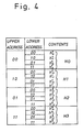
- Fig. 4 shows typical filter coefficient groups.
- a specific one of coefficient groups HO to H3 is designated by a corresponding one of upper addresses “0" to "3”, while coefficients, or contents of the coefficient group designated are given using the lower address "0" to "3".
- Fig. 5 shows a timed relationship between the sampling timings in synchronism with the sampling pulses CK1 and CK2 and the outputs of the main structural elements of Fig. 3.
- the sampling timing Tj (Fig. 5A) in synchronism with the outgoing digital signal with the sampling pulse CK1 (Fig. 5c) lies in the segment IA of a sampling interval k (Fig. 5B) in synchronism with the incoming digital signal with the sampling pulse CK2 (Fig. 5D).
- the register 1302 shown in Fig. 3 stores the output "0" (Fig. 5F) of the counter 1301 in response to the sampling pulse CK1
- an upper address "0" is given to the ROM140 to produce the coefficient group HO (Fig. 4).
- the ROM140 gives the coefficient h o 0 to h 3 o (Fig. 5G) to the multipliers 1510 to 1513.
- a sample codeword X(k) (Fig. 51) fed to the terminal 6 at the timing Tk (Fig. 5B) is applied to the multiplier 1510.
- sample codewords X(k-1), X(k-2), and X(k- 3) which were supplied to the terminal 6 at sampling timings T(k-1), T(k-2), and T(k-3) preceding the present timing Tk, are given to the multipliers 1511 to 1513 through the delay elements 1515 to 1517, respectively.
- the coefficients h 0 0 to h 3 0 are multiplied by the sample codewords X(k) to X(k-3) in the multipliers 1510 to 1513, respectively, and then added at the adder 1514 (See Fig. 3), to provide the sample codeword Y(j) (Fig. 5H) to be interpolated.
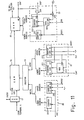
- FIG. 6 another example of the interpolator 10 shown in Fig. 1 is composed of a digital filter 15 having a multiplier 151 and an accumulator 152, a coefficient circuit 14 made up of a read-only memory (ROM) for storing the coefficients of the filter 15, a circuit 12 for supplying sample codewords to the digital filter 15, an address generator 13 for producing address for accessing the coefficient circuit 14, and a timing pulse generator 16 for generating pulses to control these circuits 12, 13, and 15.
- ROM read-only memory
- the circuit 12 further comprises a register 121 for storing input sample codewords in response to the sampling pulse CK2, a selector 122 for receiving the output of the register 121 at an input terminal B and the output of a shift register 123 at an input terminal A to select either the register 121 or the shift register 123 with a timing pulse CK5, and the four-stage shift register 123 for sequentially shifting the output of the selector 122 in response to timing pulses CK3 and CK4.
- the address generator 13 includes counters 131 and 133, and a register 132. The counter 131 and the register 133 perform the same operations as those in the counter 1301 and register 1302 shown in Fig. 3, respectively. After a predetermined value is set in the counter 133 by the sampling pulse CK1, the counting-down operation of the counter 133 is done starting from that value in response to the timing pulse CK3.
- a part 160 of the timing pulse generator 16 consists of a four-stage shiftregister 161, an OR gate 162, a delayed-type flip-flop 163, an AND gate 164, and a monostable multivibrator 165 so as to generate the timing pulses CK3 and CK4.
- the shift register 161 has a clear terminal CL for receiving a leading edge of the sampling pulse CK1 and an input terminal for receiving 1".
- the OR gate 162 produces a logical sum of the output of the register 161 and the input flip-flop sampling pulse CK1 is set in the lb3 with the sampling pulse CK2.
- the AND gate 164 produces a logical product of the output of the flip-flop 163 and that of the register 161.
- the multivibrator 165 inverts the output of the gate 164.
- Figs. 8A to 8P show diagrams for describing the operation of the sample interpolator shown in Fig. 6. This operation will be described in detail hereunder referring to Figs. 6 to 8 under the state where the positional relationship between the sampling timings Tj (Fig. 8A) and Tk (Fig. 8B) is the same as that in Fig.. 5.
- the sample codeword X(k) (Fig. 8G) fed to the terminal 6 is stored in the register 122 at the leading edge El of the sampling pulse CK2 (Fig. 8D).
- the register 123 are stored sample codewords X(k-4), X(k-3), X(k-2), and X(k-1), which were respectively given to the terminal 6 at sampling timings T(k-4), T(k-3), T(k-2), and T(k-I) preceding the present timing Tk.
- an initial value "0" (Fig. 8K) is set in the counter 131.
- the selector 122 is then switched at the trailing edge E2 (Fig.
- the selector 122 selects the terminal A in response to a selection signal CK5 (Fig. 8H) from the circuit 16. Since the counter 133 gives a lower address "2" to the coefficient circuit 14 at the leading edge E6 of the timing pulse CK3, the coefficient circuit 14 feeds the coefficient h 2 0 to the multiplier 151. Further, at this leading edge E6, the register 123 gives the sample codeword X(k-2) to the multiplier 151, so that the sample codeword X(k-2) multiplied by the coefficient h 2 0 at the multiplier 151 is fed to the accumulator 152 as the product Yl.
- the accumulator 152 then accumulates the products YO and Y1 obtained at the leading edge E6.
- the same procedure as at the leading edge E6 is performed for the sample codewords X(k-1) and X(k) at the leading edges E7 and E8.
- the accumulator 152 calculates the total sum of the products obtained at the leading edges E4 and E6-E8, i.e., the interpolation sample codeword Y(j).
- the sample codeword to be interpolated at the sampling timing Tj is obtained in this manner.
- each waveform is produced upon coincidence of the sampling timing Tj (Fig. 9A) with the sampling timing Tk (Fig. 9B).
- the multiplication by the filter 15 is started after the leading edge of the timing pulse CK1 (Fig. 8C)
- no input sample codeword after the leading edge of the sampling pulse CK2 (Fig. 8D) can be stored in the shift register 123. Therefore, the storing of the input sample codeword in the register 123 takes place after the completion of the multiplication by the filter 15. Since other operations are the same as those illustrated in Fig. 8, further description will be omitted.
- another long-distance telephone network to which the present invention is applicable has local two-wire circuits 3-1 to 3-24 connected to subscriber sets 401-424, a four-wire circuit 120' made of 24-channel communication lines and hybrid circuits 501 to 524 for coupling the two-wire and four-wire circuits to each other, and a multiplexer 25 and a demultiplexer 24 for performing the multiplexing and demultiplexing to and from such communication lines 120'.
- D/A converters 701 to 724 To the reception sides of the circuits 501 to 524 are connected D/A converters 701 to 724 and to the transmission sides of the circuits 501 to 524 are connected to A/D converters 801 to 824.
- the outputs of the A/D converters 801 to 824 are given to the circuit 120' through an echo canceller 200 of the invention designed for the 24-channel time division multiplex communication.
- an echo canceller 200 of the invention designed for the 24-channel time division multiplex communication.
- the 24-channel multiplexed digital signal with the reception cycle 24 times as fast as that of the timing pulse CK2 is supplied through the digital reception side path 1 to both the reception terminal 6 of an echo canceller 200 and a demultiplexer 24.
- the demultiplexer 24 separates the multiplexed digital signal into the incoming digital signals corresponding to each of 24 channels.
- the demultiplexed signals are converted into original telephone signals by D/A converters 701 to 724 provided in one-to-one correspondence to 24 channels and supplied through hybrid circuits 501 to 524 to subscriber sets 401 to 424. All the circuits 501 to 524 produce echoes and supply them to A/D converters 801 to 824.
- the digitized echoes converted by the converters 801 to 824 are multiplexed by a multiplexer 25 and fed to a demultiplexer 26 through a transmission terminal 9 of the canceller 200.
- the multiplexed digital echo signal is separated by the demultiplexer 26 into the digital echo signals corresponding to each of 24 channels.
- the 24-channel multiplexed digital signal given to the terminal 6 is converted into a digital signal with the sampling pulse 24CK1 by an interpolator 20 to be described hereunder.
- the output of the interpolator 20 is separated by a demultiplexer 27 into outputs corresponding to 24 channels, so that the separated signals are supplied to echo estimators 1101 to 1124.
- the echo estimators 1101 to 1124 in response to the outputs fed by the demultiplexer 27, produce estimated echoes to be sent to subtractors 1201 to 1224.
- Each of the subtractors 1201 to 1224 performs the subtraction between each digital echo signal from the demultiplexer 26 and each of the estimated echoes.
- the outputs of the subtractors 1201 to 1224 (residual echoes) are again supplied to the estimators 1101 to 1124 to bring the estimated echoes closer to the true echoes.
- Fig. 11 shows a part of the interpolator 20 shown in Fig. 10.
- the 24-channel structure of the interpolator 20 corresponding to the single-channel structure (consisting of the register 121 and the selector 122) shown in Fig. 6 includes a register 17, a random access memory (RAM) 18, a read address generator 21, a write address generator 20, and a selector 19 for switching between these circuits 20 and 21.
- the RAM 18 has 24 storage areas, each corresponding to each channel to store three sample codewords X(k-1), X(k-2), and X(k-3), which have been respectively given to the terminal 6 at sampling timings T(k-1), T(k-2), and T(k-3) preceding the present sampling timing Tk.
- the write address generator 20 comprises counters 201 and 302.
- the counting-up operation of the counter 202 is performed by the sampling pulse 24CK2 24 times as fast as the sampling pulse CK2, while the counter 201 is counted up in synchronism with the sampling pulse CK2.
- the counter 202 generates an upper address for designating achannel number, whereas the counter 201 generates a lower address for designating one of sample codewords stored in the memory area corresponding to the channel 1.
- the read adddress generator 21 is made up of counters 211 and 213, and a register 212. "1" is set in the counter 213 as the initial value corresponding to the channel 1 by the sampling pulse CK1.
- the counting" up operation of the counter 213 is performed in response to the sampling pulse 24CK1 24 times as fast as the sampling pulse CK1, while the counter 211 is counted up by the timing pulse CK4'.
- the register 212 stores the output of the counter 211 in synchronism with the sampling pulse CK1.
- the counter 213 generates an upper address for designating a channel number, whereas the counter 211 generates a lower address for designating one of sample codewords stored in the memory area corresponding to the channel number designated by the counter 213.
- the 24-channel structure corresponding to the single channel (consisting of the shift resister 123) shown in Fig. 6 is composed of an RAM 22 and an address generator 23 of the RAM 22 ,
- the RAM 22 has 24 storage areas, each of which corresponds to each channel, to store four sample codewords required for obtaining one interpolation value for each channel.
- the address generator 23 is composed of counters 221 and 222, an adder 225, and a register 223.
- the counter 221 is counted up by the clock 24CK1, while counter 222 is counted up by the output of an AND gate 224.
- the adder 225 adds "1" to the output of the counter 222.
- the register 223 stores the output of the adder 225 in synchronism with the sampling pulse CK1.
- the counter 221 generates an upper address for designating a channel number, whereas the counter 222 generates a lower address for designating one of sample codewords stored in the memory area corresponding to the channel number.
- the timing pulses CK3' and CK4' respectively correspond to the timing pulses CK3 and CK4 shown in Fig. 6 .
- Figs. 12A to 12L show diagrams for describing the operation of the sample interpolator shown in Fig. 11. This operation will be described indetail hereunder referring to Figs. 6 and 10 assuming the state where the positional relationship between the sampling timings Tj (Fig. 12A) and Tk (Fig. 12B) is the same as that in Fig. 9.
- FIG. 12E A 24-channel time division multiplexed digital signal (Fig. 12E) is supplied to the terminal 6 in each period equal to one twenty-fourth of one sampling period.
- timing pulse 1 (Fig. 12 F)
- the sample codeword X(k) on the channel 1 (Fig. 12E, 12G) fed to the terminal 4 is stored in the register 17 in synchronism with the sampling pulse 24CK2 (Fig. 121).
- the write address generator 20 gives an address designating the channel 1 to the RAM 18 via the selector 19, the output X(k) (Fig. 12J) of the register 17 is stored in the memory area corresponding to the channel 1 of the RAM 18.
- the counters 221 and 222 give the RAM 35 an address "1" for designating the channel 1 and an address "0" for designating the 0-th sample on the channel 1, respectively, so that the RAM 22 gives the sample codeword X(k-7) (Fig. 12L) to the multiplier 151 (Fig. 6).
- the coefficient circuit 14 (Fig. 6), in response to the address from the address generator 13 (Fig. 6), supplies the multiplier 151 with a coefficient h 3 3 corresponding to the 0-th sample codeword on the channel 1.
- the sample codeword X(k-7) multiplied by the coefficient h 3 3 at the multiplier 151 is given to the accumulator 152.
- the sample codewords X(k-6), X(k-5), and X(k-4) stored in the memory area corresponding to the channel 1 in the RAM 22 are read and supplied to the multiplier 151.
- Each of the sample codewords X(k-6), X(k-5), and X(k-4) multiplied by the corresponding coefficients h 2 3 , h 1 3 , and h 0 3 , respectively, is fed to the accumulator 152.
- the sample value to be interpolated on the channel 1 is determined in this manner.
- the oldest sample codewords X(k-7) and X(k-6) on the channel 1 are replaced with the next sample codewords X(k-3) and X(k-2) (Fig. 12K) so as to obtain a value to be interpolated.at the next sampling timing for the channel 1.
- the same procedure is applied to the channels 2 to 24.
- the sample interpolators 10 and 20 are connected to the terminal 6 in the foregoing embodiments, they may be connected to the terminal 9.
Landscapes
- Engineering & Computer Science (AREA)
- Computer Networks & Wireless Communication (AREA)
- Signal Processing (AREA)
- Cable Transmission Systems, Equalization Of Radio And Reduction Of Echo (AREA)
- Synchronisation In Digital Transmission Systems (AREA)
Applications Claiming Priority (2)
| Application Number | Priority Date | Filing Date | Title |
|---|---|---|---|
| JP55134009A JPS6046899B2 (ja) | 1980-09-26 | 1980-09-26 | 反響消去装置 |
| JP134009/80 | 1980-09-26 |
Publications (4)
| Publication Number | Publication Date |
|---|---|
| EP0048979A2 true EP0048979A2 (de) | 1982-04-07 |
| EP0048979A3 EP0048979A3 (en) | 1983-06-29 |
| EP0048979B1 EP0048979B1 (de) | 1986-04-23 |
| EP0048979B2 EP0048979B2 (de) | 1990-08-08 |
Family
ID=15118239
Family Applications (1)
| Application Number | Title | Priority Date | Filing Date |
|---|---|---|---|
| EP81107650A Expired EP0048979B2 (de) | 1980-09-26 | 1981-09-25 | Echo-Entzerrer für ein Fernsprechnetz mit langen Entfernungen |
Country Status (5)
| Country | Link |
|---|---|
| US (1) | US4527020A (de) |
| EP (1) | EP0048979B2 (de) |
| JP (1) | JPS6046899B2 (de) |
| CA (1) | CA1178731A (de) |
| DE (1) | DE3174473D1 (de) |
Cited By (4)
| Publication number | Priority date | Publication date | Assignee | Title |
|---|---|---|---|---|
| EP0074089A1 (de) * | 1981-09-09 | 1983-03-16 | Communications Satellite Corporation | Digitaler Bitraten-Synchronisierer für digitale Echoentzerrer und ähnliche signalverarbeitende Einrichtungen |
| US4481385A (en) * | 1981-05-07 | 1984-11-06 | U.S. Philips Corporation | Arrangement for cancelling echo signals |
| EP0122594A3 (de) * | 1983-04-18 | 1986-09-10 | International Standard Electric Corporation | Leitungsschaltung mit Echokompensation |
| EP0334587A3 (de) * | 1988-03-22 | 1991-12-04 | Fujitsu Limited | Signalverarbeitungssystem |
Families Citing this family (22)
| Publication number | Priority date | Publication date | Assignee | Title |
|---|---|---|---|---|
| EP0137323B1 (de) * | 1983-10-06 | 1989-03-29 | Studer Revox Ag | Verfahren und Vorrichtung zur Umsetzung einer Eingangsabtastfolge in eine Ausgangsabtastfolge |
| DE3586696T2 (de) * | 1984-05-30 | 1993-04-01 | Hitachi Ltd | Pcm-coder/decoder mit zweidraht/vierdrahtumwandlung. |
| NZ214905A (en) * | 1985-01-29 | 1988-09-29 | British Telecomm | Noise cancellation by adaptive filter compensates for timing variations |
| DE3576772D1 (de) * | 1985-04-30 | 1990-04-26 | Ibm | Verfahren und vorrichtung zur echoannullierung in einem uebertragungsnetzwerk. |
| JPH0720070B2 (ja) * | 1985-08-14 | 1995-03-06 | 株式会社日立製作所 | デイジタル平衡回路を有するpcm符号復号器 |
| NL8600815A (nl) * | 1986-03-28 | 1987-10-16 | At & T & Philips Telecomm | Inrichting voor het kompenseren van niet-lineaire vervorming in een te digitaliseren ingangssignaal en een echokompensatiestelsel voorzien van een dergelijke inrichting. |
| NO180137C (no) * | 1986-11-17 | 1997-02-19 | Alcatel Nv | Ekkokansellerings-anlegg |
| FR2614484B1 (fr) * | 1986-12-30 | 1994-04-08 | Telecommunications Sa | Terminal de transmission de donnees sur une voie analogique bidirectionnelle avec annulation d'echo couplee au rythme reception |
| WO1989007370A1 (en) * | 1988-02-01 | 1989-08-10 | Concord Data Systems, Inc. | Far end echo cancellation method and apparatus |
| US4995030A (en) * | 1988-02-01 | 1991-02-19 | Memotec Datacom, Inc. | Far end echo cancellation method and apparatus |
| US4866647A (en) * | 1988-02-04 | 1989-09-12 | American Telephone And Telegraph Company | Continuously variable digital delay circuit |
| JP2520770B2 (ja) * | 1990-07-06 | 1996-07-31 | 富士通株式会社 | ハイブリッド回路 |
| JPH05122106A (ja) * | 1991-05-22 | 1993-05-18 | Hitachi Ltd | 半導体集積回路装置 |
| US5475628A (en) * | 1992-09-30 | 1995-12-12 | Analog Devices, Inc. | Asynchronous digital sample rate converter |
| US5638010A (en) * | 1995-06-07 | 1997-06-10 | Analog Devices, Inc. | Digitally controlled oscillator for a phase-locked loop providing a residue signal for use in continuously variable interpolation and decimation filters |
| KR100240626B1 (ko) * | 1997-11-25 | 2000-01-15 | 정선종 | 디지털 이동 통신 시스템에서의 반향 제거 방법 및 장치 |
| US20020021693A1 (en) * | 1998-05-01 | 2002-02-21 | At&T Corp. | Sharing of voice-switched network and internet resources for intelligent session processing |
| US6563802B2 (en) * | 1998-06-22 | 2003-05-13 | Intel Corporation | Echo cancellation with dynamic latency adjustment |
| US6647022B1 (en) * | 1998-08-07 | 2003-11-11 | Lucent Technologies Inc. | Interference canceller |
| US7839758B1 (en) * | 2008-09-23 | 2010-11-23 | Net Logic Microsystems, Inc. | Analog echo canceller with interpolating output |
| JP6609273B2 (ja) * | 2017-01-24 | 2019-11-20 | 大井電気株式会社 | エコーキャンセラおよび受信装置 |
| CN112235693B (zh) * | 2020-11-04 | 2021-12-21 | 北京声智科技有限公司 | 麦克风信号处理方法、装置、设备及计算机可读存储介质 |
Family Cites Families (10)
| Publication number | Priority date | Publication date | Assignee | Title |
|---|---|---|---|---|
| US4020332A (en) * | 1975-09-24 | 1977-04-26 | Bell Telephone Laboratories, Incorporated | Interpolation-decimation circuit for increasing or decreasing digital sampling frequency |
| US4064379A (en) * | 1976-06-11 | 1977-12-20 | Communications Satellite Corporation | Logarithmic echo canceller |
| NL170688C (nl) * | 1976-06-28 | 1982-12-01 | Philips Nv | Inrichting voor simultane tweerichtingsdatatransmissie over tweedraadsverbindingen. |
| US4205575A (en) * | 1978-05-19 | 1980-06-03 | The Wurlitzer Company | Binary interpolator for electronic musical instrument |
| NL7902053A (nl) * | 1979-03-15 | 1980-09-17 | Philips Nv | Echocompensator voor homochrone data overdrachtssyste- men. |
| FR2469044A1 (fr) * | 1979-08-30 | 1981-05-08 | Thomson Csf Mat Tel | Procede de traitement en temps partage de signaux numeriques et application a un annuleur d'echo autoadaptatif multiplexe |
| IT1119943B (it) * | 1979-11-05 | 1986-03-19 | Cselt Centro Studi Lab Telecom | Ricevitore di segnali mutlifrequenza di tastiera codificati in pcm |
| US4270026A (en) * | 1979-11-28 | 1981-05-26 | International Telephone And Telegraph Corporation | Interpolator apparatus for increasing the word rate of a digital signal of the type employed in digital telephone systems |
| CA1137240A (en) * | 1980-09-09 | 1982-12-07 | Northern Telecom Limited | Method of and apparatus for echo detection in voice channel signals |
| US4411006A (en) * | 1981-09-09 | 1983-10-18 | Communication Satellite Corporation | Digital bit rate synchronizer for digital echo cancellers and similar signal processing devices |
-
1980
- 1980-09-26 JP JP55134009A patent/JPS6046899B2/ja not_active Expired
-
1981
- 1981-09-22 US US06/304,497 patent/US4527020A/en not_active Expired - Lifetime
- 1981-09-25 CA CA000386719A patent/CA1178731A/en not_active Expired
- 1981-09-25 DE DE8181107650T patent/DE3174473D1/de not_active Expired
- 1981-09-25 EP EP81107650A patent/EP0048979B2/de not_active Expired
Cited By (4)
| Publication number | Priority date | Publication date | Assignee | Title |
|---|---|---|---|---|
| US4481385A (en) * | 1981-05-07 | 1984-11-06 | U.S. Philips Corporation | Arrangement for cancelling echo signals |
| EP0074089A1 (de) * | 1981-09-09 | 1983-03-16 | Communications Satellite Corporation | Digitaler Bitraten-Synchronisierer für digitale Echoentzerrer und ähnliche signalverarbeitende Einrichtungen |
| EP0122594A3 (de) * | 1983-04-18 | 1986-09-10 | International Standard Electric Corporation | Leitungsschaltung mit Echokompensation |
| EP0334587A3 (de) * | 1988-03-22 | 1991-12-04 | Fujitsu Limited | Signalverarbeitungssystem |
Also Published As
| Publication number | Publication date |
|---|---|
| EP0048979A3 (en) | 1983-06-29 |
| JPS5760741A (en) | 1982-04-12 |
| EP0048979B1 (de) | 1986-04-23 |
| DE3174473D1 (en) | 1986-05-28 |
| EP0048979B2 (de) | 1990-08-08 |
| CA1178731A (en) | 1984-11-27 |
| JPS6046899B2 (ja) | 1985-10-18 |
| US4527020A (en) | 1985-07-02 |
Similar Documents
| Publication | Publication Date | Title |
|---|---|---|
| EP0048979B1 (de) | Echo-Entzerrer für ein Fernsprechnetz mit langen Entfernungen | |
| Verhoeckx et al. | Digital echo cancellation for baseband data transmission | |
| CA2010652C (en) | Echo canceller having fir and iir filters for cancelling long tail echoes | |
| US4270026A (en) | Interpolator apparatus for increasing the word rate of a digital signal of the type employed in digital telephone systems | |
| CA1274594A (en) | Arrangement for full-duplex data transmission over two-wire circuits | |
| US4799214A (en) | Two-wire full duplex frequency division multiplex modem system having echo cancellation means | |
| EP0145022B1 (de) | Verfahren und Einrichtung zur Echokompensation | |
| US5351291A (en) | Adaptive echo cancellation method and device for implementing said method | |
| GB1585395A (en) | Echo canceller apparatus | |
| US4334128A (en) | Echo canceler for homochronous data transmission systems | |
| GB1586210A (en) | Echo canceller apparatus | |
| US4528551A (en) | Digital to analog converter employing sigma-delta modulation for use in telephone systems | |
| US4481385A (en) | Arrangement for cancelling echo signals | |
| EP0057953B1 (de) | Anordnung zur Korrektur der Impulsverzerrung bei homochroner Datenübertragung | |
| JPS59163924A (ja) | エコ−・キヤンセラの収束時間減少方法 | |
| US4272648A (en) | Gain control apparatus for digital telephone line circuits | |
| US3903377A (en) | Echo canceller utilizing correlation | |
| US4594479A (en) | Fast start-up of adaptive echo canceler or echo measurement device | |
| US7236463B2 (en) | Transceiver for echo and near-end crosstalk cancellation without loop timing configuration | |
| EP0059967A1 (de) | System zur gleichzeitigen Übertragung in beiden Richtungen über eine Zweidrahtleitung für ein digitales Telefon | |
| EP0122594A2 (de) | Leitungsschaltung mit Echokompensation | |
| GB2102255A (en) | Two-wire line for digital communication | |
| USRE29991E (en) | Adaptable time division switch | |
| US3459894A (en) | Dynamic comb filter | |
| US3305780A (en) | Parallel-serial-parallel regenerative repeater for pcm system |
Legal Events
| Date | Code | Title | Description |
|---|---|---|---|
| PUAI | Public reference made under article 153(3) epc to a published international application that has entered the european phase |
Free format text: ORIGINAL CODE: 0009012 |
|
| AK | Designated contracting states |
Designated state(s): DE FR GB IT |
|
| PUAL | Search report despatched |
Free format text: ORIGINAL CODE: 0009013 |
|
| AK | Designated contracting states |
Designated state(s): DE FR GB IT |
|
| RAP1 | Party data changed (applicant data changed or rights of an application transferred) |
Owner name: NEC CORPORATION |
|
| 17P | Request for examination filed |
Effective date: 19831110 |
|
| GRAA | (expected) grant |
Free format text: ORIGINAL CODE: 0009210 |
|
| AK | Designated contracting states |
Kind code of ref document: B1 Designated state(s): DE FR GB IT |
|
| ET | Fr: translation filed | ||
| REF | Corresponds to: |
Ref document number: 3174473 Country of ref document: DE Date of ref document: 19860528 |
|
| ITF | It: translation for a ep patent filed | ||
| RIN2 | Information on inventor provided after grant (corrected) |
Free format text: ITO, YOSHINORI |
|
| PLBI | Opposition filed |
Free format text: ORIGINAL CODE: 0009260 |
|
| 26 | Opposition filed |
Opponent name: SIEMENS AKTIENGESELLSCHAFT, BERLIN UND MUENCHEN Effective date: 19870123 |
|
| PUAH | Patent maintained in amended form |
Free format text: ORIGINAL CODE: 0009272 |
|
| STAA | Information on the status of an ep patent application or granted ep patent |
Free format text: STATUS: PATENT MAINTAINED AS AMENDED |
|
| 27A | Patent maintained in amended form |
Effective date: 19900808 |
|
| AK | Designated contracting states |
Kind code of ref document: B2 Designated state(s): DE FR GB IT |
|
| ET3 | Fr: translation filed ** decision concerning opposition | ||
| ITF | It: translation for a ep patent filed | ||
| ITTA | It: last paid annual fee | ||
| PGFP | Annual fee paid to national office [announced via postgrant information from national office to epo] |
Ref country code: FR Payment date: 19970908 Year of fee payment: 17 |
|
| PGFP | Annual fee paid to national office [announced via postgrant information from national office to epo] |
Ref country code: GB Payment date: 19970919 Year of fee payment: 17 |
|
| PGFP | Annual fee paid to national office [announced via postgrant information from national office to epo] |
Ref country code: DE Payment date: 19971128 Year of fee payment: 17 |
|
| PG25 | Lapsed in a contracting state [announced via postgrant information from national office to epo] |
Ref country code: GB Free format text: LAPSE BECAUSE OF NON-PAYMENT OF DUE FEES Effective date: 19980925 |
|
| GBPC | Gb: european patent ceased through non-payment of renewal fee |
Effective date: 19980925 |
|
| PG25 | Lapsed in a contracting state [announced via postgrant information from national office to epo] |
Ref country code: FR Free format text: LAPSE BECAUSE OF NON-PAYMENT OF DUE FEES Effective date: 19990531 |
|
| PG25 | Lapsed in a contracting state [announced via postgrant information from national office to epo] |
Ref country code: DE Free format text: LAPSE BECAUSE OF NON-PAYMENT OF DUE FEES Effective date: 19990701 |
|
| REG | Reference to a national code |
Ref country code: FR Ref legal event code: ST |