EP0047140A2 - Method of converting areas of semiconductor material into single crystal areas - Google Patents
Method of converting areas of semiconductor material into single crystal areas Download PDFInfo
- Publication number
- EP0047140A2 EP0047140A2 EP81303924A EP81303924A EP0047140A2 EP 0047140 A2 EP0047140 A2 EP 0047140A2 EP 81303924 A EP81303924 A EP 81303924A EP 81303924 A EP81303924 A EP 81303924A EP 0047140 A2 EP0047140 A2 EP 0047140A2
- Authority
- EP
- European Patent Office
- Prior art keywords
- optical energy
- providing
- areas
- area
- depositing
- Prior art date
- Legal status (The legal status is an assumption and is not a legal conclusion. Google has not performed a legal analysis and makes no representation as to the accuracy of the status listed.)
- Granted
Links
- 238000000034 method Methods 0.000 title claims abstract description 28
- 239000013078 crystal Substances 0.000 title claims abstract description 26
- 239000000463 material Substances 0.000 title claims abstract description 21
- 239000004065 semiconductor Substances 0.000 title claims abstract description 18
- 239000000758 substrate Substances 0.000 claims abstract description 54
- 238000010899 nucleation Methods 0.000 claims abstract description 34
- 230000006911 nucleation Effects 0.000 claims abstract description 33
- 230000002860 competitive effect Effects 0.000 claims abstract description 5
- 230000003287 optical effect Effects 0.000 claims description 56
- 229910021420 polycrystalline silicon Inorganic materials 0.000 claims description 15
- 238000010438 heat treatment Methods 0.000 claims description 14
- 238000000151 deposition Methods 0.000 claims description 13
- 238000001816 cooling Methods 0.000 claims description 12
- 229910052581 Si3N4 Inorganic materials 0.000 claims description 9
- VYPSYNLAJGMNEJ-UHFFFAOYSA-N Silicium dioxide Chemical compound O=[Si]=O VYPSYNLAJGMNEJ-UHFFFAOYSA-N 0.000 claims description 9
- HQVNEWCFYHHQES-UHFFFAOYSA-N silicon nitride Chemical compound N12[Si]34N5[Si]62N3[Si]51N64 HQVNEWCFYHHQES-UHFFFAOYSA-N 0.000 claims description 9
- 229910021417 amorphous silicon Inorganic materials 0.000 claims description 7
- 239000011358 absorbing material Substances 0.000 claims description 4
- 239000000155 melt Substances 0.000 claims description 3
- 239000000377 silicon dioxide Substances 0.000 claims description 3
- 230000005540 biological transmission Effects 0.000 claims description 2
- 230000033001 locomotion Effects 0.000 claims 3
- 235000012239 silicon dioxide Nutrition 0.000 claims 2
- 230000015572 biosynthetic process Effects 0.000 abstract description 5
- 238000006243 chemical reaction Methods 0.000 abstract description 2
- 238000001953 recrystallisation Methods 0.000 abstract 1
- 239000010408 film Substances 0.000 description 16
- 238000002425 crystallisation Methods 0.000 description 9
- 230000008025 crystallization Effects 0.000 description 9
- 239000011521 glass Substances 0.000 description 7
- 229920005591 polysilicon Polymers 0.000 description 6
- 230000008018 melting Effects 0.000 description 5
- 238000002844 melting Methods 0.000 description 5
- 230000008569 process Effects 0.000 description 5
- XUIMIQQOPSSXEZ-UHFFFAOYSA-N Silicon Chemical compound [Si] XUIMIQQOPSSXEZ-UHFFFAOYSA-N 0.000 description 4
- 238000005224 laser annealing Methods 0.000 description 4
- 230000007246 mechanism Effects 0.000 description 4
- 229910052710 silicon Inorganic materials 0.000 description 4
- 239000010703 silicon Substances 0.000 description 4
- 238000010408 sweeping Methods 0.000 description 4
- 238000000137 annealing Methods 0.000 description 3
- 229910052681 coesite Inorganic materials 0.000 description 3
- 229910052906 cristobalite Inorganic materials 0.000 description 3
- 230000009977 dual effect Effects 0.000 description 3
- 238000005516 engineering process Methods 0.000 description 3
- 230000001678 irradiating effect Effects 0.000 description 3
- 238000004519 manufacturing process Methods 0.000 description 3
- 238000012545 processing Methods 0.000 description 3
- 229910052682 stishovite Inorganic materials 0.000 description 3
- 229910052905 tridymite Inorganic materials 0.000 description 3
- 235000012431 wafers Nutrition 0.000 description 3
- 241000282596 Hylobatidae Species 0.000 description 2
- 239000000654 additive Substances 0.000 description 2
- 230000000996 additive effect Effects 0.000 description 2
- 238000003491 array Methods 0.000 description 2
- 239000002178 crystalline material Substances 0.000 description 2
- 229910021419 crystalline silicon Inorganic materials 0.000 description 2
- 230000000694 effects Effects 0.000 description 2
- 230000008030 elimination Effects 0.000 description 2
- 238000003379 elimination reaction Methods 0.000 description 2
- 229910052594 sapphire Inorganic materials 0.000 description 2
- 239000010980 sapphire Substances 0.000 description 2
- 239000007858 starting material Substances 0.000 description 2
- 238000004857 zone melting Methods 0.000 description 2
- 230000005457 Black-body radiation Effects 0.000 description 1
- 238000002679 ablation Methods 0.000 description 1
- 238000004458 analytical method Methods 0.000 description 1
- XKRFYHLGVUSROY-UHFFFAOYSA-N argon Substances [Ar] XKRFYHLGVUSROY-UHFFFAOYSA-N 0.000 description 1
- 229910052786 argon Inorganic materials 0.000 description 1
- 230000008859 change Effects 0.000 description 1
- 239000002131 composite material Substances 0.000 description 1
- 238000009826 distribution Methods 0.000 description 1
- 238000010894 electron beam technology Methods 0.000 description 1
- 230000003028 elevating effect Effects 0.000 description 1
- 238000005538 encapsulation Methods 0.000 description 1
- 230000002708 enhancing effect Effects 0.000 description 1
- 238000002474 experimental method Methods 0.000 description 1
- 229910052732 germanium Inorganic materials 0.000 description 1
- GNPVGFCGXDBREM-UHFFFAOYSA-N germanium atom Chemical compound [Ge] GNPVGFCGXDBREM-UHFFFAOYSA-N 0.000 description 1
- 238000005286 illumination Methods 0.000 description 1
- 230000004941 influx Effects 0.000 description 1
- 230000010354 integration Effects 0.000 description 1
- 238000011835 investigation Methods 0.000 description 1
- 230000004048 modification Effects 0.000 description 1
- 238000012986 modification Methods 0.000 description 1
- 229910021421 monocrystalline silicon Inorganic materials 0.000 description 1
- 150000004767 nitrides Chemical class 0.000 description 1
- 230000001902 propagating effect Effects 0.000 description 1
- 238000010791 quenching Methods 0.000 description 1
- 238000002310 reflectometry Methods 0.000 description 1
- 230000035939 shock Effects 0.000 description 1
- 239000002210 silicon-based material Substances 0.000 description 1
- 230000002269 spontaneous effect Effects 0.000 description 1
- 230000001629 suppression Effects 0.000 description 1
- 239000010409 thin film Substances 0.000 description 1
- 238000012876 topography Methods 0.000 description 1
- 230000008016 vaporization Effects 0.000 description 1
- 238000009834 vaporization Methods 0.000 description 1
- 230000000007 visual effect Effects 0.000 description 1
Images


Classifications
-
- H—ELECTRICITY
- H01—ELECTRIC ELEMENTS
- H01L—SEMICONDUCTOR DEVICES NOT COVERED BY CLASS H10
- H01L21/00—Processes or apparatus adapted for the manufacture or treatment of semiconductor or solid state devices or of parts thereof
- H01L21/02—Manufacture or treatment of semiconductor devices or of parts thereof
- H01L21/02104—Forming layers
- H01L21/02365—Forming inorganic semiconducting materials on a substrate
- H01L21/02656—Special treatments
- H01L21/02664—Aftertreatments
- H01L21/02667—Crystallisation or recrystallisation of non-monocrystalline semiconductor materials, e.g. regrowth
- H01L21/02675—Crystallisation or recrystallisation of non-monocrystalline semiconductor materials, e.g. regrowth using laser beams
-
- H—ELECTRICITY
- H01—ELECTRIC ELEMENTS
- H01L—SEMICONDUCTOR DEVICES NOT COVERED BY CLASS H10
- H01L21/00—Processes or apparatus adapted for the manufacture or treatment of semiconductor or solid state devices or of parts thereof
- H01L21/02—Manufacture or treatment of semiconductor devices or of parts thereof
- H01L21/02104—Forming layers
- H01L21/02365—Forming inorganic semiconducting materials on a substrate
- H01L21/02367—Substrates
- H01L21/0237—Materials
- H01L21/02422—Non-crystalline insulating materials, e.g. glass, polymers
-
- H—ELECTRICITY
- H01—ELECTRIC ELEMENTS
- H01L—SEMICONDUCTOR DEVICES NOT COVERED BY CLASS H10
- H01L21/00—Processes or apparatus adapted for the manufacture or treatment of semiconductor or solid state devices or of parts thereof
- H01L21/02—Manufacture or treatment of semiconductor devices or of parts thereof
- H01L21/02104—Forming layers
- H01L21/02365—Forming inorganic semiconducting materials on a substrate
- H01L21/02436—Intermediate layers between substrates and deposited layers
- H01L21/02439—Materials
- H01L21/02488—Insulating materials
-
- H—ELECTRICITY
- H01—ELECTRIC ELEMENTS
- H01L—SEMICONDUCTOR DEVICES NOT COVERED BY CLASS H10
- H01L21/00—Processes or apparatus adapted for the manufacture or treatment of semiconductor or solid state devices or of parts thereof
- H01L21/02—Manufacture or treatment of semiconductor devices or of parts thereof
- H01L21/02104—Forming layers
- H01L21/02365—Forming inorganic semiconducting materials on a substrate
- H01L21/02436—Intermediate layers between substrates and deposited layers
- H01L21/02494—Structure
- H01L21/02496—Layer structure
- H01L21/02505—Layer structure consisting of more than two layers
-
- H—ELECTRICITY
- H01—ELECTRIC ELEMENTS
- H01L—SEMICONDUCTOR DEVICES NOT COVERED BY CLASS H10
- H01L21/00—Processes or apparatus adapted for the manufacture or treatment of semiconductor or solid state devices or of parts thereof
- H01L21/02—Manufacture or treatment of semiconductor devices or of parts thereof
- H01L21/02104—Forming layers
- H01L21/02365—Forming inorganic semiconducting materials on a substrate
- H01L21/02518—Deposited layers
- H01L21/02521—Materials
- H01L21/02524—Group 14 semiconducting materials
- H01L21/02532—Silicon, silicon germanium, germanium
-
- H—ELECTRICITY
- H01—ELECTRIC ELEMENTS
- H01L—SEMICONDUCTOR DEVICES NOT COVERED BY CLASS H10
- H01L21/00—Processes or apparatus adapted for the manufacture or treatment of semiconductor or solid state devices or of parts thereof
- H01L21/02—Manufacture or treatment of semiconductor devices or of parts thereof
- H01L21/02104—Forming layers
- H01L21/02365—Forming inorganic semiconducting materials on a substrate
- H01L21/02518—Deposited layers
- H01L21/02587—Structure
-
- H—ELECTRICITY
- H01—ELECTRIC ELEMENTS
- H01L—SEMICONDUCTOR DEVICES NOT COVERED BY CLASS H10
- H01L21/00—Processes or apparatus adapted for the manufacture or treatment of semiconductor or solid state devices or of parts thereof
- H01L21/02—Manufacture or treatment of semiconductor devices or of parts thereof
- H01L21/02104—Forming layers
- H01L21/02365—Forming inorganic semiconducting materials on a substrate
- H01L21/02656—Special treatments
- H01L21/02664—Aftertreatments
- H01L21/02667—Crystallisation or recrystallisation of non-monocrystalline semiconductor materials, e.g. regrowth
- H01L21/02675—Crystallisation or recrystallisation of non-monocrystalline semiconductor materials, e.g. regrowth using laser beams
- H01L21/02678—Beam shaping, e.g. using a mask
-
- H—ELECTRICITY
- H01—ELECTRIC ELEMENTS
- H01L—SEMICONDUCTOR DEVICES NOT COVERED BY CLASS H10
- H01L21/00—Processes or apparatus adapted for the manufacture or treatment of semiconductor or solid state devices or of parts thereof
- H01L21/02—Manufacture or treatment of semiconductor devices or of parts thereof
- H01L21/02104—Forming layers
- H01L21/02365—Forming inorganic semiconducting materials on a substrate
- H01L21/02656—Special treatments
- H01L21/02664—Aftertreatments
- H01L21/02667—Crystallisation or recrystallisation of non-monocrystalline semiconductor materials, e.g. regrowth
- H01L21/02691—Scanning of a beam
-
- H—ELECTRICITY
- H01—ELECTRIC ELEMENTS
- H01L—SEMICONDUCTOR DEVICES NOT COVERED BY CLASS H10
- H01L21/00—Processes or apparatus adapted for the manufacture or treatment of semiconductor or solid state devices or of parts thereof
- H01L21/02—Manufacture or treatment of semiconductor devices or of parts thereof
- H01L21/04—Manufacture or treatment of semiconductor devices or of parts thereof the devices having at least one potential-jump barrier or surface barrier, e.g. PN junction, depletion layer or carrier concentration layer
- H01L21/18—Manufacture or treatment of semiconductor devices or of parts thereof the devices having at least one potential-jump barrier or surface barrier, e.g. PN junction, depletion layer or carrier concentration layer the devices having semiconductor bodies comprising elements of Group IV of the Periodic System or AIIIBV compounds with or without impurities, e.g. doping materials
- H01L21/26—Bombardment with radiation
- H01L21/263—Bombardment with radiation with high-energy radiation
- H01L21/268—Bombardment with radiation with high-energy radiation using electromagnetic radiation, e.g. laser radiation
-
- H—ELECTRICITY
- H01—ELECTRIC ELEMENTS
- H01L—SEMICONDUCTOR DEVICES NOT COVERED BY CLASS H10
- H01L31/00—Semiconductor devices sensitive to infrared radiation, light, electromagnetic radiation of shorter wavelength or corpuscular radiation and specially adapted either for the conversion of the energy of such radiation into electrical energy or for the control of electrical energy by such radiation; Processes or apparatus specially adapted for the manufacture or treatment thereof or of parts thereof; Details thereof
- H01L31/18—Processes or apparatus specially adapted for the manufacture or treatment of these devices or of parts thereof
- H01L31/186—Particular post-treatment for the devices, e.g. annealing, impurity gettering, short-circuit elimination, recrystallisation
- H01L31/1872—Recrystallisation
-
- Y—GENERAL TAGGING OF NEW TECHNOLOGICAL DEVELOPMENTS; GENERAL TAGGING OF CROSS-SECTIONAL TECHNOLOGIES SPANNING OVER SEVERAL SECTIONS OF THE IPC; TECHNICAL SUBJECTS COVERED BY FORMER USPC CROSS-REFERENCE ART COLLECTIONS [XRACs] AND DIGESTS
- Y02—TECHNOLOGIES OR APPLICATIONS FOR MITIGATION OR ADAPTATION AGAINST CLIMATE CHANGE
- Y02E—REDUCTION OF GREENHOUSE GAS [GHG] EMISSIONS, RELATED TO ENERGY GENERATION, TRANSMISSION OR DISTRIBUTION
- Y02E10/00—Energy generation through renewable energy sources
- Y02E10/50—Photovoltaic [PV] energy
-
- Y—GENERAL TAGGING OF NEW TECHNOLOGICAL DEVELOPMENTS; GENERAL TAGGING OF CROSS-SECTIONAL TECHNOLOGIES SPANNING OVER SEVERAL SECTIONS OF THE IPC; TECHNICAL SUBJECTS COVERED BY FORMER USPC CROSS-REFERENCE ART COLLECTIONS [XRACs] AND DIGESTS
- Y02—TECHNOLOGIES OR APPLICATIONS FOR MITIGATION OR ADAPTATION AGAINST CLIMATE CHANGE
- Y02P—CLIMATE CHANGE MITIGATION TECHNOLOGIES IN THE PRODUCTION OR PROCESSING OF GOODS
- Y02P70/00—Climate change mitigation technologies in the production process for final industrial or consumer products
- Y02P70/50—Manufacturing or production processes characterised by the final manufactured product
-
- Y—GENERAL TAGGING OF NEW TECHNOLOGICAL DEVELOPMENTS; GENERAL TAGGING OF CROSS-SECTIONAL TECHNOLOGIES SPANNING OVER SEVERAL SECTIONS OF THE IPC; TECHNICAL SUBJECTS COVERED BY FORMER USPC CROSS-REFERENCE ART COLLECTIONS [XRACs] AND DIGESTS
- Y10—TECHNICAL SUBJECTS COVERED BY FORMER USPC
- Y10S—TECHNICAL SUBJECTS COVERED BY FORMER USPC CROSS-REFERENCE ART COLLECTIONS [XRACs] AND DIGESTS
- Y10S117/00—Single-crystal, oriented-crystal, and epitaxy growth processes; non-coating apparatus therefor
- Y10S117/903—Dendrite or web or cage technique
- Y10S117/904—Laser beam
Definitions
- the substrate will be hotter in the region of the lateral edges, resulting in a reduced rate of heat loss from the edges as compared to the central portion of the island.
- FIG. 9 An improved island configuration 10' is shown in Figure 9 wherein a tapered shape at the leading edge enhances self-seeding from a single point 38. This substantially eliminates the possibility of plural nucleation sites at the leading edge.
Abstract
Description
- This invention relates to a method of converting predefined areas of semiconductor material on a support means into single crystal areas comprising the steps of heating each area with an optical energy source so as to melt the semiconductor material, and allowing the molten semiconductor material to cool and crystallise.
- Semiconductor devices are conventionally fabricated upon wafers of monocrystalline semiconductor material. It is well known that formation of these wafers is severely size limited, as they comprise transverse slices of an elongated single crystal ingot (boule). Silicon boules of only three to four inches in diameter are presently commonly available. Elimination of the wafer as the starting material for subsequent device fabrication, in favor of a single crystal film, or single crystalline areas- within a film of a size sufficiently large to be useable, grown non-epitaxially upon a suitable substrate, such as glass, could revolutionize semiconductor technology. A reliably low cost method for formation of large area arrays of active electronic elements with switching and addressing capabilities on a page-size monolithic substrate has long been sought. Such a non-epitaxial method could provide the medium for fabrication of large area displays and contribute to a three-dimensional integrated circuit technology.
- An alternative to growing and processing the single crystal silicon boules is the conversion of polycrystalline silicon to single crystalline form by annealing and regrowth upon an insulating, substrate. At present silicon-on-sapphire (SOS) technology is essentially the only commercial technique for producing crystalline semiconducting films on insulating substrates. This is an epitaxial growth process which requires a single crystalline substrate whose crystal lattice surface pattern acts as a kind of atomic template for the crystal growth of the overlayer film. However, this process would not be satisfactory for large area integration because the overall size of the SOS film is generally about three inches in diameter, as limited by the sapphire boule. Furthermore, the single crystal semiconductor material has not been of sufficiently high electronic grade. Secondly, the experimental process termed graphoepitaxy (see C & EN July 16, 1979) was developed as an alternative to SOS for converting large areas of amorphous silicon into a single crystalline film on readily available amorphous substrates. Since no regular atomic "template" is present in the amorphous substrate, it has been mimicked by a lithographically etched artificial grating or "template", having the right periodicity and profile. Repeated laser scanning anneals the film and converts it to crystalline material whose orientation is controlled by the grating direction.
- A simple method for directly converting amorphous or polycrystalline material, disposed upon a suitable substrate, into usable monocrystals has been reported as far back as 1971. In U.S. 3,585,088 to Schwuttke et al a method is taught wherein such a film is deposited upon an amorphous substrate and is then selectively bombarded with a pulsed laser beam. By properly adjusting the beam, crystallization of the irradiated area takes place without vaporization of the film. As shown in Figure 3 of that patent, the irradiated region may yield a series of monocrystals within the film. Also in 1971, U.S. 3,600,237 to Davis et al shows an attempt to increase the usable area of a recrystallized semiconductor film (InSb) disposed upon a suitable amorphous substrate, such as glass. Davis et al teach electron beam zone melting of the InSb film and the elimination of spurious nucleation at the edges of the parallel crystal zone by means of scribe lines passing through the film for confining nucleation to a crystal front emanating from a single seed. Electron bombardment heats all irradiated portions of the sample (film and substrate) indiscriminately, and Davis et al do not teach'selectively heating certain regions by controlling the thermal input to the sample.
- More recently, investigations have lead to annealing predefined islands of polycrystalline silicon on suitable substrates, such as glass, . for converting them to single crystal islands. Since islands may be created at known locations, it will be easy to perform subsequent repeated process functions necessary to fabricate usable active devices thereon. Single crystals with a minimum dimension of about 20 /um x 20 /um are sought. An island array is significantly more desirable than randomly located large area single crystals which may be produced by the method suggested by Schwuttke et al wherein there is a high probability that semiconductor active devices will bridge grain boundaries rather than being confined to the crystalline area. Gibbons et al teach in Applied Physics Letters 34(12) June 15, 1979 (pp. 831-833), depositing- island arrays of polycrystalline silicon material supported upon a silicon nitride layer disposed upon a crystalline silicon substrate investigating the convertibility of these islands into single crystalline form by laser annealing. Of the photolithographically defined islands ranging in size from 2 µm x 20 µm to 20 µm x 160 µm, only the small 2 µm x 20 /um islands were completely recrystallized and showed an absence of fine grain or amorphous structure after laser annealing. The larger islands included large- polycrystalline grains arranged in a chevron pattern pointing in the direction of the laser scan. This evidences competing nucleation points. It should be further noted, however, that the 2 µm x 20 µm islands thus achieved, were no larger than randomly located crystalline regions Gibbons et al were able to obtain in a continuous film. Thus, there is no teaching which suggests how useable large area single crystalline islands may be formed nor, more importantly, that delineation of islands is facilitative in producing crystalline regions which are larger than can be produced in continuous films.
- It would be highly desirable to provide a reliable method for converting large usable areas of single crystalline silicon from a polycrystalline or an amorphous starting material. The present invention is intended to provide such a method, and is characterised by providing optical energy absorbing means in or on said support means adjacent to and around each of said areas, and providing thermal control means, associated with said optical energy absorbing means, in the region adjacent to and around each area, for affecting the amount of thermal energy absorbed in the region immediately adjacent to and around each area to compensate for preferential heat loss at the edges of each area, said thermal control means establishing a thermal gradient between the central portion of each area and the edges of each area for slowing the rate of cooling at said edges such that as said melted areas cool, each will crystallize from a single nucleation location and competitive nucleation locations at said edges will be suppressed, whereby each of said areas will be converted to a single crystal when cooled. The method includes the steps of depositing an array of islands, formed of an optical energy absorbing crystallizable semiconductor material upon an amorphous or non-epitaxial crystalline substrate; providing an optical energy absorbing material, capable of being heated by an optical energy heat source, on the substrate in the area surrounding the islands in the array; and providing a thermal control structure in the region surrounding the islands for affecting the amount of optical energy absorbed in the region immediately surrounding each island to compensate for preferential heat losses at the island edges during cooling to the substrate. Then projecting an optical energy source over each island and its surrounding area for melting regions of the island and heating the optical energy absorbing layer. When the optical energy source has passed, controlled cooling of the islands and the optical energy absorbing layer, by thermal drain into the substrate, takes place. Thus, under the influence of the thermal control structure, a differential thermal gradient is established between the central portion of each island and the edges of each island for slowing the rate of cooling at the edges such that as the islands cool each will be converted to a single crystal and the appearance of competing crystal nucleation sites at the edges will be suppressed.
- Many of the attendant advantages and the mode of operation of this invention will become more readily appreciated as the same becomes better understood by reference to the following detailed description when considered in connection with the accompanying drawings wherein:
- Figure 1 shows in perspective view an array of crystallizable islands being scanned by an elongated laser spot in accordance with the instant invention;
- Figure 2 is a front elevation view of the array of Figure 1, taken substantially along line 2-2, showing the laser irradiating and melting a zone in a single island;
- Figure 3 is a left side elevation view of the array of Figure 1, taken substantially along line 3-3, showing the laser irradiation zone extending laterally beyond a single island so as to act upon the surrounding material;
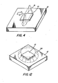
- Figure 4 shows in perspective view a single island on which is superimposed in phantom lines the spatial profile of the optical intensity of the laser spot.
- Figure 5 is a side elevation view of an island upon a substrate, wherein the thermal control structure of this invention has not been incorporated, showing thermal losses to the substrate during cooling as represented by arrows whose length and direction generally indicate the velocity of heat loss;
- Figure 6 is a side elevation view of a crystallizable island upon a substrate, showing tuning layers comprising one form of the thermal control structure of this invention and arrows indicating relative thermal losses to the substrate during cooling;
- Figure 7 is a side elevation view similar to Figure 6 showing a moat and sea arrangement comprising another form of the thermal control structure of this invention;
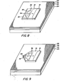
- Figure 8 shows in perspective view a single island with a sweeping molten zone and a single nucleation site at the center of its leading edge from which the crystallization front radiates;
- Figure 9 shows in perspective view similar to Figure 8 an alternative embodiment of island shape for enhanced control of nucleation;
- Figure 10 shows in perspective view the embodiment of Figure 7 including a moat and sea surrounding the single island, and also showing the single nucleation site, crystallization front and sweeping molten zone;
- Figure 11 shows in perspective view a modification of the Figure 10 embodiment showing a variation of the moat configuration for enhanced control of nucleation;
- Figure 12 is a perspective view of a single island on which is superimposed in phantom lines a profile of the optical intensity of a laser spot which heats the entire island and its immediate surround, simultaneously;
- Figure 13 shows in perspective view a single island shaped for enhanced control of nucleation when heating is accomplished in the manner of Figure 12;
- Figure 14 is an elevation view of still another embodiment of this invention showing an encapsulating layer in conjunction with the tuning layer configuration; and
- Figure 15 is an elevation view of yet another embodiment of this invention showing an encapsulating layer in conjunction with the moat and sea configuration.
- Turning now to the drawings, in greater detail, there is shown in Figure 1 an array of
silicon islands 10 disposed upon asuitable substrate 12. As deposited, the islands are in the amorphous or fine grain polycrystalline form. By the term island we mean, of course, a prepositioned pattern of areas to be converted. For example, a stripe is to be considered an island whose length to width ratio is exceedingly large. After being irradiated by sweepinglaser beam 14, moving in the direction of the arrow, each island is converted to a single crystal. An optical system (not shown) has been interposed between the laser source and the target to change the shape of the beam so that the laser "spot" 16 upon the target will be elongated, substantially as shown. A suitable scanning mechanism (also not shown) moves the "spot", relative to the island, in the direction of its short dimension, which is selected to be less than the island length in the direction of scan for incremental or zone heating of the island, while the long dimension is selected to exceed the island width for irradiating the immediately surroundingarea 18 . in order to accomplish the results of the instant invention. As it is desired to convert the islands into single crystalline material we have found that accurate heating and cooling of theislands 10 and itsimmediate surround 18 is important. - In Figure 2, laser irradiation of the island is shown to be sufficiently intense to form a
molten zone 19 within the island whose upper surface is seen to be convex. In theupsteam area 20, the cooled crystallized portion of the island is slightly thinner than thedownstream area 21 because of the mass transport of material in the molten zone. Upon passage of the laser spot and complete crystallization of. the island, the surface will be slightly rippled and a small ridge of transported material will reside at its end. - An intensity profile of the laser spot, as shown in schematic perspective in Figure 4, is seen to have a
distribution 22 which falls off rapidly in the direction of laser travel and is effectively uniform normal to the direction of laser travel. - i As the scanning laser spot moves, the mechanism of cooling occurs sequentially from the leading island edge onward. Thermal energy, accumulated in the
island 10 is lost to the cooler substrate. Lateral heat flow, which is negligible in all the thin layers, occurs within the substrate which is sufficiently thick to allow this phenomenon. We have shown in Figures 5, 6 and 7 schematic representations of thermal energy loss to the substrate from the laser heated areas, under several conditions. These illustrations provide an explanation of the instant invention. - In Figure 5, an island of amorphous or
polycrystalline semiconductor 10, such as silicon or germanium, which are known to absorb optical energy is disposed upon a substrate, such as glass, which is not optical energy absorbing. The island will be subject to optical energy irradiation from a scanning or pulsed laser, an infra-red source, a flash lamp or from any other suitable means with irradiation taking place in the zone between the dotted lines. Only the island will be heated, the exposed portions of the glass substrate surrounding the island will not absorb optical energy and will remain cool. Thus, when cooling of the island occurs, as shown by the arrows, the central portion of the island loses its heat directly into the glass substrate while the edge portions of the island lose heat more rapidly as thermal energy passes both downwardly and laterally outwardly into the cool substrate. - This heat flow pattern will result in cooler island edges at which plural nucleation locations will be established. As shown in Figure 4, a sweeping laser spot will leave the leading edge of the island cooler ' than the lateral edges. Thus, desirably, nucleation will be initiated at the leading edge and crystal growth will extend therefrom. However, in the Figure 5 situation nucleation can also be initiated at the lateral edges. Thus, competing crystallization fronts can radiate from several nucleation locations, resulting in a polycrystalline island.
- In order to suppress competing nucleation between that desired at the lead edge and that undesired at the lateral edges, we have determined that by elevating the temperature of the surrounding area, heat flow from the island lateral edges into the substrate may be accurately controlled to the extent necessary to suppress edge nucleation. By providing an optical energy absorbing layer upon the glass substrate and irradiating this composite structure with a suitable optical energy source, the island surround also will be heated. If an optical energy absorbing substrate us used, the uppermost portion thereof functions as if it were a separate optical energy absorbing layer. Thermal losses to the substrate in the vicinity of the island edges will be additive, including heat from both the surround and the island edges. Thus, the substrate will be hotter in the region of the lateral edges, resulting in a reduced rate of heat loss from the edges as compared to the central portion of the island. By controlling the amount of thermal input into the surrounding area, thermal loss to the substrate and the probability of edge nucleation can be controlled.
- For example, in the thermal control embodiment of Figure 6, an optical
energy absorbing layer 23 has been deposited upon anonabsorbing substrate 24. A pair of thin dielectric tuning layers 26 and 28overlay absorbing layer 23 for controlling (tuning) the amount of thermal input into the absorbing layer. When the heat source has been removed and the system cools, heat will flow downwardly, as shown, to the cooler substrate directly below the central portion of the island. But, at the lateral island edges, where thesurround 18 has also been heated, the optical absorbinglayer 23 also seeks to lose heat to the cooler substrate below the island. Thus, there are additive contributions of heat flow to the substrate in this area. The shorter diagonal arrows represent a slower resultant rate of heat loss at island edges than at the island center. In other words, a controlled thermal gradient exists between the central portion of the island and the lateral edges thereof. - Another thermal control embodiment is suggested in Figure 7 wherein a moat 30 (absence of optical energy absorbing layer) and a sea 32 (existence of optical energy absorbing layer) surround each island. Only one island is shown, but it is to be understood that each island is so surrounded. As in Figures 5 and 6, a suitable optical energy source had been projected upon the
island 10 and its immediate surounding area 18 (as shown by the dotted lines) to heat the optical absorbing layers, namely, the island and the sea. The substrate is not optically absorbing and, therefore, in the area of the moat it will remain relatively cool. The heated sea and the heated island edge areas combine to lose their accumulated heat to the cooler substrate in the moat area. Thus, the island edges will be warmer and the thermal gradient between the island edges and their associated substrate will be smaller than the similar situation without a thermal control structure (as in Figure 5). The resultant slower edge cooling (warmer edge area) suppresses the formation of nucleation locations at the edges. - The key to success in growing large area single crystal islands on a suitable substrate has been found to be a combination of suppression of competitive nucleation as described, and enhanced control of nucleation and growth from a single seed.
- In Figures 8-11 single crystal growth is shown in several embodiments. Lateral thermal flow according to that described with regard to Figure 6 takes place in the embodiments of Figures 8 and 9 while lateral thermal flow as shown in Figure 7 takes place in the Figures 10 and 11 embodiments. In each, laser scanning takes place with a laser spot substantially as shown at 14 in Figure 1, having an optical profile as shown at 22 in Figure 4.
- In Figure 8 the scanning laser spot moving over the island and its surrounding area, zone melts the island as shown at 19. It should be noted that the molten zone is seen to flare outwardly at the lateral edges due to the increased heat thereat. As the molten zone passes the island leading edge, its trailing edge will cool first and crystallization will begin. A
nucleation site 34 will form, from which acrystallization front 36 radiates. We have found that althoughplural crystallization sites 35 are sometimes present on the leading edge one site generally establishes a dominant front. As fully explained above it is the intent of this invention to support a single crystallization front while suppressing competitive nucleation sites at the lateral island edges. This has been accomplished by reducing the rate of thermal flow from the edges, thereby maintaining the edges hot enough to prevent spontaneous nucleation. An improved island configuration 10' is shown in Figure 9 wherein a tapered shape at the leading edge enhances self-seeding from asingle point 38. This substantially eliminates the possibility of plural nucleation sites at the leading edge. - In Figures 10 and 11 the moat configuration is shown in perspective for a better visual understanding of the system. Both figures illustrate nucleation of a single crystal and the crystal front propagating therefrom. In Figure 10 a
rectangular moat 30 encircles a rectangular island. Leading edge nucleation occurs in a manner similar to that described with reference to Figure 8. In Figure 11 the moat has been tapered at 40 in advance of the island leading edge to enhance cooling at the center of the island leading edge. - While describing the heating process of this invention as one of zone melting, it should be understood that our invention also comprehends heating the entire island and its immediate surrounding area, or plural islands and their surround, with a single, pulsed, large optical energy source. The mechanism of seeding and crystal growth described above also will be carried out in this form of the invention. Figures 12 and 13 are of note with respect to this means of heating. In Figure 12, the optical intensity profile of a large area laser pulse is shown in phantom lines at 39 as being effectively uniform over the
island 10 and falling off rapidly in the surround. Figure 13 illustrates an example of anotherisland configuration 10" disposed upon a single dielectric thermal control layer, wherein the surround is hotter than the island under uniform illumination. In this mode, theinterior point 42 will be heated less than the other exterior island points and will act as the nucleation center. - I Now that the physical principles have been set forth, several examples of the parameters and materials utilized in our experiments shall be described. In the Figure 8 configuration, the
substrate 24 was made of silica (Si02) a non-optical energy absorbing material upon which was disposed an optical absorbinglayer 23 comprising a 1 /um CVD deposited polysilicon which in turn supported an 88 nm thermally growndielectric oxide layer 26 over which was added a second thin dielectric layer comprising 64 nm of CVD deposited silicon nitride (Si3N4).Islands 10 of 0.5 /um thick CVD deposited polysilicon (also optical energy absorbing) over the nitride layer were photolithographically produced. A CW argon ion laser having a wavelength of 5145 A was formed into a collimated elliptical beam (with a ratio of diameters equal to three) and focused to a spot approximately 30 µm x 90 /um. This spot was scanned in a direction normal to its wide dimension at 1 cm/sec over the central axes of the deposited islands so that the islands achieved a melting temperature of 1412°C. After laser scanning, the islands were studied in a TEM where it was observed thatislands 20/um wide by 20 µm long with no grain boundaries were present. We also observed the black body radiation from the laser heated area during annealing to confirm our analysis of the thermal control mechanism., - In order to optimally control the thermal input to the polysilicon optical absorbing layer and then to the island edges, as explained above, we have experimented with a dual dielectric (Si02 and Si3N4) overcoating of various thicknesses and therefore various reflectivities to obtain the optimal thermal tuning. Since the area surrounding the island is reflectively coated and the polysilicon island is uncoated, the surround will absorb less thermal energy than the island. We have also experimented with a single dielectric layer upon the optical absorbing layer, namely, the 88 nm oxide layer alone but as this configuration is maximally absorbing (nonreflecting) the surround absorbs more optical energy than the uncoated islands resulting in a net heat influx to the islands. Edge heating in this instance appears to be undesirably strong. Although this single dielectric embodiment will yield the desired results it is not altogether satisfactory to maximize the lateral edge thermal profile because substrate damage due to extreme heating is possible. Since we seek to obtain the desired results with minimum heating of the .substrate the dual dielectric tuning has been found to be preferable.
- The configuration of Figures 10 and 11 is much simpler from a processing point of view. During fabrication of the fine grain polysilicon islands, instead of photolithographically stripping away the entire surrounding material between islands, only a
moat 30 is removed. We have found that a, moat of approximately 4 um wide will be satisfactory. The thermal flow dynamics of this configuration have already been described. Suffice it to state that the moat is considered to be a control structure which provides an unheated zone in the nonabsorbing substrate which accepts heat from both the sea and from the island perimeter. This thermal addition moderates rapid heat loss from the island perimeter and slows formation of nucleation centers. After the laser annealing process has been completed, the surrounding sea material may be removed for device processing, or partially left as laser annealed coarse grained polysilicon connectors. - In Figures 14 and 15 we suggest the solution to a further problem, namely, that of retaining a smooth top surface on the islands after laser induced melting and recrystallization- The effects of surface tension and mass transport during melting have been observed to produce substantial thickness variations. For example, for the slow laser scan described (i.e. 1 cm/sec) the molten zone in a bare island is a convex, surface tension determined, ridge (see 19 in Figure 2). Further, shock driven ripples quench into the solidifying topography and mass transport occurs to the trailing edge of the island. We have found that an
encapsulating layer 43 retains the smooth upper surface of the island after laser annealing by preventing the surface deformation effects. In Figure 14 a dielectric thin film such as Si02 or Si3N4, approximately 20 nm thick deposited over the amorphous or polycrystalline silicon islands and the area surrounding the islands will serve the dual function of encapsulation for topographic integrity and control of thermal energy acceptance by the optical absorbingmaterial 23 in conjunction with afirst dielectric layer 26 upon which it'is deposited. Also, the single dielectric layer over the island will enhance the transmission of optical energy into the island (thus requiring less incident energy) and, because the dielectric melts at a higher temperature than silicon it will also suppress island ablation. Thus, the molten region can be forced to a higher temperature to improve crystal growth. In Figure 15, thedielectric overlayer 44 is combined with the sea and moat embodiment to perform the same enhancing results described with reference to Figure 14.
Claims (10)
Applications Claiming Priority (2)
| Application Number | Priority Date | Filing Date | Title |
|---|---|---|---|
| US182195 | 1980-08-28 | ||
| US06/182,195 US4330363A (en) | 1980-08-28 | 1980-08-28 | Thermal gradient control for enhanced laser induced crystallization of predefined semiconductor areas |
Publications (3)
| Publication Number | Publication Date |
|---|---|
| EP0047140A2 true EP0047140A2 (en) | 1982-03-10 |
| EP0047140A3 EP0047140A3 (en) | 1984-10-17 |
| EP0047140B1 EP0047140B1 (en) | 1986-11-05 |
Family
ID=22667420
Family Applications (1)
| Application Number | Title | Priority Date | Filing Date |
|---|---|---|---|
| EP81303924A Expired EP0047140B1 (en) | 1980-08-28 | 1981-08-27 | Method of converting areas of semiconductor material into single crystal areas |
Country Status (5)
| Country | Link |
|---|---|
| US (1) | US4330363A (en) |
| EP (1) | EP0047140B1 (en) |
| JP (1) | JPS5772319A (en) |
| CA (1) | CA1157167A (en) |
| DE (1) | DE3175577D1 (en) |
Cited By (10)
| Publication number | Priority date | Publication date | Assignee | Title |
|---|---|---|---|---|
| EP0127323A1 (en) * | 1983-04-30 | 1984-12-05 | Fujitsu Limited | A process for producing a single crystal semiconductor island on an insulator |
| EP0154373A1 (en) * | 1984-02-21 | 1985-09-11 | Koninklijke Philips Electronics N.V. | Methods for producing single crystals in insulators |
| EP0178447A2 (en) * | 1984-10-09 | 1986-04-23 | Fujitsu Limited | A manufacturing method of an integrated circuit based on semiconductor-on-insulator technology |
| DE3921038A1 (en) * | 1988-06-28 | 1990-01-04 | Ricoh Kk | Semiconductor substrate and method of fabrication thereof |
| US5173446A (en) * | 1988-06-28 | 1992-12-22 | Ricoh Company, Ltd. | Semiconductor substrate manufacturing by recrystallization using a cooling medium |
| US5310446A (en) * | 1990-01-10 | 1994-05-10 | Ricoh Company, Ltd. | Method for producing semiconductor film |
| US5459346A (en) * | 1988-06-28 | 1995-10-17 | Ricoh Co., Ltd. | Semiconductor substrate with electrical contact in groove |
| US7229861B2 (en) | 1994-09-16 | 2007-06-12 | Semiconductor Energy Laboratory Co., Ltd. | Method for producing semiconductor device |
| US7279372B2 (en) | 2001-12-11 | 2007-10-09 | Semiconductor Energy Laboratory Co., Ltd. | Manufacturing method of semiconductor device |
| US7393729B2 (en) | 2001-08-17 | 2008-07-01 | Semiconductor Energy Laboratory Co., Ltd. | Method for fabricating semiconductor device |
Families Citing this family (135)
| Publication number | Priority date | Publication date | Assignee | Title |
|---|---|---|---|---|
| US5302230A (en) * | 1980-02-27 | 1994-04-12 | Ricoh Company, Ltd. | Heat treatment by light irradiation |
| JPS5734331A (en) * | 1980-08-11 | 1982-02-24 | Toshiba Corp | Manufacture of semiconductor device |
| GB2106419B (en) * | 1981-02-04 | 1984-08-15 | Western Electric Co | Growth of structures based on group iv semiconductor materials |
| US4406709A (en) * | 1981-06-24 | 1983-09-27 | Bell Telephone Laboratories, Incorporated | Method of increasing the grain size of polycrystalline materials by directed energy-beams |
| JPS5821319A (en) * | 1981-07-30 | 1983-02-08 | Fujitsu Ltd | Annealing by laser |
| JPS5861622A (en) * | 1981-10-09 | 1983-04-12 | Hitachi Ltd | Manufacture of single crystal thin film |
| US4388145A (en) * | 1981-10-29 | 1983-06-14 | Xerox Corporation | Laser annealing for growth of single crystal semiconductor areas |
| JPS58115832A (en) * | 1981-12-28 | 1983-07-09 | Fujitsu Ltd | Manufacture of semiconductor device |
| JPS58164219A (en) * | 1982-03-25 | 1983-09-29 | Agency Of Ind Science & Technol | Manufacture of laminated semiconductor device |
| JPS58194799A (en) * | 1982-05-07 | 1983-11-12 | Hitachi Ltd | Preparation of silicon single crystal |
| US4562106A (en) * | 1982-06-23 | 1985-12-31 | Massachusetts Institute Of Technology | Product made by method of entraining dislocations and other crystalline defects |
| US4479846A (en) * | 1982-06-23 | 1984-10-30 | Massachusetts Institute Of Technology | Method of entraining dislocations and other crystalline defects in heated film contacting patterned region |
| US4536231A (en) * | 1982-10-19 | 1985-08-20 | Harris Corporation | Polysilicon thin films of improved electrical uniformity |
| JPS59119718A (en) * | 1982-12-27 | 1984-07-11 | Toshiba Corp | Growth method of thin-film single crystal |
| US4592799A (en) * | 1983-05-09 | 1986-06-03 | Sony Corporation | Method of recrystallizing a polycrystalline, amorphous or small grain material |
| JPS59229815A (en) * | 1983-06-13 | 1984-12-24 | Hitachi Ltd | Manufacture of semiconductor substrate |
| US4853076A (en) * | 1983-12-29 | 1989-08-01 | Massachusetts Institute Of Technology | Semiconductor thin films |
| US4585512A (en) * | 1984-01-27 | 1986-04-29 | Sony Corporation | Method for making seed crystals for single-crystal semiconductor devices |
| JPS60213018A (en) * | 1984-04-09 | 1985-10-25 | Hitachi Ltd | Semiconductor substrate |
| US4536251A (en) * | 1984-06-04 | 1985-08-20 | Xerox Corporation | Method for eliminating laser-induced substrate fissures associated with crystallized silicon areas |
| US4598305A (en) * | 1984-06-18 | 1986-07-01 | Xerox Corporation | Depletion mode thin film semiconductor photodetectors |
| US4737233A (en) * | 1984-10-22 | 1988-04-12 | American Telephone And Telegraph Company, At&T Bell Laboratories | Method for making semiconductor crystal films |
| US5753542A (en) | 1985-08-02 | 1998-05-19 | Semiconductor Energy Laboratory Co., Ltd. | Method for crystallizing semiconductor material without exposing it to air |
| US4654090A (en) * | 1985-09-13 | 1987-03-31 | Xerox Corporation | Selective disordering of well structures by laser annealing |
| USRE33274E (en) * | 1985-09-13 | 1990-07-24 | Xerox Corporation | Selective disordering of well structures by laser annealing |
| JPH084067B2 (en) * | 1985-10-07 | 1996-01-17 | 工業技術院長 | Method for manufacturing semiconductor device |
| EP0235819B1 (en) * | 1986-03-07 | 1992-06-10 | Iizuka, Kozo | Process for producing single crystal semiconductor layer |
| US4771010A (en) * | 1986-11-21 | 1988-09-13 | Xerox Corporation | Energy beam induced layer disordering (EBILD) |
| US4743567A (en) * | 1987-08-11 | 1988-05-10 | North American Philips Corp. | Method of forming thin, defect-free, monocrystalline layers of semiconductor materials on insulators |
| US5453153A (en) * | 1987-11-13 | 1995-09-26 | Kopin Corporation | Zone-melting recrystallization process |
| US5021119A (en) * | 1987-11-13 | 1991-06-04 | Kopin Corporation | Zone-melting recrystallization process |
| US4885052A (en) * | 1987-11-13 | 1989-12-05 | Kopin Corporation | Zone-melting recrystallization process |
| US4888302A (en) * | 1987-11-25 | 1989-12-19 | North American Philips Corporation | Method of reduced stress recrystallization |
| JPH0633218B2 (en) * | 1987-12-08 | 1994-05-02 | 日本鋼管株式会社 | Silicon single crystal manufacturing equipment |
| DE69125886T2 (en) * | 1990-05-29 | 1997-11-20 | Semiconductor Energy Lab | Thin film transistors |
| JP3213338B2 (en) * | 1991-05-15 | 2001-10-02 | 株式会社リコー | Manufacturing method of thin film semiconductor device |
| US6975296B1 (en) * | 1991-06-14 | 2005-12-13 | Semiconductor Energy Laboratory Co., Ltd. | Electro-optical device and method of driving the same |
| US5329207A (en) * | 1992-05-13 | 1994-07-12 | Micron Technology, Inc. | Field emission structures produced on macro-grain polysilicon substrates |
| TW369686B (en) * | 1993-07-27 | 1999-09-11 | Semiconductor Energy Lab Corp | Semiconductor device and process for fabricating the same |
| US6884698B1 (en) * | 1994-02-23 | 2005-04-26 | Semiconductor Energy Laboratory Co., Ltd. | Method for manufacturing semiconductor device with crystallization of amorphous silicon |
| KR100321541B1 (en) * | 1994-03-09 | 2002-06-20 | 야마자끼 순페이 | How Active Matrix Display Devices Work |
| US6723590B1 (en) * | 1994-03-09 | 2004-04-20 | Semiconductor Energy Laboratory Co., Ltd. | Method for laser-processing semiconductor device |
| TW280037B (en) * | 1994-04-22 | 1996-07-01 | Handotai Energy Kenkyusho Kk | Drive circuit of active matrix type display device and manufacturing method |
| JP3897826B2 (en) * | 1994-08-19 | 2007-03-28 | 株式会社半導体エネルギー研究所 | Active matrix display device |
| US5712191A (en) * | 1994-09-16 | 1998-01-27 | Semiconductor Energy Laboratory Co., Ltd. | Method for producing semiconductor device |
| JP3469337B2 (en) * | 1994-12-16 | 2003-11-25 | 株式会社半導体エネルギー研究所 | Method for manufacturing semiconductor device |
| JP3778456B2 (en) | 1995-02-21 | 2006-05-24 | 株式会社半導体エネルギー研究所 | Method for manufacturing insulated gate thin film semiconductor device |
| TW297138B (en) * | 1995-05-31 | 1997-02-01 | Handotai Energy Kenkyusho Kk | |
| US6790714B2 (en) * | 1995-07-03 | 2004-09-14 | Sanyo Electric Co., Ltd. | Semiconductor device, display device and method of fabricating the same |
| US6444506B1 (en) * | 1995-10-25 | 2002-09-03 | Semiconductor Energy Laboratory Co., Ltd. | Method of manufacturing silicon thin film devices using laser annealing in a hydrogen mixture gas followed by nitride formation |
| KR100514417B1 (en) * | 1995-12-26 | 2005-12-20 | 세이코 엡슨 가부시키가이샤 | Active Matrix Substrate, Active Matrix Substrate Manufacturing Method, Liquid Crystal Display and Electronic Devices |
| JP3645378B2 (en) | 1996-01-19 | 2005-05-11 | 株式会社半導体エネルギー研究所 | Method for manufacturing semiconductor device |
| JP3645379B2 (en) | 1996-01-19 | 2005-05-11 | 株式会社半導体エネルギー研究所 | Method for manufacturing semiconductor device |
| JP3729955B2 (en) * | 1996-01-19 | 2005-12-21 | 株式会社半導体エネルギー研究所 | Method for manufacturing semiconductor device |
| US6478263B1 (en) * | 1997-01-17 | 2002-11-12 | Semiconductor Energy Laboratory Co., Ltd. | Semiconductor device and its manufacturing method |
| JP3645380B2 (en) * | 1996-01-19 | 2005-05-11 | 株式会社半導体エネルギー研究所 | Manufacturing method of semiconductor device, information terminal, head mounted display, navigation system, mobile phone, video camera, projection display device |
| US5888858A (en) | 1996-01-20 | 1999-03-30 | Semiconductor Energy Laboratory Co., Ltd. | Semiconductor device and fabrication method thereof |
| US6180439B1 (en) * | 1996-01-26 | 2001-01-30 | Semiconductor Energy Laboratory Co., Ltd. | Method for fabricating a semiconductor device |
| US7056381B1 (en) * | 1996-01-26 | 2006-06-06 | Semiconductor Energy Laboratory Co., Ltd. | Fabrication method of semiconductor device |
| US6465287B1 (en) | 1996-01-27 | 2002-10-15 | Semiconductor Energy Laboratory Co., Ltd. | Method for fabricating a semiconductor device using a metal catalyst and high temperature crystallization |
| US6100562A (en) | 1996-03-17 | 2000-08-08 | Semiconductor Energy Laboratory Co., Ltd. | Method of manufacturing a semiconductor device |
| US5893948A (en) * | 1996-04-05 | 1999-04-13 | Xerox Corporation | Method for forming single silicon crystals using nucleation sites |
| DE19651003C2 (en) * | 1996-11-29 | 2001-10-25 | Hahn Meitner Inst Berlin Gmbh | Process for the production of a flat single crystal on a foreign substrate |
| JP4112655B2 (en) * | 1997-09-25 | 2008-07-02 | 東芝松下ディスプレイテクノロジー株式会社 | Method for producing polycrystalline thin film |
| KR100269312B1 (en) * | 1997-10-14 | 2000-10-16 | 윤종용 | Method for crystallization of silicon film and fabricating method for thin film transistor-liquid crystal display using the same |
| JPH11214700A (en) | 1998-01-23 | 1999-08-06 | Semiconductor Energy Lab Co Ltd | Semiconductor display device |
| JPH11338439A (en) | 1998-03-27 | 1999-12-10 | Semiconductor Energy Lab Co Ltd | Driving circuit of semiconductor display device and semiconductor display device |
| JP3844613B2 (en) | 1998-04-28 | 2006-11-15 | 株式会社半導体エネルギー研究所 | Thin film transistor circuit and display device using the same |
| GB9819338D0 (en) * | 1998-09-04 | 1998-10-28 | Philips Electronics Nv | Laser crystallisation of thin films |
| JP2000111950A (en) * | 1998-10-06 | 2000-04-21 | Toshiba Corp | Manufacture of polycrystalline silicon |
| EP1076359B1 (en) * | 1999-08-13 | 2011-02-23 | Semiconductor Energy Laboratory Co., Ltd. | Laser irradiation device |
| US6573162B2 (en) * | 1999-12-24 | 2003-06-03 | Semiconductor Energy Laboratory Co., Ltd. | Laser irradiation apparatus and method of fabricating a semiconductor device |
| US6780687B2 (en) * | 2000-01-28 | 2004-08-24 | Semiconductor Energy Laboratory Co., Ltd. | Method of manufacturing a semiconductor device having a heat absorbing layer |
| US6856630B2 (en) * | 2000-02-02 | 2005-02-15 | Semiconductor Energy Laboratory Co., Ltd. | Beam homogenizer, laser irradiation apparatus, semiconductor device, and method of fabricating the semiconductor device |
| US6872607B2 (en) * | 2000-03-21 | 2005-03-29 | Semiconductor Energy Laboratory Co., Ltd. | Method of manufacturing a semiconductor device |
| DE10042733A1 (en) * | 2000-08-31 | 2002-03-28 | Inst Physikalische Hochtech Ev | Multicrystalline laser-crystallized silicon thin-film solar cell on a transparent substrate |
| US6831299B2 (en) * | 2000-11-09 | 2004-12-14 | Semiconductor Energy Laboratory Co., Ltd. | Semiconductor device |
| TWI313059B (en) * | 2000-12-08 | 2009-08-01 | Sony Corporatio | |
| SG113399A1 (en) | 2000-12-27 | 2005-08-29 | Semiconductor Energy Lab | Laser annealing method and semiconductor device fabricating method |
| SG118117A1 (en) * | 2001-02-28 | 2006-01-27 | Semiconductor Energy Lab | Semiconductor device and manufacturing method thereof |
| TW558861B (en) * | 2001-06-15 | 2003-10-21 | Semiconductor Energy Lab | Laser irradiation stage, laser irradiation optical system, laser irradiation apparatus, laser irradiation method, and method of manufacturing semiconductor device |
| US6692999B2 (en) * | 2001-06-26 | 2004-02-17 | Fujitsu Limited | Polysilicon film forming method |
| US6770546B2 (en) * | 2001-07-30 | 2004-08-03 | Semiconductor Energy Laboratory Co., Ltd. | Method of manufacturing semiconductor device |
| US6596077B2 (en) | 2001-07-31 | 2003-07-22 | Illinois Institute Of Technology | Controlled nucleation of protein crystals |
| US6733586B2 (en) | 2001-07-31 | 2004-05-11 | Illinois Institute Of Technology | High throughput non-photochemical laser induced nucleation |
| TW552645B (en) * | 2001-08-03 | 2003-09-11 | Semiconductor Energy Lab | Laser irradiating device, laser irradiating method and manufacturing method of semiconductor device |
| US6847006B2 (en) * | 2001-08-10 | 2005-01-25 | Semiconductor Energy Laboratory Co., Ltd. | Laser annealing apparatus and semiconductor device manufacturing method |
| TWI282126B (en) * | 2001-08-30 | 2007-06-01 | Semiconductor Energy Lab | Method for manufacturing semiconductor device |
| US7112517B2 (en) | 2001-09-10 | 2006-09-26 | Semiconductor Energy Laboratory Co., Ltd. | Laser treatment device, laser treatment method, and semiconductor device fabrication method |
| US7317205B2 (en) * | 2001-09-10 | 2008-01-08 | Semiconductor Energy Laboratory Co., Ltd. | Light emitting device and method of manufacturing a semiconductor device |
| JP4397571B2 (en) | 2001-09-25 | 2010-01-13 | 株式会社半導体エネルギー研究所 | Laser irradiation method, laser irradiation apparatus, and manufacturing method of semiconductor device |
| US6700096B2 (en) * | 2001-10-30 | 2004-03-02 | Semiconductor Energy Laboratory Co., Ltd. | Laser apparatus, laser irradiation method, manufacturing method for semiconductor device, semiconductor device, production system for semiconductor device using the laser apparatus, and electronic equipment |
| SG108878A1 (en) * | 2001-10-30 | 2005-02-28 | Semiconductor Energy Lab | Laser irradiation method and laser irradiation apparatus, and method for fabricating semiconductor device |
| TWI289896B (en) * | 2001-11-09 | 2007-11-11 | Semiconductor Energy Lab | Laser irradiation apparatus, laser irradiation method, and method of manufacturing a semiconductor device |
| US6962860B2 (en) * | 2001-11-09 | 2005-11-08 | Semiconductor Energy Laboratory Co., Ltd. | Method of manufacturing a semiconductor device |
| TWI291729B (en) | 2001-11-22 | 2007-12-21 | Semiconductor Energy Lab | A semiconductor fabricating apparatus |
| JP2003224070A (en) * | 2001-11-26 | 2003-08-08 | Semiconductor Energy Lab Co Ltd | Method for manufacturing semiconductor device |
| US7105048B2 (en) * | 2001-11-30 | 2006-09-12 | Semiconductor Energy Laboratory Co., Ltd. | Laser irradiation apparatus |
| KR100967824B1 (en) * | 2001-11-30 | 2010-07-05 | 가부시키가이샤 한도오따이 에네루기 켄큐쇼 | Manufacturing method for a semiconductor device |
| JP3934536B2 (en) * | 2001-11-30 | 2007-06-20 | 株式会社半導体エネルギー研究所 | Laser irradiation apparatus, laser irradiation method, and manufacturing method of semiconductor device |
| US7133737B2 (en) * | 2001-11-30 | 2006-11-07 | Semiconductor Energy Laboratory Co., Ltd. | Program for controlling laser apparatus and recording medium for recording program for controlling laser apparatus and capable of being read out by computer |
| US7214573B2 (en) * | 2001-12-11 | 2007-05-08 | Semiconductor Energy Laboratory Co., Ltd. | Method of manufacturing a semiconductor device that includes patterning sub-islands |
| US7135389B2 (en) * | 2001-12-20 | 2006-11-14 | Semiconductor Energy Laboratory Co., Ltd. | Irradiation method of laser beam |
| JP4141138B2 (en) * | 2001-12-21 | 2008-08-27 | 株式会社半導体エネルギー研究所 | Method for manufacturing semiconductor device |
| JP3992976B2 (en) * | 2001-12-21 | 2007-10-17 | 株式会社半導体エネルギー研究所 | Method for manufacturing semiconductor device |
| JP2003204067A (en) * | 2001-12-28 | 2003-07-18 | Semiconductor Energy Lab Co Ltd | Display device and electronic equipment using the same |
| JP4011344B2 (en) * | 2001-12-28 | 2007-11-21 | 株式会社半導体エネルギー研究所 | Method for manufacturing semiconductor device |
| JP4030758B2 (en) | 2001-12-28 | 2008-01-09 | 株式会社半導体エネルギー研究所 | Method for manufacturing semiconductor device |
| EP1326273B1 (en) * | 2001-12-28 | 2012-01-18 | Semiconductor Energy Laboratory Co., Ltd. | Semiconductor device |
| US6933527B2 (en) | 2001-12-28 | 2005-08-23 | Semiconductor Energy Laboratory Co., Ltd. | Semiconductor device and semiconductor device production system |
| US6841797B2 (en) * | 2002-01-17 | 2005-01-11 | Semiconductor Energy Laboratory Co., Ltd. | Semiconductor device formed over a surface with a drepession portion and a projection portion |
| TW200302511A (en) | 2002-01-28 | 2003-08-01 | Semiconductor Energy Lab | Semiconductor device and method of manufacturing the same |
| TWI261358B (en) * | 2002-01-28 | 2006-09-01 | Semiconductor Energy Lab | Semiconductor device and method of manufacturing the same |
| US7749818B2 (en) * | 2002-01-28 | 2010-07-06 | Semiconductor Energy Laboratory Co., Ltd. | Semiconductor device and method of manufacturing the same |
| JP4137460B2 (en) * | 2002-02-08 | 2008-08-20 | 株式会社半導体エネルギー研究所 | Method for manufacturing semiconductor device |
| KR100979926B1 (en) * | 2002-03-05 | 2010-09-03 | 가부시키가이샤 한도오따이 에네루기 켄큐쇼 | Semiconductor element and semiconductor device using the same |
| US6847050B2 (en) * | 2002-03-15 | 2005-01-25 | Semiconductor Energy Laboratory Co., Ltd. | Semiconductor element and semiconductor device comprising the same |
| US6841434B2 (en) * | 2002-03-26 | 2005-01-11 | Semiconductor Energy Laboratory Co., Ltd. | Method of fabricating semiconductor device |
| US6930326B2 (en) * | 2002-03-26 | 2005-08-16 | Semiconductor Energy Laboratory Co., Ltd. | Semiconductor circuit and method of fabricating the same |
| US6984573B2 (en) * | 2002-06-14 | 2006-01-10 | Semiconductor Energy Laboratory Co., Ltd. | Laser irradiation method and apparatus |
| JP4532058B2 (en) * | 2002-08-26 | 2010-08-25 | 日本発條株式会社 | Correction method, correction device, and correction program |
| JP4282985B2 (en) * | 2002-12-27 | 2009-06-24 | 株式会社半導体エネルギー研究所 | Method for manufacturing display device |
| US7397592B2 (en) * | 2003-04-21 | 2008-07-08 | Semiconductor Energy Laboratory Co., Ltd. | Beam irradiation apparatus, beam irradiation method, and method for manufacturing a thin film transistor |
| US7476629B2 (en) * | 2003-04-21 | 2009-01-13 | Semiconductor Energy Laboratory Co., Ltd. | Beam irradiation apparatus, beam irradiation method, and method for manufacturing thin film transistor |
| US7220627B2 (en) * | 2003-04-21 | 2007-05-22 | Semiconductor Energy Laboratory Co., Ltd. | Method for manufacturing a semiconductor device where the scanning direction changes between regions during crystallization and process |
| TW594884B (en) * | 2003-05-29 | 2004-06-21 | Univ Nat Chiao Tung | Laser re-crystallization method of low temperature polysilicon thin film transistor |
| US7115449B2 (en) * | 2003-06-24 | 2006-10-03 | National Chiao Tung University | Method for fabrication of polycrystalline silicon thin film transistors |
| CA2537636A1 (en) * | 2003-09-03 | 2005-03-10 | Shmuel Bukshpan | Methods and apparatus for rapid crystallization of biomolecules |
| JP2009135453A (en) * | 2007-10-30 | 2009-06-18 | Semiconductor Energy Lab Co Ltd | Method for manufacturing semiconductor device, semiconductor device, and electronic device |
| US8334194B2 (en) * | 2008-02-06 | 2012-12-18 | Motech Americas, Llc | Methods and apparatus for manufacturing semiconductor wafers |
| JP5091730B2 (en) * | 2008-03-14 | 2012-12-05 | 株式会社日立製作所 | Method for manufacturing image display device using thin film semiconductor device |
| US20090280336A1 (en) * | 2008-05-08 | 2009-11-12 | Ralf Jonczyk | Semiconductor sheets and methods of fabricating the same |
| US10115654B2 (en) | 2010-06-18 | 2018-10-30 | Palo Alto Research Center Incorporated | Buried thermally conductive layers for heat extraction and shielding |
| US9356171B2 (en) * | 2012-01-25 | 2016-05-31 | The Trustees Of Dartmouth College | Method of forming single-crystal semiconductor layers and photovaltaic cell thereon |
| US9065009B2 (en) | 2012-04-10 | 2015-06-23 | First Solar, Inc. | Apparatus and method for forming a transparent conductive oxide layer over a substrate using a laser |
Family Cites Families (8)
| Publication number | Priority date | Publication date | Assignee | Title |
|---|---|---|---|---|
| US3335038A (en) * | 1964-03-30 | 1967-08-08 | Ibm | Methods of producing single crystals on polycrystalline substrates and devices using same |
| US3348962A (en) * | 1964-08-13 | 1967-10-24 | Hughes Aircraft Co | Method and apparatus for preparing single crystal thin films |
| US3549432A (en) * | 1968-07-15 | 1970-12-22 | Texas Instruments Inc | Multilayer microelectronic circuitry techniques |
| US3585088A (en) * | 1968-10-18 | 1971-06-15 | Ibm | Methods of producing single crystals on supporting substrates |
| US3600237A (en) * | 1969-12-17 | 1971-08-17 | Us Navy | Controlled nucleation in zone recrystallized insb films |
| US3737739A (en) * | 1971-02-22 | 1973-06-05 | Ibm | Single crystal regions in dielectric substrate |
| US3764776A (en) * | 1972-02-28 | 1973-10-09 | Emerson Electric Co | Method of making coherent shape of silicon carbide |
| US4199397A (en) * | 1976-02-09 | 1980-04-22 | Motorola, Inc. | Spontaneous growth of large crystal semiconductor material by controlled melt perturbation |
-
1980
- 1980-08-28 US US06/182,195 patent/US4330363A/en not_active Expired - Lifetime
-
1981
- 1981-06-22 CA CA000380341A patent/CA1157167A/en not_active Expired
- 1981-08-20 JP JP56130836A patent/JPS5772319A/en active Pending
- 1981-08-27 EP EP81303924A patent/EP0047140B1/en not_active Expired
- 1981-08-27 DE DE8181303924T patent/DE3175577D1/en not_active Expired
Non-Patent Citations (3)
| Title |
|---|
| APPLIED PHYSICS LETTERS, vol. 36, no. 11, 1st June 1980, pages 914-915, American Institute of Physics, New York, US; A.B. FOWLER et al.: "Selective laser annealing" * |
| APPLIED PHYSICS LETTERS, vol. 38, no. 3, 1st February 1981, pages 150-152, American Institute of Physics, New York, US; D.K. BIEGELSEN et al.: "Laser-induced crystallization of silicon islands on amorphous substrates: multilayer structures" * |
| IEEE TRANSACTIONS ON ELECTRON DEVICES, vol. ED-27, no. 3, March 1980, pages 573-578, IEEE, New York, US; G. YARON et al.: "LASOS-laser annealed silicon on sapphire" * |
Cited By (16)
| Publication number | Priority date | Publication date | Assignee | Title |
|---|---|---|---|---|
| US4543133A (en) * | 1983-04-30 | 1985-09-24 | Fujitsu Limited | Process for producing single crystalline semiconductor island on insulator |
| EP0127323A1 (en) * | 1983-04-30 | 1984-12-05 | Fujitsu Limited | A process for producing a single crystal semiconductor island on an insulator |
| EP0154373A1 (en) * | 1984-02-21 | 1985-09-11 | Koninklijke Philips Electronics N.V. | Methods for producing single crystals in insulators |
| EP0178447A2 (en) * | 1984-10-09 | 1986-04-23 | Fujitsu Limited | A manufacturing method of an integrated circuit based on semiconductor-on-insulator technology |
| EP0178447A3 (en) * | 1984-10-09 | 1988-02-03 | Fujitsu Limited | A manufacturing method of an integrated circuit based on the semiconductor-on-insulator technology and a device so manufactured |
| US5077233A (en) * | 1984-10-09 | 1991-12-31 | Fujitsu Limited | Method for recrystallizing specified portions of a non-crystalline semiconductor material to fabricate a semiconductor device therein |
| DE3921038C2 (en) * | 1988-06-28 | 1998-12-10 | Ricoh Kk | Method for producing a semiconductor substrate or solid structure |
| DE3921038A1 (en) * | 1988-06-28 | 1990-01-04 | Ricoh Kk | Semiconductor substrate and method of fabrication thereof |
| US5173446A (en) * | 1988-06-28 | 1992-12-22 | Ricoh Company, Ltd. | Semiconductor substrate manufacturing by recrystallization using a cooling medium |
| US5459346A (en) * | 1988-06-28 | 1995-10-17 | Ricoh Co., Ltd. | Semiconductor substrate with electrical contact in groove |
| US5565697A (en) * | 1988-06-28 | 1996-10-15 | Ricoh Company, Ltd. | Semiconductor structure having island forming grooves |
| US5310446A (en) * | 1990-01-10 | 1994-05-10 | Ricoh Company, Ltd. | Method for producing semiconductor film |
| US7229861B2 (en) | 1994-09-16 | 2007-06-12 | Semiconductor Energy Laboratory Co., Ltd. | Method for producing semiconductor device |
| US7393729B2 (en) | 2001-08-17 | 2008-07-01 | Semiconductor Energy Laboratory Co., Ltd. | Method for fabricating semiconductor device |
| US7279372B2 (en) | 2001-12-11 | 2007-10-09 | Semiconductor Energy Laboratory Co., Ltd. | Manufacturing method of semiconductor device |
| US7670935B2 (en) | 2001-12-11 | 2010-03-02 | Semiconductor Energy Laboratory Co., Ltd. | Manufacturing method of semiconductor device |
Also Published As
| Publication number | Publication date |
|---|---|
| CA1157167A (en) | 1983-11-15 |
| JPS5772319A (en) | 1982-05-06 |
| EP0047140B1 (en) | 1986-11-05 |
| DE3175577D1 (en) | 1986-12-11 |
| EP0047140A3 (en) | 1984-10-17 |
| US4330363A (en) | 1982-05-18 |
Similar Documents
| Publication | Publication Date | Title |
|---|---|---|
| EP0047140B1 (en) | Method of converting areas of semiconductor material into single crystal areas | |
| EP0078681B1 (en) | Method for producing single crystal semiconductor areas | |
| CA2256699C (en) | Crystallization processing of semiconductor film regions on a substrate, and devices made therewith | |
| US6169014B1 (en) | Laser crystallization of thin films | |
| US6756614B2 (en) | Thin film semiconductor device, polycrystalline semiconductor thin film production process and production apparatus | |
| EP0127323B1 (en) | A process for producing a single crystal semiconductor island on an insulator | |
| US4599133A (en) | Method of producing single-crystal silicon film | |
| EP0575965B1 (en) | Method of forming semiconductor crystal and semiconductor device | |
| Biegelsen et al. | Laser induced crystal growth of silicon islands on amorphous substrates | |
| JP2993107B2 (en) | Semiconductor thin film manufacturing method | |
| JP2929660B2 (en) | Method for manufacturing semiconductor device | |
| JPH0236051B2 (en) | ||
| JPH0442358B2 (en) | ||
| JP2643204B2 (en) | Method of forming single crystal thin film | |
| JPS60191090A (en) | Manufacture of semiconductor device | |
| JP2695462B2 (en) | Crystalline semiconductor film and method for forming the same | |
| JPS62130509A (en) | Manufacture of semiconductor substrate | |
| JPS60164318A (en) | Beam annealing | |
| JPS60236212A (en) | Single-crystallization | |
| JPH0523492B2 (en) | ||
| JPS58140113A (en) | Crystallization | |
| JPS62272520A (en) | Manufacture of semiconductor substrate |
Legal Events
| Date | Code | Title | Description |
|---|---|---|---|
| PUAI | Public reference made under article 153(3) epc to a published international application that has entered the european phase |
Free format text: ORIGINAL CODE: 0009012 |
|
| AK | Designated contracting states |
Designated state(s): DE FR GB IT NL |
|
| 17P | Request for examination filed |
Effective date: 19820716 |
|
| PUAL | Search report despatched |
Free format text: ORIGINAL CODE: 0009013 |
|
| AK | Designated contracting states |
Designated state(s): DE FR GB IT NL |
|
| 17Q | First examination report despatched |
Effective date: 19860121 |
|
| GRAA | (expected) grant |
Free format text: ORIGINAL CODE: 0009210 |
|
| AK | Designated contracting states |
Kind code of ref document: B1 Designated state(s): DE FR GB IT NL |
|
| REF | Corresponds to: |
Ref document number: 3175577 Country of ref document: DE Date of ref document: 19861211 |
|
| ET | Fr: translation filed | ||
| ITF | It: translation for a ep patent filed |
Owner name: MODIANO & ASSOCIATI S.R.L. |
|
| PLBE | No opposition filed within time limit |
Free format text: ORIGINAL CODE: 0009261 |
|
| STAA | Information on the status of an ep patent application or granted ep patent |
Free format text: STATUS: NO OPPOSITION FILED WITHIN TIME LIMIT |
|
| 26N | No opposition filed | ||
| ITTA | It: last paid annual fee | ||
| PGFP | Annual fee paid to national office [announced via postgrant information from national office to epo] |
Ref country code: FR Payment date: 19980814 Year of fee payment: 18 |
|
| PGFP | Annual fee paid to national office [announced via postgrant information from national office to epo] |
Ref country code: GB Payment date: 19980818 Year of fee payment: 18 |
|
| PGFP | Annual fee paid to national office [announced via postgrant information from national office to epo] |
Ref country code: NL Payment date: 19980831 Year of fee payment: 18 |
|
| PGFP | Annual fee paid to national office [announced via postgrant information from national office to epo] |
Ref country code: DE Payment date: 19980907 Year of fee payment: 18 |
|
| PG25 | Lapsed in a contracting state [announced via postgrant information from national office to epo] |
Ref country code: GB Free format text: LAPSE BECAUSE OF NON-PAYMENT OF DUE FEES Effective date: 19990827 |
|
| PG25 | Lapsed in a contracting state [announced via postgrant information from national office to epo] |
Ref country code: NL Free format text: LAPSE BECAUSE OF NON-PAYMENT OF DUE FEES Effective date: 20000301 |
|
| GBPC | Gb: european patent ceased through non-payment of renewal fee |
Effective date: 19990827 |
|
| PG25 | Lapsed in a contracting state [announced via postgrant information from national office to epo] |
Ref country code: FR Free format text: LAPSE BECAUSE OF NON-PAYMENT OF DUE FEES Effective date: 20000428 |
|
| NLV4 | Nl: lapsed or anulled due to non-payment of the annual fee |
Effective date: 20000301 |
|
| PG25 | Lapsed in a contracting state [announced via postgrant information from national office to epo] |
Ref country code: DE Free format text: LAPSE BECAUSE OF NON-PAYMENT OF DUE FEES Effective date: 20000601 |
|
| REG | Reference to a national code |
Ref country code: FR Ref legal event code: ST |