EP0046878B1 - Rückgekoppelter Verstärker oder Schwellwertschalter für eine stromgespeiste Differenzstufe - Google Patents
Rückgekoppelter Verstärker oder Schwellwertschalter für eine stromgespeiste Differenzstufe Download PDFInfo
- Publication number
- EP0046878B1 EP0046878B1 EP81105849A EP81105849A EP0046878B1 EP 0046878 B1 EP0046878 B1 EP 0046878B1 EP 81105849 A EP81105849 A EP 81105849A EP 81105849 A EP81105849 A EP 81105849A EP 0046878 B1 EP0046878 B1 EP 0046878B1
- Authority
- EP
- European Patent Office
- Prior art keywords
- transistor
- base
- emitter
- collector
- current
- Prior art date
- Legal status (The legal status is an assumption and is not a legal conclusion. Google has not performed a legal analysis and makes no representation as to the accuracy of the status listed.)
- Expired
Links
Images

Classifications
-
- H—ELECTRICITY
- H03—ELECTRONIC CIRCUITRY
- H03F—AMPLIFIERS
- H03F3/00—Amplifiers with only discharge tubes or only semiconductor devices as amplifying elements
- H03F3/45—Differential amplifiers
- H03F3/45071—Differential amplifiers with semiconductor devices only
- H03F3/45076—Differential amplifiers with semiconductor devices only characterised by the way of implementation of the active amplifying circuit in the differential amplifier
- H03F3/4508—Differential amplifiers with semiconductor devices only characterised by the way of implementation of the active amplifying circuit in the differential amplifier using bipolar transistors as the active amplifying circuit
- H03F3/45085—Long tailed pairs
-
- H—ELECTRICITY
- H03—ELECTRONIC CIRCUITRY
- H03F—AMPLIFIERS
- H03F1/00—Details of amplifiers with only discharge tubes, only semiconductor devices or only unspecified devices as amplifying elements
- H03F1/42—Modifications of amplifiers to extend the bandwidth
- H03F1/48—Modifications of amplifiers to extend the bandwidth of aperiodic amplifiers
-
- H—ELECTRICITY
- H03—ELECTRONIC CIRCUITRY
- H03F—AMPLIFIERS
- H03F2203/00—Indexing scheme relating to amplifiers with only discharge tubes or only semiconductor devices as amplifying elements covered by H03F3/00
- H03F2203/45—Indexing scheme relating to differential amplifiers
- H03F2203/45176—A cross coupling circuit, e.g. consisting of two cross coupled transistors, being added in the load circuit of the amplifying transistors of a differential amplifier
-
- H—ELECTRICITY
- H03—ELECTRONIC CIRCUITRY
- H03F—AMPLIFIERS
- H03F2203/00—Indexing scheme relating to amplifiers with only discharge tubes or only semiconductor devices as amplifying elements covered by H03F3/00
- H03F2203/45—Indexing scheme relating to differential amplifiers
- H03F2203/45694—Indexing scheme relating to differential amplifiers the LC comprising more than one shunting resistor
-
- H—ELECTRICITY
- H03—ELECTRONIC CIRCUITRY
- H03F—AMPLIFIERS
- H03F2203/00—Indexing scheme relating to amplifiers with only discharge tubes or only semiconductor devices as amplifying elements covered by H03F3/00
- H03F2203/45—Indexing scheme relating to differential amplifiers
- H03F2203/45696—Indexing scheme relating to differential amplifiers the LC comprising more than two resistors
-
- H—ELECTRICITY
- H03—ELECTRONIC CIRCUITRY
- H03F—AMPLIFIERS
- H03F2203/00—Indexing scheme relating to amplifiers with only discharge tubes or only semiconductor devices as amplifying elements covered by H03F3/00
- H03F2203/45—Indexing scheme relating to differential amplifiers
- H03F2203/45702—Indexing scheme relating to differential amplifiers the LC comprising two resistors
Definitions
- the invention relates to a circuit arrangement, which acts as a threshold switch in the event that the product of the internal gain and feedback factor is less than one, and for the case that the product of the internal gain and feedback factor is greater than one, as a threshold switch current-fed differential stage, in which the first output of the differential stage is connected to the emitter of a first transistor and the second output is connected to the emitter of a second transistor, and in which two load resistors are provided, of which the first load resistor is connected to the collector of the first Transistor and the base of the second transistor is connected and the second load resistor is connected to the collector of the second transistor and the base of the first transistor.
- FR-A-13 19 174 relates to an amplifier in which the values of the working resistances can be dynamically increased, including infinite or negative values.
- the known circuit is relatively complex and limited to alternating variables by the capacitive coupling.
- the outputs of the differential amplifier transistors act on the bases of feedback transistors whose collectors cross-produce the feedback.
- the invention has for its object to provide a circuit arrangement for use as a feedback amplifier or threshold switch, which is connected to a current-fed differential stage, has a simplified circuitry and low power dissipation and which is easy to integrate.
- This object is achieved in a circuit arrangement of the type mentioned according to the invention in that a resistor is connected between the two outputs of the differential stage, which is used in the amplifier with a decreasing resistance value to increase the current gain or in the threshold switch for adjusting the distance of the switching points at which the Current of the power source changes from one of the working resistors to the other.
- the circuit arrangement according to the invention does not require any additional supply current.
- any current gain can be set from 1 to infinity.
- this circuit can perform the function of a threshold switch with any hysteresis. Compared to the circuit shown in DE-B-20 24 806, it has the advantage that after entering the overload state, the output current maintains its saturation value and does not change to the other load resistor.
- the base of the first transistor is connected to the collector of the second transistor via a resistor and the base of the second transistor is connected to the collector of the first transistor via a resistor.
- a resistor is inserted between the base and emitter of the first and second transistor.
- Another development of the invention consists in that the base of the first transistor and the base of the second transistor are each preceded by a transistor operating as an emitter follower. This is normally done so that the base of the first transistor is connected to the emitter of the fourth transistor and the base of the second transistor is connected to the emitter of the third transistor with the supply voltage and that the base of the third transistor is connected to the collector of the first transistor and the Base of the fourth transistor are connected to the collector of the second transistor.
- FIG. 1 shows a feedback amplifier, the associated differential stage D of which consists for example of the bipolar transistors T5 and T6 and which is fed by a current source I of any embodiment.
- the current of the current source I is divided between the two outputs A1 and A2 at the collectors of the transistors T5 and T6. Without RO between A1 and A2, the two partial currents would flow through the transistors T1 and T2 almost unchanged into the load resistors R1, R2, provided the base currents of the two transistors T1 and T2 remain small.
- the differential stage D is controlled in such a way that the current in output A1 is stronger and that in output A2 is weaker, the voltage drop at R1 increases and decreases at R2.
- the voltage changes over the The base-emitter paths of transistors T1 and T2 are exchanged and passed on to outputs A1 and A2 of differential stage D. While the potential at the T1 collector drops, it increases at the T1 emitter.
- the current flowing through RO adds to the current caused by the input signal and increases the current gain. If the resistance RO is equal to the sum of the working resistances R1 and R2 minus the reciprocal of the two transistor gradients, the gain becomes infinite.
- the collector potential of the transistors T1, T2 is approximately equal to the base potential. This means that only small modulations are possible and the transistors can easily enter the saturation state. It is therefore provided according to FIG. 2 to connect resistors R3 and R4 upstream of the bases of the first and second transistors T1 and T2. The voltage drop across these resistors increases the collector potential compared to the base. Two further resistors R5 and R6, each connected between the base and emitter of the first and second transistors T1 and T2, form voltage dividers with the resistors R3 and R4, with which the operating points of the first and second transistors T1 and T2 are optimally determined can.
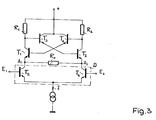
- the circuit arrangement of FIG. 3 differs from the circuit arrangement of FIG. 1 in that the bases of the transistors T1 and T2 are connected via two transistors T3 and T4 working as emitter followers.
- 3 shows, the first emitter follower T3 with the base on the collector of the transistor T1 and with the emitter on the base of the transistor T2, the second emitter follower T4 with the base on the collector of the transistor T2 and with the emitter on the base of transistor T1 connected.
- the collectors of transistors T3 and T4 are connected to the supply voltage.
- the resistors R5 and R6, not shown in FIG. 3, can also be present in the arrangement according to FIG. 2.
- the resting potential of the collectors of the transistors T1 and T2 is higher by the base-emitter voltage of the transistors T3 and T4, and accordingly larger modulations are possible.
- npn transistors results in favorable electrical and structural conditions for the realization as a monolithically integrated semiconductor block.
- pnp transistors when all voltages and currents are reversed is equally possible.
Landscapes
- Engineering & Computer Science (AREA)
- Power Engineering (AREA)
- Amplifiers (AREA)
Description
- Die Erfindung betrifft eine Schaltungsanordnung, die für den Fall, daß das Produkt aus innerer Verstärkung und Rückkopplungsfaktor kleiner als eins ist, als Verstärker und für den Fall, daß das Produkt aus innerer Verstärkung und Rückkopplungsfaktor größer als eins ist, als Schwellwertschalter wirkt, für eine stromgespeiste Differenzstufe, bei der der erste Ausgang der Differenzstufe mit dem Emitter eines ersten Transistors und der zweite Ausgang mit dem Emitter eines zweiten Transistors verbunden ist und bei dem zwei an die Versorgungsspannung angeschlossene Arbeitswiderstände vorgesehen sind, von denen der erste Arbeitswiderstand an den Kollektor des ersten Transistors und die Basis des zweiten Transistors angeschlossen ist und der zweite Arbeitswiderstand an den Kollektor des zweiten Transistors und die Basis des ersten Transistors angeschlossen ist.
- Eine derartige Anordnung, die jedoch keinen Hinweis auf die alternative Verwendung als Verstärker oder Schwellwertschalter gibt, ist aus der Literaturstelle « IBM Technical Disclosure Bulletin, Vol. 23, N° 1, Juni 1980, Seiten 48 und 49", bekannt.
- Die FR-A-13 19 174 hat einen Verstärker zum Gegenstand, bei dem durch Mitkopplung die Werte der Arbeitswiderstände dynamisch vergrößert werden können, einschließlich unendlich oder negative Werte. Die bekannte Schaltung ist jedoch relativ aufwendig und durch die kapazitive Kopplung auf Wechselgrößen beschränkt. Bei der bekannten Schaltung wirken die Ausgänge der Differenzverstärkerstransistoren auf die Basen von Rückkoppeltransistoren ein, deren Kollektoren über Kreuz die Rückkopplung herstellen.
- Der Erfindung liegt die Aufgabe zugrunde, eine Schaltungsanordnung zur Verwendung als rückgekoppelter Verstärker oder Schwellwertschalter anzugeben, die an einer stromgespeisten Differenzstufe angeschlossen ist, eine vereinfachte Schaltungstechnik und geringe Verlustleistung besitzt und die leicht integrierbar ist. Diese Aufgabe wird bei einer Schaltungsanordnung der eingangs erwähnten Art nach der Erfindung dadurch gelöst, daß ein Widerstand zwischen beide Ausgänge der Differenzstufe geschaltet ist, der beim Verstärker mit sinkendem Widerstandswert zur Erhöhung der Stromverstärkung oder beim Schwellwertschalter zum Einstellen des Abstandes der Umschaltpunkte, bei denen der Strom der Stromquelle von einem der Arbeitswiderstände auf den anderen wechselt, dient.
- Die Schaltungsanordnung nach der Erfindung benötigt im Gegensatz zu einem in der DE-B-19 03 913 dargestellten Vorschlag keinen zusätzlichen Versorgungsstrom.
- Bei der erfindungsgemäßen Schaltung kann jede beliebige Stromverstärkung von 1 bis unendlich eingestellt werden. Zusätzlich kann diese Schaltung die Funktion eines Schwellwertschalters mit beliebiger Hysterese erfüllen. Gegenüber der in der DE-B-20 24 806 dargestellten Schaltung besitz sie den Vorteil, daß nach dem Eintritt in den Übersteuerungszustand der Ausgangsstrom seinen Sättigungswert beibehält und nicht zum anderen Arbeitswiderstand wechselt.
- Gemäß einer Weiterbildung der Erfindung ist die Basis des ersten Transistors über einen Widerstand mit dem Kollektor des zweiten Transistors und die Basis des zweiten Transistors über einen Widerstand mit dem Kollektor des ersten Transistors verbunden. Jeweils zwischen Basis und Emitter des ersten bzw. zweiten Transistors ist ein Widerstand eingefügt.
- Eine andere Weiterbildung der Erfindung besteht darin, daß der Basis des ersten Transistors und der Basis des zweiten Transistors je ein als Emitterfolger arbeitender Transistor vorgeschaltet ist. Dies erfolgt im Normalfall so, daß die Basis des ersten Transistors mit dem Emitter des vierten Transistors und die Basis des zweiten Transistors mit dem Emitter des dritten Transistors mit der Versorgungsspannung verbunden sind und daß die Basis des dritten Transistors mit dem Kollektor des ersten Transistors und die Basis des vierten Transistors mit dem Kollektor des zweiten Transistors verbunden sind.
- Die Erfindung wird im folgenden an einem Ausführungsbeispiel näher erläutert.
- Die Figur 1 zeigt eine Schaltungsanordnung, die als rückgekoppelter Verstärker oder als Schwellwertschalter wirksam ist.
- .Die Figur 2 zeigt eine Schaltungsanordnung gemäß der Figur 1, bei der die kreuzgekoppelten Transistoren Basisvorwiderstände aufweisen.
- Die Figur 3 zeigt eine Schaltungsanordnung gemäß Figur 1, bei der die Basen der kreuzgekoppelten Transistoren über zwei als Emitterfolger arbeitende Transistoren angeschlossen sind.
- Die Figur 1 zeigt einen rückgekoppelten Verstärker, dessen zugehörige Differenzstufe D beispielsweise aus den bipolaren Transistoren T5 und T6 besteht und die von einer Stromquelle I beliebiger Ausführungsform gespeist wird. Je nach der Differenz der Potentiale an den Eingangsklemmen E1 und E2 und damit an den Basen der Transistoren T5 und T6 wird der Strom der Stromquelle I auf die beiden Ausgänge A1 und A2 an den Kollektoren der Transistoren T5 und T6 aufgeteilt. Ohne RO zwischen A1 und A2 würden die beiden Teilströme über die Transistoren T1 und T2 nahezu unverändert in die Arbeitswiderstände R1, R2 fließen, soweit die Basisströme der beiden Transistoren T1 und T2 klein bleiben. Steuert man die Differenzstufe D so, daß der Strom im Ausgang A1 stärker und der im Ausgang A2 schwächer wird, so steigt der Spannungsabfall and R1 und sinkt an R2. Durch die Kreuzkopplung der Transistoren T1, T2 werden aber die Spannungsänderungen über die Basis-Emitterstrecken der Transistoren T1 bzw. T2 vertauscht an die Ausgänge A1 und A2 der Differenzstufe D weitergegeben. Während das Potential am Kollektor von T1 sinkt, steigt es am Emitter von T1 an. Der durch RO fließende Strom addiert sich zum vom Eingangssignal verursachten Strom und führt zur Erhöhung der Stromverstärkung. Ist der Widerstand RO gleich der Summe der Arbeitswiderstände R1 und R2 minus der Kehrwerte der beiden Transistorsteilheiten, so wird die Verstärkung unendlich. Das bedeutet, daß der Strom der Stromquelle I bei einem bestimmten Wert der zwischen den Eingangsklemmen E1 und E2 wirksamen Eingangsspannung sprunghaft von einem der Arbeitswiderstände R1 bzw. R2 auf den anderen wechselt. Weitere Verminderungen des Widerstandes RO führt dazu, daß sich der Punkt des Umschaltens des Stromes für steigende Eingangsspannung von dem für fallende EIngangsspannung unterscheidet. Damit ist der Charakter einer Schwellwertschaltung erreicht. Der Abstand der Umschaltpunkte kann durch Wahl von RO beliebig eingestellt werden.
- In der Schaltung nach Fig. 1 ist das Kollektorpotential der Transistoren T1, T2 etwa gleich dem Basispotential. Damit sind nur kleine Aussteuerungen möglich und die Transistoren können leicht in den Sättigungszustand eintreten. Deshalb ist gemäß der Fig. 2 vorgesehen, den Basen des ersten und zweiten Transistors T1 bzw. T2 Widerstände R3 bzw. R4 vorzuschalten. Der Spannungsabfall über diesen Widerständen sorgt für ein gegenüber der Basis erhöhtes Kollektorpotential. Zwei weitere Widerstände R5 und R6, die jeweils zwischen Basis und Emitter des ersten und zweiten Transistors T1 bzw. T2 geschaltet sind, bilden mit den Widerständen R3 und R4 Spannungsteiler, mit denen die Arbeitspunkte des ersten und zweiten Transistors T1 bzw. T2 optimal festgelegt werden können.
- Die Schaltungsanordnung der Fig. 3 unterscheidet sich von der Schaltungsanordnung der Fig. 1 dadurch, daß die Basen der Transistoren T1 und T2 über zwei als Emitterfolger arbeitende Transistoren T3 und T4 angeschlossen sind. Wie die Fig. 3 zeigt, ist der erste Emitterfolger T3 mit der Basis am Kollektor des Transistors T1 und mit dem Emitter an der Basis des Transistors T2, der zweite Emitterfolger T4 mit der Basis am Kollektor des Transistors T2 und mit dem Emitter an der Basis des Transistors T1 angeschlossen. Die Kollektoren der Transistoren T3 und T4 sind mit der Versorgungsspannung verbunden. Zusätzlich können auch die in Fig. 3 nicht eingezeichneten Widerstände R5 und R6 in der Anordnung nach Fig. 2 vorhanden sein. In dieser Form der Erfindung ist das Ruhepotential der Kollektoren der Transistoren T1 und T2 um die Basis-Emitter-Spannung der Transistoren T3 und T4 höher und es sind dadurch entsprechend größere Aussteuerungen möglich.
- Die ausschließliche Verwendung von npn-Transistoren ergibt günstige elektrische und konstruktive Bedingungen für die Realisierung als monolithisch integrierter Halbleiterblock. Die Verwendung von pnp-Transistoren bei Umkehrung aller Spannungen und Ströme ist ebensogut möglich.
Claims (5)
Applications Claiming Priority (2)
| Application Number | Priority Date | Filing Date | Title |
|---|---|---|---|
| DE3032703 | 1980-08-30 | ||
| DE3032703A DE3032703C2 (de) | 1980-08-30 | 1980-08-30 | Rückgekoppelter Verstärker oder Schwellwertschalter für eine stromgespeiste Differenzstufe |
Publications (3)
| Publication Number | Publication Date |
|---|---|
| EP0046878A2 EP0046878A2 (de) | 1982-03-10 |
| EP0046878A3 EP0046878A3 (en) | 1982-05-19 |
| EP0046878B1 true EP0046878B1 (de) | 1985-05-15 |
Family
ID=6110733
Family Applications (1)
| Application Number | Title | Priority Date | Filing Date |
|---|---|---|---|
| EP81105849A Expired EP0046878B1 (de) | 1980-08-30 | 1981-07-24 | Rückgekoppelter Verstärker oder Schwellwertschalter für eine stromgespeiste Differenzstufe |
Country Status (3)
| Country | Link |
|---|---|
| US (1) | US4418321A (de) |
| EP (1) | EP0046878B1 (de) |
| DE (1) | DE3032703C2 (de) |
Families Citing this family (9)
| Publication number | Priority date | Publication date | Assignee | Title |
|---|---|---|---|---|
| NL8003197A (nl) * | 1980-06-02 | 1982-01-04 | Philips Nv | Geintegreerde versterkerschakeling. |
| NL8500080A (nl) * | 1985-01-15 | 1986-08-01 | Philips Nv | Transconductantieversterker. |
| FR2581809A1 (fr) * | 1985-05-10 | 1986-11-14 | Radiotechnique Compelec | Amplificateur pour hautes frequences |
| FR2592538B1 (fr) * | 1985-12-31 | 1988-02-12 | Radiotechnique Compelec | Etage amplificateur differentiel pour hautes frequences et amplificateur le comportant. |
| GB2211044A (en) * | 1987-10-08 | 1989-06-21 | Plessey Co Plc | Linear differential amplifier |
| US5091701A (en) * | 1990-10-15 | 1992-02-25 | Analog Devices, Inc. | High efficiency cross-coupled folded cascode circuit |
| US5493254A (en) * | 1994-03-31 | 1996-02-20 | National Semiconductor Corporation | Amplifier including circuit for reducing input capacitance |
| RU2402151C1 (ru) * | 2009-05-20 | 2010-10-20 | Государственное образовательное учреждение высшего профессионального образования "Южно-Российский государственный университет экономики и сервиса" (ГОУ ВПО "ЮРГУЭС") | Каскодный дифференциальный усилитель |
| US7911276B1 (en) * | 2009-10-29 | 2011-03-22 | Stmicroelectronics Design And Application Gmbh | Transconductor circuit |
Family Cites Families (5)
| Publication number | Priority date | Publication date | Assignee | Title |
|---|---|---|---|---|
| FR1319174A (fr) * | 1962-04-05 | 1963-02-22 | Rotax Ltd | Amplificateur |
| US3408533A (en) * | 1966-03-21 | 1968-10-29 | Tekronix Inc | Low-loss amplification circuit |
| DE1903913C3 (de) * | 1968-01-29 | 1982-09-16 | Tektronix, Inc., 97077 Beaverton, Oreg. | Breitband-Verstärkerschaltung |
| NL6908784A (de) * | 1969-06-10 | 1970-12-14 | ||
| NL8003197A (nl) * | 1980-06-02 | 1982-01-04 | Philips Nv | Geintegreerde versterkerschakeling. |
-
1980
- 1980-08-30 DE DE3032703A patent/DE3032703C2/de not_active Expired
-
1981
- 1981-07-24 EP EP81105849A patent/EP0046878B1/de not_active Expired
- 1981-08-26 US US06/296,484 patent/US4418321A/en not_active Expired - Lifetime
Also Published As
| Publication number | Publication date |
|---|---|
| EP0046878A2 (de) | 1982-03-10 |
| EP0046878A3 (en) | 1982-05-19 |
| DE3032703A1 (de) | 1982-03-11 |
| DE3032703C2 (de) | 1982-12-30 |
| US4418321A (en) | 1983-11-29 |
Similar Documents
| Publication | Publication Date | Title |
|---|---|---|
| DE2323478A1 (de) | Datenuebertragungsanordnung | |
| DE2207233C3 (de) | Elektronischer Signalverstärker | |
| DE3121314C2 (de) | ||
| DE3032703C2 (de) | Rückgekoppelter Verstärker oder Schwellwertschalter für eine stromgespeiste Differenzstufe | |
| DE2905659C3 (de) | Gegentakt-Verstärkerkreis | |
| DE3027071A1 (de) | Transistorverstaerker mit zwei emittergekoppelten transisorpaaren | |
| DE2416534B2 (de) | Transistorschaltung zum umkehren der stromrichtung in einem verbraucher | |
| DE2061943C3 (de) | Differenzverstärker | |
| DE2409929C3 (de) | Verzerrungsarmer, niederfrequenter Gegentakt-Leistungsverstärker | |
| DE2924171C2 (de) | ||
| DE3202501C2 (de) | ||
| DE3810058A1 (de) | Schmitt-trigger-schaltung | |
| EP0119655B1 (de) | Schaltungsanordnung zur Pegelanpassung | |
| DE69128456T2 (de) | Hysterese schaltung | |
| EP0421016A1 (de) | ECL-TTL-Signalpegelwandler | |
| EP0429717B1 (de) | Transkonduktanzverstärker | |
| DE69410654T2 (de) | Stromquelle | |
| DE2056078C3 (de) | Rückgekoppelter Verriegelungsschalter | |
| EP0029480B1 (de) | Emitterfolger-Logikschaltung | |
| DE2148880C2 (de) | Stromquelle in integrierter Schaltungstechnik | |
| DE1814887C3 (de) | Transistorverstärker | |
| DE69010711T2 (de) | Differenzverstärker. | |
| DE3635878C2 (de) | ||
| DE1638010C3 (de) | Festkörperschaltkreis für Referenzverstärker | |
| DE1774527B2 (de) | Schaltungsanordnung zur Bildung des Betrages einer elektrischen Zeitfunktion |
Legal Events
| Date | Code | Title | Description |
|---|---|---|---|
| PUAI | Public reference made under article 153(3) epc to a published international application that has entered the european phase |
Free format text: ORIGINAL CODE: 0009012 |
|
| AK | Designated contracting states |
Designated state(s): FR GB IT NL |
|
| PUAL | Search report despatched |
Free format text: ORIGINAL CODE: 0009013 |
|
| AK | Designated contracting states |
Designated state(s): FR GB IT NL |
|
| 17P | Request for examination filed |
Effective date: 19820622 |
|
| RAP1 | Party data changed (applicant data changed or rights of an application transferred) |
Owner name: TELEFUNKEN ELECTRONIC GMBH |
|
| ITF | It: translation for a ep patent filed | ||
| GRAA | (expected) grant |
Free format text: ORIGINAL CODE: 0009210 |
|
| AK | Designated contracting states |
Designated state(s): FR GB IT NL |
|
| ET | Fr: translation filed | ||
| PLBE | No opposition filed within time limit |
Free format text: ORIGINAL CODE: 0009261 |
|
| STAA | Information on the status of an ep patent application or granted ep patent |
Free format text: STATUS: NO OPPOSITION FILED WITHIN TIME LIMIT |
|
| 26N | No opposition filed | ||
| PGFP | Annual fee paid to national office [announced via postgrant information from national office to epo] |
Ref country code: NL Payment date: 19870731 Year of fee payment: 7 |
|
| PG25 | Lapsed in a contracting state [announced via postgrant information from national office to epo] |
Ref country code: GB Effective date: 19880724 |
|
| PG25 | Lapsed in a contracting state [announced via postgrant information from national office to epo] |
Ref country code: NL Effective date: 19890201 |
|
| NLV4 | Nl: lapsed or anulled due to non-payment of the annual fee | ||
| GBPC | Gb: european patent ceased through non-payment of renewal fee | ||
| ITTA | It: last paid annual fee | ||
| PGFP | Annual fee paid to national office [announced via postgrant information from national office to epo] |
Ref country code: FR Payment date: 19940705 Year of fee payment: 14 |
|
| PG25 | Lapsed in a contracting state [announced via postgrant information from national office to epo] |
Ref country code: FR Effective date: 19960430 |
|
| REG | Reference to a national code |
Ref country code: FR Ref legal event code: ST |
|
| REG | Reference to a national code |
Ref country code: FR Ref legal event code: ST |
|
| REG | Reference to a national code |
Ref country code: FR Ref legal event code: ST |