EP0044571A2 - Halbleiterlaservorrichtung - Google Patents
Halbleiterlaservorrichtung Download PDFInfo
- Publication number
- EP0044571A2 EP0044571A2 EP81105841A EP81105841A EP0044571A2 EP 0044571 A2 EP0044571 A2 EP 0044571A2 EP 81105841 A EP81105841 A EP 81105841A EP 81105841 A EP81105841 A EP 81105841A EP 0044571 A2 EP0044571 A2 EP 0044571A2
- Authority
- EP
- European Patent Office
- Prior art keywords
- semiconductor
- layer
- layers
- semiconductor layer
- active layer
- Prior art date
- Legal status (The legal status is an assumption and is not a legal conclusion. Google has not performed a legal analysis and makes no representation as to the accuracy of the status listed.)
- Granted
Links
Images

Classifications
-
- H—ELECTRICITY
- H01—ELECTRIC ELEMENTS
- H01S—DEVICES USING THE PROCESS OF LIGHT AMPLIFICATION BY STIMULATED EMISSION OF RADIATION [LASER] TO AMPLIFY OR GENERATE LIGHT; DEVICES USING STIMULATED EMISSION OF ELECTROMAGNETIC RADIATION IN WAVE RANGES OTHER THAN OPTICAL
- H01S5/00—Semiconductor lasers
- H01S5/20—Structure or shape of the semiconductor body to guide the optical wave ; Confining structures perpendicular to the optical axis, e.g. index or gain guiding, stripe geometry, broad area lasers, gain tailoring, transverse or lateral reflectors, special cladding structures, MQW barrier reflection layers
- H01S5/22—Structure or shape of the semiconductor body to guide the optical wave ; Confining structures perpendicular to the optical axis, e.g. index or gain guiding, stripe geometry, broad area lasers, gain tailoring, transverse or lateral reflectors, special cladding structures, MQW barrier reflection layers having a ridge or stripe structure
- H01S5/227—Buried mesa structure ; Striped active layer
- H01S5/2275—Buried mesa structure ; Striped active layer mesa created by etching
Definitions
- This invention relates to buried-heterostructure lasers with a buried optical guide which produce high outputs and which facilitate stable oscillations in fundamental modes.
- an optical guide layer is introduced in adjacency to an active layer in a double-heterostructure.
- a semiconductor laser of a GaAs-GaAlAs heterostructure wherein one layer of GaAs is interposed between two layers of GaAlAs, the GaAs layer forms the P M-junction of the laser, at least one of the GaAlAs layers is an inner layer, and the inner layer is overlaid with an outer layer of GaAlAs having a greater mole fraction of AlAs than the inner layer.
- Examples of this type of semiconductor laser are disclosed in the official gazette of Japanese Laid-open Patent Application No. 47-8472; 'Appl. phys. Lett.', 35 (7), 1 October 1979, pp. 513-516; etc.
- the semiconductor laser of this type ha& a structure in which photons and carriers are confined between different semiconductor layers.
- This invention intends to provide an element structure with which high-output semiconductor laser elements of the specified type can be produced at very high yield.
- This invention consists in a structure in which the central part of an optical resonator of a semiconductor laser with an optical guide is preponderantly excited, whereas both the end parts are not excited.
- the fundamental structure is as follows.
- At least first, second, third and fourth semiconductor layers are stacked on a predetermined semiconductor body.
- the second semiconductor layer is set to be low in the refractive index relatively to the third semiconductor layer
- the first and fourth semiconductor layers are set to be low in the refractive index relatively to both the second and third semiconductor layers and also to have conductivity types opposite to each other
- the fourth and second semiconductor layers are set to be wide in the band gap relatively to the third semiconductor layer.
- a semiconductor material assembly including the first, second, third and fourth semiconductor layers has its side surfaces, parallel to the travelling direction of a laser beam, buried in a fifth semiconductor layer.
- the refractive index of the fifth semiconductor layer is at least lower than that of the third semiconductor layer
- the band gap of the fifth semiconductor layer is at least wider than that of the third semiconductor layer.
- the width of the mesa changes in the stacked direction of the layers, and the narrowest part of the mesa is located on the side opposite to the second semiconductor layer with reference to the position of the third semiconductor layer.
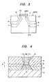
- Figure 1 is a perspective view of a typical semiconductor laser device according to this invention.
- n-Ga 1-x Al x As (0.2 ⁇ ⁇ ⁇ 0.6) layer 1 On a GaAs substrate 10 having the (100) face as its upper surface, there are formed an n-Ga 1-x Al x As (0.2 ⁇ ⁇ ⁇ 0.6) layer 1, an n-Ga 1-z Al z As (0.1 ⁇ z ⁇ 0.5) layer 2, a Ga 1-w Al w As (0 ⁇ w ⁇ 0.3) layer 3 and a p-Ga 1-v Al v As (0.2 ⁇ v ⁇ 0.6) layer 4.
- a semiconductor layer 6 is a burying'layer which is a Ga 1-u Al u As (0.1 ⁇ u ⁇ 0.6) layer.
- the burying layer is preferably made a high-resistivity semiconductor layer having a resistivity of at least approximately 10 4 ⁇ cm, or a construction which consists of a plurality of layers and in which a p-n junction is formed and is reverse-biased during the operation of the laser.
- the position of the active layer 3 lies below the position 14 of the constriction of the mesa-shaped semiconductor layers. That is, the narrowest part of the mesa lies on the side opposite to the optical guide layer with reference to the position of the active layer.
- the width of, the active layer 3 can be made smaller than that of the optical guide layer 2 in which a laser beam can exist. Accordingly, the laser beam is distributed in the central part of the active layer 3 as well as the optical guide layer 2. Since, however, a gain is attained in the active layer region, only a middle part is excited in the section of a waveguide portion.
- the equivalent refractive index in the lateral direction varies gradually, with the result that higher-order modes become difficult of excitation. In this way, it becomes easy to attain stable oscillations in the fundamental mode.
- the optical resonator is excited up to its end parts and the higher-order modes become easy of generation.
- numerals 11 and 13 indicate electrodes.
- the electrode 11 is made of Au + AuGeNi
- the electrode 13 is made of Cr + Au.
- the active layer 3 and the cladding layers 1 and 4 may be constructed as in the prior-art double-heterostructure.
- the thickness of the active layer 3 is selected in a range of 0.02 ⁇ m to 0.2 ⁇ m
- the thicknesses of the cladding layers 1 and 4 are selected in a range of 0.3 ⁇ m to 2.5 ⁇ m or so.
- the thicknesses of the cladding layers 1 and 4 do not affect characteristics so greatly as the thicknesses of the active layer and the optical guide layer to be described later.
- the respective refractive indices n 3 and n 1 of the active layer 3 and the first cladding layer 1 are set in practical use so that their difference may be 0.18 - 0.22 or so.
- the first and second cladding layers 1 and 4 have conductivity types opposite to each other.
- the semiconductor body 10 is sometimes made up of a plurality of semiconductor layers.
- a semiconductor layer is further disposed on the second cladding layer 4 as, for example, a cap layer.
- the basic structure is as stated above.
- the optical guide layer is introduced which differs in the band gap from the active layer at least 0.15 eV. Owing to this expedient, it is possible to maintain the temperature characteristic of a treshold current density very stable and to increase the optical output.
- the refractive index profile of the stacked structure of the foregoing example is as shown in Figure 2.
- the refractive index n 3 of the active layer 3 and the refractive indices n 1 and n 4 of the respective cladding layers 1 and 4 are brought into the relationship of n 3 > n 1 , n 4 , which is the same as in the prior-art double-heterostructure.
- the refractive index n 2 of the optical guide layer 2 is set at n 3 > n 2 > n 1 , n 4 . Owing to this relationship of the refractive indices, the laser beam becomes distributed in the active layer and the optical guide layer, and an increase of the optical output can be achieved.
- the respective band gaps E g3 , E g1 and E g2 of the active layer 3, the adjoining cladding layer 1 and the optical guide layer 2 are brought into the relationship of E g3 ⁇ E g1 , E g2 , whereby the confinement of carriers into the active layer is made sufficient.
- the difference between the band gaps of the optical guide layer 2 and the active layer 3 needs to be at least 0.15 eV.
- an n-type Ga 1-x Al x As (0.2 ⁇ x ⁇ 0.6) layer 1 (doped with Sn, carrier concentration of 5 ⁇ 10 17 cm -3 )
- an n-type Ga 1-y Al y As (0.1 ⁇ y ⁇ 0.3) layer 2 (doped with Sn, carrier concentration of 5 x 10 17 cm -3 )
- a Ga 1-w Al w As (0 ⁇ w ⁇ 0.15) layer 3 undoped, carrier concentration of 1 x 10 17 cm -3
- a p-type Ga 1-v Al v As (0.2 ⁇ v ⁇ 0.4) layer 4 (doped with Ge, carrier concentration of 1 x 10 18 cm -3 ) are continuously grown by the well-known liquid phase epitaxy.
- a striped mask having a strip width of approximately 10 f m is formed on the surface of the semiconductor layer 4.
- a PSG film is first deposited on the crystal surface to a thickness of approximately 400 nm, and parts other than the strip are removed by the well-known etching process employing a photoresist.
- the direction of the striped mask is made the ⁇ 011> orientation.
- an etchant for example, a mixed solution consisting of H 3 PO 4 : 1 - H 2 O 2 : 1 - CH 3 OH : 3
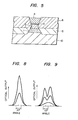
- Numeral 21 denotes the semiconductor crystal of the stacked layers, and numeral 20 the etching mask.
- the (221) and (111) faces often appear in case of the GaAs-GaAlAs system semiconductor crystal.
- An angle of about 71 0 is defined between the (100) face and the (221) face, and an angle of about 54.° between the (100) face and the (111) face.
- the position of the wedge of the mesa-shaped semiconductor layers can be determined.
- the etching condition is 8 minutes at 20 °C.
- the strip width is usually set at a range of at most 3.2 ⁇ m. In practical use, the lower limit of the strip width is approximately 0.5 ⁇ m for reasons of fabrication.
- a Ga 1-u Al u As layer 6 is grown on the mesa-shaped semiconductor layers other than the strip portion by the well-known liquid phase epitaxy.
- u > w is set in order to confine the light distribution to the strip portion.
- a p-type Ga 1-u Al u As layer (doped with Ge, p ⁇ 1 x 10 17 cm- 3 ) and an n-type Ga 1-u Al u As layer (doped with Ge, n ⁇ 5 ⁇ 10 13 cm -3 ) are successively grown into a double-layer structure. This is intended to block current owing to the reverse bias of the p-n junction and to cause current to flow through the strip portion efficiently. Of course, a construction including more layers is allowed.
- Ga 1-u Al u As layer of high resistivity > 10 4 ⁇ cm
- the Ga 1-u Al u As layer of high resistivity was formed in such a way that an undoped Ga-Al-As ternary solution was baked in E 2 at 800 - 900 °C for about 5 hours and was thereafter started to grow. Also in this case, a structure adapted to efficiently inject the current to the stripe portion could be formed.
- an Si0 2 film 12 is formed to a thickness of 300 nm by the CVD process.
- a region which corresponds to the upper part of the stacked structure of the semiconductor layers is selectively removed in the shape of a 3 ⁇ m wide stripe.
- Cr + Au is deposited by evaporation as a p-side electrode 13
- Au + AuGeNi is an n-side electrode 11.
- Figure 4 is a sectional view of the semiconductor laser of the present embodiment as taken along a plane parallel to optically flat faces constituting a Fabry-Perot resonator.
- Figure 5 is a similar sectional view concerning an example in which the active layer lies above the position of the constriction of the mesa-shaped semiconductor layers. Numerals in the respective figures indicate the same parts as in the previous description.
- the transverse mode of a semiconductor laser is closely related with the width (W a ) of the active layer and the position ( ⁇ ) of the active layer (as well as the optical guide layer) with respect to the constriction.
- W a and d The way of taking W a and d is illustrated in Figure 4.
- ⁇ is denoted as plus in case where the active layer lies above the constriction, and as minus in case where it lies below the constriction.
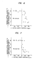
- Figures 6 and 7 illustrate the relationships between the position ( ⁇ ; ⁇ m) of the active layer and the maximum possible optical output (mW) in the transverse fundamental.
- Figure 6 shows the results of samples in which the strip widths (W a ) were 1.8 ⁇ m- 2.3 um and comparatively small
- Figure 7 shows the results of samples in which they were 2.8 ⁇ m - 3.3 ⁇ m and comparatively great.
- the samples whose dots are assigned arrows exhibited at least the indicated values. It is understood from the results of both graphs that, by locating the position of the active layer below the constriction, the maximum optical output in the transverse fundamental mode can be made much higher than in case of locating the position of the active layer above the constriction.
- the interpretation is possible that the range permitting a stable operation has been allowed to further expand the strip width (W a ) to approximately 3.0 ⁇ m - 3.3 ⁇ m.
- Figures 8 and 9 show examples of far-field patterns in the case where the position of the active layer lies below the constriction, i. e., where the structure of Figure 4 is employed, and the case where the position of the active layer lies above the constriction, i. e., where the structure of Figure 5 is employed, respectively.
- the axes of abscissas indicate the horizontal direction.
- the example of Figure 8 can hold the transverse fundamental mode even when the optical output is increased, whereas the example of Figure 9 falls into multi-mode oscillations ' due to an increase of the optical output.
- the semiconductor material assembly for the optical confinement is formed on the n-type semiconductor substrate, it is also possible to form a semiconductor material assembly on a p-type semiconductor substrate.
- an optical guide layer is advantageously inserted between an n-type cladding layer and an active layer. The reason therefor is that positive holes are blocked at the interface between the active layer and the n-type cladding layer, while electrons are blocked at the interface of a p-type cladding layer, and that the p-type cladding layer side is susceptible to thermal influences on the leakage current.
- the optical guide layer is interposed between the active layer and the n-type cladding layer, and on the p-side, the p-type cladding layer is utilized to secure a great band gap difference from the active layer.
- the active layer and the overlying optical guide layer come to lie above the narrowest part of the mesa.
- this invention is extensively applicable to an InP-InGaAsP system, InGap-GaAlAs system, GaAlSb-GaAlSbAs system etc. besides the GaAs-GaAlAs system.
Landscapes
- Physics & Mathematics (AREA)
- Geometry (AREA)
- Condensed Matter Physics & Semiconductors (AREA)
- General Physics & Mathematics (AREA)
- Electromagnetism (AREA)
- Optics & Photonics (AREA)
- Semiconductor Lasers (AREA)
Applications Claiming Priority (2)
| Application Number | Priority Date | Filing Date | Title |
|---|---|---|---|
| JP9991880A JPS5726487A (en) | 1980-07-23 | 1980-07-23 | Semiconductor laser device |
| JP99918/80 | 1980-07-23 |
Publications (3)
| Publication Number | Publication Date |
|---|---|
| EP0044571A2 true EP0044571A2 (de) | 1982-01-27 |
| EP0044571A3 EP0044571A3 (en) | 1983-01-05 |
| EP0044571B1 EP0044571B1 (de) | 1986-04-09 |
Family
ID=14260153
Family Applications (1)
| Application Number | Title | Priority Date | Filing Date |
|---|---|---|---|
| EP81105841A Expired EP0044571B1 (de) | 1980-07-23 | 1981-07-23 | Halbleiterlaservorrichtung |
Country Status (5)
| Country | Link |
|---|---|
| US (1) | US4426702A (de) |
| EP (1) | EP0044571B1 (de) |
| JP (1) | JPS5726487A (de) |
| CA (1) | CA1150810A (de) |
| DE (1) | DE3174308D1 (de) |
Cited By (12)
| Publication number | Priority date | Publication date | Assignee | Title |
|---|---|---|---|---|
| EP0076761A1 (de) * | 1981-10-05 | 1983-04-13 | Fujitsu Limited | Halbleiterlaser und Verfahren zu ihrer Herstellung |
| DE3502326A1 (de) * | 1984-01-25 | 1985-08-01 | Hitachi, Ltd., Tokio/Tokyo | Licht emittierender chip und damit arbeitende optische kommunikationsvorrichtung |
| GB2154059A (en) * | 1984-01-25 | 1985-08-29 | Hitachi Ltd | Light emitting chip and communication apparatus using the same |
| EP0272096A2 (de) * | 1986-12-15 | 1988-06-22 | Sharp Kabushiki Kaisha | Halbleiterlaser |
| US4860299A (en) * | 1987-05-19 | 1989-08-22 | Sharp Kabushiki Kaisha | Semiconductor laser device |
| US4862470A (en) * | 1987-04-28 | 1989-08-29 | Sharp Kabushiki Kaisha | Semiconductor laser device |
| US4862472A (en) * | 1987-01-16 | 1989-08-29 | Sharp Kabushiki Kaisha | Semiconductor laser device |
| US4868838A (en) * | 1986-07-10 | 1989-09-19 | Sharp Kabushiki Kaisha | Semiconductor laser device |
| US4887274A (en) * | 1986-12-15 | 1989-12-12 | Sharp Kabushiki Kaisha | Deterioration-resistant superlattice semiconductor laser device |
| US4894836A (en) * | 1987-02-24 | 1990-01-16 | Sharp Kabushiki Kaisha | Semiconductor device |
| EP0590951A2 (de) * | 1992-09-29 | 1994-04-06 | Mitsubishi Chemical Corporation | Halbleiterlaser |
| DE19520739A1 (de) * | 1994-06-07 | 1995-12-14 | Mitsubishi Electric Corp | Lichtemittierende Halbleitervorrichtung, Laser-Resonanzverstärker und Lichtverstärker mit integriertem Wellenlängen-abstimmbaren Filter |
Families Citing this family (11)
| Publication number | Priority date | Publication date | Assignee | Title |
|---|---|---|---|---|
| US4536940A (en) * | 1981-06-12 | 1985-08-27 | At&T Bell Laboratories | Method of making a loss stabilized buried heterostructure laser |
| GB2115608B (en) * | 1982-02-24 | 1985-10-30 | Plessey Co Plc | Semi-conductor lasers |
| US4566171A (en) * | 1983-06-20 | 1986-01-28 | At&T Bell Laboratories | Elimination of mask undercutting in the fabrication of InP/InGaAsP BH devices |
| US4661961A (en) * | 1983-06-20 | 1987-04-28 | American Telephone And Telegraph Company, At&T Bell Laboratories | Buried heterostructure devices with unique contact-facilitating layers |
| JPS6085585A (ja) * | 1983-10-17 | 1985-05-15 | Nec Corp | 埋め込み型半導体レ−ザ |
| JPS6197189A (ja) * | 1984-10-16 | 1986-05-15 | Matsushita Electric Ind Co Ltd | 液相成長方法 |
| US4652333A (en) * | 1985-06-19 | 1987-03-24 | Honeywell Inc. | Etch process monitors for buried heterostructures |
| US4818722A (en) * | 1986-09-29 | 1989-04-04 | Siemens Aktiengesellschaft | Method for generating a strip waveguide |
| US4972238A (en) * | 1987-12-08 | 1990-11-20 | Kabushiki Kaisha Toshiba | Semiconductor laser device |
| DE3856396T2 (de) * | 1988-01-06 | 2000-08-31 | Telstra Corp Ltd | Strominjektionslaser |
| JP2763008B2 (ja) * | 1988-11-28 | 1998-06-11 | 三菱化学株式会社 | ダブルヘテロ型エピタキシャル・ウエハおよび発光ダイオード |
-
1980
- 1980-07-23 JP JP9991880A patent/JPS5726487A/ja active Granted
-
1981
- 1981-07-15 US US06/283,791 patent/US4426702A/en not_active Expired - Lifetime
- 1981-07-16 CA CA000381881A patent/CA1150810A/en not_active Expired
- 1981-07-23 DE DE8181105841T patent/DE3174308D1/de not_active Expired
- 1981-07-23 EP EP81105841A patent/EP0044571B1/de not_active Expired
Non-Patent Citations (4)
| Title |
|---|
| APPLIED PHYSICS LETTERS, vol. 35, no. 7, October 1979, pages 513-516, New York (USA); * |
| APPLIED PHYSICS LETTERS, vol. 36, no. 9, May 1980, pages 730-732, New York (USA); * |
| APPLIED PHYSICS LETTERS, vol. 36, no. 9, May 1980, pages 730-732, New York (USA); W.T.TSANG et al.: "GaAs-AlxGal-x As buried-heterostructure lasers grown by molecular beam epitaxy with A10.65GaO.35As (Ge-doped) liquid phase epitaxy overgrown layer for current injection confinement" * |
| JAPANESE JOURNAL OF APPLIED PHYSICS, vol. 19, no. 10, October 1980, pages L591-4, Tokyo (JP); * |
Cited By (19)
| Publication number | Priority date | Publication date | Assignee | Title |
|---|---|---|---|---|
| EP0076761A1 (de) * | 1981-10-05 | 1983-04-13 | Fujitsu Limited | Halbleiterlaser und Verfahren zu ihrer Herstellung |
| DE3502326A1 (de) * | 1984-01-25 | 1985-08-01 | Hitachi, Ltd., Tokio/Tokyo | Licht emittierender chip und damit arbeitende optische kommunikationsvorrichtung |
| GB2154059A (en) * | 1984-01-25 | 1985-08-29 | Hitachi Ltd | Light emitting chip and communication apparatus using the same |
| US4701927A (en) * | 1984-01-25 | 1987-10-20 | Hitachi, Ltd. | Light emitting chip and optical communication apparatus using the same |
| US4868838A (en) * | 1986-07-10 | 1989-09-19 | Sharp Kabushiki Kaisha | Semiconductor laser device |
| US4887274A (en) * | 1986-12-15 | 1989-12-12 | Sharp Kabushiki Kaisha | Deterioration-resistant superlattice semiconductor laser device |
| EP0272096A2 (de) * | 1986-12-15 | 1988-06-22 | Sharp Kabushiki Kaisha | Halbleiterlaser |
| EP0272096A3 (en) * | 1986-12-15 | 1989-01-25 | Sharp Kabushiki Kaisha | A semiconductor laser device |
| US4852111A (en) * | 1986-12-15 | 1989-07-25 | 501 Sharp Kabushiki Kaisha | Semiconductor laser device |
| US4907239A (en) * | 1986-12-15 | 1990-03-06 | Sharp Kabushiki Kaisha | Semiconductor laser device |
| US4862472A (en) * | 1987-01-16 | 1989-08-29 | Sharp Kabushiki Kaisha | Semiconductor laser device |
| US4894836A (en) * | 1987-02-24 | 1990-01-16 | Sharp Kabushiki Kaisha | Semiconductor device |
| US4862470A (en) * | 1987-04-28 | 1989-08-29 | Sharp Kabushiki Kaisha | Semiconductor laser device |
| US4860299A (en) * | 1987-05-19 | 1989-08-22 | Sharp Kabushiki Kaisha | Semiconductor laser device |
| EP0590951A2 (de) * | 1992-09-29 | 1994-04-06 | Mitsubishi Chemical Corporation | Halbleiterlaser |
| EP0590951A3 (de) * | 1992-09-29 | 1994-04-13 | Mitsubishi Chemical Corporation | Halbleiterlaser |
| US5355384A (en) * | 1992-09-29 | 1994-10-11 | Mitsubishi Kasei Corporation | Semiconductor laser element |
| DE19520739A1 (de) * | 1994-06-07 | 1995-12-14 | Mitsubishi Electric Corp | Lichtemittierende Halbleitervorrichtung, Laser-Resonanzverstärker und Lichtverstärker mit integriertem Wellenlängen-abstimmbaren Filter |
| US5661741A (en) * | 1994-06-07 | 1997-08-26 | Mitsubishi Denki Kabushiki Kaisha | Semiconductor light emitting device, laser amplifier, and integrated light amplifier and wavelength variable filter |
Also Published As
| Publication number | Publication date |
|---|---|
| EP0044571A3 (en) | 1983-01-05 |
| JPS5726487A (en) | 1982-02-12 |
| EP0044571B1 (de) | 1986-04-09 |
| CA1150810A (en) | 1983-07-26 |
| JPS6124838B2 (de) | 1986-06-12 |
| DE3174308D1 (en) | 1986-05-15 |
| US4426702A (en) | 1984-01-17 |
Similar Documents
| Publication | Publication Date | Title |
|---|---|---|
| US4426702A (en) | Semiconductor laser device | |
| US4503540A (en) | Phase-locked semiconductor laser device | |
| EP0029167B1 (de) | Halbleiter-Laservorrichtung | |
| EP0064339B1 (de) | Halbleiterlaservorrichtung | |
| EP0590951B1 (de) | Halbleiterlaser-Element | |
| EP0095826A2 (de) | Halbleiterlaser | |
| US4948753A (en) | Method of producing stripe-structure semiconductor laser | |
| EP0264225B1 (de) | Halbleiterlaservorrichtung und Verfahren zur Herstellung derselben | |
| US4602371A (en) | High output semiconductor laser device utilizing a mesa-stripe optical confinement region | |
| JPH06302908A (ja) | 半導体レーザ | |
| JPH0461514B2 (de) | ||
| EP0085423B1 (de) | Halbleiterlaservorrichtung | |
| US4752933A (en) | Semiconductor laser | |
| EP0076761B1 (de) | Halbleiterlaser und Verfahren zu ihrer Herstellung | |
| EP0298778B1 (de) | Halbleiterlaservorrichtungen und Verfahren zur Herstellung derselben | |
| US5490159A (en) | Visible light semiconductor laser | |
| US20040119080A1 (en) | Semiconductor optical device | |
| US4860299A (en) | Semiconductor laser device | |
| JPH06283801A (ja) | 半導体レーザ | |
| JPS6212678B2 (de) | ||
| JP4024319B2 (ja) | 半導体発光装置 | |
| EP0118671A1 (de) | Halbleiterlaservorrichtung | |
| JP2814124B2 (ja) | 埋込み形半導体発光素子 | |
| JPS61137386A (ja) | 二重ヘテロ構造半導体レ−ザ | |
| Okajima et al. | Transverse-mode stabilized GaAlAs laser with an embedded confining layer on optical guide by MOCVD |
Legal Events
| Date | Code | Title | Description |
|---|---|---|---|
| PUAI | Public reference made under article 153(3) epc to a published international application that has entered the european phase |
Free format text: ORIGINAL CODE: 0009012 |
|
| 17P | Request for examination filed |
Effective date: 19811015 |
|
| AK | Designated contracting states |
Designated state(s): DE FR GB NL |
|
| PUAL | Search report despatched |
Free format text: ORIGINAL CODE: 0009013 |
|
| AK | Designated contracting states |
Designated state(s): DE FR GB NL |
|
| GRAA | (expected) grant |
Free format text: ORIGINAL CODE: 0009210 |
|
| AK | Designated contracting states |
Kind code of ref document: B1 Designated state(s): DE FR GB NL |
|
| REF | Corresponds to: |
Ref document number: 3174308 Country of ref document: DE Date of ref document: 19860515 |
|
| ET | Fr: translation filed | ||
| PLBE | No opposition filed within time limit |
Free format text: ORIGINAL CODE: 0009261 |
|
| STAA | Information on the status of an ep patent application or granted ep patent |
Free format text: STATUS: NO OPPOSITION FILED WITHIN TIME LIMIT |
|
| 26N | No opposition filed | ||
| PGFP | Annual fee paid to national office [announced via postgrant information from national office to epo] |
Ref country code: FR Payment date: 19980710 Year of fee payment: 18 |
|
| PGFP | Annual fee paid to national office [announced via postgrant information from national office to epo] |
Ref country code: NL Payment date: 19980731 Year of fee payment: 18 |
|
| PGFP | Annual fee paid to national office [announced via postgrant information from national office to epo] |
Ref country code: DE Payment date: 19980928 Year of fee payment: 18 |
|
| PGFP | Annual fee paid to national office [announced via postgrant information from national office to epo] |
Ref country code: GB Payment date: 19990625 Year of fee payment: 19 |
|
| PG25 | Lapsed in a contracting state [announced via postgrant information from national office to epo] |
Ref country code: FR Free format text: THE PATENT HAS BEEN ANNULLED BY A DECISION OF A NATIONAL AUTHORITY Effective date: 19990731 |
|
| PG25 | Lapsed in a contracting state [announced via postgrant information from national office to epo] |
Ref country code: NL Free format text: LAPSE BECAUSE OF NON-PAYMENT OF DUE FEES Effective date: 20000201 |
|
| NLV4 | Nl: lapsed or anulled due to non-payment of the annual fee |
Effective date: 20000201 |
|
| PG25 | Lapsed in a contracting state [announced via postgrant information from national office to epo] |
Ref country code: DE Free format text: LAPSE BECAUSE OF NON-PAYMENT OF DUE FEES Effective date: 20000503 |
|
| REG | Reference to a national code |
Ref country code: FR Ref legal event code: ST |
|
| PG25 | Lapsed in a contracting state [announced via postgrant information from national office to epo] |
Ref country code: GB Free format text: LAPSE BECAUSE OF NON-PAYMENT OF DUE FEES Effective date: 20000723 |
|
| GBPC | Gb: european patent ceased through non-payment of renewal fee |
Effective date: 20000723 |