EP0037663B1 - Method and apparatus for positioning a wafer on a flat bed - Google Patents
Method and apparatus for positioning a wafer on a flat bed Download PDFInfo
- Publication number
- EP0037663B1 EP0037663B1 EP19810301198 EP81301198A EP0037663B1 EP 0037663 B1 EP0037663 B1 EP 0037663B1 EP 19810301198 EP19810301198 EP 19810301198 EP 81301198 A EP81301198 A EP 81301198A EP 0037663 B1 EP0037663 B1 EP 0037663B1
- Authority
- EP
- European Patent Office
- Prior art keywords
- wafer
- distinctiveness
- reference portion
- image structure
- flat bed
- Prior art date
- Legal status (The legal status is an assumption and is not a legal conclusion. Google has not performed a legal analysis and makes no representation as to the accuracy of the status listed.)
- Expired
Links
Images


Classifications
-
- G—PHYSICS
- G03—PHOTOGRAPHY; CINEMATOGRAPHY; ANALOGOUS TECHNIQUES USING WAVES OTHER THAN OPTICAL WAVES; ELECTROGRAPHY; HOLOGRAPHY
- G03F—PHOTOMECHANICAL PRODUCTION OF TEXTURED OR PATTERNED SURFACES, e.g. FOR PRINTING, FOR PROCESSING OF SEMICONDUCTOR DEVICES; MATERIALS THEREFOR; ORIGINALS THEREFOR; APPARATUS SPECIALLY ADAPTED THEREFOR
- G03F7/00—Photomechanical, e.g. photolithographic, production of textured or patterned surfaces, e.g. printing surfaces; Materials therefor, e.g. comprising photoresists; Apparatus specially adapted therefor
- G03F7/70—Microphotolithographic exposure; Apparatus therefor
- G03F7/70691—Handling of masks or workpieces
- G03F7/70716—Stages
Definitions
- This invention relates to methods of, and apparatus for, performing precision operations on the dies of semiconductor wafers. More particularly, the invention relates to methods of, and apparatus for, providing such operations with greater precision and reliability than in the prior art.
- the semiconductors are formed on wafers, each of which contains a plurality of dies with electrical circuitry printed on the dies.
- wafers each of which contains a plurality of dies with electrical circuitry printed on the dies.
- electrical circuitry printed on the dies.
- a considerable effort has been made to keep pace with the advances in the semiconductor technology in the methods of, and apparatus for, testing semiconductors on the dies of each wafer.
- such efforts have not been entirely successful.
- U.S. Patents Numbers 3,899,634 and 4,163,212 as well as French Patent 2,219,398 exemplify the state of the art in this respect.
- United States Patent 3,899,634 senses a coincidence of a video signal of an article and a video signal of a boundary marker to move the article until the video signal of the article and the video signal of the boundary marker do not coincide.
- a pair of coordinate axes such as X and Y axes
- U.S. Patent4,163,212 scans a "blob" in at least two perpendicular directions to locate the center of the block. Scanning in two coordinate directions is sometimes not enough depending upon the characteristics of the blob. It is then necessary to scan in two other directions which are coordinate with each other and which are transverse relative to the first pair of coordinate directions. A blob does not constitute the best material to be scanned.
- a blob certainly does not provide the distinctiveness obtained by the present invention in the distinctive portion.
- a method of positioning each wafer of a plurality of wafers, using a flat bed for supporting the wafer to perform precision operations on the wafer thereafter where each of the wafers in the plurality has a plurality of printed dies disposed in at least one row and each die in the at least one row has a corresponding image characterized by the following steps:
- the invention preferably uses video techniques to obtain such advanced methods and apparatus.
- video techniques provide for the selection of a distinctive area as a preselected reference area and for the use of this reference area in progressively positioning the individual dies on each wafer precisely to test the electrical circuitry on the individual dies on the wafer.
- a distinctive portion of a first wafer is chosen.
- the distinctiveness of the portion is verified by visually comparing the distinctive portion to portions intermediate to the distinctive portion and disposed around the distinctive portion.
- the distinctive portion is then compared with progressive portions on the wafer along a particular axis to determine rotary deviations of the wafer from disposition along the particular axis. Corrections are then made in the rotary disposition of the wafer in accordance with such comparisons. The displacement of such distinctive portion from a starting position on the wafer is then determined.
- Each progressive wafer in the plurality is then sequentially selected for the precision operation.
- the distinctive portion on each wafer is initially selected and is subsequently confirmed by comparing the distinctive portion with the intermediate portions around the distinctive portion.
- the distinctive portion is then compared with progressive portions on the wafer along the particular axis to determine any rotary deviations of the wafer from disposition along the particular axis. Corrections are then made in the rotary deviation of each progressive wafer from disposition along the particular axis.
- Each progressive wafer is then displaced to the starting position.
- the precision operation is thereafter performed sequentially on the different dies on each progressive wafer and the wafer is advanced to the next one of the progressive dies upon each such completion of such precision operation.
- Such precision operation may constitute the testing of electrical circuitry on the dies to determine if such circuitry has preselected characteristics.
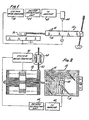
- apparatus for performing precision operations on a plurality of dies 10 which are disposed in rows and columns on a wafer generally indicated at 12.
- the precision operation may involve the testing of the electrical circuitry on each of the dies to determine if the electrical circuitry has been constructed properly.
- the embodiment of this invention includes a flat bed 14 for receiving sequentially each of the progressive wafers 12 in the plurality.
- a precision motor generally indicated at 16 is operatively coupled to the flat bed 14 for driving the flat bed 14 in first and second coordinate directions such as along the X and Y axes.
- the motor 16 may be constructed in a manner similar to that disclosed and claimed in United States Patent No. 3,851,196 issued to Walter E. Hinds on November 26,1974, and assigned of record to General Signal Corporation.
- the embodiment of this invention further includes a plurality of probes 20.
- the probes 20 are disposed to engage certain electrical leads printed on each of the dies 10 on the wafer 12.
- the probes 20 are included in electrical circuitry (not shown) for testing the electrical characteristics of the electrical circuitry provided on each of the dies 10. If the electrical circuitry on one of the dies 10 is not satisfactory, the testing apparatus may mark with a distinctive color the die being tested.
- the construction of an assembly of the probes 20 may be in accordance with the disclosure in United States Patent No. 3,835,381 issued to Oliver R. Garretson et al. on September 10, 1974, and assigned of record to General Signal Corporation.
- a microcomputer 30 may be included for controlling the operation of the motor 16 in the coordinate directions.
- the microcomputer may cause the motor 16 to step the flat bed 14 to successive positions in the X direction so that the dies of one row on the wafer 12 may be sequentially tested.
- the microcomputer 30 may cause the probes 20 to become activated so that a test can be made on the electrical circuitry on the die.
- the wafer is stepped to the next row and tests are sequentially made on the dies in that row.
- the stepping of the wafer 12 to the dies in each successive row is illustrated by a broken line 64 in Figure 7.
- the stepping of the wafer 12 to the different.dies in each row after the stepping of the wafer to that row is illustrated by a broken line 62 in Figure 7.
- the embodiment of the invention shown in the drawings provides for the precise positioning of the dies 10 on the wafer 12 relative to the probes 20.
- tests of the electrical circuitry on the dies more accurate than in the prior art can be made. This is particularly important because the complexity of the electrical circuitry on dies of a particular size have now become so great that tests of the electrical circuitry on the dies will be ineffective, or at least unreliable, unless the dies are precisely positioned relative to the probes 20.
- a camera 40 is included in the embodiment of this invention.
- the camera 40 is fixedly positioned above the flat bed 14 to view only a limited portion of the bed.
- a television monitor 42 is also included in the embodiment of this invention to provide a visual monitor of the image viewed at each instant by the camera 40.
- the camera 40 and the television monitor 42 can be constructed in a conventional manner.
- a pattern recognition unit 44 is also included in the embodiment of this invention.
- the pattern recognition unit may be obtained from View Engineering Corporation of Chatsworth, California.
- the pattern recognition unit 44 is connected to the camera 40 to convert the image in the camera into signals having a digital pattern representative of the characteristics of the image at each position being viewed by the camera.
- Such digital pattern may be binary or decimal or may be in any other form. When such digital pattern is binary, a binary "1" may represent a white position and a binary "0" may represent a dark position.
- the pattern recognition unit 44 also processes such digital signals to determine the distinctiveness of the image being viewed by the camera 40 at each instant.
- a first one of the wafers 12 in a plurality is disposed on the flat bed 14.
- the flat bed may then be moved manually by a joy stick 48 coupled to the flat bed 14 so that the camera 40 is able to scan different positions on the wafer.
- the portion of the wafer being scanned by the camera 40 at each instant may comprise an area less than the area of each die on the wafer.
- the image viewed by the camera 40 is visually presented on the monitor 42.
- the monitor 42 is visually scanned by the operator to select on the wafer a portion of the electrical circuitry which is distinctive.
- the distinctiveness of the scanned portion may result from the distinctive pattern of the electrical circuitry or from the spacings between adjacent dies or from a combination of distinctions in such circuitry and spacings or from other factors.
- Such a distinctive portion on the wafer 12 is schematically illustrated at 50 in Figure 5.
- the pattern recognition unit 44 processes the signals representing this distinctive portion and produces an indication of the distinctiveness of this portion. A comparison is then made between this distinctive portion and portions of the image around this distinctive portion. This comparison is made by moving the flat bed 14 so that different portions 52 around the distinctive portion 50 may be visually scanned by the camera 40 and the signals from the camera may be processed by the system 44 to determine the distinctiveness of these portions.
- the portions 52 may be disposed relatively close to the portion 50.
- the system 44 determines the distinctiveness of the intermediate portions 52 relative to the distinctive portion 50.
- the distinctiveness of the intermediate portions 52 should be relatively low in comparison to the distinctiveness of the portion 50. In this way, the distinctive portion 50 on successive ones of the wafers 12 in the plurality will be able to be distinguished easily from the area on the wafer around such distinctive portion.
- the wafer 12 is adjusted in position so that each row of dies 10 on the wafer is aligned along the X axis.
- the X-axis is indicated by broken lines 62 in Figure 7. This alignment is accomplished by comparing the distinctive portion 50 with portions on the wafer at progressive positions along the X axis. These portions are at positions displaced by particular distances from the distinctive portion 50 so that the distinctive portion 50 should be duplicated. These portions are illustrated at 50a and 50b in Figure 5.
- the displacement of the wafer 12 to the portions at progressive positions is executed by the motor 16.
- the coordinates of the progressive positions are stored in a memory in the microcomputer system 30.
- the distinctiveness of the distinctive portion 50 is not substantially duplicated at the displaced positions such as the positions 50a and 50b, this indicates that the wafer 12 is angularly displaced from alignment of the rows of dies 10 on the wafer with the X axis. Under such circumstances, the flat bed 14 is rotated until the distinctiveness of the portions of the wafer at the displaced positions coincide substantially with the distinctiveness of the distinctive portion 50. By providing such adjustments after tests at progressive positions along the X axis, progressive refinements are made in the rotary disposition of the wafer 12.
- the tests discussed in the previous paragraph are made by the pattern recognition unit 44 and the microcomputer 30.
- the system determines the distinctiveness of the image on the wafer 12 at each displaced position and compares this distinctiveness with the distinctiveness of the image in the distinctive portion 50. If the comparative distinctiveness do not have a substantial identity, the system 30 causes a motor 60 to drive a lead screw 63 which rotates the flat bed 14. As the flat bed 14 is rotated, the system 30 scans different portions of the wafer to establish substantial coincidence in the distinctiveness of these portions in comparison to the distinctiveness of the distinctive portion 50.
- alignment can also be essentially accomplished by making tests of adjacent portions on the wafer or portions considerably displaced from each other such as at opposite ends of the wafer. These opposite ends are preferably aligned along the X axis.
- the alignment of the wafer along the X axis may not be quite as precise by tests at adjacent positions, or even at opposite ends, as the alignment produced from tests at progressive positions along the X axis as described above.
- the joy stick 48 is used to move the area viewed by the camera from the distinctive portion 50 to a starting position on the wafer. This starting position may correspond to the die in the upper left corner of the wafer 12.
- the joy stick is used to move the wafer to this position.
- the starting coordinates are stored in a memory in the microcomputer system 30. The starting coordinates represent the disposition of the starting position relative to the distinctive portion 50.
- successive ones of the wafers 12 in the plurality are then introduced to the flat bed 14.
- each of the wafers 12 is introduced to the flat bed, it is at a position approximately corresponding to the position of the distinctive portion 50.
- the camera 40 scans the wafer 12 and the pattern recognition unit 44 processes the signals representing the image being scanned and determines the distinctiveness of such image. If such distinctiveness does not coincide substantially with the distinctiveness of the distinctive portion 50, the system 30 causes the flat bed 14 to be adjusted in position to locate the distinctive portion 50.
- the distinctive portion 50 on the wafer is located by obtaining a substantial coincidence between the distinctiveness of the image being scanned by the camera 40 and the distinctive quality of the digital signals stored in the pattern recognition unit 44 to represent the distinctiveness 50 of the reference wafer.
- the distinctive portion 50 After the distinctive portion 50 has been located on each of the wafers 12, tests are made as described above to align the rows of dies 10 on the wafer 12 along the X axis. This is accomplished by comparing the distinctiveness of the distinctive portion 50 on the wafer and the distinctiveness of portions of the wafer at different positions along the X axis. If a substantial coincidence in the distinctiveness of the compared portions does not exist, the flat bed 14 is rotated to obtain such a coincidence.
- the microcomputer 30 Upon an alignment of the rows of dies 10 on each wafer along the X axis, the microcomputer 30 causes via the motor 16 the flat bed 14 to be displaced to the starting position. A test of the successive dies 10 on the wafer 12 is then initiated. This test is effectuated by activating the probes 20 and determining the characteristics of the signals produced by the test circuitry when the probes 20 are activated. The flat bed 14 is then moved to the next die 10 along the X-axis 62 and the probes 20 are thereafter activated. After all of the dies in one of the rows on the X-axis have been tested, the flat bed 10 is moved along the Y-axis to present the next row of dies on the X-axis for testing. The Y-axis is indicated by broken lines at 64 in Figure 7.
- the apparatus and methods described above have certain important advantages. They provide for a precise positioning of each wafer before tests on the circuitry on the dies in the wafer are initiated. They further provide for such precise positioning in a minimal amount of time and with a minimal margin for error.
- the apparatus and method are particularly advantageous because the dies on the wafer are so small and because the apparatus and method amplify, as a practical matter, the distinctive portion 50 of the wafer and use the distinctive characteristics of this portion as a reference to position the successive wafers in the plurality.
- each of the portions 82, 84, 86 and 88 preferably includes an individual portion of the die 10 and may also include a portion of the street between adjacent dies. Such a street is illustrated at 90 in Figure 8.
- Figure 9 illustrates a method of, and apparatus for, practicing an extension of the invention.
- a distinctive portion 100 is selected and located by a camera system 104 in the manner described above.
- the wafer is then rotated about a preselected fulcrum which may be within the distinctive portion 100 or may be outside of such distinctive portion.
- the rotation is continued until a distinctive portion 102 is aligned with a pattern prerecorded in the pattern recognition unit. This is accomplished by a camera system 106. In this way, the wafer is positioned to provide the precision operations as described above.
Landscapes
- Physics & Mathematics (AREA)
- General Physics & Mathematics (AREA)
- Testing Or Measuring Of Semiconductors Or The Like (AREA)
- Container, Conveyance, Adherence, Positioning, Of Wafer (AREA)
Description
- This invention relates to methods of, and apparatus for, performing precision operations on the dies of semiconductor wafers. More particularly, the invention relates to methods of, and apparatus for, providing such operations with greater precision and reliability than in the prior art.
- The field of semiconductors has been rapidly advanced during the past few decades since the development of the semiconductor. For example, the amount of electrical circuitry capable of being provided on a die of a particular size has been progressively decreased. Furthermore, the methods of manufacturing the semiconductor have been considerably advanced and refined. As a result, semiconductors now contain much more sophisticated circuitry, in spite of their significantly reduced size, than the semiconductors of previous years. In spite of this sophistication, the prices now charged for semiconductors is quite low in comparison to prices charged in previous years.
- The semiconductors are formed on wafers, each of which contains a plurality of dies with electrical circuitry printed on the dies. As the semiconductors have decreased in size and increased in sophistication, it has become progressively difficult to test properly the electrical circuitry on the individual dies on each wafer. A considerable effort has been made to keep pace with the advances in the semiconductor technology in the methods of, and apparatus for, testing semiconductors on the dies of each wafer. However, such efforts have not been entirely successful.
- U.S. Patents Numbers 3,899,634 and 4,163,212 as well as French Patent 2,219,398 exemplify the state of the art in this respect. However, none of these prior patent discloses or even suggests the present invention. United States Patent 3,899,634 senses a coincidence of a video signal of an article and a video signal of a boundary marker to move the article until the video signal of the article and the video signal of the boundary marker do not coincide. By thus positioning the video signals of the article within the boundaries of a pair of coordinate axes such as X and Y axes, it is hoped that the article is properly positioned to obtain a scan. Soon a method of positioning a die is not as precise as that of the present invention since the die can still be skewed relative to the test probes. Furthermore, the boundary of the article may not be precise since the test pattern assumes that the article has a black border defining the boundary. This is not often true since there is different white information at different positions along the boundary. U.S. Patent4,163,212 scans a "blob" in at least two perpendicular directions to locate the center of the block. Scanning in two coordinate directions is sometimes not enough depending upon the characteristics of the blob. It is then necessary to scan in two other directions which are coordinate with each other and which are transverse relative to the first pair of coordinate directions. A blob does not constitute the best material to be scanned. One reason is that it is all black or it is white with a black border. Furthermore, it can have any odd irregular shape. As a result, it is difficult to determine the center of the blob. For these reasons, a blob certainly does not provide the distinctiveness obtained by the present invention in the distinctive portion.
- According to the present invention there is provided a method of positioning each wafer of a plurality of wafers, using a flat bed for supporting the wafer to perform precision operations on the wafer thereafter where each of the wafers in the plurality has a plurality of printed dies disposed in at least one row and each die in the at least one row has a corresponding image, characterized by the following steps:
- i) placing a first wafer on the flat bed,
- ii) scanning an image of a particular wafer portion comprising at least a part of one die to use as a reference portion distinctive in image structure from portions around the reference portion and providing and storing an indication of the distinctiveness of the image structure of the reference portion relative to the portions around it,
- iii) aligning the row of dies along a particular axis by comparison of the distinctiveness of the image structure of the reference portion with that of a corresponding portion of another die of the row and angularly displacing the wafer until the distinctiveness of the reference portion and the said corresponding portion are substantially corresponding,
- iv) moving the wafer to a starting position by adjusting the flat bed position and storing the coordinates of the starting position with respect to the coordinates of the position of the reference portion,
- v) performing the precision operations on at least one die of the wafer,
- vi) removing the first wafer and placing a second one on the flat bed,
- vii) scanning an image of a portion of the second wafer approximately corresponding to the said reference portion and providing and storing an indication of the distinctiveness of the image structure of the scanned portion,
- viii) comparing the distinctiveness of the image structure of the scanned portion with the distinctiveness of the image structure of the reference portion,
- ix) adjusting the position of the second wafer by adjusting the flat bed position to obtain a substantial correspondence between the distinctiveness of the image structures of the reference portion and the portion being scanned on the second wafer,
- x) aligning the wafer according to iii),
- xi) displacing the second wafer to the starting position in accordance with the stored coordinates of the starting position,
- xii) performing the precision operations on at least one die on the second wafer,
- xiii) repeating steps vi) to xii) for each wafer of the plurality of wafers.
- According to a further aspect of the invention there is provided an apparatus for carrying out the above method, characterized by
- i) means for placing a first wafer on the flat bed,
- ii) means for scanning the reference portion of the first wafer and the portions around the reference portion and for determining the image structure of the reference portions and the portions around the particular portions,
- iii) means for comparing the image structure of the reference portion with those of the portions around the reference portion to establish the distinctiveness of the image structure of the reference portion,
- iv) means for storing the said distinctiveness of the image structure of the reference portion,
- v) means for comparing the distinctiveness of the image structure of the reference portion with the distinctiveness of the image structure of the corresponding portion of the dies in the row displaced from the reference portion,
- vi) means for rotating the first wafer to make the distinctiveness of the image structure of the displaced portion correspond with the distinctiveness of the image structure of the reference portion,
- vii) means for obtaining a movement of the first wafer to the starting position,
- viii) means for storing the coordinates of the starting position with respect to the coordinates of the position of the reference portion,
- ix) means for removing the first wafer from the flat bed, and placing on the flat bed each of the successive wafers in the plurality,
- x) means for scanning an image of a portion on each of the successive wafers approximately corresponding to the said reference portion and for storing an indication of the distinctiveness of the image structure of the scanned portion,
- xi) means for comparing the distinctiveness of the image structure of the portion scanned on each of the successive wafers in the plurality with the distinctiveness of the image structure stored from the first wafer and for adjusting the position of the portion being scanned on each of the successive wafers to obtain a substantial correspondence in the distinctiveness of the image structure between the portion being scanned on such wafer and the reference portion on the first wafer,
- xii) means for rotating the successive wafers according to vi),
- xiii) means for moving the flat bed to the starting position for each of the successive wafers in the plurality in accordance with the stored coordinates representing the difference in coordinates between the position of the reference portion and the starting position on the first wafer,
- xiv) means for moving the flat bed to successive dies on each of the wafers in the plurality, and
- xv) means for obtaining a precision operation on each of the successive dies on each of the successive wafers in the plurality.
- The invention preferably uses video techniques to obtain such advanced methods and apparatus. Such video techniques provide for the selection of a distinctive area as a preselected reference area and for the use of this reference area in progressively positioning the individual dies on each wafer precisely to test the electrical circuitry on the individual dies on the wafer.
- As a first step in the method, a distinctive portion of a first wafer is chosen. The distinctiveness of the portion is verified by visually comparing the distinctive portion to portions intermediate to the distinctive portion and disposed around the distinctive portion. The distinctive portion is then compared with progressive portions on the wafer along a particular axis to determine rotary deviations of the wafer from disposition along the particular axis. Corrections are then made in the rotary disposition of the wafer in accordance with such comparisons. The displacement of such distinctive portion from a starting position on the wafer is then determined.
- Each progressive wafer in the plurality is then sequentially selected for the precision operation. The distinctive portion on each wafer is initially selected and is subsequently confirmed by comparing the distinctive portion with the intermediate portions around the distinctive portion. The distinctive portion is then compared with progressive portions on the wafer along the particular axis to determine any rotary deviations of the wafer from disposition along the particular axis. Corrections are then made in the rotary deviation of each progressive wafer from disposition along the particular axis.
- Each progressive wafer is then displaced to the starting position. The precision operation is thereafter performed sequentially on the different dies on each progressive wafer and the wafer is advanced to the next one of the progressive dies upon each such completion of such precision operation. Such precision operation may constitute the testing of electrical circuitry on the dies to determine if such circuitry has preselected characteristics.
- The invention, together with features and advantages thereof, will best be understood from consideration of the following detailed description of exemplary embodiments which are illustrated in the accompanying drawings wherein:-
- Figure 1 is a schematic elevational view of apparatus constituting one embodiment of the system constituting this invention and illustrates in block form certain electrical features of this system;
- Figure 2 is an elevational view schematically illustrating certain additional features of the system constituting this invention;
- Figure 3 is an enlarged fragmentary perspective view of certain of the features shown in Figure 2;
- Figure 4 is an enlarged fragmentary perspective view, similar to that shown in Figure 3, schematically illustrating certain steps in the method constituting this invention;
- Figure 5 is a fragmentary elevational view, even more enlarged than Figure 3, of certain features in the system and illustrates in block form certain additional electrical features of the system;
- Figure 6 is an elevational view schematically illustrating an arrangement included in the system of this invention for testing the operability of dies on a wafer after the dies have been properly positioned by the system constituting this invention;
- Figure 7 is an enlarged fragmentary elevational view similar to that shown in Figure 5 and illustrates schematically certain progressive testing operations by the system constituting this invention;
- Figure 8 is a view illustrating a modification in the operation of the system when the dies on the wafer are relatively large; and
- Figure 9 is a view illustrating another embodiment of the invention.
- In one embodiment of the invention, apparatus is provided for performing precision operations on a plurality of dies 10 which are disposed in rows and columns on a wafer generally indicated at 12. For example, the precision operation may involve the testing of the electrical circuitry on each of the dies to determine if the electrical circuitry has been constructed properly.
- The embodiment of this invention includes a
flat bed 14 for receiving sequentially each of theprogressive wafers 12 in the plurality. A precision motor generally indicated at 16 is operatively coupled to theflat bed 14 for driving theflat bed 14 in first and second coordinate directions such as along the X and Y axes. Themotor 16 may be constructed in a manner similar to that disclosed and claimed in United States Patent No. 3,851,196 issued to Walter E. Hinds on November 26,1974, and assigned of record to General Signal Corporation. - The embodiment of this invention further includes a plurality of probes 20. The probes 20 are disposed to engage certain electrical leads printed on each of the dies 10 on the
wafer 12. The probes 20 are included in electrical circuitry (not shown) for testing the electrical characteristics of the electrical circuitry provided on each of the dies 10. If the electrical circuitry on one of the dies 10 is not satisfactory, the testing apparatus may mark with a distinctive color the die being tested. The construction of an assembly of the probes 20 may be in accordance with the disclosure in United States Patent No. 3,835,381 issued to Oliver R. Garretson et al. on September 10, 1974, and assigned of record to General Signal Corporation. - A
microcomputer 30 may be included for controlling the operation of themotor 16 in the coordinate directions. For example, the microcomputer may cause themotor 16 to step theflat bed 14 to successive positions in the X direction so that the dies of one row on thewafer 12 may be sequentially tested. After each such step, themicrocomputer 30 may cause the probes 20 to become activated so that a test can be made on the electrical circuitry on the die. After the dies in one row on thewafer 12 have been sequentially tested in this manner, the wafer is stepped to the next row and tests are sequentially made on the dies in that row. The stepping of thewafer 12 to the dies in each successive row is illustrated by abroken line 64 in Figure 7. The stepping of thewafer 12 to the different.dies in each row after the stepping of the wafer to that row is illustrated by abroken line 62 in Figure 7. - The embodiment of the invention shown in the drawings provides for the precise positioning of the dies 10 on the
wafer 12 relative to the probes 20. By precisely positioning each of the dies sequentially relative to the probes 20, tests of the electrical circuitry on the dies more accurate than in the prior art can be made. This is particularly important because the complexity of the electrical circuitry on dies of a particular size have now become so great that tests of the electrical circuitry on the dies will be ineffective, or at least unreliable, unless the dies are precisely positioned relative to the probes 20. - A
camera 40 is included in the embodiment of this invention. Thecamera 40 is fixedly positioned above theflat bed 14 to view only a limited portion of the bed. Atelevision monitor 42 is also included in the embodiment of this invention to provide a visual monitor of the image viewed at each instant by thecamera 40. Thecamera 40 and thetelevision monitor 42 can be constructed in a conventional manner. - A
pattern recognition unit 44 is also included in the embodiment of this invention. The pattern recognition unit may be obtained from View Engineering Corporation of Chatsworth, California. Thepattern recognition unit 44 is connected to thecamera 40 to convert the image in the camera into signals having a digital pattern representative of the characteristics of the image at each position being viewed by the camera. Such digital pattern may be binary or decimal or may be in any other form. When such digital pattern is binary, a binary "1" may represent a white position and a binary "0" may represent a dark position. Thepattern recognition unit 44 also processes such digital signals to determine the distinctiveness of the image being viewed by thecamera 40 at each instant. - In the practice of the invention, a first one of the
wafers 12 in a plurality is disposed on theflat bed 14. The flat bed may then be moved manually by ajoy stick 48 coupled to theflat bed 14 so that thecamera 40 is able to scan different positions on the wafer. The portion of the wafer being scanned by thecamera 40 at each instant may comprise an area less than the area of each die on the wafer. - The image viewed by the
camera 40 is visually presented on themonitor 42. As the flat bed is moved, themonitor 42 is visually scanned by the operator to select on the wafer a portion of the electrical circuitry which is distinctive. The distinctiveness of the scanned portion may result from the distinctive pattern of the electrical circuitry or from the spacings between adjacent dies or from a combination of distinctions in such circuitry and spacings or from other factors. Such a distinctive portion on thewafer 12 is schematically illustrated at 50 in Figure 5. - When the distinctive portion 50 of the
wafer 12 has been selected, thepattern recognition unit 44 processes the signals representing this distinctive portion and produces an indication of the distinctiveness of this portion. A comparison is then made between this distinctive portion and portions of the image around this distinctive portion. This comparison is made by moving theflat bed 14 so thatdifferent portions 52 around the distinctive portion 50 may be visually scanned by thecamera 40 and the signals from the camera may be processed by thesystem 44 to determine the distinctiveness of these portions. Theportions 52 may be disposed relatively close to the portion 50. - The
system 44 determines the distinctiveness of theintermediate portions 52 relative to the distinctive portion 50. Preferably the distinctiveness of theintermediate portions 52 should be relatively low in comparison to the distinctiveness of the portion 50. In this way, the distinctive portion 50 on successive ones of thewafers 12 in the plurality will be able to be distinguished easily from the area on the wafer around such distinctive portion. - After the distinctive portion 50 has been selected and its distinctiveness has been verified as discussed above, the
wafer 12 is adjusted in position so that each row of dies 10 on the wafer is aligned along the X axis. The X-axis is indicated bybroken lines 62 in Figure 7. This alignment is accomplished by comparing the distinctive portion 50 with portions on the wafer at progressive positions along the X axis. These portions are at positions displaced by particular distances from the distinctive portion 50 so that the distinctive portion 50 should be duplicated. These portions are illustrated at 50a and 50b in Figure 5. - The displacement of the
wafer 12 to the portions at progressive positions is executed by themotor 16. The coordinates of the progressive positions are stored in a memory in themicrocomputer system 30. - If the distinctiveness of the distinctive portion 50 is not substantially duplicated at the displaced positions such as the positions 50a and 50b, this indicates that the
wafer 12 is angularly displaced from alignment of the rows of dies 10 on the wafer with the X axis. Under such circumstances, theflat bed 14 is rotated until the distinctiveness of the portions of the wafer at the displaced positions coincide substantially with the distinctiveness of the distinctive portion 50. By providing such adjustments after tests at progressive positions along the X axis, progressive refinements are made in the rotary disposition of thewafer 12. - The tests discussed in the previous paragraph are made by the
pattern recognition unit 44 and themicrocomputer 30. The system determines the distinctiveness of the image on thewafer 12 at each displaced position and compares this distinctiveness with the distinctiveness of the image in the distinctive portion 50. If the comparative distinctiveness do not have a substantial identity, thesystem 30 causes a motor 60 to drive alead screw 63 which rotates theflat bed 14. As theflat bed 14 is rotated, thesystem 30 scans different portions of the wafer to establish substantial coincidence in the distinctiveness of these portions in comparison to the distinctiveness of the distinctive portion 50. - Although the testing of portions of the wafer at progressive positions along the X axis to align the rows of dies along this axis has been described above, alignment can also be essentially accomplished by making tests of adjacent portions on the wafer or portions considerably displaced from each other such as at opposite ends of the wafer. These opposite ends are preferably aligned along the X axis. However, the alignment of the wafer along the X axis may not be quite as precise by tests at adjacent positions, or even at opposite ends, as the alignment produced from tests at progressive positions along the X axis as described above.
- After the rows of dies 10 on the
wafer 12 have been aligned along the X axis, thejoy stick 48 is used to move the area viewed by the camera from the distinctive portion 50 to a starting position on the wafer. This starting position may correspond to the die in the upper left corner of thewafer 12. The joy stick is used to move the wafer to this position. The starting coordinates are stored in a memory in themicrocomputer system 30. The starting coordinates represent the disposition of the starting position relative to the distinctive portion 50. - Successive ones of the
wafers 12 in the plurality are then introduced to theflat bed 14. When each of thewafers 12 is introduced to the flat bed, it is at a position approximately corresponding to the position of the distinctive portion 50. As a first step after the introduction of each such wafer to theflat bed 14, thecamera 40 scans thewafer 12 and thepattern recognition unit 44 processes the signals representing the image being scanned and determines the distinctiveness of such image. If such distinctiveness does not coincide substantially with the distinctiveness of the distinctive portion 50, thesystem 30 causes theflat bed 14 to be adjusted in position to locate the distinctive portion 50. The distinctive portion 50 on the wafer is located by obtaining a substantial coincidence between the distinctiveness of the image being scanned by thecamera 40 and the distinctive quality of the digital signals stored in thepattern recognition unit 44 to represent the distinctiveness 50 of the reference wafer. - After the distinctive portion 50 has been located on each of the
wafers 12, tests are made as described above to align the rows of dies 10 on thewafer 12 along the X axis. This is accomplished by comparing the distinctiveness of the distinctive portion 50 on the wafer and the distinctiveness of portions of the wafer at different positions along the X axis. If a substantial coincidence in the distinctiveness of the compared portions does not exist, theflat bed 14 is rotated to obtain such a coincidence. - Upon an alignment of the rows of dies 10 on each wafer along the X axis, the
microcomputer 30 causes via themotor 16 theflat bed 14 to be displaced to the starting position. A test of the successive dies 10 on thewafer 12 is then initiated. This test is effectuated by activating the probes 20 and determining the characteristics of the signals produced by the test circuitry when the probes 20 are activated. Theflat bed 14 is then moved to thenext die 10 along theX-axis 62 and the probes 20 are thereafter activated. After all of the dies in one of the rows on the X-axis have been tested, theflat bed 10 is moved along the Y-axis to present the next row of dies on the X-axis for testing. The Y-axis is indicated by broken lines at 64 in Figure 7. - The apparatus and methods described above have certain important advantages. They provide for a precise positioning of each wafer before tests on the circuitry on the dies in the wafer are initiated. They further provide for such precise positioning in a minimal amount of time and with a minimal margin for error. The apparatus and method are particularly advantageous because the dies on the wafer are so small and because the apparatus and method amplify, as a practical matter, the distinctive portion 50 of the wafer and use the distinctive characteristics of this portion as a reference to position the successive wafers in the plurality.
- Sometimes the dies 10 on the
wafer 12 are relatively large, as illustrated in Figure 8. Under such circumstances, the area being scanned by thecamera 40 is considerably less than the area of each of the dies 10. Under such circumstances, progressive areas are scanned as at 82, 84, 86 and 88 to select a portion which will constitute the distinctive portion 50. As will be seen, each of theportions 82, 84, 86 and 88 preferably includes an individual portion of thedie 10 and may also include a portion of the street between adjacent dies. Such a street is illustrated at 90 in Figure 8. - Figure 9 illustrates a method of, and apparatus for, practicing an extension of the invention. In the embodiment of Figure 9, a
distinctive portion 100 is selected and located by a camera system 104 in the manner described above. The wafer is then rotated about a preselected fulcrum which may be within thedistinctive portion 100 or may be outside of such distinctive portion. The rotation is continued until adistinctive portion 102 is aligned with a pattern prerecorded in the pattern recognition unit. This is accomplished by acamera system 106. In this way, the wafer is positioned to provide the precision operations as described above.
Claims (8)
Applications Claiming Priority (2)
| Application Number | Priority Date | Filing Date | Title |
|---|---|---|---|
| US13674580A | 1980-04-02 | 1980-04-02 | |
| US136745 | 1980-04-02 |
Publications (3)
| Publication Number | Publication Date |
|---|---|
| EP0037663A2 EP0037663A2 (en) | 1981-10-14 |
| EP0037663A3 EP0037663A3 (en) | 1981-11-18 |
| EP0037663B1 true EP0037663B1 (en) | 1986-06-11 |
Family
ID=22474184
Family Applications (1)
| Application Number | Title | Priority Date | Filing Date |
|---|---|---|---|
| EP19810301198 Expired EP0037663B1 (en) | 1980-04-02 | 1981-03-19 | Method and apparatus for positioning a wafer on a flat bed |
Country Status (4)
| Country | Link |
|---|---|
| EP (1) | EP0037663B1 (en) |
| JP (1) | JPS56153747A (en) |
| CA (1) | CA1170788A (en) |
| DE (1) | DE3174795D1 (en) |
Families Citing this family (7)
| Publication number | Priority date | Publication date | Assignee | Title |
|---|---|---|---|---|
| US4475122A (en) * | 1981-11-09 | 1984-10-02 | Tre Semiconductor Equipment Corporation | Automatic wafer alignment technique |
| JPS61131544A (en) * | 1984-11-30 | 1986-06-19 | Nippon Maikuronikusu:Kk | Automatic aligning method |
| US4669466A (en) * | 1985-01-16 | 1987-06-02 | Lri L.P. | Method and apparatus for analysis and correction of abnormal refractive errors of the eye |
| JPS61206237A (en) * | 1985-03-08 | 1986-09-12 | Nippon Maikuronikusu:Kk | Semiconductor wafer prober |
| JPH0713997B2 (en) * | 1985-09-11 | 1995-02-15 | 富士電機株式会社 | Wafer alignment angle detection device |
| JPS63204153A (en) * | 1987-02-19 | 1988-08-23 | Tokyo Electron Ltd | Probe |
| JP2848185B2 (en) * | 1993-04-30 | 1999-01-20 | 株式会社東京精密 | Semiconductor manufacturing apparatus with self-diagnosis function and self-diagnosis method therefor |
Family Cites Families (6)
| Publication number | Priority date | Publication date | Assignee | Title |
|---|---|---|---|---|
| FR2033713A5 (en) * | 1969-03-19 | 1970-12-04 | Molekularelektronik | PROCEDURE FOR OBTAINING RECURRING PHOTOGRAPHIC MATRIX OF ANY DESIRED SIZE AND ARRANGED IN A FIELD OF HIDDEN SHIFTS IN A DEFINED MANNER WITH RESPECT TO A FIXED POINT, AND PROVIDES |
| US3899634A (en) * | 1971-05-26 | 1975-08-12 | Western Electric Co | Video controlled positioning method and apparatus |
| JPS5214112B2 (en) * | 1973-02-22 | 1977-04-19 | ||
| US4163212A (en) * | 1977-09-08 | 1979-07-31 | Excellon Industries | Pattern recognition system |
| JPS5474376A (en) * | 1977-11-26 | 1979-06-14 | Toshiba Corp | Position detection system for semiconductor chip |
| JPS54159876A (en) * | 1978-06-07 | 1979-12-18 | Nec Corp | Wafer position detection method and its unit |
-
1981
- 1981-03-19 EP EP19810301198 patent/EP0037663B1/en not_active Expired
- 1981-03-19 DE DE8181301198T patent/DE3174795D1/en not_active Expired
- 1981-04-01 CA CA000374397A patent/CA1170788A/en not_active Expired
- 1981-04-02 JP JP5000481A patent/JPS56153747A/en active Pending
Also Published As
| Publication number | Publication date |
|---|---|
| JPS56153747A (en) | 1981-11-27 |
| DE3174795D1 (en) | 1986-07-17 |
| EP0037663A2 (en) | 1981-10-14 |
| CA1170788A (en) | 1984-07-10 |
| EP0037663A3 (en) | 1981-11-18 |
Similar Documents
| Publication | Publication Date | Title |
|---|---|---|
| KR101803792B1 (en) | Stems and methods for automatically verifying correct die removal from film frames | |
| US4479145A (en) | Apparatus for detecting the defect of pattern | |
| US6224459B1 (en) | Workpiece inspection and handling | |
| US4918611A (en) | Method and apparatus for controlling laser cutting by image processing | |
| US4759073A (en) | Bonding apparatus with means and method for automatic calibration using pattern recognition | |
| EP0204112B1 (en) | Automatic front of screen adjustment, testing system and method | |
| US4677474A (en) | Wafer prober | |
| JP4809744B2 (en) | Wafer center detection method and recording medium recording the method | |
| EP0037663B1 (en) | Method and apparatus for positioning a wafer on a flat bed | |
| JPH06342822A (en) | Automatic training method of target bonding point | |
| JPS641832B2 (en) | ||
| US3973713A (en) | Wire bonding system | |
| US7931186B2 (en) | Method of teaching eyepoints for wire bonding and related semiconductor processing operations | |
| JPS63136542A (en) | Positioning method for semiconductor wafer chip | |
| JPH0713990B2 (en) | Positioning method of probe needle and pad | |
| US3793710A (en) | Methods of bonding a beam-lead device to a substrate | |
| JPH06232254A (en) | Method and apparatus for detection of position of cutting line on semiconductor wafer | |
| JPH0645796A (en) | Part mounting method | |
| JPH0569301B2 (en) | ||
| JPH062597B2 (en) | Automatic glass scriber | |
| JPH05347326A (en) | Method of setting capillary in wire bonding device | |
| KR100265723B1 (en) | A method for aligning semiconductor wafer using vision cognition | |
| JPH0537476Y2 (en) | ||
| JP2501613B2 (en) | Wafer prober | |
| EP0219467A2 (en) | System for correcting the geometry of the image resulting from the assembling of the deflection yoke on a cathode rays kinescope |
Legal Events
| Date | Code | Title | Description |
|---|---|---|---|
| PUAI | Public reference made under article 153(3) epc to a published international application that has entered the european phase |
Free format text: ORIGINAL CODE: 0009012 |
|
| PUAL | Search report despatched |
Free format text: ORIGINAL CODE: 0009013 |
|
| AK | Designated contracting states |
Designated state(s): DE FR GB IT NL SE |
|
| AK | Designated contracting states |
Designated state(s): DE FR GB IT NL SE |
|
| 17P | Request for examination filed |
Effective date: 19820114 |
|
| GRAA | (expected) grant |
Free format text: ORIGINAL CODE: 0009210 |
|
| AK | Designated contracting states |
Kind code of ref document: B1 Designated state(s): DE FR GB IT NL SE |
|
| ITF | It: translation for a ep patent filed |
Owner name: ING. C. GREGORJ S.P.A. |
|
| REF | Corresponds to: |
Ref document number: 3174795 Country of ref document: DE Date of ref document: 19860717 |
|
| ET | Fr: translation filed | ||
| PLBE | No opposition filed within time limit |
Free format text: ORIGINAL CODE: 0009261 |
|
| STAA | Information on the status of an ep patent application or granted ep patent |
Free format text: STATUS: NO OPPOSITION FILED WITHIN TIME LIMIT |
|
| 26N | No opposition filed | ||
| PG25 | Lapsed in a contracting state [announced via postgrant information from national office to epo] |
Ref country code: SE Effective date: 19880320 |
|
| ITTA | It: last paid annual fee | ||
| PGFP | Annual fee paid to national office [announced via postgrant information from national office to epo] |
Ref country code: GB Payment date: 19940321 Year of fee payment: 14 |
|
| PGFP | Annual fee paid to national office [announced via postgrant information from national office to epo] |
Ref country code: NL Payment date: 19940331 Year of fee payment: 14 |
|
| PGFP | Annual fee paid to national office [announced via postgrant information from national office to epo] |
Ref country code: FR Payment date: 19940413 Year of fee payment: 14 |
|
| PGFP | Annual fee paid to national office [announced via postgrant information from national office to epo] |
Ref country code: DE Payment date: 19940414 Year of fee payment: 14 |
|
| REG | Reference to a national code |
Ref country code: FR Ref legal event code: TP |
|
| EUG | Se: european patent has lapsed |
Ref document number: 81301198.8 Effective date: 19881205 |
|
| PG25 | Lapsed in a contracting state [announced via postgrant information from national office to epo] |
Ref country code: GB Effective date: 19950319 |
|
| PG25 | Lapsed in a contracting state [announced via postgrant information from national office to epo] |
Ref country code: NL Effective date: 19951001 |
|
| GBPC | Gb: european patent ceased through non-payment of renewal fee |
Effective date: 19950319 |
|
| PG25 | Lapsed in a contracting state [announced via postgrant information from national office to epo] |
Ref country code: FR Free format text: LAPSE BECAUSE OF NON-PAYMENT OF DUE FEES Effective date: 19951130 |
|
| NLV4 | Nl: lapsed or anulled due to non-payment of the annual fee |
Effective date: 19951001 |
|
| PG25 | Lapsed in a contracting state [announced via postgrant information from national office to epo] |
Ref country code: DE Effective date: 19951201 |
|
| REG | Reference to a national code |
Ref country code: FR Ref legal event code: ST |