EP0036780A2 - Method of producing photoelectric transducers - Google Patents
Method of producing photoelectric transducers Download PDFInfo
- Publication number
- EP0036780A2 EP0036780A2 EP81301239A EP81301239A EP0036780A2 EP 0036780 A2 EP0036780 A2 EP 0036780A2 EP 81301239 A EP81301239 A EP 81301239A EP 81301239 A EP81301239 A EP 81301239A EP 0036780 A2 EP0036780 A2 EP 0036780A2
- Authority
- EP
- European Patent Office
- Prior art keywords
- substrate
- electrode
- photoconductive
- film
- photoconductive layer
- Prior art date
- Legal status (The legal status is an assumption and is not a legal conclusion. Google has not performed a legal analysis and makes no representation as to the accuracy of the status listed.)
- Granted
Links
- 238000000034 method Methods 0.000 title claims abstract description 27
- 239000000758 substrate Substances 0.000 claims abstract description 62
- 230000008021 deposition Effects 0.000 claims abstract description 5
- 239000004065 semiconductor Substances 0.000 claims description 21
- 238000004544 sputter deposition Methods 0.000 claims description 13
- 238000000151 deposition Methods 0.000 claims description 11
- 238000005546 reactive sputtering Methods 0.000 claims description 7
- 239000012535 impurity Substances 0.000 claims description 6
- 238000005137 deposition process Methods 0.000 claims 1
- 239000011810 insulating material Substances 0.000 claims 1
- 239000002994 raw material Substances 0.000 claims 1
- 230000001788 irregular Effects 0.000 abstract description 8
- 239000010408 film Substances 0.000 description 49
- 239000010410 layer Substances 0.000 description 26
- XUIMIQQOPSSXEZ-UHFFFAOYSA-N Silicon Chemical compound [Si] XUIMIQQOPSSXEZ-UHFFFAOYSA-N 0.000 description 21
- 229910052710 silicon Inorganic materials 0.000 description 21
- 239000010703 silicon Substances 0.000 description 20
- 239000007789 gas Substances 0.000 description 16
- 229910052739 hydrogen Inorganic materials 0.000 description 14
- 239000001257 hydrogen Substances 0.000 description 13
- UFHFLCQGNIYNRP-UHFFFAOYSA-N Hydrogen Chemical compound [H][H] UFHFLCQGNIYNRP-UHFFFAOYSA-N 0.000 description 12
- 239000007787 solid Substances 0.000 description 11
- 229910021417 amorphous silicon Inorganic materials 0.000 description 8
- XKRFYHLGVUSROY-UHFFFAOYSA-N Argon Chemical compound [Ar] XKRFYHLGVUSROY-UHFFFAOYSA-N 0.000 description 7
- 238000010586 diagram Methods 0.000 description 7
- 239000002245 particle Substances 0.000 description 7
- 238000005229 chemical vapour deposition Methods 0.000 description 5
- BLRPTPMANUNPDV-UHFFFAOYSA-N Silane Chemical group [SiH4] BLRPTPMANUNPDV-UHFFFAOYSA-N 0.000 description 4
- 229910052786 argon Inorganic materials 0.000 description 4
- 230000008569 process Effects 0.000 description 4
- 239000011159 matrix material Substances 0.000 description 3
- 230000003287 optical effect Effects 0.000 description 3
- 239000010409 thin film Substances 0.000 description 3
- 125000004429 atom Chemical group 0.000 description 2
- 238000000354 decomposition reaction Methods 0.000 description 2
- 230000005684 electric field Effects 0.000 description 2
- 238000005530 etching Methods 0.000 description 2
- 239000010931 gold Substances 0.000 description 2
- 239000011261 inert gas Substances 0.000 description 2
- 239000000203 mixture Substances 0.000 description 2
- 230000002463 transducing effect Effects 0.000 description 2
- 229910017000 As2Se3 Inorganic materials 0.000 description 1
- 239000003570 air Substances 0.000 description 1
- 238000013459 approach Methods 0.000 description 1
- -1 argon ions Chemical class 0.000 description 1
- 229910052980 cadmium sulfide Inorganic materials 0.000 description 1
- 239000003990 capacitor Substances 0.000 description 1
- 150000001786 chalcogen compounds Chemical class 0.000 description 1
- 230000008859 change Effects 0.000 description 1
- 150000001875 compounds Chemical class 0.000 description 1
- 239000004020 conductor Substances 0.000 description 1
- 239000000470 constituent Substances 0.000 description 1
- 238000010276 construction Methods 0.000 description 1
- 238000007796 conventional method Methods 0.000 description 1
- 230000008878 coupling Effects 0.000 description 1
- 238000010168 coupling process Methods 0.000 description 1
- 238000005859 coupling reaction Methods 0.000 description 1
- 239000013078 crystal Substances 0.000 description 1
- 230000007547 defect Effects 0.000 description 1
- 230000006866 deterioration Effects 0.000 description 1
- 238000007599 discharging Methods 0.000 description 1
- 230000000694 effects Effects 0.000 description 1
- 238000001704 evaporation Methods 0.000 description 1
- 230000008020 evaporation Effects 0.000 description 1
- 230000005669 field effect Effects 0.000 description 1
- PCHJSUWPFVWCPO-UHFFFAOYSA-N gold Chemical compound [Au] PCHJSUWPFVWCPO-UHFFFAOYSA-N 0.000 description 1
- 229910052737 gold Inorganic materials 0.000 description 1
- 238000010438 heat treatment Methods 0.000 description 1
- 150000002431 hydrogen Chemical class 0.000 description 1
- 125000004435 hydrogen atom Chemical group [H]* 0.000 description 1
- 230000006872 improvement Effects 0.000 description 1
- 229910003437 indium oxide Inorganic materials 0.000 description 1
- PJXISJQVUVHSOJ-UHFFFAOYSA-N indium(iii) oxide Chemical compound [O-2].[O-2].[O-2].[In+3].[In+3] PJXISJQVUVHSOJ-UHFFFAOYSA-N 0.000 description 1
- 239000011229 interlayer Substances 0.000 description 1
- 238000007733 ion plating Methods 0.000 description 1
- 238000002955 isolation Methods 0.000 description 1
- 239000000463 material Substances 0.000 description 1
- 230000007246 mechanism Effects 0.000 description 1
- 239000002184 metal Substances 0.000 description 1
- 229910052751 metal Inorganic materials 0.000 description 1
- 238000002156 mixing Methods 0.000 description 1
- 229910021420 polycrystalline silicon Inorganic materials 0.000 description 1
- 238000000992 sputter etching Methods 0.000 description 1
- 229910052959 stibnite Inorganic materials 0.000 description 1
- 239000000126 substance Substances 0.000 description 1
- XOLBLPGZBRYERU-UHFFFAOYSA-N tin dioxide Chemical compound O=[Sn]=O XOLBLPGZBRYERU-UHFFFAOYSA-N 0.000 description 1
- 229910001887 tin oxide Inorganic materials 0.000 description 1
- 238000007738 vacuum evaporation Methods 0.000 description 1
Images


Classifications
-
- C—CHEMISTRY; METALLURGY
- C23—COATING METALLIC MATERIAL; COATING MATERIAL WITH METALLIC MATERIAL; CHEMICAL SURFACE TREATMENT; DIFFUSION TREATMENT OF METALLIC MATERIAL; COATING BY VACUUM EVAPORATION, BY SPUTTERING, BY ION IMPLANTATION OR BY CHEMICAL VAPOUR DEPOSITION, IN GENERAL; INHIBITING CORROSION OF METALLIC MATERIAL OR INCRUSTATION IN GENERAL
- C23C—COATING METALLIC MATERIAL; COATING MATERIAL WITH METALLIC MATERIAL; SURFACE TREATMENT OF METALLIC MATERIAL BY DIFFUSION INTO THE SURFACE, BY CHEMICAL CONVERSION OR SUBSTITUTION; COATING BY VACUUM EVAPORATION, BY SPUTTERING, BY ION IMPLANTATION OR BY CHEMICAL VAPOUR DEPOSITION, IN GENERAL
- C23C14/00—Coating by vacuum evaporation, by sputtering or by ion implantation of the coating forming material
- C23C14/0021—Reactive sputtering or evaporation
- C23C14/0036—Reactive sputtering
-
- C—CHEMISTRY; METALLURGY
- C23—COATING METALLIC MATERIAL; COATING MATERIAL WITH METALLIC MATERIAL; CHEMICAL SURFACE TREATMENT; DIFFUSION TREATMENT OF METALLIC MATERIAL; COATING BY VACUUM EVAPORATION, BY SPUTTERING, BY ION IMPLANTATION OR BY CHEMICAL VAPOUR DEPOSITION, IN GENERAL; INHIBITING CORROSION OF METALLIC MATERIAL OR INCRUSTATION IN GENERAL
- C23C—COATING METALLIC MATERIAL; COATING MATERIAL WITH METALLIC MATERIAL; SURFACE TREATMENT OF METALLIC MATERIAL BY DIFFUSION INTO THE SURFACE, BY CHEMICAL CONVERSION OR SUBSTITUTION; COATING BY VACUUM EVAPORATION, BY SPUTTERING, BY ION IMPLANTATION OR BY CHEMICAL VAPOUR DEPOSITION, IN GENERAL
- C23C16/00—Chemical coating by decomposition of gaseous compounds, without leaving reaction products of surface material in the coating, i.e. chemical vapour deposition [CVD] processes
- C23C16/44—Chemical coating by decomposition of gaseous compounds, without leaving reaction products of surface material in the coating, i.e. chemical vapour deposition [CVD] processes characterised by the method of coating
- C23C16/50—Chemical coating by decomposition of gaseous compounds, without leaving reaction products of surface material in the coating, i.e. chemical vapour deposition [CVD] processes characterised by the method of coating using electric discharges
- C23C16/505—Chemical coating by decomposition of gaseous compounds, without leaving reaction products of surface material in the coating, i.e. chemical vapour deposition [CVD] processes characterised by the method of coating using electric discharges using radio frequency discharges
- C23C16/509—Chemical coating by decomposition of gaseous compounds, without leaving reaction products of surface material in the coating, i.e. chemical vapour deposition [CVD] processes characterised by the method of coating using electric discharges using radio frequency discharges using internal electrodes
- C23C16/5096—Flat-bed apparatus
-
- H—ELECTRICITY
- H01—ELECTRIC ELEMENTS
- H01L—SEMICONDUCTOR DEVICES NOT COVERED BY CLASS H10
- H01L27/00—Devices consisting of a plurality of semiconductor or other solid-state components formed in or on a common substrate
- H01L27/14—Devices consisting of a plurality of semiconductor or other solid-state components formed in or on a common substrate including semiconductor components sensitive to infrared radiation, light, electromagnetic radiation of shorter wavelength or corpuscular radiation and specially adapted either for the conversion of the energy of such radiation into electrical energy or for the control of electrical energy by such radiation
- H01L27/144—Devices controlled by radiation
- H01L27/146—Imager structures
- H01L27/14665—Imagers using a photoconductor layer
-
- H—ELECTRICITY
- H01—ELECTRIC ELEMENTS
- H01L—SEMICONDUCTOR DEVICES NOT COVERED BY CLASS H10
- H01L31/00—Semiconductor devices sensitive to infrared radiation, light, electromagnetic radiation of shorter wavelength or corpuscular radiation and specially adapted either for the conversion of the energy of such radiation into electrical energy or for the control of electrical energy by such radiation; Processes or apparatus specially adapted for the manufacture or treatment thereof or of parts thereof; Details thereof
- H01L31/18—Processes or apparatus specially adapted for the manufacture or treatment of these devices or of parts thereof
- H01L31/20—Processes or apparatus specially adapted for the manufacture or treatment of these devices or of parts thereof such devices or parts thereof comprising amorphous semiconductor materials
- H01L31/202—Processes or apparatus specially adapted for the manufacture or treatment of these devices or of parts thereof such devices or parts thereof comprising amorphous semiconductor materials including only elements of Group IV of the Periodic System
-
- Y—GENERAL TAGGING OF NEW TECHNOLOGICAL DEVELOPMENTS; GENERAL TAGGING OF CROSS-SECTIONAL TECHNOLOGIES SPANNING OVER SEVERAL SECTIONS OF THE IPC; TECHNICAL SUBJECTS COVERED BY FORMER USPC CROSS-REFERENCE ART COLLECTIONS [XRACs] AND DIGESTS
- Y02—TECHNOLOGIES OR APPLICATIONS FOR MITIGATION OR ADAPTATION AGAINST CLIMATE CHANGE
- Y02E—REDUCTION OF GREENHOUSE GAS [GHG] EMISSIONS, RELATED TO ENERGY GENERATION, TRANSMISSION OR DISTRIBUTION
- Y02E10/00—Energy generation through renewable energy sources
- Y02E10/50—Photovoltaic [PV] energy
-
- Y—GENERAL TAGGING OF NEW TECHNOLOGICAL DEVELOPMENTS; GENERAL TAGGING OF CROSS-SECTIONAL TECHNOLOGIES SPANNING OVER SEVERAL SECTIONS OF THE IPC; TECHNICAL SUBJECTS COVERED BY FORMER USPC CROSS-REFERENCE ART COLLECTIONS [XRACs] AND DIGESTS
- Y02—TECHNOLOGIES OR APPLICATIONS FOR MITIGATION OR ADAPTATION AGAINST CLIMATE CHANGE
- Y02P—CLIMATE CHANGE MITIGATION TECHNOLOGIES IN THE PRODUCTION OR PROCESSING OF GOODS
- Y02P70/00—Climate change mitigation technologies in the production process for final industrial or consumer products
- Y02P70/50—Manufacturing or production processes characterised by the final manufactured product
Definitions
- This invention relates to an improvement of a photoelectric transducer or solid state image pickup device formed by a photoconductive layer on a semiconductor substrate.
- the principle of the solid state image pickup device is that a plurality of picture elements each having at least a photoelectric transducing portion' are arranged in a matrix shape and information at each picture element is read by XY address system.
- the photoelectric transducing portion of each element is constructed by, for example, directly forming an impurity diffused region in a silicon substrate, or using a photoconductive layer thereon.
- a scanning circuit with, for example, MOS transistors and so on for XY addressing is formed in a silicon Si substrate and then a photoconductive layer is formed on the upper layer of the silicon Si substrate to build up a light receiving portion.
- a solid state image pickup device is seen in Japanese Patent Laid-Open (Kokai) No. 95720/ 1976, International Electron Devices Meeting, December, 1979, p 134 to 136, and so on.
- a solid state image pickup device utilizing hydrogenerated amorphous silicon for photoconductive layer is disclosed in U.S. Pat. Application Serial No. 66,230.
- the basic idea of this invention is that when a photoconductive layer is deposited on a semiconductor substrate in which a predetermined scanning circuit or the like is formed, by reactive sputtering, or glow discharge CVD (chemical vapor deposition), or under the condition in which at least plasma exists in the atmosphere, a negative bias voltage is applied to the above semiconductor substrate.
- This processing makes the photoconductive layer be smoothly deposited onto the irregular, or uneven portion of the semiconductor substrate, and thereby prevents the photoconductive layer from breaking, or disconnecting at the irregular portion or surface.
- this invention proposes a method of producing photoelectric transducer, which is characterized in that in the atmosphere including at least plasma, where a predetermined substrate is placed on a first electrode to which another electrode is opposed and a negative potential is applied, a photoconductive layer is deposited on the substrate.
- Fig. 1 shows the principle of the solid state image pickup device.
- Picture elements 4 are arranged in a checked pattern and read from one by one by the XY address system. The selection of each picture element is performed by a horizontal scanning signal generator 1 and a vertical scanning signal generator 2.
- Reference numeral 3 represents a switch connected to each picture element, and 5 an output terminal.
- Fig. 2 is a schematical cross-section of a picture element to which reference is made in explaining the principle of the solid state image pickup device using a photoconductive layer.
- Diffused regions 23 and 24 are provided in a silicon Si substrate 20 to serve as the source and drain of the MOS switch.
- Reference numeral 29 represents a gate electrode of the MOS switch, 26 a drain electrode thereof from which a signal is taken out, and 28 a source electrode thereof.
- a photoconductive thin film 31 and a transparent electrode 32 are formed on the top surface of such a switch circuit.
- a photoconductive thin film 31 and a transparent electrode 32 are formed on the top surface of such a switch circuit.
- a photoconductive thin film 31 and a transparent electrode 32 are formed on the top surface of such a switch circuit.
- a transparent electrode 32 is formed on the top surface of such a switch circuit.
- CCD charge coupled device
- this invention can be applied to the scanning circuit independent of its construction.
- the electrode 28 is opposed via the photoconductive film 31 made of photoconductive substance such as Sb 2 S 3 , CdS, As 2 Se 3 , or polycrystalline silicon Si, to the transparent conductive film 32 to form a capacitance C the magnitude of which is proportional to the area, S of the electrode. Since the electrodes are separately arranged in a matrix pattern, the capacitances formed on the electrodes are in a matrix shape. These capacitances each having a photoconductive thin film 31 serve as photosensitive elements, i.e., form picture elements.
- the photosensitive elements can be replaced by an equivalent circuit which is a parallel circuit of a capacitance C and a variable resistance R depending on the light intensity.
- Such a photoelectric transducer as described above has a greatly irregular surface of silicon substrate on which a photoconductive film is formed. This is because MOS transistors, CCD or the like are fabricated in the silicon substrate as described previously. The surface irregularity is 1.5 pm, at maximum.
- the photoconductive film is generally formed by vacuum evaporation, sputtering evaporation, reactive sputtering, glow discharge CVD, or the like, but it is affected by the irregularity of the silicon substrate surface to have many breakes and pinholes particularly around most irregularities.
- the solid state imager having such a light receiving surface will provide a formed image having a great number of flaws or defects which results in an extremely poor picture quality.
- a short circuit may be formed between the transparent electrode on the photoconductive film and the lower electrode on the silicon substrate.
- Fig. 4 illustrates this condition.
- reference numeral 110 represents a semiconductor substrate in which switching elements and scanning circuits are formed.
- the irregularities on the substrate are due to the wiring and lead conductors of semiconductor elements and so on. If a photoconductive film is deposited on the irregular surface by the normal process, discontinuous points will easily occur particularly at steps of the semiconductor substrate as shown in Fig. 4 at a layer 111. Therefore, when a transparent electrode 112 is formed on the photoconductive layer 111, the lower electrodes exposed on the substrate will be apt to contact the transparent electrode.
- This invention proposes a method of forming a photoconductive film with the above drawbacks obviated.
- the basic idea of this invention is that when a photoconductive layer is deposited on a semiconductor substrate in which a predetermined scanning circuit or the like is formed, by reactive sputtering, or glow discharge CVD (chemical vapor deposition) or under the condition in which at least plasma exists in the atmosphere, a negative bias voltage is applied to the above semiconductor substrate. 'This processing makes the photoconductive layer be smoothly deposited onto the irregular, or uneven portion of the semiconductor substrate, and thereby prevents the photoconductive layer from breaking, or disconnecting at the irregular portion or surface.
- This invention can also be applied to, for example, ion plating method by which a photoconductive layer is formed.
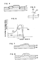
- Fig. 5 shows the relation between a sample 101 to be sputtered on and incident particles 104, or the condition in which particles 104 are incident to the sample 101 at angle ⁇ (incident angle) with respect to the normal 102 to the sample surface.
- Fig. 6 shows the relation between the sputter etching speed and incident angle ( ⁇ ) of particles, or a curve 105.
- a straight line 106 represents the depositing speed of particles to be deposited onto the substrate. If, now, a bias voltage is applied to the substrate holder, the relative speed 105 at which the deposited film is sputter-etched, intersects the depositing speed 106 of particles onto the substrate at 107, so that two regions 108 and 109 are produced with the boundary at the intersection.
- Figs. 7 to 9 show such state of deposition: Fig. 7 shows the initial state, Fig. 8 the midway state and Fig. 9 the completed state.
- a silicon substrate in which switching circuits, scanning circuits and the like are formed, is first prepared.
- the switching circuits and so on are satisfactorily formed in the semiconductor substrate by the normal process for semiconductor devices.
- Fig. 2 is a cross-section of the semiconductor substrate of a photoelectric transducer using a MOS field effect transistor as a switching element for one picture element region.
- Reference numeral 20 represents the P-type silicon substrate, 21 an impurity region provided for good isolation between elements, 22 an insulating film such as Si0 2 , 23 and 24 the impurity deffused regions as source and drain regions, respectively, 25 an insulating film such as Si0 2 , 26 the drain electrode, 27 an interlayer insulating film, 28 the source electrode, and 29 and 30 the gate electrode and a gate insulating film.
- a semiconductor substrate 40 prepared is placed on the substrate holder of the sputtering apparatus, and a bias voltage is applied to the sample holder, during which the photoconductive film 31 is formed by the sputtering method.
- the thickness of the photoconductive film 31 is generally in the range from 0.5 to 4 ⁇ m, or preferably about from 1.5 to 3.0 ⁇ m.
- the transparent electrode 32 is formed on the photoconductive film 31, and a second electrode on the other surface of the semiconductor substrate, thus a photoelectric transducer being fablicated.
- the transparent electrode is formed by depositing a film of indium oxide and tin oxide to about 150 ⁇ m thickness, or a very thin film of gold or the like or metal strip film.
- a solid-state image pickup device is completed.
- Fig. 3 is a cross-section of this image pickup device.
- the amorphous silicon containing hydrogen has the following constituents.
- the photoconductive layer is generally from 0.5 ⁇ m to 4 ⁇ m.
- the hydrogen containing amorphous silicon film is formed by the reactive sputtering method as follows.
- a molten silicon or crystal silicon is used as a target in the atmosphere of the mixture of an inert gas, generally argon Ar and a necessary amount of H 2 gas, in which atmosphere glow discharge is caused by direct current or high frequency.
- argon ions Ar are bombarded to the target in the glow discharge to be deposited on the substrate opposite to the target.
- the silicon atoms Si ejected from the target react with hydrogen atoms H to form a desired amorphous silicon Si film containing hydrogen.
- Another inert gas Ne, Kr, or Xn except Ar and PH 3 or B 2 H 5 gas except H 2 gas may be used instead of the mixture gas of Ar and H 2 .
- the discharge gas pressure is selected to be in the range from 8 x 10 -5 to 5 x 10 -2 Torr. For stable discharge it is preferred to select the range from 1 x 10 -4 to 1 x 10 -2 Torr
- the substrate temperature during deposition may be the temperature at which the general sputtering is performed.
- selection is made between 50° and 300°C, and it is preferred to select between 150 and 250 0 C. Selection of too low temperature will cause unstable coupling between Si and H in the hydrogen containing silicon film, resulting in deterioration of the photoconductive characteristics.
- a negative potential is further applied to the substrate holder.
- Fig. 10 is a schematical diagram useful for explaining the bias sputtering apparatus.
- Reference numeral 204 represents a vacuum container generally called a sputter chamber. The air of the sputter chamber is exhausted from an exhaust port 202 to less than 1 x 10 -6 Torr at most. After exhaustion of air, argon and hydrogen are supplied from gas flow inlets 205 and 206 via gas control valves 207 and 208 to the sputter chamber.
- Reference numeral 209 represents a target to be sputtered to and this target 209 is opposed to a substrate holder 201.
- Reference numeral 203 represents substrate heating means such as heater, and 200 is a semiconductor substrate as a sample.
- the substrate holder 201 and target 209 are supplied with a high-frequency power.
- the high frequency power from a high frequency power source 210 (generally 13.56 MHz) is applied to the substrate holder 201 and the target 209 via capacitors 211 and 212.
- the power to be supplied is selected to be in the range from 0.1 to 10 watt/cm 2 , and the ratio of power to be supplied to the substrate to that to the target is generally in the range from 1/1 to 1/10. If the ratio is selected to be in the range from 1/6 to 1/10, the thickness of the photoconductive film is more uniform as shown in Fig. 9, in which a uniform-thickness photoconductive film 113 is formed on the semiconductor substrate 110. In this case, the electric field to be established when the solid state image pickup device operates is satisfactorily uniform in the photoconductive film.
- the ratio of the voltages to be supplied is usually selected to be 1/6 or 1/8.
- the surface itself of the photoconductive film becomes flat from the macrostandpoint, as shown in Fig. 11, in which a photoconductive film 114 of flat surface is formed on the semiconductor substrate 110. Therefore, the transparent electrode is provided with ease on the photoconductive film.
- the electric field strength at each position is different due to ununiform thickness of the film.
- Reference numerals 213 and 214 designate volt meters for the substrate holder and target, respectively.
- a voltage usually in the range from -5 V to -300 V.
- hydrogenerated amorphous silicon layer of about 3 ⁇ m is formed in three hours.
- Fig. 12 shows the dark currents in the photoelectric transducer according to the invention and the conventional counterpart :
- Curve A indicates the conventional and curve B the invention.
- the photoconductive film is an amorphous silicon containing hydrogen silicon (15%) and the thickness is 2.0 ⁇ m. From the figure it will be seen that the photoelectric transducer according to the invention is very excellent in the dark current characteristic. This is chiefly because the breaks of the photoconductive film at the step have been obviated.
- the reactive sputtering may be made by DC (direct current) instead of RF sputter.
- DC direct current
- a voltage of about -2 to -7 kV is applied to the target.
- the other things may be considered substantially the same as above.
- Fig. 13 shows the way in which DC bias is applied.
- Reference numeral 200 represents the sample, 201 the sample holder, 209 the target, 210 the sputtering high-frequency power source, and 214 a biasing DC power source.
- the method of this invention is utilized for first part of the thickness of the photoconductive film, as a sputtered film for deposition enough to flatten the sides of the underlying irregu- larlities, and then the other part of the thickness of the photoconductive film is grown as a second layer by a conventional deposition method for the consideration of photoconductive characteristics.
- the necessary film thickness to be obtained by the method of the invention is in the range from 0.5 to 2.0 p m.
- part of the thickness of the complete photoconductive film may be achieved on the semiconductor substrate by the normal method and then the other part of the thickness by the method of the invention.
- the photoconductive film may be in three or more layers in order to attain the complete thickness, but the photoconductive film must be deposited to a thickness of 0.5 to 2.0 ⁇ m by the method of the invention.
- the method of depositing photoconductive film on a substrate to which a bias is applied may be utilized for the case where a hydrogen containing silicon film is formed by decomposition of SiH 4 or the like in the glow discharge.
- Fig. 14 shows an example of using the glow discharge.
- Reference numeral 300 denotes a sample, 301 a container which can be evacuated to a vacuum, 302 an rf coil, 303 a sample holder, 304 a temperature measuring thermocouple, 305 a heater, 306 an inlet through which an atmosphere gas such as SiH 4 or the like is introduced, 307 a tank for mixing gases and 308 a connection to an exhaust system.
- the method in which decomposition due to glow discharge is utilized may be a normal one.
- Numeral 309 represents a power supply for supplying a bias to the substrate. This bias has an effect similar to that of the sputtering method.
- Ar gas and SiH 4 gas are introduced into the vacuum container.
- Ar gas is not necessarily used.
- the ratio of SiH 4 gas to Ar gas is 10 vol.% or above, and the gas pressure of the row material gas is in the range between 10- 2 to 3 Torr.
- the substrate is maintained at temperature of 200°C and normally a high frequency of 0.2 to 30 MHz is applied to cause glow discharge in the atmosphere so that the hydrogen containing silicon film is formed on the substrate to a thickness of 2.0 ⁇ m.
- bias of -50 V is applied to the substrate to enable an excellent hydrogenated amorphous silicon layer to be formed, and thus a photoelectric transducer with a small dark current can be realized.
Abstract
Description
- This invention relates to an improvement of a photoelectric transducer or solid state image pickup device formed by a photoconductive layer on a semiconductor substrate.
- The principle of the solid state image pickup device is that a plurality of picture elements each having at least a photoelectric transducing portion' are arranged in a matrix shape and information at each picture element is read by XY address system.
- The photoelectric transducing portion of each element is constructed by, for example, directly forming an impurity diffused region in a silicon substrate, or using a photoconductive layer thereon.
- In the example of using a photoconductive film, a scanning circuit with, for example, MOS transistors and so on for XY addressing is formed in a silicon Si substrate and then a photoconductive layer is formed on the upper layer of the silicon Si substrate to build up a light receiving portion. Such a solid state image pickup device is seen in Japanese Patent Laid-Open (Kokai) No. 95720/ 1976, International Electron Devices Meeting, December, 1979, p 134 to 136, and so on. Moreover, a solid state image pickup device utilizing hydrogenerated amorphous silicon for photoconductive layer is disclosed in U.S. Pat. Application Serial No. 66,230.
- The basic idea of this invention is that when a photoconductive layer is deposited on a semiconductor substrate in which a predetermined scanning circuit or the like is formed, by reactive sputtering, or glow discharge CVD (chemical vapor deposition), or under the condition in which at least plasma exists in the atmosphere, a negative bias voltage is applied to the above semiconductor substrate. This processing makes the photoconductive layer be smoothly deposited onto the irregular, or uneven portion of the semiconductor substrate, and thereby prevents the photoconductive layer from breaking, or disconnecting at the irregular portion or surface.
- In other words, this invention proposes a method of producing photoelectric transducer, which is characterized in that in the atmosphere including at least plasma, where a predetermined substrate is placed on a first electrode to which another electrode is opposed and a negative potential is applied, a photoconductive layer is deposited on the substrate.
- The present invention will be apparent from the following detailed description taken in conjunction with the accompanying drawings, in which:
- Fig. 1 shows the principle of the solid state image pickup device;
- Fig. 2 is a cross-sectional view of a semiconductor substrate;
- Fig. 3 is a cross-sectional view of a picture element of a solid state image pickup device using a photoconductive layer;
- Fig. 4 is an explanatory diagram showing the state of a photoconductive layer deposited by the conventional method;
- Fig. 5 is a diagram showing the relation between the substrate and sputtered particles;
- Fig. 6 is.a graph showing the relation between the incident angle of particles and etching speed;
- Figs. 7 to 9 and 11 are explanatory diagrams showing the deposited state by the method of the invention;
- Fig. 10 is a schematical diagram of a sputtering apparatus;
- Fig. 12 shows dark current characteristics;
- Fig. 13 is an explanatory diagram showing the way in which DC bias voltage is applied; and
- Fig. 14 is a schematical diagram of a glow discharging apparatus.
- Fig. 1 shows the principle of the solid state image pickup device. Picture elements 4 are arranged in a checked pattern and read from one by one by the XY address system. The selection of each picture element is performed by a horizontal scanning signal generator 1 and a vertical
scanning signal generator 2. Reference numeral 3 represents a switch connected to each picture element, and 5 an output terminal. Fig. 2 is a schematical cross-section of a picture element to which reference is made in explaining the principle of the solid state image pickup device using a photoconductive layer.Diffused regions silicon Si substrate 20 to serve as the source and drain of the MOS switch.Reference numeral 29 represents a gate electrode of the MOS switch, 26 a drain electrode thereof from which a signal is taken out, and 28 a source electrode thereof. On the top surface of such a switch circuit are formed a photoconductivethin film 31 and atransparent electrode 32 as shown in Fig. 3. The details of Fig. 2 will be described later. Although CCD (charge coupled device) or the like is formed in a silicon substrate for a scanning circuit as in the prior art, this invention can be applied to the scanning circuit independent of its construction. - The
electrode 28 is opposed via thephotoconductive film 31 made of photoconductive substance such as Sb2S3, CdS, As2Se3, or polycrystalline silicon Si, to the transparentconductive film 32 to form a capacitance C the magnitude of which is proportional to the area, S of the electrode. Since the electrodes are separately arranged in a matrix pattern, the capacitances formed on the electrodes are in a matrix shape. These capacitances each having a photoconductivethin film 31 serve as photosensitive elements, i.e., form picture elements. The photosensitive elements can be replaced by an equivalent circuit which is a parallel circuit of a capacitance C and a variable resistance R depending on the light intensity. - When an optical image is focused via a lens onto the surface of the photoconductive layer, the resistances of the photoconductive film are changed in value in proportional to the light intensity of each part of the optical image. Consequently, at one end 7 of the vertical switch 4 appears a voltage change corresponding to the optical image. This voltage variation is derived through
signal output lines 11 and 12 from the output terminal 5, as a video signal. - However, such a photoelectric transducer as described above has a greatly irregular surface of silicon substrate on which a photoconductive film is formed. This is because MOS transistors, CCD or the like are fabricated in the silicon substrate as described previously. The surface irregularity is 1.5 pm, at maximum.
- The photoconductive film is generally formed by vacuum evaporation, sputtering evaporation, reactive sputtering, glow discharge CVD, or the like, but it is affected by the irregularity of the silicon substrate surface to have many breakes and pinholes particularly around most irregularities. Thus, the solid state imager having such a light receiving surface will provide a formed image having a great number of flaws or defects which results in an extremely poor picture quality. In the worst case, a short circuit may be formed between the transparent electrode on the photoconductive film and the lower electrode on the silicon substrate.
- Fig. 4 illustrates this condition. Here,
reference numeral 110 represents a semiconductor substrate in which switching elements and scanning circuits are formed. The irregularities on the substrate are due to the wiring and lead conductors of semiconductor elements and so on. If a photoconductive film is deposited on the irregular surface by the normal process, discontinuous points will easily occur particularly at steps of the semiconductor substrate as shown in Fig. 4 at a layer 111. Therefore, when atransparent electrode 112 is formed on the photoconductive layer 111, the lower electrodes exposed on the substrate will be apt to contact the transparent electrode. - This invention proposes a method of forming a photoconductive film with the above drawbacks obviated.
- The basic idea of this invention is that when a photoconductive layer is deposited on a semiconductor substrate in which a predetermined scanning circuit or the like is formed, by reactive sputtering, or glow discharge CVD (chemical vapor deposition) or under the condition in which at least plasma exists in the atmosphere, a negative bias voltage is applied to the above semiconductor substrate. 'This processing makes the photoconductive layer be smoothly deposited onto the irregular, or uneven portion of the semiconductor substrate, and thereby prevents the photoconductive layer from breaking, or disconnecting at the irregular portion or surface. This invention can also be applied to, for example, ion plating method by which a photoconductive layer is formed.
- The reason why the method of the invention is effective to restrict the occurence of breakes of the deposited photoconductive film at the steps or irregularities of the substrate, or to make the photoconductive film surface flat, will now be described briefly.
- Fig. 5 shows the relation between a
sample 101 to be sputtered on andincident particles 104, or the condition in whichparticles 104 are incident to thesample 101 at angle ø (incident angle) with respect to the normal 102 to the sample surface. Fig. 6 shows the relation between the sputter etching speed and incident angle (ø) of particles, or a curve 105. A straight line 106 represents the depositing speed of particles to be deposited onto the substrate. If, now, a bias voltage is applied to the substrate holder, the relative speed 105 at which the deposited film is sputter-etched, intersects the depositing speed 106 of particles onto the substrate at 107, so that tworegions - This invention will hereinafter be described for the case in which an amorphous silicon containing hydrogen is used as the photoconductive film. Of course, other photoconductive films can be deposited in the atmosphere containing plasma by the method of this invention: for example, various kinds of chalcogen compounds.
- A silicon substrate in which switching circuits, scanning circuits and the like are formed, is first prepared. The switching circuits and so on are satisfactorily formed in the semiconductor substrate by the normal process for semiconductor devices.
- Fig. 2 is a cross-section of the semiconductor substrate of a photoelectric transducer using a MOS field effect transistor as a switching element for one picture element region.
Reference numeral 20 represents the P-type silicon substrate, 21 an impurity region provided for good isolation between elements, 22 an insulating film such as Si02, 23 and 24 the impurity deffused regions as source and drain regions, respectively, 25 an insulating film such as Si02, 26 the drain electrode, 27 an interlayer insulating film, 28 the source electrode, and 29 and 30 the gate electrode and a gate insulating film. - A
semiconductor substrate 40 prepared is placed on the substrate holder of the sputtering apparatus, and a bias voltage is applied to the sample holder, during which thephotoconductive film 31 is formed by the sputtering method. The thickness of thephotoconductive film 31 is generally in the range from 0.5 to 4 µm, or preferably about from 1.5 to 3.0 µm. Moreover, thetransparent electrode 32 is formed on thephotoconductive film 31, and a second electrode on the other surface of the semiconductor substrate, thus a photoelectric transducer being fablicated. The transparent electrode is formed by depositing a film of indium oxide and tin oxide to about 150 µm thickness, or a very thin film of gold or the like or metal strip film. On a part of the transparent electrode but not the light receiving portion is evaporated via a mask, Cr-Au compound, and to the evaporated area is wire-bonded a biasing electrode. Thus, a solid-state image pickup device is completed. Fig. 3 is a cross-section of this image pickup device. - The sputtering process using biasing according to the invention will be described below.
- The amorphous silicon containing hydrogen has the following constituents.
- It contains 50-atom percent or above silicon and 5-to-50 atom percent hydrogen. The hydrogen content is preferably 5 to 30 atom percent. The silicon may be replaced by Ge or C to about 30% in general. The thickness of the photoconductive layer is generally from 0.5 µm to 4 µm.
- Of course, an impurity is added as necessary.
- The hydrogen containing amorphous silicon film is formed by the reactive sputtering method as follows. A molten silicon or crystal silicon is used as a target in the atmosphere of the mixture of an inert gas, generally argon Ar and a necessary amount of H2 gas, in which atmosphere glow discharge is caused by direct current or high frequency. Thus, argon ions Ar are bombarded to the target in the glow discharge to be deposited on the substrate opposite to the target. The silicon atoms Si ejected from the target react with hydrogen atoms H to form a desired amorphous silicon Si film containing hydrogen. Another inert gas Ne, Kr, or Xn except Ar and PH3 or B2H5 gas except H2 gas may be used instead of the mixture gas of Ar and H2. The discharge gas pressure is selected to be in the range from 8 x 10⁻⁵ to 5 x 10⁻² Torr. For stable discharge it is preferred to select the range from 1 x 10⁻⁴ to 1 x 10⁻² Torr.
- The substrate temperature during deposition may be the temperature at which the general sputtering is performed. For the hydrogen containing silicon, selection is made between 50° and 300°C, and it is preferred to select between 150 and 2500C. Selection of too low temperature will cause unstable coupling between Si and H in the hydrogen containing silicon film, resulting in deterioration of the photoconductive characteristics.
- In this invention, a negative potential is further applied to the substrate holder.
- Fig. 10 is a schematical diagram useful for explaining the bias sputtering apparatus.
Reference numeral 204 represents a vacuum container generally called a sputter chamber. The air of the sputter chamber is exhausted from anexhaust port 202 to less than 1 x 10⁻⁶ Torr at most. After exhaustion of air, argon and hydrogen are supplied from gas flow inlets 205 and 206 viagas control valves Reference numeral 209 represents a target to be sputtered to and thistarget 209 is opposed to asubstrate holder 201.Reference numeral 203 represents substrate heating means such as heater, and 200 is a semiconductor substrate as a sample. During sputtering, thesubstrate holder 201 andtarget 209 are supplied with a high-frequency power. Usually, the high frequency power from a high frequency power source 210 (generally 13.56 MHz) is applied to thesubstrate holder 201 and thetarget 209 viacapacitors 211 and 212. The power to be supplied is selected to be in the range from 0.1 to 10 watt/cm2, and the ratio of power to be supplied to the substrate to that to the target is generally in the range from 1/1 to 1/10. If the ratio is selected to be in the range from 1/6 to 1/10, the thickness of the photoconductive film is more uniform as shown in Fig. 9, in which a uniform-thickness photoconductive film 113 is formed on thesemiconductor substrate 110. In this case, the electric field to be established when the solid state image pickup device operates is satisfactorily uniform in the photoconductive film. The ratio of the voltages to be supplied is usually selected to be 1/6 or 1/8. - On the other hand, as the voltage ratio approaches to 1/1, the surface itself of the photoconductive film becomes flat from the macrostandpoint, as shown in Fig. 11, in which a
photoconductive film 114 of flat surface is formed on thesemiconductor substrate 110. Therefore, the transparent electrode is provided with ease on the photoconductive film. However, when a voltage is applied to thephotoconductive film 114, the electric field strength at each position is different due to ununiform thickness of the film. -
Reference numerals - Fig. 12 shows the dark currents in the photoelectric transducer according to the invention and the conventional counterpart : Curve A indicates the conventional and curve B the invention. The photoconductive film is an amorphous silicon containing hydrogen silicon (15%) and the thickness is 2.0 µm. From the figure it will be seen that the photoelectric transducer according to the invention is very excellent in the dark current characteristic. This is chiefly because the breaks of the photoconductive film at the step have been obviated.
- The reactive sputtering may be made by DC (direct current) instead of RF sputter. For this DC reactive sputtering a voltage of about -2 to -7 kV is applied to the target. The other things may be considered substantially the same as above. Fig. 13 shows the way in which DC bias is applied.
Reference numeral 200 represents the sample, 201 the sample holder, 209 the target, 210 the sputtering high-frequency power source, and 214 a biasing DC power source. - In order that the photoconductive film of the photoelectric transducer or solid state image pickup device has a requisite thickness for flat surface, it is unnecessary to make full use of the method of the invention. For example, the method of this invention is utilized for first part of the thickness of the photoconductive film, as a sputtered film for deposition enough to flatten the sides of the underlying irregu- larlities, and then the other part of the thickness of the photoconductive film is grown as a second layer by a conventional deposition method for the consideration of photoconductive characteristics. In this case, the necessary film thickness to be obtained by the method of the invention is in the range from 0.5 to 2.0 pm.
- On the contrary, part of the thickness of the complete photoconductive film may be achieved on the semiconductor substrate by the normal method and then the other part of the thickness by the method of the invention. Of course, the photoconductive film may be in three or more layers in order to attain the complete thickness, but the photoconductive film must be deposited to a thickness of 0.5 to 2.0 µm by the method of the invention.
- The method of depositing photoconductive film on a substrate to which a bias is applied may be utilized for the case where a hydrogen containing silicon film is formed by decomposition of SiH4 or the like in the glow discharge. Fig. 14 shows an example of using the glow discharge.
Reference numeral 300 denotes a sample, 301 a container which can be evacuated to a vacuum, 302 an rf coil, 303 a sample holder, 304 a temperature measuring thermocouple, 305 a heater, 306 an inlet through which an atmosphere gas such as SiH4 or the like is introduced, 307 a tank for mixing gases and 308 a connection to an exhaust system. The method in which decomposition due to glow discharge is utilized, may be a normal one.Numeral 309 represents a power supply for supplying a bias to the substrate. This bias has an effect similar to that of the sputtering method. - Ar gas and SiH4 gas are introduced into the vacuum container. In this case, Ar gas is not necessarily used. The ratio of SiH4 gas to Ar gas is 10 vol.% or above, and the gas pressure of the row material gas is in the range between 10-2 to 3 Torr. The substrate is maintained at temperature of 200°C and normally a high frequency of 0.2 to 30 MHz is applied to cause glow discharge in the atmosphere so that the hydrogen containing silicon film is formed on the substrate to a thickness of 2.0 µm. The subsequent processes are similar to the above example. Also in this case, bias of -50 V is applied to the substrate to enable an excellent hydrogenated amorphous silicon layer to be formed, and thus a photoelectric transducer with a small dark current can be realized.
Claims (6)
characterized in that:
during at least part of the deposition process to form said photoconductive layer, the substrate is placed on a.first electrode (201) to which is applied a negative potential relative to a second electrode (209) opposed to said first electrode.
Applications Claiming Priority (2)
| Application Number | Priority Date | Filing Date | Title |
|---|---|---|---|
| JP36056/80 | 1980-03-24 | ||
| JP3605680A JPS56133884A (en) | 1980-03-24 | 1980-03-24 | Manufacture of photoelectric transducer |
Publications (3)
| Publication Number | Publication Date |
|---|---|
| EP0036780A2 true EP0036780A2 (en) | 1981-09-30 |
| EP0036780A3 EP0036780A3 (en) | 1982-08-04 |
| EP0036780B1 EP0036780B1 (en) | 1986-06-18 |
Family
ID=12459052
Family Applications (1)
| Application Number | Title | Priority Date | Filing Date |
|---|---|---|---|
| EP81301239A Expired EP0036780B1 (en) | 1980-03-24 | 1981-03-23 | Method of producing photoelectric transducers |
Country Status (5)
| Country | Link |
|---|---|
| US (1) | US4430185A (en) |
| EP (1) | EP0036780B1 (en) |
| JP (1) | JPS56133884A (en) |
| CA (1) | CA1167951A (en) |
| DE (1) | DE3174837D1 (en) |
Cited By (2)
| Publication number | Priority date | Publication date | Assignee | Title |
|---|---|---|---|---|
| EP0087151A2 (en) * | 1982-02-23 | 1983-08-31 | Siemens Aktiengesellschaft | Process for producing layers of refractory metals or metallic compounds by chemical vapour deposition |
| WO2020173985A1 (en) * | 2019-02-27 | 2020-09-03 | Trinamix Gmbh | Optical sensor and detector for an optical detection |
Families Citing this family (16)
| Publication number | Priority date | Publication date | Assignee | Title |
|---|---|---|---|---|
| DE3429899A1 (en) * | 1983-08-16 | 1985-03-07 | Canon K.K., Tokio/Tokyo | METHOD FOR FORMING A DEPOSITION FILM |
| DE3417732A1 (en) * | 1984-05-12 | 1986-07-10 | Leybold-Heraeus GmbH, 5000 Köln | METHOD FOR APPLYING SILICON-CONTAINING LAYERS TO SUBSTRATES BY CATODIZING AND SPRAYING CATODE FOR CARRYING OUT THE METHOD |
| JPS617624A (en) * | 1984-06-22 | 1986-01-14 | Fuji Xerox Co Ltd | Formation of amorphous semiconductor layer |
| US4759947A (en) * | 1984-10-08 | 1988-07-26 | Canon Kabushiki Kaisha | Method for forming deposition film using Si compound and active species from carbon and halogen compound |
| US4726963A (en) * | 1985-02-19 | 1988-02-23 | Canon Kabushiki Kaisha | Process for forming deposited film |
| US5244698A (en) * | 1985-02-21 | 1993-09-14 | Canon Kabushiki Kaisha | Process for forming deposited film |
| US4818563A (en) * | 1985-02-21 | 1989-04-04 | Canon Kabushiki Kaisha | Process for forming deposited film |
| JPS61223756A (en) * | 1985-03-28 | 1986-10-04 | Canon Inc | Copying machine |
| US4853251A (en) * | 1985-02-22 | 1989-08-01 | Canon Kabushiki Kaisha | Process for forming deposited film including carbon as a constituent element |
| US4801468A (en) * | 1985-02-25 | 1989-01-31 | Canon Kabushiki Kaisha | Process for forming deposited film |
| JP2537175B2 (en) * | 1985-03-27 | 1996-09-25 | キヤノン株式会社 | Functional deposition film manufacturing equipment |
| JPH0647727B2 (en) * | 1985-12-24 | 1994-06-22 | キヤノン株式会社 | Deposited film formation method |
| JPH084071B2 (en) * | 1985-12-28 | 1996-01-17 | キヤノン株式会社 | Deposited film formation method |
| US6197471B1 (en) * | 1998-03-25 | 2001-03-06 | Coulter International Corp. | Amorphous silicon photoreceptor and method for making same |
| IL153895A (en) * | 2003-01-12 | 2013-01-31 | Orion Solar Systems Ltd | Solar cell device |
| JP4497068B2 (en) * | 2005-09-26 | 2010-07-07 | 日新電機株式会社 | Silicon dot forming method and silicon dot forming apparatus |
Citations (5)
| Publication number | Priority date | Publication date | Assignee | Title |
|---|---|---|---|---|
| FR2014490A1 (en) * | 1968-07-03 | 1970-04-17 | Ibm | |
| FR2119930A1 (en) * | 1970-12-31 | 1972-08-11 | Ibm | |
| US4086555A (en) * | 1976-05-27 | 1978-04-25 | General Dynamics Corporation | Photoconductive sensor |
| FR2371524A1 (en) * | 1976-11-18 | 1978-06-16 | Alsthom Atlantique | PROCESS FOR DEPOSITING A THIN LAYER BY DECOMPOSITION OF A GAS IN A PLASMA |
| FR2433871A1 (en) * | 1978-08-18 | 1980-03-14 | Hitachi Ltd | SEMICONDUCTOR IMAGE FORMING DEVICE |
-
1980
- 1980-03-24 JP JP3605680A patent/JPS56133884A/en active Pending
-
1981
- 1981-03-20 CA CA000373556A patent/CA1167951A/en not_active Expired
- 1981-03-20 US US06/245,749 patent/US4430185A/en not_active Expired - Fee Related
- 1981-03-23 DE DE8181301239T patent/DE3174837D1/en not_active Expired
- 1981-03-23 EP EP81301239A patent/EP0036780B1/en not_active Expired
Patent Citations (5)
| Publication number | Priority date | Publication date | Assignee | Title |
|---|---|---|---|---|
| FR2014490A1 (en) * | 1968-07-03 | 1970-04-17 | Ibm | |
| FR2119930A1 (en) * | 1970-12-31 | 1972-08-11 | Ibm | |
| US4086555A (en) * | 1976-05-27 | 1978-04-25 | General Dynamics Corporation | Photoconductive sensor |
| FR2371524A1 (en) * | 1976-11-18 | 1978-06-16 | Alsthom Atlantique | PROCESS FOR DEPOSITING A THIN LAYER BY DECOMPOSITION OF A GAS IN A PLASMA |
| FR2433871A1 (en) * | 1978-08-18 | 1980-03-14 | Hitachi Ltd | SEMICONDUCTOR IMAGE FORMING DEVICE |
Non-Patent Citations (2)
| Title |
|---|
| METAL FINISHING, vol. 72 no. 3, March 1974. HACKENSAR New York (USA); L.B.LEDER: "Fundamental Parameters of Ion Plating", pages 41-45 * |
| SOLID STATE TECHNOLOGY, vol. 13 no. 12, December 1970. Port Washington New York (USA); O. CHRISTENSEN: "Characteristics and applications of bios sputtering", pages 39-45 * |
Cited By (4)
| Publication number | Priority date | Publication date | Assignee | Title |
|---|---|---|---|---|
| EP0087151A2 (en) * | 1982-02-23 | 1983-08-31 | Siemens Aktiengesellschaft | Process for producing layers of refractory metals or metallic compounds by chemical vapour deposition |
| EP0087151A3 (en) * | 1982-02-23 | 1984-07-25 | Siemens Aktiengesellschaft | Process for producing layers of refractory metals or metallic compounds by chemical vapour deposition |
| WO2020173985A1 (en) * | 2019-02-27 | 2020-09-03 | Trinamix Gmbh | Optical sensor and detector for an optical detection |
| US11908956B2 (en) | 2019-02-27 | 2024-02-20 | Trinamix Gmbh | Optical sensor and detector for an optical detection |
Also Published As
| Publication number | Publication date |
|---|---|
| US4430185A (en) | 1984-02-07 |
| EP0036780B1 (en) | 1986-06-18 |
| DE3174837D1 (en) | 1986-07-24 |
| JPS56133884A (en) | 1981-10-20 |
| CA1167951A (en) | 1984-05-22 |
| EP0036780A3 (en) | 1982-08-04 |
Similar Documents
| Publication | Publication Date | Title |
|---|---|---|
| US4430185A (en) | Method of producing photoelectric transducers | |
| US4360821A (en) | Solid-state imaging device | |
| US4814842A (en) | Thin film transistor utilizing hydrogenated polycrystalline silicon | |
| US5589233A (en) | Single chamber CVD process for thin film transistors | |
| US5420044A (en) | Method for producing non-monocrystalline semiconductor device | |
| US4797108A (en) | Method of manufacturing amorphous silicon field effect transistors | |
| CA1161534A (en) | Photoelectric converter | |
| EP0082783B1 (en) | Process for manufacturing silicon thin-film transistors on an insulating substrate | |
| EP0047651A1 (en) | Method of producing image sensor | |
| EP0045203B1 (en) | Method of producing an image pickup device | |
| JP3055782B2 (en) | How to manufacture thin film transistors | |
| JPH03263316A (en) | Method of depositing zinc sulfide layer and device therefor | |
| KR840002152B1 (en) | The fabrication method in photo device | |
| US4883562A (en) | Method of making a photosensor | |
| KR900001981B1 (en) | Manufacturing method of semiconductor film | |
| JP3201495B2 (en) | Manufacturing method of amorphous silicon | |
| JPH0214790B2 (en) | ||
| JP2854363B2 (en) | Manufacturing method of light receiving element | |
| KR830000704B1 (en) | Solid-state imaging device | |
| JPH0419650B2 (en) | ||
| JP2505662B2 (en) | Method for manufacturing thin film transistor | |
| JPH06130413A (en) | Manufacture of liquid crystal display device | |
| JPS6258675B2 (en) | ||
| JPH0442577A (en) | Thin film transistor | |
| JPS6258676B2 (en) |
Legal Events
| Date | Code | Title | Description |
|---|---|---|---|
| PUAI | Public reference made under article 153(3) epc to a published international application that has entered the european phase |
Free format text: ORIGINAL CODE: 0009012 |
|
| AK | Designated contracting states |
Designated state(s): DE FR GB NL |
|
| RBV | Designated contracting states (corrected) |
Designated state(s): DE FR GB NL |
|
| PUAL | Search report despatched |
Free format text: ORIGINAL CODE: 0009013 |
|
| AK | Designated contracting states |
Designated state(s): DE FR GB NL |
|
| 17P | Request for examination filed |
Effective date: 19821227 |
|
| GRAA | (expected) grant |
Free format text: ORIGINAL CODE: 0009210 |
|
| AK | Designated contracting states |
Kind code of ref document: B1 Designated state(s): DE FR GB NL |
|
| REF | Corresponds to: |
Ref document number: 3174837 Country of ref document: DE Date of ref document: 19860724 |
|
| ET | Fr: translation filed | ||
| PLBE | No opposition filed within time limit |
Free format text: ORIGINAL CODE: 0009261 |
|
| STAA | Information on the status of an ep patent application or granted ep patent |
Free format text: STATUS: NO OPPOSITION FILED WITHIN TIME LIMIT |
|
| 26N | No opposition filed | ||
| PGFP | Annual fee paid to national office [announced via postgrant information from national office to epo] |
Ref country code: FR Payment date: 19891222 Year of fee payment: 10 |
|
| PGFP | Annual fee paid to national office [announced via postgrant information from national office to epo] |
Ref country code: GB Payment date: 19891231 Year of fee payment: 10 |
|
| PGFP | Annual fee paid to national office [announced via postgrant information from national office to epo] |
Ref country code: DE Payment date: 19900330 Year of fee payment: 10 |
|
| PGFP | Annual fee paid to national office [announced via postgrant information from national office to epo] |
Ref country code: NL Payment date: 19900331 Year of fee payment: 10 |
|
| PG25 | Lapsed in a contracting state [announced via postgrant information from national office to epo] |
Ref country code: GB Effective date: 19910323 |
|
| PG25 | Lapsed in a contracting state [announced via postgrant information from national office to epo] |
Ref country code: NL Effective date: 19911001 |
|
| NLV4 | Nl: lapsed or anulled due to non-payment of the annual fee | ||
| GBPC | Gb: european patent ceased through non-payment of renewal fee | ||
| PG25 | Lapsed in a contracting state [announced via postgrant information from national office to epo] |
Ref country code: FR Effective date: 19911129 |
|
| PG25 | Lapsed in a contracting state [announced via postgrant information from national office to epo] |
Ref country code: DE Effective date: 19920101 |
|
| REG | Reference to a national code |
Ref country code: FR Ref legal event code: ST |