EP0030136B1 - Geregelte Ablenkschaltung mit Anlaufsteuerung - Google Patents
Geregelte Ablenkschaltung mit Anlaufsteuerung Download PDFInfo
- Publication number
- EP0030136B1 EP0030136B1 EP19800304277 EP80304277A EP0030136B1 EP 0030136 B1 EP0030136 B1 EP 0030136B1 EP 19800304277 EP19800304277 EP 19800304277 EP 80304277 A EP80304277 A EP 80304277A EP 0030136 B1 EP0030136 B1 EP 0030136B1
- Authority
- EP
- European Patent Office
- Prior art keywords
- deflection
- voltage
- circuit
- winding
- switch
- Prior art date
- Legal status (The legal status is an assumption and is not a legal conclusion. Google has not performed a legal analysis and makes no representation as to the accuracy of the status listed.)
- Expired
Links
Images


Classifications
-
- H—ELECTRICITY
- H04—ELECTRIC COMMUNICATION TECHNIQUE
- H04N—PICTORIAL COMMUNICATION, e.g. TELEVISION
- H04N3/00—Scanning details of television systems; Combination thereof with generation of supply voltages
- H04N3/10—Scanning details of television systems; Combination thereof with generation of supply voltages by means not exclusively optical-mechanical
- H04N3/16—Scanning details of television systems; Combination thereof with generation of supply voltages by means not exclusively optical-mechanical by deflecting electron beam in cathode-ray tube, e.g. scanning corrections
- H04N3/18—Generation of supply voltages, in combination with electron beam deflecting
- H04N3/185—Maintaining dc voltage constant
Definitions
- This invention relates to regulated deflection circuits.
- Switching regulators for television receiver power supplies may conveniently provide AC power line or mains supply isolation at the input transformer of the switching regulator.
- the flyback transformer may provide mains supply isolation, with the flyback transformer functioning as the switching supply input transformer.
- the regulator switch is located in the non-isolated section of the power supply and is coupled in series with the primary winding of the flyback transformer across the mains supply source.
- the horizontal deflection generator including the horizontal deflection winding is coupled to a conductively isolated secondary winding of the flyback transformer.
- the regulator switch is turned on at a controlled instant within the trace interval of each horizontal deflection cycle to draw input current in the flyback transformer primary winding from the mains supply.
- the energy stored in the flyback transformer during conduction of the regulator switch within the horizontal trace interval is transferred during retrace to secondary winding load circuits such as the horizontal deflection generator and the high voltage ultor load.
- a transistor is used as the regulator switch.
- a control circuit provides a reverse bias voltage to the base of the transistor, either toward the end of the trace interval or during the retrace interval, to turn the transistor off.
- Such a regulator circuit has the disadvantage of requiring a relatively complex control circuit to maintain the transistor conducting during trace and to turn off the transistor without undue dissipation or damage during turn-off.
- a thyristor such as a silicon controlled rectifier
- a relatively simple control circuit turns on the thyristor within the trace interval.
- An LC commutating circuit is coupled to the thyristor and initiates a resonant current oscillation upon thyristor turn-on.
- the thyristor is commutated off as the resonant current provided by the commutating circuit attempts to reverse direction in the thyristor.
- Such a circuit has the disadvantage of using a relatively costly inductor as part of the commutating circuit.
- additional circuitry is desirable for slow start-up of the regulated deflection circuit and for electronic circuit breaker operation during overload and short-circuit conditions.
- a slow start mode of operation is desirable upon initial energization of the regulated deflection circuit because the retrace pulse voltage used to commutate off the thyristor switch is initially absent or of too low an amplitude.
- An electronic circuit breaker function is desirable to disable the regulator during short-circuit and overload conditions when the retrace pulse voltage is absent or insufficient to properly commutate off the regulator switch thyristor.
- a regulated deflection circuit is known from US Patent 4,146,823.
- a regulated deflection circuit with start-up circuitry comprising: a deflection winding; a deflection generator coupled to said deflection winding for generating scanning current in said deflection winding, a deflection rate voltage with an alternating polarity component voltage being developed at a deflection generator terminal; a source of supply frequency alternating polarity voltage; a controllable regulator switch; an input transformer with first and second windings, said first winding being coupled to said source and to said regulator switch for transferring energy from said source to a load circuit coupled to a winding of said input transformer other than said first winding in accordance with the conduction time of said regulator switch, said second winding being coupled to said deflection generator terminal; a regulator control circuit coupled to said regulator switch for turning on said regulator switch at a controlled instant within a first polarity interval of said deflection rate alternating polarity component voltage, to draw current in said first winding from said source, said deflection rate alternating polarity component
- An embodiment of the invention comprises means for inhibiting the generation of the second switch turn-on signals for a predetermined interval upon initiation of the start-up interval.
- Such an inhibit interval is desirable to prevent transient voltages generated after the initial energization of the deflection circuit from improperly turning on the second switch at instants other than near the zero-crossover instant.
- the output of a flip-flop having two output state voltages is applied to the control circuit of the second switch.
- the flip-flop Upon initiation of the start-up interval, the flip-flop develops the first output state voltage and inhibits the generation of the second switch turn-on signal.
- the flip-flop changes output states and applies the second output voltage to the second switch control circuit to enable the generation of the second switch turn-on signal.
- An embodiment of the invention comprises means for applying a deflection rate signal to the second switch control circuit during steady-state operation of the deflection circuit so as to generate the second switch turn-on signal during each cycle of horizontal deflection, thereby ensuring the turn-on of the second switch as soon as the main supply voltage permits forward conduction through the switch.
- the second switch functions as an electronic circuit breaker to block the flow of input current from the mains supply during deflection circuit overload or short-circuit conditions.
- a signal representative of the amplitude of the deflection rate voltage, such as a retrace pulse voltage, used to vary the instant of turn-on the regulator switch is sensed by the electronic circuit breaker circuit.
- a sharp transition occurring in the sensed signal which indicates that an overload or short-circuit condition has occurred, trips the circuit breaker.
- the inhibit flip-flop switches back to the first output state voltage, thereby preventing the second switch turn-on signal from being generated and thereby blocking the flow of input current.
- means are provided to precharge the trace capacitor or the DC blocking capacitor that is coupled to the deflection generator coupled flyback transformer secondary winding.
- the trace or DC blocking capacitor is precharged prior to the initial conduction of the regulator switch so as to enable the generation of minimum amplitude retrace pulses for commutating off the regulator switch during start-up.
- a fuse 84 and a mechanical on-off switch 83 are coupled between source 21 and input terminal 23.
- a terminal 25 of full-wave bridge rectifier 26 comprises the current return or non-isolated ground terminal.
- An output terminal 24 of full-wave bridge rectifier 26 is coupled through the anode-to-cathode path of a controllable switch, SCR 27, to an end terminal 28 of the primary winding 30a of an input transformer 30.
- a filter capacitor 29 is coupled to end terminal 28 to develop a filtered but unregulated DC input voltage Vin at terminal 28.
- the other end terminal of input transformer primary winding 30a is coupled to the anode of controllable regulator switch SCR 76.
- the cathode of SCR 76 is coupled to non-isolated ground.
- SCR 76 and diode 77 may comprise a single semiconductor element 75 such as an integrated thyristor-rectifier (ITR).
- Input transformer 30 may comprise a horizontal output of flyback transformer with a rectangular core 130.
- Primary winding 30a is wound around one leg of rectangular core 130 and secondary windings 30b-30d may be wound around the opposite leg.
- secondary windings 30b-30d may be wound around the opposite leg.
- a substantial leakage inductance 230 due to loose magnetic coupling, exists between primary winding 30a and each of the second windings 30b-30d.
- the secondary windings are relatively tightly coupled to each other magnetically and a relatively small leakage inductance exists between any two of the secondary windings.
- An end terminal of flyback transformer secondary winding 30b is coupled to a horizontal deflection generator 48 at the collector of a horizontal output transistor 49.
- a DC blocking capacitor 47 is coupled to the other end terminal of secondary winding 30b.
- Horizontal deflection generator 48 comprises the series arrangement of a horizontal deflection winding 53 and an S-shaping or trace capacitor 52, a retrace capacitor 51, and trace switch 54 comprising horizontal output transistor 49 and a damper diode 50.
- a conventional horizontal oscillator 55 provides a square-wave switching voltage 56, repeating at the horizontal deflection frequency, 1/T H , to a horizontal driver 57 for switching horizontal output transistor 49 into conduction within the horizontal trace interval of each deflection cycle and for cutting off the output transistor to initiate the horizontal retrace interval.
- a +15 volt DC supply voltage is applied to horizontal oscillator 55 at a terminal L and a +25 volt DC supply voltage is applied to horizontal driver 57 at a terminal M.
- the retrace pulse voltage Vr developed by deflection generator 48 at the collector of horizontal output transistor 49 is applied to flyback transformer secondary winding 30b, stepped up in voltage by high voltage secondary winding 30d, rectified by a diode 45 and filtered by a capacitor 46 to develop an ultor accelerating potential at a terminal U for the ultor load, not shown, of a television receiver picture tube.
- the retrace pulse voltage developed in flyback transformer secondary winding 30c is rectified by a diode 42 that is coupled to an end conductor lead 35 and filtered by a capacitor 43 to develop a +230 volt DC supply voltage at a terminal 44.
- the voltage developed across flyback transformer secondary winding 30c is rectified during the trace interval by a diode 36 that is coupled to the other end conductor lead 31 and is filtered by a capacitor 37 to develop a +25 volt DC supply voltage at a terminal 38.
- a rectifier 39 is coupled to a tap terminal 32 of secondary winding 30c to developed a +15 volt DC supply voltage at a terminal 41 after filtering by a capacitor 40.
- a tap terminal 33 is coupled to a chassis ground conductively isolated from the earth ground which is coupled to primary winding 30a.
- a separate mains rectified auxiliary power supply 85 comprising an auxiliary mains supply transformer 62, a bridge rectifier 63, a diode 65 and a filter capacitor 66, provides +24 volts DC at a terminal 67.
- the +24 volts DC is used as a start-up supply, as will be explained, and also powers, for example, a high wattage audio circuit, not illustrated in FIGURE 1.
- Regulator SCR 76 is gated into conduction at a controlled instant within the trace interval of each horizontal deflection cycle by a gating pulse 78 developed by a regulator circuit 58.
- the gating pulse 78 is coupled by a transformer 60 to the gate of the SCR through a capacitor 70.
- a primary winding current i flows in transformer winding 30a and in SCR 76.
- a deflection circuit energy level such as the retrace pulse amplitude Vr
- the turn-on instant of SCR 76 and, thus, its conduction time is varied by regulator control circuit 58 in response to variations of the deflection circuit level as represented by the retrace pulse 79 developed at a tap terminal 34 of secondary winding 30c and applied to the regulator control circuit along a conductor line 80.
- Operation of regulator circuit 58 is synchronized with horizontal deflection during start-up by applying to the regulator along a conductor line 81 the square-wave switching voltage 56 developed by horizontal oscillator 55, and is synchronized during steady-state operation by the applied retrace pulse 79.
- the turn-on instant of regulator SCR 76 within the interval t1 a-t1 d is varied during the horizontal trace interval under varying load and mains supply voltage conditions to produce waveforms such as waveforms 71-74 representing the current i, flowing in primary winding 30a and ITR 75.
- the turn-on of SCR 76 varies from the instant t1 a for waveform 71 to the instant t1 for waveform 74.
- the current i increases from the turn-on instant of the SCR. until the instant t 3 , within the retrace interval, is reached.
- the retrace pulse voltage Vr that is developed at the collector of horizontal output transistor 49 beginning at time t2 is applied to flyback transformer secondary winding 30b to reflect a resonating current to primary winding 30a such that the current i i in winding 30a begins to decrease in a resonant manner beginning at time t3.
- the current i Near the center of the horizontal retrace interval, the current i, reverses direction and commutates off SCR 76.
- the negative current i is then carried by diode 77 to return energy to terminal 28.
- the current i again flows as 2 positive-going but negatively- valued ramp until the zero current level is reached, at which time diode 77 is commutated off and the ITR becomes an open- circuit.
- Transformer 30 Energy is transferred by way of transformer 30 to the load circuits such as the ultor load during the horizontal retrace interval, as indicated by the peak magnitude of the positive current i, near the beginning of horizontal retrace being greater than the peak magnitude of the negative current near the end of horizontal retrace.
- the energy transferred during horizontal retrace is stored in the leakage inductance 230 of transformer 30.
- Transformer 30 is designed to provide sufficient leakage inductance to store all of the required energy that is to be transferred under normal deflection circuit operation while still enabling the current i 1 to become negative during horizontal retrace in order to commutate off SCR 76.
- the amount of energy stored and transferred is a function of the conduction time of SCR 76 and ITR 75.
- a feature of the invention is to ensure proper commutation of regulator SCR 76 during the start-up interval after closure of on-off switch 83 when the retrace pulse voltage Vr is absent or is of insufficient amplitude to reflect sufficient resonant current to primary winding 30a for commutation purposes.
- the start-up circuit for deflection circuit 20 includes SCR 27 and a control circuit 59 for providing turn-on gating pulses to SCR 27 by way of a transformer 61 and a capacitor 69.
- DC blocking capacitor 47 and trace capacitor 52 are precharged through a diode 68 from the 24 volt supply terminal 67 of auxiliary supply 85 to the initial conduction of regulator SCR 76.
- This precharging enables the immediate generation of relatively low amplitude retrace pulses Vr when horizontal oscillator 55 begins to provide the square-wave switching voltage 56.
- the current i, in primary winding 30a is maintained at a relatively small value in order to permit the low amplitude retrace pulse voltage Vr during start-up to commutate off regulator SCR 76.
- control circuit 59 initially provides gating pulses to SCR 27 immediately prior to the zero-crossover instants of the alternating polarity mains supply voltage.
- the full-wave rectified mains voltage V 64 is applied to control circuit 59 from terminal 64 along a conductor line 82.
- SCR 27 By turning on SCR 27 immediately prior to the zero-crossover instants of the mains supply voltage, the conduction time of SCR 27 is kept relatively short. A relatively small amount of input current flows from mains supply 21, resulting in a relatively low input voltage Vin being developed at terminal 28 and a relatively small current i, flowing in primary winding 30a. SCR 76 can therefore be commutated off during the start-up interval when the retrace pulse voltage amplitude is relatively small. Control circuit 59 then phase advances the gating of SCR 27 away from the zero-crossover instants during the transition from start-up to steady-state operation to enable greater amounts of input current to flow and to bring the input voltage Vin to its steady-state value.
- Another feature of the invention is to combine an electronic circuit breaker function with the start-up function of SCR 27. If a transformer secondary winding coupled load, such as the ultor load, short circuits and substantially reduces the amplitude of the retrace pulse voltage Vr, or if, for example, deflection generator 48 malfunctions and fails to generate a retrace pulse voltage, regulator SCR 76 will not be commutated off. To prevent the current i, in flyback transformer primary winding 30a from increasing to prohibitive values under a shortcircuited secondary load condition or a malfunctioning deflection generator condition, a retrace pulse voltage 79 is applied to control circuit 59 along conductor line 80.
- a transformer secondary winding coupled load such as the ultor load
- Control circuit 59 prevents the generation of gating pulses to SCR 27 when sensing a negative-going transient produced by the collapse of retrace pulse voltage 79.
- the input current path to primary winding 30a from mains supply 21 is then opened up, thereby disabling normal deflection circuit operation.
- control circuit 59 After normal deflection circuit operation is disabled, the start-up portion of control circuit 59 again turns on SCR 27 immediately prior to the zero-crossover instants of the mains supply voltage to repeat the slow start sequence. Should the fault condition persist, the disabling circuit portion of control circuit 59 will again be activated to disable deflection circuit 20. Operation of deflection circuit 20 under a persistent fault condition will cycle between start-up and disabling modes of operation until fuse 84 opens and maintains the deflection circuit disabled.
- control circuit 59 applies a gating pulse to SCR 27 once each horizontal deflection cycle in response to the horizontal deflection rate square-wave voltage 56 applied to control circuit 59 along conductor line 81.
- FIGURE 3 illustrates a portion of the circuit of FIGURE 1 including detailed embodiments of regulator circuit 58 and the start-up and electronic circuit breaker control circuit 59.
- a 15 volt DC voltage at terminal L and a 6.8 volt DC voltage at a terminal N provide operating voltages for the two control circuits.
- a driver transistor Q5 within regulator circuit 58 is switched on at a controlled instant within the trace interval of each deflection cycle to produce gating pulses 78 to turn on regulator SCR 76.
- the exact turn-on instant of transistor Q5 is determined by the triggering of a comparator 90 in accordance with variations in the amplitude of retrace pulse 79 is applied to regulator circuit 58 along conductor line 80.
- comparator 90 is triggered by the leading or positive-going edge of the horizontal deflection rate square-wave switching voltage 56 obtained from horizontal oscillator 55 and applied to input pin 5 of comparator 90 after first being differentiated.
- the leading edge of square-wave switching voltage 56 is also used to turn off horizontal output transistor 49.
- a horizontal rate sawtooth voltage is developed at input pin 6 of comparator 90. This sawtooth voltage is obtained by the integration of flyback pulses 79 by resistor R3 and capacitor C5 after being square-wave shaped by a zener diode D6.
- the sawtooth voltage at pin 6 of comparator 90 advances the triggering of the comparator and the turn-on of SCR 76 relative to the turn-on instant produced by the leading edge of square-wave voltage 56. SCR 76 gradually conducts longer, and increasingly greater amounts of energy are transferred to the flyback transformer secondary winding coupled load circuits until a steady-state equilibrium condition has been achieved.
- a diode D4 rectifies retrace pulse 79 to produce a DC control voltage at a terminal E across a capacitor C4.
- the DC control voltage varies with retrace pulse amplitude variations.
- the DC control voltage is level shifted by a zener diode D5 and combined with the sawtooth voltage at pin 6 of comparator 90 to vary the triggering of comparator 90 and the turn-on of SCR 76 so as to maintain the retrace pulse voltage amplitude relatively constant.
- start-up control circuit 59 initially turns on SCR 27 immediately prior to the zero-crossover instants of the mains supply voltage.
- the full-wave rectified mains supply voltage V 64 illustrated in FIGURE 5a, is applied to an input pin 4 of a comparator 92.
- Comparator 92 inverts and limits the rectified mains supply voltage to produce a square-wave voltage V A , illustrated in FIGURE 5b, at a terminal A, the output pin 2 of comparator 92.
- the positive portion of square-wave voltage V A occurs between times t 1 ⁇ t 4 encompassing the zero-crossover instant t 3 of the full-wave rectified mains supply voltage V B4 .
- Square-wave voltage V A is differentiated by a capacitor 88 and a resistor 89 to produce the voltage V B across resistor 89 at a terminal B, as illustrated in FIGURE 5c.
- the negative differentiated spike portion of the voltage V B occurring at the trailing edge of the square-wave voltage V A at time t 4 is applied to an input pin 6 of monostable switch 93, at a terminal C.
- the voltage at pin 6 of monostable switch 93 is square-wave shaped by a diode D1 to produce the negative pulse voltage V D1 at time t 4 , illustrated in FIGURE 5d.
- the negative-going edge of the pulse V D1 causes the monostable switch 93 to switch output state voltages at output pin 1, at a terminal D. As illustrated in FIGURE 5e, the voltage V D at terminal D goes high at time t 4 .
- the output of monostable switch 93 remains high for a predetermined interval t 4 ⁇ t 8 of FIGURE 5e.
- the duration t 4 -t s of the unstable high output state of monostable switch 93 is determined by the voltage V C1 developed at input pin 6 of monostable switch 93 after the occurrence of the negative pulse V D1' as illustrated in FIGURES 5d and 5e.
- the voltage at pin 6 of monostable switch 93 is determined by the values of voltage dividing resistors 96 and 97 in parallel with resistor 128.
- the negative-going edge at time t 2 or t 8 of the resultant square-wave output voltage V D of monostable 93 is differentiated by the network 120-125 to apply a negative spike voltage 98 to the base of a driver transistor Q4 to turn the transistor on, as illustrated by the base voltage V bQ4 and by the collector voltage V cQ4 of FIGURES 5f and 5g.
- the resultant pulsed collector voltage comprises the gating pulses 179 of FIGURE 5g. Pulses 179 are applied through transformer 61 to turn on SCR 27 at times t 2 and t 8 immediately prior to zero-crossover instants t 3 and tg of the full-wave rectified AC mains voltage V 64 , as required to provide slow start-up operation of deflection circuit 20.
- An inhibit circuit 126 illustrated in FIGURE 3, is included in the control circuit 59 of SCR 27. Inhibit circuit 126 disables the output of monostable switch 93, thereby preventing transistor Q4 for turning on and triggering SCR 27. Inhibit circuit 126 is activated for a predetermined interval, typically around 0.5 to 1 second. After the elapse of this inhibit interval, the output of monostable 93 is no longer disabled, thereby permitting the triggering of SCR 27 immediately prior to a zero-crossover instant of the mains supply voltage.
- Inhibit circuit 126 comprises a flip-flop 95 having an output pin 14 coupled to the output path of monostable switch 93 by way of a diode D3. Immediately after closure of on-off switch 83, the output of flip-flop 95 is low or grounded, thereby grounding F which is coupled to the anode of diode D3. SCR 27 cannot be triggered as long as output pin 14 of flip-flop 95 is in the low or ground state.
- capacitor C3 After approximately 0.8 second, as determined by the time constant of a resistor R2 and a capacitor C3, capacitor C3 has charged sufficiently to raise the voltage at input pin 9 of flip-flop 95 to a value that will cause flip-flop 95 to change output states at pin 14. Diode D3 becomes reverse biased and the output of monostable switch 93 is now permitted to turn on transistor Q4 and trigger SCR 27.
- the output of monostable switch 93 returns to its stable low state at a continuously advancing instant, such as the advanced instant t s , and then the advanced instant t 5 , resulting in the continuous phase advance of the triggering of SCR 27 away from near the zero-crossover instant to the instant t e , for example, and then to the instant t 5 .
- a trigger comparator 91 is enabled and switches transistor Q4 into conduction each horizontal deflection cycle to trigger SCR 27 into conduction each deflection cycle.
- An output pin 1 of comparator 91 is coupled to the base of transistor Q4 through a resistor 129.
- the horizontal deflection rate square-wave switching voltage 56 is applied to the positive input pin terminal 3 of comparator 91 along conductor line 81.
- the increasing voltage developed across capacitor C2 is applied to the inverting input pin 2 of comparator 91.
- the low voltage power supply 180 of FIGURE 1 provides +15 volts DC and +25 volts DC at terminals L and M, respectively, for energizing horizontal oscillator 55, horizontal driver 57, regulator circuit 58, and start-up control circuit 59 during start-up.
- Power supply 180 also provides +6.8 volts DC at terminal N for energizing circuits 58 and 59 both during start-up and steady-state operation.
- a detailed embodiment of power supply 180 is illustrated in FIGURE 6.
- a zener diode 86 maintains the voltage at terminal N at +6.8 volts DC.
- Zener bias is obtained through a resistor 87 from the +24 volts DC at terminal 67 developed by power supply 85.
- the +24 volts at terminal 67 is applied to terminal M through a resistor 181 and a diode 182.
- the start-up voltage at terminal M although less than the steady-state terminal M voltage of +25 volts DC, is sufficient to energize horizontal driver 57 into operation.
- flyback transformer 30 of FIGURE 1 provides +25 volts DC at terminal M of FIGURE 6 through terminal 38 and a diode 183.
- diode 182 is reverse biased, disconnecting power supply 85 from terminal M.
- the +24 volts at terminal 67 is applied to terminal L through resistor 181, a transistor 184 and a diode 185.
- the start-up voltage at terminal L although less than the steady-state terminal L voltage of + 15 volts DC, is sufficient to energize horizontal oscillator 55, regulator circuit 58 and start-up and control circuit 59 into operation.
- the flyback transformer derived voltage of + 1 volts DC developed at terminal 41 is applied through a diode 186 to reverse bias diode 185 and to establish the +15 volts steady-state DC voltage at terminal L.
- Audio circuit 190 comprises an audio amplifier 192 with an output terminal AC coupled through a capacitor 193 to the primary winding of a coupling transformer 194.
- the secondary winding of transformer 194 is coupled to the voice coil 195 of a loudspeaker 196.
- Audio frequency signals are applied to input terminal 191 of audio amplifier 192. These signals are amplified by audio amplifier 192 to generate current in voice coil 196, thereby producing sound emanations from loudspeaker 196 in accordance with the sound information content of the signals.
- Audio circuit 190 may be a relatively high wattage load, consuming, illustratively, 10-20 watts power. If audio load circuit 190 were to- draw its load current from a flyback transformer secondary winding supply voltage, such as from terminal 38, substantial undesirable retrace pulse voltage modulation may occur due to variations in load current being drawn from the flyback transformer secondary winding. These load current variations may be the result of sound content changes in the audio input signals applied to terminal 191. To avoid undesirable audio retrace pulse modulation, the +24 volt DC supply is provided by the same power supply 85 as is used to precharge DC blocking capacitor 47. The audio load current is now drawn from the mains supply source through transformer 62 rather than through flyback transformer 30.
- a trigger comparator 94 has its output pin 13 coupled to input pin 8 of flip-flop 95.
- the inverting input pin 10 of trigger comparator 94 is coupled through a capacitor 131 to terminal E.
- the voltage at terminal E represents the rectified retrace pulse voltage amplitude.
- Trigger comparator 94 senses the collapsing voltage at terminal E and switches to the high output state, thereby triggering flip-flop 95 into the low output state.
- capacitor C2 is discharged, disabling the operation of both monostable switch 93 and trigger comparator 91.
- Transistor Q4 cannot be turned on, thereby removing trigger pulses from SCR 27 and maintaining the SCR in the off state.
- the input voltage Vin is removed, thereby disabling and shutting down operation of horizontal deflection circuit 20.
- the start-up sequence for horizontal deflection circuit 20 is reinitiated. If the fault condition persists, shutdown will again occur and eventually fuse 84 will open.
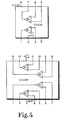
- Comparators 90-92 and 94, monostable switch 93 and flip-flop 95 may be contained in conventional integrated circuit packages. As illustrated in FIGURE 4, comparators 90 and 91 may be contained in the integrated circuit package CA393, manufactured by RCA Corporation, Somerville, New Jersey, or in the package LM393, manufactured by National Semiconductor Corporation, Santa Clara, California, with the output pins connected as indicated in FIGURES 3 and 4. Comparators 92 and 94, monostable switch 93, and flip-flop 95 may be contained by the integrated circuit package CA339, manufactured by RCA Corporation, or from the package LM339, manufactured by National Semiconductor Corporation.
Claims (15)
Priority Applications (1)
| Application Number | Priority Date | Filing Date | Title |
|---|---|---|---|
| AT80304277T ATE7639T1 (de) | 1979-11-30 | 1980-11-27 | Geregelte ablenkschaltung mit anlaufsteuerung. |
Applications Claiming Priority (4)
| Application Number | Priority Date | Filing Date | Title |
|---|---|---|---|
| GB7941461 | 1979-11-30 | ||
| GB7941461 | 1979-11-30 | ||
| US06/167,996 US4291257A (en) | 1979-11-30 | 1980-07-14 | Regulated deflection circuit with start-up and electronic circuit breaker control |
| US167996 | 2002-06-12 |
Publications (2)
| Publication Number | Publication Date |
|---|---|
| EP0030136A1 EP0030136A1 (de) | 1981-06-10 |
| EP0030136B1 true EP0030136B1 (de) | 1984-05-23 |
Family
ID=26273752
Family Applications (1)
| Application Number | Title | Priority Date | Filing Date |
|---|---|---|---|
| EP19800304277 Expired EP0030136B1 (de) | 1979-11-30 | 1980-11-27 | Geregelte Ablenkschaltung mit Anlaufsteuerung |
Country Status (4)
| Country | Link |
|---|---|
| EP (1) | EP0030136B1 (de) |
| DE (1) | DE3067972D1 (de) |
| ES (1) | ES497267A0 (de) |
| FI (1) | FI74854C (de) |
Families Citing this family (2)
| Publication number | Priority date | Publication date | Assignee | Title |
|---|---|---|---|---|
| CA1191545A (en) * | 1981-10-30 | 1985-08-06 | George R. Rusk | Power source circuit |
| CN110392469B (zh) * | 2019-07-18 | 2022-03-08 | 上海外高桥造船有限公司 | 船舶led照明系统及其软启动装置 |
Family Cites Families (5)
| Publication number | Priority date | Publication date | Assignee | Title |
|---|---|---|---|---|
| GB1481518A (en) * | 1973-10-23 | 1977-08-03 | Rca Corp | Power supply and line deflection circuit for television receivers |
| US4112465A (en) * | 1977-08-22 | 1978-09-05 | Rca Corporation | Thrush current start-up circuit for a television receiver including a start-up decoupling circuit |
| US4146823A (en) * | 1978-01-20 | 1979-03-27 | Rca Corporation | Regulated deflection circuit |
| US4147964A (en) * | 1978-02-09 | 1979-04-03 | Rca Corporation | Complementary latching disabling circuit |
| US4232254A (en) * | 1978-11-29 | 1980-11-04 | Rca Corporation | Regulated deflection circuit |
-
1980
- 1980-11-21 FI FI803633A patent/FI74854C/fi not_active IP Right Cessation
- 1980-11-27 DE DE8080304277T patent/DE3067972D1/de not_active Expired
- 1980-11-27 EP EP19800304277 patent/EP0030136B1/de not_active Expired
- 1980-11-28 ES ES497267A patent/ES497267A0/es active Granted
Also Published As
| Publication number | Publication date |
|---|---|
| FI74854B (fi) | 1987-11-30 |
| FI74854C (fi) | 1988-03-10 |
| FI803633L (fi) | 1981-05-31 |
| EP0030136A1 (de) | 1981-06-10 |
| ES8106634A1 (es) | 1981-08-16 |
| DE3067972D1 (en) | 1984-06-28 |
| ES497267A0 (es) | 1981-08-16 |
Similar Documents
| Publication | Publication Date | Title |
|---|---|---|
| KR0163762B1 (ko) | 스위치 모드 전원 장치 | |
| JP4460105B2 (ja) | ソフトスイッチングレギュレータ型電源装置及びその出力調整方法 | |
| US5270823A (en) | Run/standby control with switched mode power supply | |
| US4282460A (en) | Deflection and power supply circuit with reduced start-up drive | |
| US4385263A (en) | Television receiver, push-pull inverter, ferroresonant transformer power supply synchronized with horizontal deflection | |
| US4466051A (en) | Regulated power supply incorporating a power transformer having a tightly coupled supplemental power transfer winding | |
| US5013980A (en) | Voltage regulator in a television apparatus | |
| US4146823A (en) | Regulated deflection circuit | |
| EP0386989B1 (de) | Schaltnetzteil mit Burst-Mode-Bereitschaftsbetrieb | |
| EP0332095B1 (de) | Schaltnetzteil | |
| US4930060A (en) | Switch-mode power supply | |
| EP0030136B1 (de) | Geregelte Ablenkschaltung mit Anlaufsteuerung | |
| US4227125A (en) | Regulated deflection system | |
| US4301394A (en) | Horizontal deflection circuit and power supply with regulation by horizontal output transistor turn-off delay control | |
| US4291257A (en) | Regulated deflection circuit with start-up and electronic circuit breaker control | |
| US4484113A (en) | Regulated deflection circuit | |
| US5032967A (en) | SMPS apparatus having a demagnetization circuit | |
| JPH02273073A (ja) | スイッチモード電源 | |
| JPS63232584A (ja) | 待機モードにおけるチョップ式電源の制御回路 | |
| CA1292560C (en) | High voltage regulator in a television apparatus | |
| US3914653A (en) | Voltage regulator for deflection circuit | |
| GB2032658A (en) | Regulated deflection system e.g. for television receivers | |
| US4214189A (en) | Regulated deflection circuit | |
| EP0158492B1 (de) | Zeilenablenkungsschaltung mit Rasterverzerrungskorrektur | |
| EP0204369B1 (de) | Ablenkungsschaltung |
Legal Events
| Date | Code | Title | Description |
|---|---|---|---|
| PUAI | Public reference made under article 153(3) epc to a published international application that has entered the european phase |
Free format text: ORIGINAL CODE: 0009012 |
|
| AK | Designated contracting states |
Designated state(s): AT DE FR GB IT |
|
| 17P | Request for examination filed |
Effective date: 19820113 |
|
| ITF | It: translation for a ep patent filed |
Owner name: ING. C. GREGORJ S.P.A. |
|
| GRAA | (expected) grant |
Free format text: ORIGINAL CODE: 0009210 |
|
| AK | Designated contracting states |
Designated state(s): AT DE FR GB IT |
|
| REF | Corresponds to: |
Ref document number: 7639 Country of ref document: AT Date of ref document: 19840615 Kind code of ref document: T |
|
| REF | Corresponds to: |
Ref document number: 3067972 Country of ref document: DE Date of ref document: 19840628 |
|
| ET | Fr: translation filed | ||
| PLBE | No opposition filed within time limit |
Free format text: ORIGINAL CODE: 0009261 |
|
| STAA | Information on the status of an ep patent application or granted ep patent |
Free format text: STATUS: NO OPPOSITION FILED WITHIN TIME LIMIT |
|
| 26N | No opposition filed | ||
| ITPR | It: changes in ownership of a european patent |
Owner name: CESSIONE;RCA LICENSING CORPORATION |
|
| REG | Reference to a national code |
Ref country code: FR Ref legal event code: TP |
|
| REG | Reference to a national code |
Ref country code: GB Ref legal event code: 732 |
|
| ITTA | It: last paid annual fee | ||
| PGFP | Annual fee paid to national office [announced via postgrant information from national office to epo] |
Ref country code: AT Payment date: 19951009 Year of fee payment: 16 |
|
| PG25 | Lapsed in a contracting state [announced via postgrant information from national office to epo] |
Ref country code: AT Effective date: 19961127 |
|
| PGFP | Annual fee paid to national office [announced via postgrant information from national office to epo] |
Ref country code: DE Payment date: 19971002 Year of fee payment: 18 |
|
| PGFP | Annual fee paid to national office [announced via postgrant information from national office to epo] |
Ref country code: GB Payment date: 19971006 Year of fee payment: 18 |
|
| PGFP | Annual fee paid to national office [announced via postgrant information from national office to epo] |
Ref country code: FR Payment date: 19971007 Year of fee payment: 18 |
|
| PG25 | Lapsed in a contracting state [announced via postgrant information from national office to epo] |
Ref country code: GB Free format text: LAPSE BECAUSE OF NON-PAYMENT OF DUE FEES Effective date: 19981127 |
|
| GBPC | Gb: european patent ceased through non-payment of renewal fee |
Effective date: 19981127 |
|
| PG25 | Lapsed in a contracting state [announced via postgrant information from national office to epo] |
Ref country code: FR Free format text: LAPSE BECAUSE OF NON-PAYMENT OF DUE FEES Effective date: 19990730 |
|
| REG | Reference to a national code |
Ref country code: FR Ref legal event code: ST |
|
| PG25 | Lapsed in a contracting state [announced via postgrant information from national office to epo] |
Ref country code: DE Free format text: LAPSE BECAUSE OF NON-PAYMENT OF DUE FEES Effective date: 19990901 |