EP0023599A2 - Soldering clip for microsoldering joints - Google Patents
Soldering clip for microsoldering joints Download PDFInfo
- Publication number
- EP0023599A2 EP0023599A2 EP80103935A EP80103935A EP0023599A2 EP 0023599 A2 EP0023599 A2 EP 0023599A2 EP 80103935 A EP80103935 A EP 80103935A EP 80103935 A EP80103935 A EP 80103935A EP 0023599 A2 EP0023599 A2 EP 0023599A2
- Authority
- EP
- European Patent Office
- Prior art keywords
- thermode
- soldering
- hold
- down device
- soldered
- Prior art date
- Legal status (The legal status is an assumption and is not a legal conclusion. Google has not performed a legal analysis and makes no representation as to the accuracy of the status listed.)
- Withdrawn
Links
Images
Classifications
-
- B—PERFORMING OPERATIONS; TRANSPORTING
- B23—MACHINE TOOLS; METAL-WORKING NOT OTHERWISE PROVIDED FOR
- B23K—SOLDERING OR UNSOLDERING; WELDING; CLADDING OR PLATING BY SOLDERING OR WELDING; CUTTING BY APPLYING HEAT LOCALLY, e.g. FLAME CUTTING; WORKING BY LASER BEAM
- B23K3/00—Tools, devices, or special appurtenances for soldering, e.g. brazing, or unsoldering, not specially adapted for particular methods
- B23K3/04—Heating appliances
- B23K3/047—Heating appliances electric
- B23K3/0471—Heating appliances electric using resistance rod or bar, e.g. carbon silica
-
- H—ELECTRICITY
- H05—ELECTRIC TECHNIQUES NOT OTHERWISE PROVIDED FOR
- H05K—PRINTED CIRCUITS; CASINGS OR CONSTRUCTIONAL DETAILS OF ELECTRIC APPARATUS; MANUFACTURE OF ASSEMBLAGES OF ELECTRICAL COMPONENTS
- H05K3/00—Apparatus or processes for manufacturing printed circuits
- H05K3/30—Assembling printed circuits with electric components, e.g. with resistor
- H05K3/32—Assembling printed circuits with electric components, e.g. with resistor electrically connecting electric components or wires to printed circuits
- H05K3/34—Assembling printed circuits with electric components, e.g. with resistor electrically connecting electric components or wires to printed circuits by soldering
- H05K3/341—Surface mounted components
- H05K3/3421—Leaded components
-
- H—ELECTRICITY
- H05—ELECTRIC TECHNIQUES NOT OTHERWISE PROVIDED FOR
- H05K—PRINTED CIRCUITS; CASINGS OR CONSTRUCTIONAL DETAILS OF ELECTRIC APPARATUS; MANUFACTURE OF ASSEMBLAGES OF ELECTRICAL COMPONENTS
- H05K3/00—Apparatus or processes for manufacturing printed circuits
- H05K3/30—Assembling printed circuits with electric components, e.g. with resistor
- H05K3/32—Assembling printed circuits with electric components, e.g. with resistor electrically connecting electric components or wires to printed circuits
- H05K3/34—Assembling printed circuits with electric components, e.g. with resistor electrically connecting electric components or wires to printed circuits by soldering
- H05K3/3494—Heating methods for reflowing of solder
Definitions
- the present invention relates to a soldering iron with resistance heating for micro solder joints, in particular for the installation of micropacks in printed circuits (printed circuit boards) and in layer circuits in thick-film and thin-film technology, consisting of a frame-shaped thermode which is guided on both sides by electrodes and to the electrical power supply connected.
- soldering stamp In DE-OS 28 18 958 a soldering stamp is described and shown, on which a soldering surface with a substantially rectangular configuration is arranged via a mechanical and galvanic connection. This soldering stamp cannot be used for the installation of micropacks because it does not guarantee that the connections will rest on the circuit during the soldering process.
- the invention has for its object to implement the above-mentioned soldering iron with the simplest possible means so that it is also completely for the installation of Micropacks in printed circuits (printed circuit boards) can be used.
- This object is achieved in that the frame thermometer encloses a spring-loaded hold-down device, which contains a clearance for the solder joint, in particular for a chip, and that the frame thermode rests in the soldered state either on the connections of the substrate or on the connection ends of the component to be soldered. In this way it is ensured that the connections are all pressed on during the soldering process and thereby reliable soldering is achieved, in particular also for components with many connections. This is supported by the fact that when the hold-down device cools down until the solder joints solidify, it presses against the ends of the connections of the component.
- the hold-down device is provided with a vacuum feed and also serves as suction forceps.
- Working with the soldering clip can also be automated with the help of additional control elements.
- the hold-down device has a double function, namely the pressing of the connections and the tweezers.
- the hold-down device has a double function, namely the pressing of the connections and the tweezers.
- the hold-down device transported from a supply roll via a drive a micropack to a trimmer and after separation by means of the vacuum suction of the hold-down. Then the soldering iron with the micropack moves into the installation position.
- the circuit board to be assembled is positioned using an x-y table so that the micropack can be lowered and soldered.
- the hold-down device and the thermode can be moved in the z-direction, so that the hold-down device designed as suction tweezers is arranged on the front of the object to be soldered and the electrodes with the thermode are arranged on the back are.
- the hold-down device designed as suction tweezers is arranged on the front of the object to be soldered and the electrodes with the thermode are arranged on the back are.
- thermode In the context of the invention, the temperature of the thermode is also regulated via a thermocouple.
- thermode In order to avoid damage to sensitive semiconductor components due to the alternating voltage drop at the thermode, the thermode can be coated with an insulating layer, e.g. B. A1 2 0 3 can be provided.
- an insulating layer e.g. B. A1 2 0 3 can be provided.
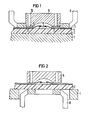
- a printed circuit board 2 is located on a support 1, on which a chip 3 rests in the middle as shown in the figure. 4 denotes a conductor track visible at the interface and 5 the associated solder layer. Terminal lugs 6 lead from the chip 3 to a polyimide carrier 7. A thermode 8 surrounds a hold-down device 9 in which bores 10 are provided. The intended solder connections are designated by 11.
- the isolated micropack 3, 6 and 7 is opened with the tweezers in the form of the hold-down device 9 take, positioned on the slot on the circuit board 2 and placed.
- the frame-shaped thermode 8 is then lowered onto the circuit outside the micropack, so that the heat for the soldering process reaches the connection points via the soldered conductor tracks.
- the micropack is held down until the solder has solidified without tension. Thereafter, thermode 8 and hold-down device 9 are lifted off.
- the structure of the soldering iron is changed such that the hold-down device 9 designed as tweezers and the thermode 8 are arranged on the back of the circuit.
- the hold-down device and thermode are designed to be movable in the Z direction.
- the circuit board 2 is the ceramic carrier for a thick-film or thin-film circuit.
Abstract
Description
Die vorliegende Erfindung betrifft einen Lötbügel mit Widerstandsheizung für Mikrolötstellen, insbesondere für den Einbau von Mikropacks in gedruckten Schaltungen (Leiterplatten) und in Schichtschaltungen in Dickschicht-und Dünnfilmtechnik, bestehend aus einer rahmenförmigen Thermode, die an beiden Seiten von Elektroden geführt und an die elektrische Stromversorgung angeschlossen ist.The present invention relates to a soldering iron with resistance heating for micro solder joints, in particular for the installation of micropacks in printed circuits (printed circuit boards) and in layer circuits in thick-film and thin-film technology, consisting of a frame-shaped thermode which is guided on both sides by electrodes and to the electrical power supply connected.
In der DE-OS 28 18 958 ist ein Lötstempel beschrieben und dargestellt, an welchem über eine mechanische und galvanische Verbindung eine Lötfläche mit im wesentlichen rechteckiger Ausbildung angeordnet ist. Dieser Lötstempel ist für den Einbau von Mikropacks nicht anwendbar, weil damit nicht gewährleistet ist, daß die Anschlüsse beim Lötvorgang auf der Schaltung aufliegen.In DE-OS 28 18 958 a soldering stamp is described and shown, on which a soldering surface with a substantially rectangular configuration is arranged via a mechanical and galvanic connection. This soldering stamp cannot be used for the installation of micropacks because it does not guarantee that the connections will rest on the circuit during the soldering process.
Der Erfindung liegt die Aufgabe zugrunde, den eingangs genannten Lötbügel mit möglichst einfachen Mitteln so zu realisieren, daß er vollständig auch für den Einbau von Mikropacks in gedruckten Schaltungen (Leiterplatten) anwendbar ist. Diese Aufgabe wird dadurch gelöst, daß die Rahmenthermode einen gefederten Niederhalter umschließt, der eine Freinehmung für die Lötstelle, insbesondere für einen Chip, enthält und daß die Rahmenthermode im Lötzustand entweder auf den Anschlüssen des Substrates bzw. auf den Anschlußenden des zu lötenden Bauteiles aufliegt. Auf diese Weise wird gewährleistet, daß-die Anschlüsse beim Lötprozeß alle angedrückt werden und dadurch eine sichere Lötung insbesondere auch bei Bauelementen mit vielen Anschlüssen erzielt wird. Unterstützend kommt hinzu, daß beim Abkühlen der Niederhalter bis zum Erstarren der Lotstellen gegen die Enden der Anschlüsse des Bauelementes drückt.The invention has for its object to implement the above-mentioned soldering iron with the simplest possible means so that it is also completely for the installation of Micropacks in printed circuits (printed circuit boards) can be used. This object is achieved in that the frame thermometer encloses a spring-loaded hold-down device, which contains a clearance for the solder joint, in particular for a chip, and that the frame thermode rests in the soldered state either on the connections of the substrate or on the connection ends of the component to be soldered. In this way it is ensured that the connections are all pressed on during the soldering process and thereby reliable soldering is achieved, in particular also for components with many connections. This is supported by the fact that when the hold-down device cools down until the solder joints solidify, it presses against the ends of the connections of the component.
Nach einer Weiterbildung der Erfindung ist der Niederhalter mit einer Vakuumzuführung versehen und dient zugleich als Saugpinzette. Das Arbeiten mit dem Lötbügel kann mit Hilfe zusätzlicher Steuerglieder auch automatisiert werden. In diesem Zusammenhang hat der Niederhalter dann eine Doppelfunktion, und zwar das Andrücken der Anschlüsse und der Saugpinzette. Hierbei wird z. B. von einer Vorratsrolle über einen Antrieb jeweils ein Mikropack zu einer Beschneidevorrichtung transportiert und nach dem Abtrennen mit Hilfe der Vakuumansaugung des Niederhalters aufgenommen. Anschließend fährt dann der Lötbügel mit dem Mikropack in die Einbauposition. Dabei wird z. B. die zu bestückende Leiterplatte mit Hilfe eines x-y-Tisches positioniert, so daß das Mikropack abgesenkt und eingelötet werden kann.According to a development of the invention, the hold-down device is provided with a vacuum feed and also serves as suction forceps. Working with the soldering clip can also be automated with the help of additional control elements. In this context, the hold-down device has a double function, namely the pressing of the connections and the tweezers. Here, for. B. transported from a supply roll via a drive a micropack to a trimmer and after separation by means of the vacuum suction of the hold-down. Then the soldering iron with the micropack moves into the installation position. Here, for. B. the circuit board to be assembled is positioned using an x-y table so that the micropack can be lowered and soldered.
Nach einer weiteren Ausgestaltung der Erfindung ist der Niederhalter und die Thermode in z-Richtung verfahrbar, so daß an der Vorderseite des zu lötenden Gegenstandes der als Saugpinzette ausgebildete Niederhalter und an der Rückseite die Elektroden mit der Thermode angeordnet sind. Auf diese Weise wird erreicht, daß mit der Impulsbeheizten Thermode die Wärmezufuhr von der Schaltungsrückseite möglich wird, wenn infolge hoher Packungsdichte kein Freiraum auf der Schaltung für die Thermode vorgesehen werden kann.According to a further embodiment of the invention, the hold-down device and the thermode can be moved in the z-direction, so that the hold-down device designed as suction tweezers is arranged on the front of the object to be soldered and the electrodes with the thermode are arranged on the back are. In this way it is achieved that with the pulse-heated thermode the supply of heat from the back of the circuit becomes possible if, owing to the high packing density, no space can be provided on the circuit for the thermode.
Im Rahmen der Erfindung wird ferner die Temperatur der Thermode über ein Thermoelement geregelt.In the context of the invention, the temperature of the thermode is also regulated via a thermocouple.
Um bei empfindlichen Halbleiterbauelementen eine Beschädigung durch den Wechselspannungsabfall an der Thermode zu vermeiden, kann die Thermode mit einer Isolierschicht, z. B. A1203, versehen werden.In order to avoid damage to sensitive semiconductor components due to the alternating voltage drop at the thermode, the thermode can be coated with an insulating layer, e.g. B. A1 2 0 3 can be provided.
Die Erfindung wird anhand der Figuren erläutert. Es zeigen:
- Figur 1 einezLötbügel, bei dem Thermode und Niederhalter auf derselben Seite der Schaltung angeordnet sind und
Figur 2 einen Lötbügel, bei dem auf der Vorderseite der Niederhalter und auf der Schaltungsrückseite die Thermode angeordnet ist.
- Figure 1 a soldering clip in which the thermode and hold-down device are arranged on the same side of the circuit and
- Figure 2 shows a soldering bracket in which the thermode is arranged on the front of the hold-down device and on the back of the circuit.
Auf einer Auflage 1 befindet sich eine Leiterplatte 2, auf der nach der Darstellung in der Figur in der Mitte ein Chip 3 aufliegt. Mit 4 ist eine an der Schnittstelle sichtbare Leiterbahn und mit 5 die dazugehörige Lotschicht bezeichnet. Vom Chip 3 führen Anschlußfahnen 6 zu einem Polyimidträger 7. Eine Thermode 8 umgibt einen Niederhalter 9, in dem Bohrungen 10 vorgesehen sind. Mit 11 sind die beabsichtigten Lötverbindungen bezeichnet.A printed
Beim Einlöten wird das vereinzelte Mikropack 3, 6 und 7 mit der Saugpinzette in Form des Niederhalters 9 aufgenommen, auf den Einbauplatz auf der Leiterplatte 2 positioniert und aufgesetzt. Anschließend wird die rahmenförmige Thermode 8 außerhalb des Mikropacks auf die Schaltung abgesenkt, so daß die Wärme für den Lötprozeß über die beloteten Leiterbahnen an die Verbindungsstellen gelangt. Nach dem Aufschmelzen des beloteten Anschlußpartners zur Lötverbindung wird das Mikropack solange niedergehalten, bis das Lot spannungsfrei erstarrt ist. Danach werden Thermode 8 und Niederhalter 9 abgehoben.When soldering, the isolated micropack 3, 6 and 7 is opened with the tweezers in the form of the hold-down
Die indirekte Wärmezufuhr über die beloteten Leiterbahnen wurde deshalb angewendet, weil die Wärmezufuhr über den Polyimidträger 7, z. B. Kapton, zu Beschädigungen desselben führen könnte.The indirect supply of heat via the soldered conductor tracks was used because the supply of heat via the polyimide carrier 7, for. B. Kapton, could damage the same.
Nach der Darstellung in der Figur 2 wird der Lötbügelaufbau derart geändert, daß an der Vorderseite der als Saugpinzette ausgebildete Niederhalter 9 und an der Schaltungsrückseite die Thermode 8 angeordnet sind. Hierfür sind Niederhalter und Thermode in Z-Richtung verfahrbar ausgebildet. Bei dieser Anordnung ist die Leiterplatte 2 der Keramikträger für eine Dickschicht- oder Dünnfilmschaltung.According to the illustration in FIG. 2, the structure of the soldering iron is changed such that the hold-down
Claims (5)
Applications Claiming Priority (2)
| Application Number | Priority Date | Filing Date | Title |
|---|---|---|---|
| DE19792931857 DE2931857A1 (en) | 1979-08-06 | 1979-08-06 | SOLDERING BRACKET FOR MICROLOETING POINTS |
| DE2931857 | 1979-08-06 |
Publications (2)
| Publication Number | Publication Date |
|---|---|
| EP0023599A2 true EP0023599A2 (en) | 1981-02-11 |
| EP0023599A3 EP0023599A3 (en) | 1981-07-15 |
Family
ID=6077756
Family Applications (1)
| Application Number | Title | Priority Date | Filing Date |
|---|---|---|---|
| EP80103935A Withdrawn EP0023599A3 (en) | 1979-08-06 | 1980-07-09 | Soldering clip for microsoldering joints |
Country Status (3)
| Country | Link |
|---|---|
| EP (1) | EP0023599A3 (en) |
| JP (1) | JPS5629397A (en) |
| DE (1) | DE2931857A1 (en) |
Cited By (5)
| Publication number | Priority date | Publication date | Assignee | Title |
|---|---|---|---|---|
| US4835847A (en) * | 1988-04-20 | 1989-06-06 | International Business Machines Corp. | Method and apparatus for mounting a flexible film electronic device carrier on a substrate |
| EP0449156A1 (en) * | 1990-03-28 | 1991-10-02 | SELENIA INDUSTRIE ELETTRONICHE ASSOCIATE S.p.A. | Soldering apparatus and method employing provision of heated gas to a soldering alloy at a soldering collection |
| DE4105874C1 (en) * | 1991-02-25 | 1992-07-30 | Messerschmitt-Boelkow-Blohm Gmbh, 8012 Ottobrunn, De | |
| DE4105875C1 (en) * | 1991-02-25 | 1992-08-13 | Messerschmitt-Boelkow-Blohm Gmbh, 8012 Ottobrunn, De | |
| DE19942384A1 (en) * | 1999-09-04 | 2001-03-15 | Opel Adam Ag | Soldering device for automobile body component panels has pressure noses for pressing overlapping edges of sheet metal panels together during soldering |
Families Citing this family (2)
| Publication number | Priority date | Publication date | Assignee | Title |
|---|---|---|---|---|
| JPS57210694A (en) * | 1981-06-19 | 1982-12-24 | Hitachi Ltd | Method and device for soldering via resistance reflow |
| DE3531715A1 (en) * | 1985-09-05 | 1987-03-12 | Widmaier Fa Hans | Method and device for soldering surface-mountable components on printed circuit boards (circuit carrying boards) with track patterns |
Citations (6)
| Publication number | Priority date | Publication date | Assignee | Title |
|---|---|---|---|---|
| FR1484521A (en) * | 1965-06-24 | 1967-06-09 | Texas Instruments Inc | Device for mounting components in an electronic circuit |
| US3522407A (en) * | 1968-03-05 | 1970-08-04 | Argus Eng Co | Heating method |
| US3710481A (en) * | 1971-03-24 | 1973-01-16 | Burroughs Corp | Terminal alignment and connection device for conductors of a multiconductor cable |
| US3718800A (en) * | 1968-03-05 | 1973-02-27 | Argus Eng Co | Infrared heating apparatus |
| FR2221225A1 (en) * | 1973-03-16 | 1974-10-11 | Honeywell Bull Soc Ind | Joule effect welding tool for electronic elements - esp. for welding conductor connections to integrated circuitry |
| FR2279505A1 (en) * | 1974-07-22 | 1976-02-20 | Berco Ste Civile Etude Rech | Soldering iron tip covered with non-conductive material - preventing application of voltage to electronic components being soldered |
Family Cites Families (3)
| Publication number | Priority date | Publication date | Assignee | Title |
|---|---|---|---|---|
| US3911569A (en) * | 1974-11-18 | 1975-10-14 | Gen Motors Corp | Method and apparatus for bonding miniature semiconductor pill-type components to a circuit board |
| US3912153A (en) * | 1974-11-18 | 1975-10-14 | Gen Motors Corp | Method and apparatus for bonding semiconductor pill-type components to a circuit board |
| DE2640613C2 (en) * | 1976-09-09 | 1985-03-07 | Siemens AG, 1000 Berlin und 8000 München | Method and device for contacting circuit components in a layer circuit |
-
1979
- 1979-08-06 DE DE19792931857 patent/DE2931857A1/en not_active Ceased
-
1980
- 1980-07-09 EP EP80103935A patent/EP0023599A3/en not_active Withdrawn
- 1980-08-06 JP JP10814680A patent/JPS5629397A/en active Pending
Patent Citations (6)
| Publication number | Priority date | Publication date | Assignee | Title |
|---|---|---|---|---|
| FR1484521A (en) * | 1965-06-24 | 1967-06-09 | Texas Instruments Inc | Device for mounting components in an electronic circuit |
| US3522407A (en) * | 1968-03-05 | 1970-08-04 | Argus Eng Co | Heating method |
| US3718800A (en) * | 1968-03-05 | 1973-02-27 | Argus Eng Co | Infrared heating apparatus |
| US3710481A (en) * | 1971-03-24 | 1973-01-16 | Burroughs Corp | Terminal alignment and connection device for conductors of a multiconductor cable |
| FR2221225A1 (en) * | 1973-03-16 | 1974-10-11 | Honeywell Bull Soc Ind | Joule effect welding tool for electronic elements - esp. for welding conductor connections to integrated circuitry |
| FR2279505A1 (en) * | 1974-07-22 | 1976-02-20 | Berco Ste Civile Etude Rech | Soldering iron tip covered with non-conductive material - preventing application of voltage to electronic components being soldered |
Cited By (6)
| Publication number | Priority date | Publication date | Assignee | Title |
|---|---|---|---|---|
| US4835847A (en) * | 1988-04-20 | 1989-06-06 | International Business Machines Corp. | Method and apparatus for mounting a flexible film electronic device carrier on a substrate |
| EP0449156A1 (en) * | 1990-03-28 | 1991-10-02 | SELENIA INDUSTRIE ELETTRONICHE ASSOCIATE S.p.A. | Soldering apparatus and method employing provision of heated gas to a soldering alloy at a soldering collection |
| DE4105874C1 (en) * | 1991-02-25 | 1992-07-30 | Messerschmitt-Boelkow-Blohm Gmbh, 8012 Ottobrunn, De | |
| DE4105875C1 (en) * | 1991-02-25 | 1992-08-13 | Messerschmitt-Boelkow-Blohm Gmbh, 8012 Ottobrunn, De | |
| DE19942384A1 (en) * | 1999-09-04 | 2001-03-15 | Opel Adam Ag | Soldering device for automobile body component panels has pressure noses for pressing overlapping edges of sheet metal panels together during soldering |
| DE19942384C2 (en) * | 1999-09-04 | 2001-12-06 | Opel Adam Ag | Soldering device |
Also Published As
| Publication number | Publication date |
|---|---|
| DE2931857A1 (en) | 1981-04-16 |
| EP0023599A3 (en) | 1981-07-15 |
| JPS5629397A (en) | 1981-03-24 |
Similar Documents
| Publication | Publication Date | Title |
|---|---|---|
| EP0012319B2 (en) | Method and template for securing components having flat connecting leads onto conductive substrates | |
| EP0140126B1 (en) | Method of tape-automated bonding | |
| DE1283965B (en) | Hermetically sealed semiconductor device | |
| DE1640467B1 (en) | Process for the contact-compatible application of microminiaturized components to a dielectric base plate | |
| US4506820A (en) | Desoldering device | |
| DE19541334A1 (en) | Mfg. printed circuit assembly for construction of sub-assemblies in e.g. microwave electronic equipment | |
| NL140100B (en) | PROCEDURE FOR MANUFACTURE OF A MICROMINIATURE SWITCH FUNCTION BLOCK, INCLUDING FIXING ONE OR MORE MICROMINIATURE ELEMENTS TO A SUPPORT AND MICROMINIATURE SWITCHING FUNCTION BLOCK. | |
| EP0538280B1 (en) | Rheostatic switching arrangement | |
| DE4242408A1 (en) | Connecting liquid crystal displays to IC substrate - using patterned conducting photoresist and UV hardened resin to prevent electrodes from being short-circuited | |
| EP0464232A1 (en) | Solder connector and process for making an electrical circuit with this solder connector | |
| DE2319287A1 (en) | PROCEDURE FOR REMOVING EXCESS SOLDER FROM CONTACT FINGERS ON MODULE SUBSTRATES | |
| EP0023599A2 (en) | Soldering clip for microsoldering joints | |
| DE2640613C2 (en) | Method and device for contacting circuit components in a layer circuit | |
| US6225573B1 (en) | Method for mounting terminal on circuit board and circuit board | |
| DE4424831C2 (en) | Process for producing an electrically conductive connection | |
| DE2528000B2 (en) | Method for producing a soldering surface of relatively large dimensions | |
| DE2410849A1 (en) | Process for soldering miniature components to boards - has blobs of solder on boards contact pads re-melted to link with component | |
| JPS63276292A (en) | Method of soldering terminal of electronic component to stripe conductor of carrier and sheet carrying solder strip | |
| DE3510000A1 (en) | THERMOPLASTIC SOLDER AND METHOD AND DEVICE FOR USE THEREOF | |
| DE4117145A1 (en) | Chip mounting method on substrate - by heating adhesive layer to receiver chips from carrier | |
| DE3342279C1 (en) | Soldering method and device for carrying out the method | |
| DE3319339C2 (en) | ||
| DE4101790C1 (en) | Chip-support arrangement prodn. - in tape form, in dual-in-line format by film-bond technology | |
| DE202006020419U1 (en) | conductor structure | |
| WO1991012634A1 (en) | Process for pre-soldering a substrate |
Legal Events
| Date | Code | Title | Description |
|---|---|---|---|
| PUAI | Public reference made under article 153(3) epc to a published international application that has entered the european phase |
Free format text: ORIGINAL CODE: 0009012 |
|
| AK | Designated contracting states |
Designated state(s): CH FR IT NL |
|
| PUAL | Search report despatched |
Free format text: ORIGINAL CODE: 0009013 |
|
| AK | Designated contracting states |
Designated state(s): CH FR IT NL |
|
| 17P | Request for examination filed |
Effective date: 19811009 |
|
| STAA | Information on the status of an ep patent application or granted ep patent |
Free format text: STATUS: THE APPLICATION IS DEEMED TO BE WITHDRAWN |
|
| 18D | Application deemed to be withdrawn |
Effective date: 19830309 |
|
| RIN1 | Information on inventor provided before grant (corrected) |
Inventor name: WIRBSER, OSCAR Inventor name: UNGER, GREGOR Inventor name: MEIXNER, KARL |