EP0022866B1 - Amplitude control circuits - Google Patents
Amplitude control circuits Download PDFInfo
- Publication number
- EP0022866B1 EP0022866B1 EP79900105A EP79900105A EP0022866B1 EP 0022866 B1 EP0022866 B1 EP 0022866B1 EP 79900105 A EP79900105 A EP 79900105A EP 79900105 A EP79900105 A EP 79900105A EP 0022866 B1 EP0022866 B1 EP 0022866B1
- Authority
- EP
- European Patent Office
- Prior art keywords
- signal
- circuit
- amplifier
- resistor
- output
- Prior art date
- Legal status (The legal status is an assumption and is not a legal conclusion. Google has not performed a legal analysis and makes no representation as to the accuracy of the status listed.)
- Expired
Links
Images


Classifications
-
- H—ELECTRICITY
- H03—ELECTRONIC CIRCUITRY
- H03G—CONTROL OF AMPLIFICATION
- H03G3/00—Gain control in amplifiers or frequency changers without distortion of the input signal
- H03G3/20—Automatic control
- H03G3/30—Automatic control in amplifiers having semiconductor devices
- H03G3/3005—Automatic control in amplifiers having semiconductor devices in amplifiers suitable for low-frequencies, e.g. audio amplifiers
- H03G3/301—Automatic control in amplifiers having semiconductor devices in amplifiers suitable for low-frequencies, e.g. audio amplifiers the gain being continuously variable
-
- H—ELECTRICITY
- H03—ELECTRONIC CIRCUITRY
- H03L—AUTOMATIC CONTROL, STARTING, SYNCHRONISATION, OR STABILISATION OF GENERATORS OF ELECTRONIC OSCILLATIONS OR PULSES
- H03L5/00—Automatic control of voltage, current, or power
Definitions
- the present invention relates to an amplitude control circuit suitable for stabilizing the oscillation output level of a sine wave oscillator and also suitable for dynamically controlling the signal output level of an automatic level control (ALC) circuit.
- ALC automatic level control
- an amplitude control circuit of oscillators or ALC circuits the level or amplitude change of an output or an input signal must be quickly detected. Namely, a quick response characteristic is required for a control circuit of sine wave oscillators or ALC circuits.
- the time constant of a ripple filter provided in the control signal circuit path has to be as small as possible.
- a small time constant increases ripples of the control signal, resulting in high distortion factor. Accordingly, the quick response and the low distortion factor are contradictory to each other.
- an amplitude control circuit for analog signals comprising:
- said control signal means includes rectifying means and filter means having defined charge/discharge time constants for further reducing ripple components of said ' control signal (e 4 ) which corresponds to the amplitude of said input signal (ei), which is characterized in that one of the defined charge/ discharge time constants of said filter means at the time when the amplitude of said input signal (ei) increases is smaller than the other of said charge/discharge time constants of said filter means at the time when the amplitude of said input signal (ei) decreases.
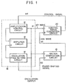
- Fig. 1 shows a basic configuration of sine-wave oscillator which includes an amplitude control circuit according to the invention.
- An output . signal e1 of an amplifier circuit 10 is input to an amplification control circuit 12.
- the signal e1 is positively (or negatively) fed back to a first input of the amplifier 10 through the control circuit 12.
- the signal e1 is negatively (or positively) fed back to a second input of the amplifier 10 via an oscillation frequency setting circuit 14.
- the circuit components 10, 12 and 14 constitute a conventional oscillation circuit 16.
- the signals supplied to the first and second input of the amplifier 10 are, e.g., positive and negative feedback signals, respectively.
- the oscillation circuit 16 forms Sulzer type (Bridged T type) oscillator.
- the oscillation circuit 16 forms Wienbridge type oscillator.
- the signal e1 is supplied to a first input of a vector composition circuit 18.
- a second input of the composition circuit 18 is supplied with a phase-shifted signal e2 which is derived from the setting circuit 14.
- a phase-shift amount about 45° of the signal e2 as against the signal e1 can be obtained.
- the signals e1 and e2 are converted into a signal e3 whose phase is shifted by 90° from the signal e1, by means of the composition circuit 18. For example, when the signal e1 is a sine-wave, the signal e3 is a cosine-wave.
- the signal e1 is supplied to a first input of a control signal generation circuit 20.
- a second input of the generation circuit 20 is supplied with the signal e3.
- the control signal generation circuit 20 synthesizes a control signal e4 which includes a DC component proportional to the sum of squared signals e1 and e3. That is, the DC component of the signal e4 can be explained by a function with parameter of e1 2 +e3 2 .
- the signals e1 and e3 are defined as below: wherein E denotes an amplitude (corresponding to the peak value) of each signals e1 and e3, w an angular frequency and t a time.
- the signal e4 is expressed as wherein k denotes a proportion constant which is a property of the generation circuit 20.
- the signal e4 is independent of the angular frequency ⁇ of the oscillation output signal e1.
- the signal e4 only contains information proportional to the square of amplitude E of the signal e1.
- the transfer function of the control circuit 12 is controlled.
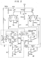
- Fig. 2 is a detail circuit diagram of the basic configuration shown in Fig. 1. The inventor believes that this circuit configuration is a best mode at the time the application is filed.
- An output of an amplifier 10 is connnected via a resistor R12 2 to a non-inverted input of the amplifier 10.
- the non-inverted input is grounded through a resistance R12, of an impedance controlled element 12 1 .
- a photo-coupler combining LED and CdS cell is preferably applied.
- the element 12, and the resistor R12 2 form the amplification control circuit 12.
- An inverted input of the amplifier 10 is connected to the output thereof, through a resistor R14 1 .
- a series circuit of capacitors C14, and C14 2 is parallel connected to the resistor R14 1 .
- the connection point of capacitors C14, and C14 2 is connected via a resistor R14 2 to an inverted input of an amplifier 22.
- the resistors R14 1 , R14 2 and the capacitors C14 1 , C14 2 form the oscillation frequency setting circuit 14 of Bridged Ttype.
- the amplifier 10, impedance controlled element 12 1 , resistors R12 2 , R14 1 , R14 2 and capacitors C14,, C14 2 constitute the oscillation circuit 16.
- the inverted input of the amplifier 22 is connected to an output thereof via a resistor R18 1 .
- a non-inverted input of the amplifier 22 is grounded through a resistor R18 2 .
- the resistor R18 2 is provided for an off-set balancing.
- the output of the amplifier 22 is connected to the output of the amplifier 10 through a series circuit of resistors R18 3 and R18 4 .
- the amplifier 22 and the resistors R18, to R18 4 form the vector composition circuit 18.
- the inverted input of the amplifier 22 is in the state of "imaginary ground”. That is, the junction point of the resistors R14 2 and R18 1 is equivalently grounded. At the connection point of the capacitor C14, and C14 2 in the oscillation frequency setting circuit 14, the phase-shifted signal e2 appears.
- the phase-shifted signal e2 is a sine-wave voltage signal having a phase difference ⁇ from the sine-wave oscillation output signal e1 of the oscillation circuit 16.
- the signal e2 is converted to a current signal i2 corresponding to e2/R14 2 and input to the vector composition circuit 18.
- the current signal i 2 is converted into a phase-shifted signal e2a by the amplifier 22.
- the phase-shifted signal e2a is antiphased from the signal e2.
- the amplitude of the signal e2 a can be varied by the resistor R18 1 .
- the phase-shifted signal e2a and the oscillation output signal e1 are added by an adder circuit being formed of the resistors R18 3 and R18 4 . By this addition a phase-shifted signal e3 whose phase is differenced by 90° from the signal e1, is obtained.
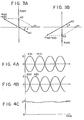
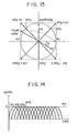
- Fig. 3A This figure illustrates how the composition of the phase-shifted signal e3 is performed in the vector composition circuit 18.
- the phase-shifted signal e2 is phase-delayed by ⁇ from the oscillation output signal e1.
- the phase-shifted signal e2a is obtained.
- a phase-shifted signal e3 is composed.
- the phase difference between the signal e1 and the signal e3 can be set at 90° by adjusting the amplitude rate A i .
- the vector composition circuit 18 composes a cosine-wave signal from a sine-wave signal.
- a 90° phase-shifted signal A z e3 whose amplitude is equal to the oscillation output signal e1, is obtained from amplifying the signal e3 by A 2 .
- Fig. 2 in which the output of the amplifier 10 is connected to an inverted input of an amplifier 24, through a series circuit of resistors R20 1 and R20 2 .
- the inverted input of the amplifier 24 is coupled with its output via a resistor R20 3 .
- a non-inverted input of the amplifier 24 is grounded by way of a resistor R20 4 for off-set balancing.
- the junction point of the resistors R18 3 and R18 4 is connected to an inverted input of an amplifier 26, through a series circuit of resistors R20 5 and R20 6 .
- the inverted input of the amplifier 26 is coupled with its output via a resistor R20 7 .
- a non-inverted input of the amplifier 26 is grounded by way of a resistor R20 8 .
- phase difference of 90° is presented between the signals e1a and e3a.
- Amplitudes of the signals e1a a and e3a can be adjusted by the resistors R20, and R20 5 , respectively.
- the amplitudes of signals e1a and e3a can therefore be set to equal each other.
- the phase relations of the signals e1a, -e1a and the signals e3a, -e3a are respectively shown in Figs. 4A and 4B.
- the junction point of the resistors R20 1 and R20 2 is connected to the gate of a P channel MOS FET 28.
- the output of the amplifier 24 is connected to the gate of a P channel MOS FET 30.
- the junction point of R20 5 and R20 6 and the output of the amplifier 26 are connected to the gates of P channel MOS FETs 32 and 34, respectively.
- an enhancement type is used for the FETs 28 to 34.
- any type of device may be used whose characteristic of drain current I D can substantially be represented by a square-function of its gate-source voltage V GS .
- a depletion type may be applied to FETs 28 to 34.
- Fig. 5 shows a typical I D -V GS characteristic of P channel FET.
- a curve "A” indicates an enhancement type and -V TH designates its threshold voltage.
- a curve “B” indicates a depletion type and +Vp designates its pinch-off voltage.
- the curves "A”, "B” can be represented by a square-function with good accuracy.
- the drains of FETs 28 and 30 are connected through a resistor R20 9 to a negative power source -V E .
- the drains of FETs 32 and 34 are connected to the power source -V E via a resistor R20 10 .
- the resistors R20 9 and R20 10 are used for over-current limiter.
- Each substrate and source of FETs 28 and 30 is connected to the emitter of an NPN transistor 36.
- each substrate and source of FETs 32 and 34 is connected to the emitter of an NPN transistor 38.
- the bases of the transistors 36 and 38 are connected to the base and collector of an NPN transistor 40.
- the emitter of the transistor 40 is grounded through a resistor R20 11 .
- the collector of the transistor 40 is connected to a positive power source +V c via a resistor R20 12 .
- the diode-connected transistor 40 is provided for temperature-compensation of the base-emitter threshold voltages V BE of the transistors 36 and 38.
- Gate bias voltages V GS for the FETs 28 to 34 can be adjusted by the resistor R20 12 .
- "dual" type in which electrical characteristics of packed pellets are matched, are suitable for the FETs 28 and 30, also for the FETs 32 and 34.
- the collectors of the transistors 36 and 38 are connected through a resistor R20 13 to the cathode of an LED or light emission device which is coupled with the impedance controlled element 12 1 .
- the anode of the LED is connected to the positive power source +V c .
- the collectors of the transistors 36 and 38 are grounded, via a capacitor C20 1 .
- the capacitor C20 is provided for decreasing remaining ripples included in a control current 1 4 or in a control voltage e4 which is applied to the amplification control circuit 12. If the I D- V GS characteristics of the FETs 28 to 34 may completely be regarded as a square function, the control current I 4 does not involve the ripples.
- the current I 4 includes some ripples. Frequency components of the ripple are higher harmonics over second order of the oscillation output signal e1's frequency. Moreover the amplitude of the ripple component is extremely small as compared with the DC level of the control current I4. The time constant may therefore be small, which is formed of the capacitor C20 1 and the corrector circuit impedance of the transistors 36 and 38.
- the amplifiers 24 and 26 , FETs 28 to 34, transistors 36 to 40, resistors R20 1 to R20 13 and the capacitor C20, are constituting the control signal generation circuit 20.
- the composing operation of the control current 1 4 i.e. the control signal e4 as set forth in equation (3), can be explained as described below. This explanation will be made by referring Figs. 4 and 5.
- the source-potentials of FETs 28 to 34 are adjusted at the threshold voltage +V TH .
- the gate voltage -V GS to the sources of FETs 28, 30 or FETs 32,34 are ⁇ V TH at the time of zero-amplitude of the signal e1 a or e3a.
- the FET 28 is cut-off during the positive half period of the signal e1a.
- a current i 28 proportional to e1a 2 is flowing into the source-drain path of FET 28.
- a current i 30 proportional to (-e1 a) 2 is flowing into the FET 30.
- a current i 28 +i 30 proportional to e1a 2 flows in the collector circuit of the transistor 36 along the whole phase.
- a current i 32 proportional to e3a z and a current i 34 to (-e3a) 2 are flowing into the FETs 32 and 34, respectively.
- a current i 32 +i 34 proportional to e3a z flows in the collector circuit of the transistor 38 along the whole phase.
- the sum of the currents i z8 , i 30 , i 32 and i 34 provides the control current I4.
- a collector voltage e4a of the transistors 36 and 38 corresponding to the control current 1 4 is a DC signal including some ripples, as shown in Fig. 4C. The ripples will appear when said square-function characteristics can not precisely be obtained.
- the level of the DC signal is proportional to the square of the amplitude of oscillation output signal e1, but has no relation to the oscillation frequency.
- the control current 1 4 also has a waveform as shown in Fig. 4C. By using such control current 1 4 , a CR oscillator with low-distortion and low-hunting can be provided.
- a stable oscillation output signal can be obtained irrespective of its oscillation frequency. Accordingly, an extreme low frequency sine-wave signal, which has only been put to practical use by a function generator, can be obtained by a conventional Sulzer type or Wien-bridge type oscillator circuit with this invention.
- a function generator is widely used for an extremely low frequency band sine-wave oscillator.
- Accurate conversion of this function is difficult, technically. It is therefore hard to obtain a low distortion sine-wave from a triangle-wave. Further, a sine-wave obtained from this functional conversion is attended with a large distortion including much higher harmonics of odd number order.
- Fig. 2 an extremely low frequency sine-wave signal e1 with low distortion factor can be obtained.
- Fig. 6 shows a modification of oscillation circuit 16 applicable to this invention.
- a bootstrap type positive feedback circuit is applied to the oscillation frequency setting circuit 14.
- This positive feedback circuit is one modification of another Japanese Patent Application "Band Rejection Circuit" which is made by the same inventor.
- This application is Japanese Patent Application No. 145981/76 filed on December 4, 1976 and is amended on August 23, 1977.
- a positive feedback circuit of the amplifier 10 or the amplification control circuit 12 has the same configuration of Fig. 2.
- the negative feedback circuit is constructed as below.
- the output of the amplifier 10 is connected to a non-inverted input of an amplifier 14 1 , via a series circuit of resistors R14, and R14 2 .
- the junction point of the resistors R14, and R14 2 is connected through a capacitor C14, to an output of the amplifier 14 1 .
- the output of the amplifier 14, is connected through a resistor R14 4 to an inverted input thereof.
- the inverted input of the amplifier 14, is grounded via a resistor R14 5 .
- the non-inverted input of the amplifier 14, is connected through a capacitor C14 2 to the non-inverted input of the amplifier 10.
- the non-inverted input of the amplifier 10 is grounded via a resistor R14 3 .
- a device for varying the oscillation frequency may be single. This means that such a circuit is particularly suitable to constitute a voltage controlled oscillator (VCO).
- VCO voltage controlled oscillator
- an oscillation circuit of Sulzer or Wien-bridge type at least a two-ganged or more ganged type variable resistor or variable capacitor (variable condenser) is required for varying the oscillation frequency, and when such a ganged device includes a gang-error the amplitude of the oscillation output e1 is liable to vary with varying the oscillation frequency.
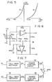
- Fig. 7 shows a modification of the square function composition circuit in the control signal generation circuit 20.
- a square function characteristic between the gate-source voltage V GS and the drain current I D of FETs 28-34 is applied.
- a full-wave rectification for the signals e1 and e2 is realized by the FETs 28 to 34 such that these FETs are cut-off during the positive half period of ⁇ e1 and ⁇ e3.
- Such a full-wave rectification and square function composition of the FETs 28 to 34 may be realized by a general configuration as shown in Fig. 7.
- the signal e1 is converted to, for example, a pulsation signal e1a of positive period of sine-wave by a full-wave rectifier 70.
- the signal e1a is converted to a squared signal e1a 2 by a square function circuit 72.
- the signal e3 is converted to a squared signal e3a z through a full-wave rectifier 74 and a square function circuit 76.
- the squared signals e1a 2 and e3a 2 is added by an adder 78. Then the adder 78 provides the squared signal
- the full-wave rectifiers 70, 74 and the square function circuit 72, 76 and the adder 78 may be conventional ones.
- a linear rectifier circuit which comprises an operational amplifier whose negative feedback loop includes a rectifying diode or a rectifying transistor, is suitable.
- the square function circuit 72 or 76 following circuit means is suitable.
- An output of an amplifier 72 is connected to the drain of an N channel depletion type FET 72 2 .
- the source of the FET 72 2 is connected to an inverted input of the amplifier 72 1 .
- the inverted input is grounded via a resistor R72 1 .
- Connected between the source and gate of the FET is a gate-bias voltage source 72 3 .
- the curve of the drain current and source-drain voltage of the FET 72 2 can be varied by changing the voltage of the source 72 3 .
- Figs. 9 through 12 show modifications of the oscillation circuit 16 shown in Fig. 2.
- a resistor R12 2 within an impedance controlled element 12, included in the amplification control circuit 12 is connected between the non-inverted input and output of an amplifier 10.
- a current l 4 supplied to a lamp included in the element 12 is decreased.
- the decrease of the current 1 4 is indicated by-l 4 which marked with a negative sign.
- the resistance value of the resistor R12 2 is increased, then the amplitude of the signal e1 is decreased.
- a capacitor C14 is used as a bridging element, and the supplement of said oscillation circuit current i 2 is carried out through a capacitor C14 2 .
- a Wien-bridge type oscillation circuit is employed for the oscillation circuit 16.
- the output of an amplifier 10 is connected through a resistor R12 2 to the inverted input thereof.
- the inverted input of the amplifier 10 is grounded, via a resistor R12 3 and the drain-source path of an N channel FET 12 1 .
- a depletion type is considered.
- an enhancement type or P channel type FET is used for the FET 12 1 , a biasing method or a polarity of the control signal e4a should be changed.
- Connected between the drain gate path of the FET 12, is a resistor R12 4 .
- the resistor R12 4 is employed in a negative feedback to compensate the non-linearity of the inner resistance (R-12 1 ) of the FET 12,.
- drain voltage-drain current characteristic of the FET 12 displays a non- saturation curve which is so-called "triode characteristic".
- a bipolar transistor for the FET 12, may be done. Even though by employing a bipolar transistor 12 1 , said triode characteristic can apparently be obtained.
- a control signal e4a is applied through a resistor R12 5 . In Fig. 10 the control signal e4a is marked with negative sign.
- This negative sign denotes that the amplitude increment of the oscillation output signal e1 makes the potential of the control signal e4a lowered. That is, the negative control signal -e4a is proportional to the amplitude of the oscillation output signal e1.
- the output of the amplifier 10 is connected to the non-inverted input thereof, via a series circuit of a capacitor C14, and a resistor R14 1 .
- the non-inverted input of the amplifier 10 is grounded through a parallel circuit of a resistor R14 2 and a capacitor C14 2 .
- the junction point of the resistor R14, and the capacitor C14, is connected to a non-inverted input of an amplifier 14 2 .
- An inverted input of the amplifier 14 2 is connected to an output thereof.
- the phase-shifted signal e2 is derived from the output of the amplifier 14 2 .
- the amplifier 14 2 is merely provided for an impedance converter.
- the phase-shifted direction of the signal e2 is opposite to that of Fig. 2. In this case the composition of a 90° phase-shifted signal e3 is performed as shown in Fig. 3B.
- Fig. 11 shows a modification of the oscillation circuit 16 shown in Fig. 10.
- the output of the amplifier 10 is connected to the non-inverted input thereof, through a series circuit of a resistor R14, and a capacitor C14 1 .
- the non-inverted input of the amplifier 10 is grounded, via a parallel circuit of a resistor R14 2 and a capacitor C14 2 .
- the output of the amplifier 10 is connected through a resistor R12 2 to the inverted input thereof.
- the inverted input of the amplifier 10 is grounded via a resistor R12 3 .
- the output of the amplifier 10 is connected through a resistor R12 6 to an inverted input of an amplifier 14 3 .
- the inverted input of the amplifier 14 3 is connected to an output thereof via a resistor R12 7 .
- a non-inverted input of the amplifier 14 3 is grounded.
- the drain-source path of an enhancement type P channel MOS.FET 12 1 Connected between the inverted input of amplifier 10 and the output of amplifier 14 3 is the drain-source path of an enhancement type P channel MOS.FET 12 1 .
- the substrate of the FET 12 1 is grounded.
- the gate of the FET 12 is connected through a resistor R12 4 to the drain (or source) thereof.
- the gate is also connected to the source (or drain) via a resistor R12 8 .
- the control signal e4a is supplied through a resistor R12 5 .
- the gate is connected through a resistor R12 9 to a negative power source -V E for biasing the FET 12 1 .
- the phase-shifted signal e2 is derived from the junction point of the resistor R14, and the capacitor C14 1 .
- the drain and source of the FET 12 are applied with the signals e10 and e14 which have the same amplitude and antiphase relation with each other with respect to the substrate potential.
- the FET 12 is driven in a condition of "Push-Pull".
- Such configuration is well fitted for amplitude-controlling of a large amplitude signal.
- the resistors R12 4 and R12 8 is used for compensating the non-linearity of inner resistance of the FET 12 1 .
- an oscillation output signal e1 with relatively low distortion can be obtained without using the resistors R12 4 and R12 8 when the amplitude of a signal applied to the FET 12, is small.
- By fine-adjusting the amount of a resistance ratio R12 7 /R12 6 a minimum point of distortion of the oscillation output signal e1 can be attained.
- Fig. 12 shows a modification of the basic configuration of Fig. 1.
- "n" kinds of phase-shifted signals e3n are composed by "n" blocks of vector composition circuits 18n.
- the control signal e4 is obtained from summing the absolute peak values of these signals e3n.
- the oscillation output signal e1 is applied to an absolute peak value detector 21 0 and the first input of vector composition circuits 18 1 to 18n.
- the circuits 18 1 to 18n compose phase-shifted signals e3 1 to e3n based on the signals e1 and e2.
- Each of the composition circuits 18 1 to 18n may have the same configuration as that of the composition circuit 18 shown in Fig. 2.
- Signals e3 1 to e3n composed by the circuits 18 1 to 18n, respectively, are input to absolute peak value detectors 21 1 to 21 n.
- the signals e3 1 to e3n are converted to absolute peak value signals respectively. These signals are added by an adder 23.
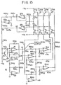
- Fig. 15 shows a sine-wave oscillator which is embodied based on the block configurations of Figs. 1 and 12.
- the signals e1, e3 1 , e3 2 and e3 3 as shown in the vector diagram of Fig. 13 can be obtained.
- the output of an amplifier 10 is connected to the non-inverted and inverted inputs thereof, via resistors R12 2 and R14 1 .
- the non-inverted input of the amplifier 10 is grounded through a resistor R12 3 and through the drain-source path of a depletion type N channel FET 12 1 .
- Connected between the gate and drain of the FET 12 1 is a resistor R12 4 .
- the gate thereof is connected through a resistor R12 9 to a negative power source -V E .
- To the resistor R14 1 a series circuit of capacitors C14, and C14 2 is parallel connected. The junction point of the capacitors C14, and C14 2 is connected through a resistor R14 2 to the inverted input of an amplifier 22.
- the non-inverted input of the amplifier 22 is grounded and the inverted input and output thereof are coupled with each other via a resistor R18 1 .
- the output of the amplifier 22 is coupled with the output of the amplifier 10, via a series circuit of resistors R18 3 and R18 4 .
- the oscillation circuit 16 having such configuration is substantially the same as the oscillation circuit 16 shown in Fig. 2. Difference between these oscillation circuits are merely the difference of the device, i.e. used for the impedance controlled element 12, is a photo-coupler or an FET.
- the junction point of the resistors R18 3 and R18 4 is connected to a non-inverted input of an amplifier 18 20 .
- An output of the amplifier 18 20 is connected through a resistor R18 21 to an inverted input thereof.
- the inverted input of the amplifier 18 20 is grounded via a resistor R18 20 .
- Applied to the non-inverted input of the amplifier 18 20 is a phase-shifted signal e3 whose phase is advanced by 90° from the oscillation output signal e1 which is obtained from the output of the amplifier 10.
- the signal e3 is converted to a signal e3 2 , whose amplitude is same as that of the signal e1, by amplifying A 2 through the amplifier 18 20 .
- the phase of the signal e3 2 is advanced by 90° from that of the signal e1.
- the amplification factor A 2 can be adjusted by the resistor R18 21 .
- the output of the amplifier 10 and the output of the amplifier 18 20 are connected to a non-inverted input of an amplifier 18 10 through a resistor R18 10 and a resistor R18 11 , respectively.
- the non-inverted input of the amplifier 18 10 is grounded via a resistor R18 12 .
- An inverted input of the amplifier 18 10 is connected to an output thereof.
- the composition of the signals e1 and e3 2 is performed at the junction point of the resistors R18 10 and R18 11 .
- the amplitude of the composed signal e1+e3 2 can be adjusted by the resistor R18 12 .
- a signal e3 1 derived from the output of the amplifier 18 10 has the same amplitude as that of the signal e1 and is phase-advanced by 45° from the signal e1.
- the output of the amplifier 10 is connected through a resistor R18 6 to an inverted input of an amplifier 18 00 .
- a resistor R18 7 Connected between the inverted input and output of the amplifier 18 00 is a resistor R18 7 .
- the non-inverted input of the amplifier 18 00 is grounded.
- the output of the amplifier 18 20 and the output of the amplifier 18 00 are coupled with a non-inverted input of an amplifier 18 30 through a resistor R18 30 and a resistor R18 31 , respectively.
- the non-inverted input of the amplifier 18 30 is grounded via a resistor R18 32 .
- An inverted input of the amplifier 18 30 is connected to an output thereof.
- Composition of the signal e3 2 and the signal -e1 is carried out at the junction point of the resistors R18 30 and R18 31 .
- the amplitude of the composed signal e3 2 -e1 can be adjusted by the resistor R18 32 .
- a signal e3 3 derived from the output of the amplifier 18 30 having the same amplitude as that of the signal e1 is phase-advanced by 135° from the signal e1.
- the output of the amplifier 10 is connected through a resistor R18 5 to the base of an NPN transistor 21 11 and the base of a PNP transistor 21 12 .
- the output of the amplifier 18 10 is connected through a resistor R18 13 to the base of an NPN transistor 21 13 and the base of a PNP transistor 21 14 .
- the output of the amplifier 18 20 is connected to the bases of NPN transistor 21 15 and PNP transistor 21 16 , via a resistor R18 23 .
- the output of the amplifier 18 30 is connected to the bases of NPN transistor 21 17 and PNP transistor 21 18 , via a resistor R18 33 .
- the collectors of the transistors 21 11 , 21 13 , 21 15 and 21 17 are connected to a positive power source +V c .
- the collectors of the transistors 21 12 , 21 14 , 21 16 and 21 18 are connected to a negative power source -V E .
- the emitters of the transistors 21 11 , 21 13 , 21 15 and 21 17 are grounded via a parallel circuit of a capacitor C21, and a resistor R21 1 .
- the emitters of the transistors 21 12 , 21 14 , 21 16 and 21 18 are grounded through a parallel circuit of a capacitor C21 2 and a resistor R21 2 .
- the transistors 21 11 to 21 18' capacitors C21, and C21 2 , and resistors R21, and R21 2 constitute the absolute peak value detectors 21 0 to 21 3 . In this configuration the rectifying function between the base-emitter paths of the transistors 21 11 to 21 18 are applied.
- the response speed for an amplitude control of the oscillation output signal e1 is fast. Because, it can be enlarged an amount of charges per unit time, which charges are supplied to the capacitors C21, and C21 2 , by the current-amplification function of the transistors 21 11 to 21 18 . That is, if we consider the emitter output impedances of the transistors 21 11 to 21 18 are Re, the capacitors C21, and C21 2 are charged with time constants C21 1 Re and C21 2 Re, respectively. While, discharge time constants of these CR circuits are C21 1 R21 1 and C21 2 R21 2 .
- the emitter of the transistor 21 11 is connected to a non-inverted input of an amplifier 23 1 .
- An output of the amplifier 23, is connected to an inverted input thereof.
- the emitter of the transistor 21 12 is connected to a non-inverted input of an amplifier 23 2 .
- An output of the amplifier 23 2 is connected to an inverted input thereof.
- the output of the amplifier 23 2 is connected through a resistor R23, to an inverted input of an amplifier 23 3 .
- a non-inverted input of the amplifier 23 3 is grounded.
- An output of the amplifier 23 3 is connected to the inverted input thereof via a resistor R23 2 .
- the outputs of the amplifiers 23 3 and 23, are coupled through a series circuit of resistors R23 3 and R23 4 .
- the junction point of the resistors R23 3 and R23 4 is connected to the gate of an FET 12, through a resistor R12 5 .
- the junction point of the resistors R23 3 and R23 4 provides the control signal e4.
- the amplifiers 23, to 23 3 and the resistors R23, to R23 4 constitute the adder 23.
- the minimum ripple point of the control signal e4 can be obtained by adjusting each of the resistors R18 1 , R18 12 , R18 21 , R18 32 and R23 2 .
- phase-shifting oscillation circuit which includes cascade-connected CR integrators or CR differentiators of 3-stage or more stage, may be applied for the oscillation circuit 16.
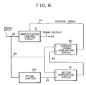
- Fig. 16 shows a basic configuration of an ALC (Automatic Level Control) circuit or a volume expander circuit, which is an application of this invention.
- a phase shifter 140 may be conventional one.
- a phase shift amount of the shifter 140 is selected to 90°.
- a preferable phase shift amount of the shifter 140 is 45°.
- an amplitude control circuit of the invention is suitable for a CR (or LR, LC) type oscillator with an oscillation frequency range below about 1 MHz. Particularly, by using a circuit configuration as shown in Fig. 2, it should be watched that a low-distortion sine-wave generator within extremely low frequency range of about 1 Hz or less can be obtained.
- a circuit configuration (18+20) for controlling the amplitude of oscillator according to the invention can be applicable to an ALC (Automatic Level Control) circuit or AGC (Automatic Gain Control) circuit.
- ALC Automatic Level Control
- AGC Automatic Gain Control
- the vector composition circuit 18 and the control signal generation circuit 20 shown in Fig. 2 or Fig. 15 may directly be applied to an ALC or AGC circuit.
- a configuration corresponding to the amplification control circuit 12 corresponds to an attenuator which is level controlled automatically.
Abstract
Description
- The present invention relates to an amplitude control circuit suitable for stabilizing the oscillation output level of a sine wave oscillator and also suitable for dynamically controlling the signal output level of an automatic level control (ALC) circuit.
- In an amplitude control circuit of oscillators or ALC circuits the level or amplitude change of an output or an input signal must be quickly detected. Namely, a quick response characteristic is required for a control circuit of sine wave oscillators or ALC circuits.
- In order to realize the quick response the time constant of a ripple filter provided in the control signal circuit path has to be as small as possible. However, a small time constant increases ripples of the control signal, resulting in high distortion factor. Accordingly, the quick response and the low distortion factor are contradictory to each other.
- The above contradiction is almost solved by a technical idea disclosed in Japanese Patent Disclosure No. 52-119151. This Disclosure teaches that the quick response can be obtained by the


- The complete ripple-less composition utilized in the above Disclosure requires a precise "f(x)=x 2 " type functional converter circuit. If a precise square conversion is not performed, the control signal involves a little ripple as shown in Fig. 4C, and such ripple worsens the distortion factor. This Disclosure as well as other prior art do not show a specific square conversion circuit having a strict preciseness. Although the amount of ripples in this Disclosure will not be large, nevertheless, a little residual ripple involved therein limits the approach to a low distortion sine wave oscillator.
- In "Toute L'Eiectronique: Nov. 1977, 85-87" a circuit for generating polyphase signals is described. On the other hand, it is not possible to obtain a ripple-free control signal without using a large time constant filter using this known circuit.
- It is accordingly the object of the invention to provide an amplitude control circuit which quickly responds to the amplitude change of an objective signal to be controlled and thus avoiding hunting phenomena, and which is free from residual ripples.
- The above problem is solved by an amplitude control circuit for analog signals comprising:
- amplification control means for amplifying an input signal (ei) with a given gain (eo/ei) controlled by a signal (e4) to provide an output signal (eo);
- signal composer means for phase-shifting said input signal (ei) by a given amount to provide a plurality of polyphase signals each having a given phase difference from said input signal (ei); and
- control signal means for combining said polyphase signals (e31-e3n) to generate the control signal (e4),
- wherein wave forms of said polyphase signals (e3i -e3n) are overlapped with one another so that ripples involved in the envelope of said polyphase signals decrease, and said control signal means includes rectifying means and filter means having defined charge/discharge time constants for further reducing ripple components of said' control signal (e4) which corresponds to the amplitude of said input signal (ei), which is characterized in that one of the defined charge/ discharge time constants of said filter means at the time when the amplitude of said input signal (ei) increases is smaller than the other of said charge/discharge time constants of said filter means at the time when the amplitude of said input signal (ei) decreases.
-
- Fig. 1 is a block diagram showing a basic configuration of sine-wave oscillator which includes an amplitude control circuit according to the invention;
- Fig. 2 is a circuit diagram showing an embodiment of Fig. 1;
- Figs. 3A and 3B are vector diagrams useful explaining a vector-composition by the
vector composition circuit 18 of Fig. 1; - Figs. 4A to 4C show waveforms of sine-waves ±e1a, cosine-waves ±e3a and a control signal e4a indicated in the circuit of Fig. 2;
- Fig. 5 is a graph showing an example of a gate voltage-drain current characteristic of P channel FETs 29 to 34 shown in Fig. 2;
- Fig. 6 is a modification of the
oscillation circuit 16 shown in Fig. 2; - Fig. 7 is a block diagram showing a modification of the square-function composing circuit included in the control
signal generation circuit 20 of Fig. 2; - Fig. 8 is an embodied circuit of the square-
function circuit 72, 76 of Fig. 7; - Figs. 9 to 11 show modifications of the
oscillation circuit 16 of Fig. 2; - Fig. 12 is a block diagram which shows modified configuration of the
vector composition circuit 18 and the controlsignal generation circuit 20 of Fig. 1; - Fig. 13 shows a vector diagram of signals produced in the blocks of Fig. 12;
- Fig. 14 shows a waveform diagram indicating how a control signal e4 is obtained at the condition "n=3" of Fig. 12 configuration;
- Fig. 15 is an embodied circuit of Fig. 12 configuration; and
- Fig. 16 is a block diagram in which the amplitude control circuit of Fig. 1 is applied to an automatic level control circuit.
- Now the preferred embodiments of the invention with be described below. In the description same or like portions are indicated by same or like reference numerals to avoid redundant explanation.
- Fig. 1 shows a basic configuration of sine-wave oscillator which includes an amplitude control circuit according to the invention. An output . signal e1 of an
amplifier circuit 10 is input to anamplification control circuit 12. The signal e1 is positively (or negatively) fed back to a first input of theamplifier 10 through thecontrol circuit 12. Also the signal e1 is negatively (or positively) fed back to a second input of theamplifier 10 via an oscillationfrequency setting circuit 14. Thecircuit components conventional oscillation circuit 16. Suppose that the signals supplied to the first and second input of theamplifier 10 are, e.g., positive and negative feedback signals, respectively. In this case, theoscillation circuit 16 forms Sulzer type (Bridged T type) oscillator. On the contrary signals supplied to the first and second inputs are negative and positive feedback signals, theoscillation circuit 16 forms Wienbridge type oscillator. - The signal e1 is supplied to a first input of a
vector composition circuit 18. A second input of thecomposition circuit 18 is supplied with a phase-shifted signal e2 which is derived from thesetting circuit 14. When Sulzer type or Wien- bridge type is applied to thesetting circuit 14, a phase-shift amount about 45° of the signal e2 as against the signal e1 can be obtained. The signals e1 and e2 are converted into a signal e3 whose phase is shifted by 90° from the signal e1, by means of thecomposition circuit 18. For example, when the signal e1 is a sine-wave, the signal e3 is a cosine-wave. Also the signal e1 is supplied to a first input of a controlsignal generation circuit 20. A second input of thegeneration circuit 20 is supplied with the signal e3. - The control
signal generation circuit 20 synthesizes a control signal e4 which includes a DC component proportional to the sum of squared signals e1 and e3. That is, the DC component of the signal e4 can be explained by a function with parameter of e12+e32. Suppose that the signals e1 and e3 are defined as below:


generation circuit 20. Clearly anticipated from the equation (3), the signal e4 is independent of the angular frequency ω of the oscillation output signal e1. The signal e4 only contains information proportional to the square of amplitude E of the signal e1. By the signal e4 the transfer function of thecontrol circuit 12 is controlled. - Fig. 2 is a detail circuit diagram of the basic configuration shown in Fig. 1. The inventor believes that this circuit configuration is a best mode at the time the application is filed.
- An output of an
amplifier 10 is connnected via a resistor R122 to a non-inverted input of theamplifier 10. The non-inverted input is grounded through a resistance R12, of an impedance controlledelement 121. For theelement 12, a photo-coupler combining LED and CdS cell is preferably applied. Theelement 12, and the resistor R122 form theamplification control circuit 12. An inverted input of theamplifier 10 is connected to the output thereof, through a resistor R141. A series circuit of capacitors C14, and C142 is parallel connected to the resistor R141. The connection point of capacitors C14, and C142 is connected via a resistor R142 to an inverted input of anamplifier 22. The resistors R141, R142 and the capacitors C141, C142 form the oscillationfrequency setting circuit 14 of Bridged Ttype. Theamplifier 10, impedance controlledelement 121, resistors R122, R141, R142 and capacitors C14,, C142 constitute theoscillation circuit 16. - The inverted input of the
amplifier 22 is connected to an output thereof via a resistor R181. A non-inverted input of theamplifier 22 is grounded through a resistor R182. The resistor R182 is provided for an off-set balancing. The output of theamplifier 22 is connected to the output of theamplifier 10 through a series circuit of resistors R183 and R184. Theamplifier 22 and the resistors R18, to R184 form thevector composition circuit 18. The inverted input of theamplifier 22 is in the state of "imaginary ground". That is, the junction point of the resistors R142 and R181 is equivalently grounded. At the connection point of the capacitor C14, and C142 in the oscillationfrequency setting circuit 14, the phase-shifted signal e2 appears. The phase-shifted signal e2 is a sine-wave voltage signal having a phase difference φ from the sine-wave oscillation output signal e1 of theoscillation circuit 16. The signal e2 is converted to a current signal i2 corresponding to e2/R142 and input to thevector composition circuit 18. The current signal i2 is converted into a phase-shifted signal e2a by theamplifier 22. The phase-shifted signal e2a is antiphased from the signal e2. The amplitude of the signal e2a can be varied by the resistor R181. The phase-shifted signal e2a and the oscillation output signal e1 are added by an adder circuit being formed of the resistors R183 and R184. By this addition a phase-shifted signal e3 whose phase is differenced by 90° from the signal e1, is obtained. - Reference should be made to Fig. 3A. This figure illustrates how the composition of the phase-shifted signal e3 is performed in the
vector composition circuit 18. Now we suppose that the phase-shifted signal e2 is phase-delayed by φ from the oscillation output signal e1. To invert the phase of the signal e2 and amplify its amplitude by Ai, the phase-shifted signal e2a is obtained. By vector-summing the signal e2a and the signal e1 a phase-shifted signal e3 is composed. The phase difference between the signal e1 and the signal e3 can be set at 90° by adjusting the amplitude rate Ai. Namely, thevector composition circuit 18 composes a cosine-wave signal from a sine-wave signal. A 90° phase-shifted signal Aze3 whose amplitude is equal to the oscillation output signal e1, is obtained from amplifying the signal e3 by A2. - Reference should return to Fig. 2, in which the output of the
amplifier 10 is connected to an inverted input of anamplifier 24, through a series circuit of resistors R201 and R202. The inverted input of theamplifier 24 is coupled with its output via a resistor R203. A non-inverted input of theamplifier 24 is grounded by way of a resistor R204 for off-set balancing. The junction point of the resistors R183 and R184 is connected to an inverted input of anamplifier 26, through a series circuit of resistors R205 and R206. The inverted input of theamplifier 26 is coupled with its output via a resistor R207. A non-inverted input of theamplifier 26 is grounded by way of a resistor R208. - In the circuit configuration above-mentioned, suppose that R20z=R203 and R206=R207. In this case, when a signal appeared at the junction point of the resistors R20, and R202 is deemed as e1a, a signal appeared at the output of the
amplifier 24 is -e1a. Similarly, a signal at the junction point of the resistors R205 and R206 as e3a, a signal at the output of theamplifier 26 as -e3a. The signal e1a a is in-phase with the oscillation output signal e1 and the signal e3a is in-phase with the phase-shifted signal e3. Accordingly a phase difference of 90° is presented between the signals e1a and e3a. Amplitudes of the signals e1a a and e3a can be adjusted by the resistors R20, and R205, respectively. The amplitudes of signals e1a and e3a can therefore be set to equal each other. The phase relations of the signals e1a, -e1a and the signals e3a, -e3a are respectively shown in Figs. 4A and 4B. - Reference should be made to Fig. 2, again. The junction point of the resistors R201 and R202 is connected to the gate of a P
channel MOS FET 28. The output of theamplifier 24 is connected to the gate of a Pchannel MOS FET 30. Similarly, the junction point of R205 and R206 and the output of theamplifier 26 are connected to the gates of Pchannel MOS FETs FETs 28 to 34. However, any type of device may be used whose characteristic of drain current ID can substantially be represented by a square-function of its gate-source voltage VGS. For example, a depletion type may be applied toFETs 28 to 34. The chief reason for applying an enhancement type FETs in Fig. 2 is that the circuit configuration can easily be simplified. Fig. 5 shows a typical ID-VGS characteristic of P channel FET. In this figure, a curve "A" indicates an enhancement type and -VTH designates its threshold voltage. A curve "B" indicates a depletion type and +Vp designates its pinch-off voltage. Generally the curves "A", "B" can be represented by a square-function with good accuracy. - In Fig. 2, the drains of
FETs FETs FETs NPN transistor 36. Also, each substrate and source ofFETs NPN transistor 38. The bases of thetransistors NPN transistor 40. The emitter of thetransistor 40 is grounded through a resistor R2011. The collector of thetransistor 40 is connected to a positive power source +Vc via a resistor R2012. The diode-connectedtransistor 40 is provided for temperature-compensation of the base-emitter threshold voltages VBE of thetransistors FETs 28 to 34 can be adjusted by the resistor R2012. In this circuit, "dual" type, in which electrical characteristics of packed pellets are matched, are suitable for theFETs FETs - The collectors of the
transistors element 121. The anode of the LED is connected to the positive power source +Vc. The collectors of thetransistors amplification control circuit 12. If the ID-VGS characteristics of theFETs 28 to 34 may completely be regarded as a square function, the control current I4 does not involve the ripples. However, where the ID-VGS characteristics do not meet at the square function the current I4 includes some ripples. Frequency components of the ripple are higher harmonics over second order of the oscillation output signal e1's frequency. Moreover the amplitude of the ripple component is extremely small as compared with the DC level of the control current I4. The time constant may therefore be small, which is formed of the capacitor C201 and the corrector circuit impedance of thetransistors - The
amplifiers FETs 28 to 34,transistors 36 to 40, resistors R201 to R2013 and the capacitor C20, are constituting the controlsignal generation circuit 20. - The composing operation of the control current 14, i.e. the control signal e4 as set forth in equation (3), can be explained as described below. This explanation will be made by referring Figs. 4 and 5. Suppose that, in Fig. 2, the source-potentials of
FETs 28 to 34 are adjusted at the threshold voltage +VTH. This means that the gate voltage -VGS to the sources ofFETs FETs FET 28 is cut-off during the positive half period of the signal e1a. while the negative half period of the signal e1a, a current i28 proportional to e1a2 is flowing into the source-drain path ofFET 28. Similarly, only the negative half period of the signal -e1a or the positive half period of the signal e1a, a current i30 proportional to (-e1 a)2 is flowing into theFET 30. Then a current i28+i30 proportional to e1a2 flows in the collector circuit of thetransistor 36 along the whole phase. - In the same way, a current i32 proportional to e3az and a current i34 to (-e3a)2 are flowing into the
FETs transistor 38 along the whole phase. The sum of the currents iz8, i30, i32 and i34 provides the control current I4. A collector voltage e4a of thetransistors - By applying the amplitude control circuit of this invention, a stable oscillation output signal can be obtained irrespective of its oscillation frequency. Accordingly, an extreme low frequency sine-wave signal, which has only been put to practical use by a function generator, can be obtained by a conventional Sulzer type or Wien-bridge type oscillator circuit with this invention.
- Hitherto a function generator is widely used for an extremely low frequency band sine-wave oscillator. In the function generator a sine-wave is composed from a triangle-wave by functional conversion of f(x)=sin x/x. Accurate conversion of this function is difficult, technically. It is therefore hard to obtain a low distortion sine-wave from a triangle-wave. Further, a sine-wave obtained from this functional conversion is attended with a large distortion including much higher harmonics of odd number order. On the contrary, by the configuration of Fig. 2, an extremely low frequency sine-wave signal e1 with low distortion factor can be obtained.
- Fig. 6 shows a modification of
oscillation circuit 16 applicable to this invention. In this circuit a bootstrap type positive feedback circuit is applied to the oscillationfrequency setting circuit 14. This positive feedback circuit is one modification of another Japanese Patent Application "Band Rejection Circuit" which is made by the same inventor. This application is Japanese Patent Application No. 145981/76 filed on December 4, 1976 and is amended on August 23, 1977. - A positive feedback circuit of the
amplifier 10 or theamplification control circuit 12 has the same configuration of Fig. 2. On the other hand the negative feedback circuit is constructed as below. The output of theamplifier 10 is connected to a non-inverted input of anamplifier 141, via a series circuit of resistors R14, and R142. The junction point of the resistors R14, and R142 is connected through a capacitor C14, to an output of theamplifier 141. The output of theamplifier 14, is connected through a resistor R144 to an inverted input thereof. The inverted input of theamplifier 14, is grounded via a resistor R145. The non-inverted input of theamplifier 14, is connected through a capacitor C142 to the non-inverted input of theamplifier 10. The non-inverted input of theamplifier 10 is grounded via a resistor R143. - In this circuit, when an amplitude A14 of the
amplifier 14, is "1", or R144/R145=0, the oscillation frequency can be varied by the capacitors C14, and/or C142. It is undesirable to use the resistors R141 and/or R142 for varying the oscillation frequency, when A14=1. If the resistor R141 or R142 is varied, the negative feedback amount of theamplifier 10 at the oscillation frequency is also varied in accordance with the variance of the resistor. This makes the amplitude of the oscillation output signal e1 changed. In the extreme case, the output signal e1 may be clipped or the oscillation be stopped. However, when the resistors R141, R142 and R143 is so varied as to hold the relation
- Suppose that the following relation is held.


- When the relation (4) or (5) is held, if the oscillation frequency is varied by R141, no amplitude variation is occurred in the oscillation output signal e1. In the case where A14=2 and C141=C142, for example, the relation (4) or (5) is satisfied. In this case, the transfer function at the oscillation frequency from the output of the
amplifier 10 to the non-inverted input thereof, is independent of the resistor R141. Thus, the oscillation frequency may be varied by changing the resistor R141. Detail description relating to the theoretical analysis of the relations mentioned above is set forth on the amended specification of said Japanese Patent Application No. 145981/76. - In the
oscillation circuit 16 of Fig. 6, there is an advantage that a device (resistor or capacitor) for varying the oscillation frequency may be single. This means that such a circuit is particularly suitable to constitute a voltage controlled oscillator (VCO). On the other hand, in an oscillation circuit of Sulzer or Wien-bridge type, at least a two-ganged or more ganged type variable resistor or variable capacitor (variable condenser) is required for varying the oscillation frequency, and when such a ganged device includes a gang-error the amplitude of the oscillation output e1 is liable to vary with varying the oscillation frequency. - Fig. 7 shows a modification of the square function composition circuit in the control
signal generation circuit 20. In the case of Fig. 2 a square function characteristic between the gate-source voltage VGS and the drain current ID of FETs 28-34 is applied. Further, a full-wave rectification for the signals e1 and e2 is realized by theFETs 28 to 34 such that these FETs are cut-off during the positive half period of ±e1 and ±e3. Such a full-wave rectification and square function composition of theFETs 28 to 34 may be realized by a general configuration as shown in Fig. 7. In this configuration the signal e1 is converted to, for example, a pulsation signal e1a of positive period of sine-wave by a full-wave rectifier 70. The signal e1a is converted to a squared signal e1a2 by asquare function circuit 72. Similarly the signal e3 is converted to a squared signal e3az through a full-wave rectifier 74 and a square function circuit 76. The squared signals e1a2 and e3a2 is added by anadder 78. Then theadder 78 provides the squared signal
- The full-
wave rectifiers square function circuit 72, 76 and theadder 78 may be conventional ones. For therectifier 70 or 74 a linear rectifier circuit, which comprises an operational amplifier whose negative feedback loop includes a rectifying diode or a rectifying transistor, is suitable. For thesquare function circuit 72 or 76, following circuit means is suitable. - (a) By means of a tangential approximation using diodes.
- (b) By means of a combination of log-compressor, doubler amplifier and exponential function circuit. For example, an input signal e1 is converted through the log-compressor to log e1. This log e1 is doubled by the doubler amplifier and is converted to 2 log e1=log e12. This log e12 is converted to exp (log e12)=e12, via the exponential function circuit.
- (c) By means of an application of √type (root or radical type) voltage-current characteristic which appears in a low voltage range of a drain current and drain-source voltage property of an FET. A circuit example of such means is shown in Fig. 8.
- An output of an
amplifier 72, is connected to the drain of an N channeldepletion type FET 722. The source of theFET 722 is connected to an inverted input of theamplifier 721. The inverted input is grounded via a resistor R721. Connected between the source and gate of the FET is a gate-bias voltage source 723. The curve of the drain current and source-drain voltage of theFET 722 can be varied by changing the voltage of thesource 723. When a positive potential signal e1a with a given amplitude is input to a non-inverted input of theamplifier 721, a signal nearly proportional to e1a2 is obtained from the output of theamplifier 721. - Figs. 9 through 12 show modifications of the
oscillation circuit 16 shown in Fig. 2. In Fig. 9 a resistor R122 within an impedance controlledelement 12, included in theamplification control circuit 12 is connected between the non-inverted input and output of anamplifier 10. When the amplitude of the oscillation output signal e1 is increased, a current l4 supplied to a lamp included in theelement 12, is decreased. In this figure the decrease of the current 14 is indicated by-l4 which marked with a negative sign. With decrease of the current 14, the resistance value of the resistor R122 is increased, then the amplitude of the signal e1 is decreased. Further, for the oscillationfrequency setting circuit 14, a capacitor C14, is used as a bridging element, and the supplement of said oscillation circuit current i2 is carried out through a capacitor C142. - In Fig. 10, a Wien-bridge type oscillation circuit is employed for the
oscillation circuit 16. The output of anamplifier 10 is connected through a resistor R122 to the inverted input thereof. The inverted input of theamplifier 10 is grounded, via a resistor R123 and the drain-source path of anN channel FET 121. For thisFET 12, a depletion type is considered. When an enhancement type or P channel type FET is used for theFET 121, a biasing method or a polarity of the control signal e4a should be changed. Connected between the drain gate path of theFET 12, is a resistor R124. The resistor R124 is employed in a negative feedback to compensate the non-linearity of the inner resistance (R-121) of theFET 12,. By the negative feedback operation, drain voltage-drain current characteristic of theFET 12, displays a non- saturation curve which is so-called "triode characteristic". When such a negative feedback is used, substituting a bipolar transistor for theFET 12, may be done. Even though by employing abipolar transistor 121, said triode characteristic can apparently be obtained. To the gate of theFET 12, a control signal e4a is applied through a resistor R125. In Fig. 10 the control signal e4a is marked with negative sign. This negative sign denotes that the amplitude increment of the oscillation output signal e1 makes the potential of the control signal e4a lowered. That is, the negative control signal -e4a is proportional to the amplitude of the oscillation output signal e1. - The output of the
amplifier 10 is connected to the non-inverted input thereof, via a series circuit of a capacitor C14, and a resistor R141. The non-inverted input of theamplifier 10 is grounded through a parallel circuit of a resistor R142 and a capacitor C142. The junction point of the resistor R14, and the capacitor C14, is connected to a non-inverted input of anamplifier 142. An inverted input of theamplifier 142 is connected to an output thereof. The phase-shifted signal e2 is derived from the output of theamplifier 142. Theamplifier 142 is merely provided for an impedance converter. In theoscillation circuit 16 of Fig. 10, the phase-shifted direction of the signal e2 is opposite to that of Fig. 2. In this case the composition of a 90° phase-shifted signal e3 is performed as shown in Fig. 3B. - Fig. 11 shows a modification of the
oscillation circuit 16 shown in Fig. 10. The output of theamplifier 10 is connected to the non-inverted input thereof, through a series circuit of a resistor R14, and a capacitor C141. The non-inverted input of theamplifier 10 is grounded, via a parallel circuit of a resistor R142 and a capacitor C142. The output of theamplifier 10 is connected through a resistor R122 to the inverted input thereof. The inverted input of theamplifier 10 is grounded via a resistor R123. The output of theamplifier 10 is connected through a resistor R126 to an inverted input of anamplifier 143. The inverted input of theamplifier 143 is connected to an output thereof via a resistor R127. A non-inverted input of theamplifier 143 is grounded. - Connected between the inverted input of
amplifier 10 and the output ofamplifier 143 is the drain-source path of an enhancement type Pchannel MOS.FET 121. The substrate of theFET 121 is grounded. The gate of theFET 12, is connected through a resistor R124 to the drain (or source) thereof. The gate is also connected to the source (or drain) via a resistor R128. To the gate of theFET 12, the control signal e4a is supplied through a resistor R125. The gate is connected through a resistor R129 to a negative power source -VE for biasing theFET 121. The phase-shifted signal e2 is derived from the junction point of the resistor R14, and the capacitor C141. - In the
oscillation circuit 16 of Fig. 11, suppose that the drain-source structure of theFET 12, is symmetrical with respect to the gate and R124=R128, and that the amplitude of a signal e10 at the inverted input of theamplifier 10 is same as that of a signal e14 at the output of theamplifier 143 by adjusting the value of a resistance ratio R127/R126. Then, the drain and source of theFET 12, are applied with the signals e10 and e14 which have the same amplitude and antiphase relation with each other with respect to the substrate potential. Thus, theFET 12, is driven in a condition of "Push-Pull". Such configuration is well fitted for amplitude-controlling of a large amplitude signal. The resistors R124 and R128 is used for compensating the non-linearity of inner resistance of theFET 121. However, an oscillation output signal e1 with relatively low distortion can be obtained without using the resistors R124 and R128 when the amplitude of a signal applied to theFET 12, is small. By fine-adjusting the amount of a resistance ratio R127/R126, a minimum point of distortion of the oscillation output signal e1 can be attained. - Fig. 12 shows a modification of the basic configuration of Fig. 1. In Fig. 1, a signal e2=sin (ωt-φ) is converted to e3=cos wt by the
vector composition circuit 18, and a control signal e4=e12+e32, which does substantially not include ripples, is obtained from the controlsignal generation circuit 20. On the contrary, in Fig. 12, "n" kinds of phase-shifted signals e3n are composed by "n" blocks ofvector composition circuits 18n. The control signal e4 is obtained from summing the absolute peak values of these signals e3n. Thus, Fig. 12 shows a configuration embodying the following equation:
- The oscillation output signal e1 is applied to an absolute peak value detector 210 and the first input of
vector composition circuits 181 to 18n. Thecircuits 181 to 18n compose phase-shifted signals e31 to e3n based on the signals e1 and e2. Each of thecomposition circuits 181 to 18n may have the same configuration as that of thecomposition circuit 18 shown in Fig. 2. Signals e31 to e3n composed by thecircuits 181 to 18n, respectively, are input to absolute peak value detectors 211 to 21 n. The signals e31 to e3n are converted to absolute peak value signals
adder 23. - Fig. 13 shows an example of vector diagram wherein "n=3" is applied to the equation (6). In this example, phase differences of the signals e1, e31, e32 and e33 are 45°. If the phase-shift amount of the phase-shifted signal e2 is originally 45°, the vector composition at the time of n=3 can easily be accomplished.
- Fig. 14 shows an envelope of the control signal e4 which is composed in the case of n=3. Ripples of the peak of the signals e1, e31, e32 and e33 applied to the
adder 23 are small. The time constants of charge-discharge circuits of the detectors 210 to 213 may therefore be relatively small. - Fig. 15 shows a sine-wave oscillator which is embodied based on the block configurations of Figs. 1 and 12. By the circuit configuration of Fig. 15, the signals e1, e31, e32 and e33 as shown in the vector diagram of Fig. 13 can be obtained.
- The output of an
amplifier 10 is connected to the non-inverted and inverted inputs thereof, via resistors R122 and R141. The non-inverted input of theamplifier 10 is grounded through a resistor R123 and through the drain-source path of a depletion typeN channel FET 121. Connected between the gate and drain of theFET 121 is a resistor R124. For biasing theFET 12, the gate thereof is connected through a resistor R129 to a negative power source -VE. To the resistor R141 a series circuit of capacitors C14, and C142 is parallel connected. The junction point of the capacitors C14, and C142 is connected through a resistor R142 to the inverted input of anamplifier 22. The non-inverted input of theamplifier 22 is grounded and the inverted input and output thereof are coupled with each other via a resistor R181. The output of theamplifier 22 is coupled with the output of theamplifier 10, via a series circuit of resistors R183 and R184. Theoscillation circuit 16 having such configuration is substantially the same as theoscillation circuit 16 shown in Fig. 2. Difference between these oscillation circuits are merely the difference of the device, i.e. used for the impedance controlledelement 12, is a photo-coupler or an FET. - The junction point of the resistors R183 and R184 is connected to a non-inverted input of an
amplifier 1820. An output of theamplifier 1820 is connected through a resistor R1821 to an inverted input thereof. The inverted input of theamplifier 1820 is grounded via a resistor R1820. Applied to the non-inverted input of theamplifier 1820 is a phase-shifted signal e3 whose phase is advanced by 90° from the oscillation output signal e1 which is obtained from the output of theamplifier 10. The signal e3 is converted to a signal e32, whose amplitude is same as that of the signal e1, by amplifying A2 through theamplifier 1820. The phase of the signal e32 is advanced by 90° from that of the signal e1. The amplification factor A2 can be adjusted by the resistor R1821. - The output of the
amplifier 10 and the output of theamplifier 1820 are connected to a non-inverted input of anamplifier 1810 through a resistor R1810 and a resistor R1811, respectively. The non-inverted input of theamplifier 1810 is grounded via a resistor R1812. An inverted input of theamplifier 1810 is connected to an output thereof. The composition of the signals e1 and e32 is performed at the junction point of the resistors R1810 and R1811. The amplitude of the composed signal e1+e32 can be adjusted by the resistor R1812. Suppose that the voltage dividing ratio of the resistors R1810, R1811 and R1812 is 1/√2 and R181O=R1811. In this situation a signal e31 derived from the output of theamplifier 1810 has the same amplitude as that of the signal e1 and is phase-advanced by 45° from the signal e1. - The output of the
amplifier 10 is connected through a resistor R186 to an inverted input of anamplifier 1800. Connected between the inverted input and output of theamplifier 1800 is a resistor R187. The non-inverted input of theamplifier 1800 is grounded. In the case where R186=R187, obtained from the output of theamplifier 1800 is a signal -e1 which has the same amplitude as that of the signal e1 and has an anti-phase relation with the signal e1. The output of theamplifier 1820 and the output of theamplifier 1800 are coupled with a non-inverted input of anamplifier 1830 through a resistor R1830 and a resistor R1831, respectively. The non-inverted input of theamplifier 1830 is grounded via a resistor R1832. An inverted input of theamplifier 1830 is connected to an output thereof. Composition of the signal e32 and the signal -e1 is carried out at the junction point of the resistors R1830 and R1831. The amplitude of the composed signal e32-e1 can be adjusted by the resistor R1832. A signal e33 derived from the output of theamplifier 1830 having the same amplitude as that of the signal e1 is phase-advanced by 135° from the signal e1. - The output of the
amplifier 10 is connected through a resistor R185 to the base of an NPN transistor 2111 and the base of a PNP transistor 2112. The output of theamplifier 1810 is connected through a resistor R1813 to the base of an NPN transistor 2113 and the base of a PNP transistor 2114. The output of theamplifier 1820 is connected to the bases of NPN transistor 2115 and PNP transistor 2116, via a resistor R1823. The output of theamplifier 1830 is connected to the bases of NPN transistor 2117 and PNP transistor 2118, via a resistor R1833. The collectors of the transistors 2111, 2113, 2115 and 2117 are connected to a positive power source +Vc. The collectors of the transistors 2112, 2114, 2116 and 2118 are connected to a negative power source -VE. The emitters of the transistors 2111, 2113, 2115 and 2117 are grounded via a parallel circuit of a capacitor C21, and a resistor R211. The emitters of the transistors 2112, 2114, 2116 and 2118 are grounded through a parallel circuit of a capacitor C212 and a resistor R212. The transistors 2111 to 2118' capacitors C21, and C212, and resistors R21, and R212 constitute the absolute peak value detectors 210 to 213. In this configuration the rectifying function between the base-emitter paths of the transistors 2111 to 2118 are applied. - In the case where the base-emitter path of bipolar transistor is applied for a signal rectification as mentioned above, the response speed for an amplitude control of the oscillation output signal e1 is fast. Because, it can be enlarged an amount of charges per unit time, which charges are supplied to the capacitors C21, and C212, by the current-amplification function of the transistors 2111 to 2118. That is, if we consider the emitter output impedances of the transistors 2111 to 2118 are Re, the capacitors C21, and C212 are charged with time constants C211Re and C212Re, respectively. While, discharge time constants of these CR circuits are C211R211 and C212R212. By such circuit configuration of these CR charge/discharge circuits, a fast response speed and a large discharge time constant can be realized, simultaneously. Derived from the outputs of these CR charge/discharge circuits, or the emitters of the transistors 2111 and 2112' are peak potential +E and -E of the signals e1, e31, e32 and e33.
- The emitter of the transistor 2111 is connected to a non-inverted input of an
amplifier 231. An output of theamplifier 23, is connected to an inverted input thereof. The emitter of the transistor 2112 is connected to a non-inverted input of anamplifier 232. An output of theamplifier 232 is connected to an inverted input thereof. The output of theamplifier 232 is connected through a resistor R23, to an inverted input of anamplifier 233. A non-inverted input of theamplifier 233 is grounded. An output of theamplifier 233 is connected to the inverted input thereof via a resistor R232. When R23↑=R232, theamplifier 233 constitutes an inverter with a transfer function of "-1". The outputs of theamplifiers FET 12, through a resistor R125. The junction point of the resistors R233 and R234 provides the control signal e4. Theamplifiers 23, to 233 and the resistors R23, to R234 constitute theadder 23. - The minimum ripple point of the control signal e4 can be obtained by adjusting each of the resistors R181, R1812, R1821, R1832 and R232.
- Although, a phase-shifting oscillation circuit, which includes cascade-connected CR integrators or CR differentiators of 3-stage or more stage, may be applied for the
oscillation circuit 16. - Fig. 16 shows a basic configuration of an ALC (Automatic Level Control) circuit or a volume expander circuit, which is an application of this invention. A
phase shifter 140 may be conventional one. In the case where the Fig. 16 configuration is embodied the same configuration as the circuit of Fig. 2, a phase shift amount of theshifter 140 is selected to 90°. When the circuit configuration of Fig. 15 is applied, a preferable phase shift amount of theshifter 140 is 45°. When the Fig. 16 configuration is applied for an ALC circuit, a transfer function G=e0/ei of the amplitude controlled circuit is small as the amplitude of the input signal e, is large. On the other hand, this configuration is applied for a volume expander circuit, the transfer function G is large as the amplitude of the signal e, is large. In the amplitude controlled circuit of Fig. 16, the control signal e4 does almost not include ripples even though the operation speed of the control is set to fast. From this, the transfer function G is almost not modulated by the ripple component of the control signal e4. - Application of an amplitude control circuit of the invention is suitable for a CR (or LR, LC) type oscillator with an oscillation frequency range below about 1 MHz. Particularly, by using a circuit configuration as shown in Fig. 2, it should be watched that a low-distortion sine-wave generator within extremely low frequency range of about 1 Hz or less can be obtained.
- Further, a circuit configuration (18+20) for controlling the amplitude of oscillator according to the invention can be applicable to an ALC (Automatic Level Control) circuit or AGC (Automatic Gain Control) circuit. Thus, to compose a signal whose phase is shifted from the input signal by a conventional phase shifter, the
vector composition circuit 18 and the controlsignal generation circuit 20 shown in Fig. 2 or Fig. 15 may directly be applied to an ALC or AGC circuit. In this case a configuration corresponding to theamplification control circuit 12 corresponds to an attenuator which is level controlled automatically.
Claims (11)
characterized in that

Applications Claiming Priority (1)
| Application Number | Priority Date | Filing Date | Title |
|---|---|---|---|
| PCT/JP1978/000040 WO1980001224A1 (en) | 1978-12-05 | 1978-12-05 | Amplitude control circuits |
Publications (3)
| Publication Number | Publication Date |
|---|---|
| EP0022866A1 EP0022866A1 (en) | 1981-01-28 |
| EP0022866A4 EP0022866A4 (en) | 1981-03-27 |
| EP0022866B1 true EP0022866B1 (en) | 1985-06-05 |
Family
ID=13649520
Family Applications (1)
| Application Number | Title | Priority Date | Filing Date |
|---|---|---|---|
| EP79900105A Expired EP0022866B1 (en) | 1978-12-05 | 1980-06-17 | Amplitude control circuits |
Country Status (5)
| Country | Link |
|---|---|
| US (1) | US4430627A (en) |
| EP (1) | EP0022866B1 (en) |
| JP (1) | JPS6317242B1 (en) |
| DE (1) | DE2862467D1 (en) |
| WO (1) | WO1980001224A1 (en) |
Families Citing this family (23)
| Publication number | Priority date | Publication date | Assignee | Title |
|---|---|---|---|---|
| US6278338B1 (en) * | 2000-05-01 | 2001-08-21 | Silicon Wave Inc. | Crystal oscillator with peak detector amplitude control |
| US6795843B1 (en) * | 2000-11-08 | 2004-09-21 | Sequoia Communications | Low-distortion differential circuit |
| US7171170B2 (en) | 2001-07-23 | 2007-01-30 | Sequoia Communications | Envelope limiting for polar modulators |
| US6985703B2 (en) | 2001-10-04 | 2006-01-10 | Sequoia Corporation | Direct synthesis transmitter |
| WO2003077046A1 (en) * | 2002-03-13 | 2003-09-18 | Toshiji Kato | Digital control device and program |
| US7489916B1 (en) | 2002-06-04 | 2009-02-10 | Sequoia Communications | Direct down-conversion mixer architecture |
| US6825736B1 (en) * | 2003-05-30 | 2004-11-30 | Freescale Semiconductor, Inc. | Method and apparatus for controlling a voltage controlled oscillator |
| US7609118B1 (en) | 2003-12-29 | 2009-10-27 | Sequoia Communications | Phase-locked loop calibration system |
| US7496338B1 (en) | 2003-12-29 | 2009-02-24 | Sequoia Communications | Multi-segment gain control system |
| US7522017B1 (en) | 2004-04-21 | 2009-04-21 | Sequoia Communications | High-Q integrated RF filters |
| US7672648B1 (en) | 2004-06-26 | 2010-03-02 | Quintics Holdings | System for linear amplitude modulation |
| US7548122B1 (en) | 2005-03-01 | 2009-06-16 | Sequoia Communications | PLL with switched parameters |
| US7479815B1 (en) | 2005-03-01 | 2009-01-20 | Sequoia Communications | PLL with dual edge sensitivity |
| US7675379B1 (en) | 2005-03-05 | 2010-03-09 | Quintics Holdings | Linear wideband phase modulation system |
| US7595626B1 (en) | 2005-05-05 | 2009-09-29 | Sequoia Communications | System for matched and isolated references |
| US20070205200A1 (en) * | 2006-03-02 | 2007-09-06 | Brain Box Concepts | Soap bar holder and method of supporting a soap bar |
| WO2007137094A2 (en) | 2006-05-16 | 2007-11-29 | Sequoia Communications | A multi-mode vco for direct fm systems |
| US7679468B1 (en) | 2006-07-28 | 2010-03-16 | Quintic Holdings | KFM frequency tracking system using a digital correlator |
| US7522005B1 (en) | 2006-07-28 | 2009-04-21 | Sequoia Communications | KFM frequency tracking system using an analog correlator |
| US7894545B1 (en) | 2006-08-14 | 2011-02-22 | Quintic Holdings | Time alignment of polar transmitter |
| US7920033B1 (en) | 2006-09-28 | 2011-04-05 | Groe John B | Systems and methods for frequency modulation adjustment |
| US9099956B2 (en) | 2011-04-26 | 2015-08-04 | King Abdulaziz City For Science And Technology | Injection locking based power amplifier |
| ITVI20120280A1 (en) * | 2012-10-22 | 2014-04-23 | Cartigliano Off Spa | GENERATOR DEVICE FOR AN ALTERNATED ELECTROMAGNETIC FIELD IN RADIO FREQUENCY, METHOD OF CONTROL AND USING SYSTEM OF THIS DEVICE |
Family Cites Families (2)
| Publication number | Priority date | Publication date | Assignee | Title |
|---|---|---|---|---|
| JPS52119151A (en) * | 1976-03-31 | 1977-10-06 | Enuefu Kairo Setsukei Burotsuk | Oscillator |
| DE2714673A1 (en) * | 1976-04-06 | 1977-10-20 | Chauvin Arnoux Sa | Self excited reference or calibration oscillator - has two phase shifting stages whose gains are constant and independent of oscillator frequency |
-
1978
- 1978-12-05 DE DE7979900105T patent/DE2862467D1/en not_active Expired
- 1978-12-05 US US06/212,086 patent/US4430627A/en not_active Expired - Lifetime
- 1978-12-05 WO PCT/JP1978/000040 patent/WO1980001224A1/en unknown
- 1978-12-05 JP JP79500285A patent/JPS6317242B1/ja active Pending
-
1980
- 1980-06-17 EP EP79900105A patent/EP0022866B1/en not_active Expired
Also Published As
| Publication number | Publication date |
|---|---|
| JPS6317242B1 (en) | 1988-04-13 |
| WO1980001224A1 (en) | 1980-06-12 |
| EP0022866A4 (en) | 1981-03-27 |
| DE2862467D1 (en) | 1985-07-11 |
| US4430627A (en) | 1984-02-07 |
| EP0022866A1 (en) | 1981-01-28 |
Similar Documents
| Publication | Publication Date | Title |
|---|---|---|
| EP0022866B1 (en) | Amplitude control circuits | |
| US4514702A (en) | Logarithmic electronic gain control circuit | |
| US4857861A (en) | Amplifier arrangement with improved quiescent current control | |
| US5319303A (en) | Current source circuit | |
| US4220875A (en) | Electronic circuit having its impedance controlled by an external signal | |
| US4462004A (en) | Dynamic class-4 FET amplifier | |
| US5136257A (en) | RF amplifier bias circuit | |
| US4528516A (en) | Differential amplifier with dynamic thermal balancing | |
| EP0025977B1 (en) | Gain controlled amplifier | |
| EP0067163B1 (en) | Linear full wave rectifier circuit | |
| US4342006A (en) | Amplifier circuit for supplying load with output signal current proportional to input signal voltage | |
| US4654607A (en) | Modulation control circuit for an amplitude modulator | |
| US4514701A (en) | Automatic level control circuit | |
| US4625131A (en) | Attenuator circuit | |
| US4490685A (en) | Differential amplifier | |
| US4791385A (en) | Voltage controlled amplifier for symmetrical electrical signals | |
| US4439696A (en) | Dividing circuit | |
| US4360866A (en) | Linear full wave rectifier and method for providing full wave rectified signals | |
| US4567441A (en) | Circuit and method for linearizing the output signal of an FM detector | |
| US4481480A (en) | Feedback amplifier having a voltage-controlled compensation circuit | |
| US4435685A (en) | Amplifier arrangement | |
| US4385364A (en) | Electronic gain control circuit | |
| US2846652A (en) | Transistor modulator | |
| US2883479A (en) | Class b amplifier biasing circuit | |
| US3015075A (en) | Signal amplitude responsive class-b biasing circuit |
Legal Events
| Date | Code | Title | Description |
|---|---|---|---|
| PUAI | Public reference made under article 153(3) epc to a published international application that has entered the european phase |
Free format text: ORIGINAL CODE: 0009012 |
|
| AK | Designated contracting states |
Kind code of ref document: A1 Designated state(s): DE GB |
|
| 17P | Request for examination filed |
Effective date: 19801204 |
|
| GRAA | (expected) grant |
Free format text: ORIGINAL CODE: 0009210 |
|
| AK | Designated contracting states |
Kind code of ref document: B1 Designated state(s): DE GB Designated state(s): DE GB |
|
| REF | Corresponds to: |
Ref document number: 2862467 Country of ref document: DE Date of ref document: 19850711 |
|
| PLBE | No opposition filed within time limit |
Free format text: ORIGINAL CODE: 0009261 |
|
| STAA | Information on the status of an ep patent application or granted ep patent |
Free format text: STATUS: NO OPPOSITION FILED WITHIN TIME LIMIT |
|
| 26N | No opposition filed | ||
| PG25 | Lapsed in a contracting state [announced via postgrant information from national office to epo] |
Ref country code: GB Effective date: 19881205 |
|
| GBPC | Gb: european patent ceased through non-payment of renewal fee | ||
| PG25 | Lapsed in a contracting state [announced via postgrant information from national office to epo] |
Ref country code: DE Effective date: 19890901 |