EP0021992B1 - Système d'électrodes de commande pour afficheur numérique à sept segments - Google Patents
Système d'électrodes de commande pour afficheur numérique à sept segments Download PDFInfo
- Publication number
- EP0021992B1 EP0021992B1 EP80400896A EP80400896A EP0021992B1 EP 0021992 B1 EP0021992 B1 EP 0021992B1 EP 80400896 A EP80400896 A EP 80400896A EP 80400896 A EP80400896 A EP 80400896A EP 0021992 B1 EP0021992 B1 EP 0021992B1
- Authority
- EP
- European Patent Office
- Prior art keywords
- electrodes
- electrode
- layer
- electrical leads
- current
- Prior art date
- Legal status (The legal status is an assumption and is not a legal conclusion. Google has not performed a legal analysis and makes no representation as to the accuracy of the status listed.)
- Expired
Links
- 239000010410 layer Substances 0.000 claims description 21
- 230000002093 peripheral effect Effects 0.000 claims description 12
- 239000004020 conductor Substances 0.000 claims description 6
- 239000011810 insulating material Substances 0.000 claims description 3
- 239000002356 single layer Substances 0.000 claims description 2
- 210000004027 cell Anatomy 0.000 description 8
- 239000004973 liquid crystal related substance Substances 0.000 description 3
- 238000000034 method Methods 0.000 description 3
- VYPSYNLAJGMNEJ-UHFFFAOYSA-N Silicium dioxide Chemical compound O=[Si]=O VYPSYNLAJGMNEJ-UHFFFAOYSA-N 0.000 description 2
- ATJFFYVFTNAWJD-UHFFFAOYSA-N Tin Chemical compound [Sn] ATJFFYVFTNAWJD-UHFFFAOYSA-N 0.000 description 2
- 230000008021 deposition Effects 0.000 description 2
- 239000003792 electrolyte Substances 0.000 description 2
- 229910003437 indium oxide Inorganic materials 0.000 description 2
- PJXISJQVUVHSOJ-UHFFFAOYSA-N indium(iii) oxide Chemical compound [O-2].[O-2].[O-2].[In+3].[In+3] PJXISJQVUVHSOJ-UHFFFAOYSA-N 0.000 description 2
- 239000004065 semiconductor Substances 0.000 description 2
- 229910052787 antimony Inorganic materials 0.000 description 1
- WATWJIUSRGPENY-UHFFFAOYSA-N antimony atom Chemical compound [Sb] WATWJIUSRGPENY-UHFFFAOYSA-N 0.000 description 1
- 238000006243 chemical reaction Methods 0.000 description 1
- 210000002858 crystal cell Anatomy 0.000 description 1
- 230000007547 defect Effects 0.000 description 1
- 238000010586 diagram Methods 0.000 description 1
- 230000008034 disappearance Effects 0.000 description 1
- 238000004090 dissolution Methods 0.000 description 1
- 230000000694 effects Effects 0.000 description 1
- 238000002955 isolation Methods 0.000 description 1
- 238000004519 manufacturing process Methods 0.000 description 1
- 239000000463 material Substances 0.000 description 1
- 229910052751 metal Inorganic materials 0.000 description 1
- 239000002184 metal Substances 0.000 description 1
- 210000000056 organ Anatomy 0.000 description 1
- 239000000377 silicon dioxide Substances 0.000 description 1
- XOLBLPGZBRYERU-UHFFFAOYSA-N tin dioxide Chemical compound O=[Sn]=O XOLBLPGZBRYERU-UHFFFAOYSA-N 0.000 description 1
- 229910001887 tin oxide Inorganic materials 0.000 description 1
Images

Classifications
-
- G—PHYSICS
- G02—OPTICS
- G02F—OPTICAL DEVICES OR ARRANGEMENTS FOR THE CONTROL OF LIGHT BY MODIFICATION OF THE OPTICAL PROPERTIES OF THE MEDIA OF THE ELEMENTS INVOLVED THEREIN; NON-LINEAR OPTICS; FREQUENCY-CHANGING OF LIGHT; OPTICAL LOGIC ELEMENTS; OPTICAL ANALOGUE/DIGITAL CONVERTERS
- G02F1/00—Devices or arrangements for the control of the intensity, colour, phase, polarisation or direction of light arriving from an independent light source, e.g. switching, gating or modulating; Non-linear optics
- G02F1/01—Devices or arrangements for the control of the intensity, colour, phase, polarisation or direction of light arriving from an independent light source, e.g. switching, gating or modulating; Non-linear optics for the control of the intensity, phase, polarisation or colour
- G02F1/0102—Constructional details, not otherwise provided for in this subclass
-
- G—PHYSICS
- G02—OPTICS
- G02F—OPTICAL DEVICES OR ARRANGEMENTS FOR THE CONTROL OF LIGHT BY MODIFICATION OF THE OPTICAL PROPERTIES OF THE MEDIA OF THE ELEMENTS INVOLVED THEREIN; NON-LINEAR OPTICS; FREQUENCY-CHANGING OF LIGHT; OPTICAL LOGIC ELEMENTS; OPTICAL ANALOGUE/DIGITAL CONVERTERS
- G02F1/00—Devices or arrangements for the control of the intensity, colour, phase, polarisation or direction of light arriving from an independent light source, e.g. switching, gating or modulating; Non-linear optics
- G02F1/01—Devices or arrangements for the control of the intensity, colour, phase, polarisation or direction of light arriving from an independent light source, e.g. switching, gating or modulating; Non-linear optics for the control of the intensity, phase, polarisation or colour
- G02F1/15—Devices or arrangements for the control of the intensity, colour, phase, polarisation or direction of light arriving from an independent light source, e.g. switching, gating or modulating; Non-linear optics for the control of the intensity, phase, polarisation or colour based on an electrochromic effect
- G02F1/153—Constructional details
- G02F1/155—Electrodes
-
- G—PHYSICS
- G09—EDUCATION; CRYPTOGRAPHY; DISPLAY; ADVERTISING; SEALS
- G09F—DISPLAYING; ADVERTISING; SIGNS; LABELS OR NAME-PLATES; SEALS
- G09F9/00—Indicating arrangements for variable information in which the information is built-up on a support by selection or combination of individual elements
- G09F9/30—Indicating arrangements for variable information in which the information is built-up on a support by selection or combination of individual elements in which the desired character or characters are formed by combining individual elements
- G09F9/302—Indicating arrangements for variable information in which the information is built-up on a support by selection or combination of individual elements in which the desired character or characters are formed by combining individual elements characterised by the form or geometrical disposition of the individual elements
Definitions
- the present invention relates to an electrode system for an electrolytic display with seven segments according to the preamble of claim 1, such a system is known from document DE-A-2 731 718. It finds an application in the production of organs display (watches, dashboards, measuring devices, etc.).
- a seven segment electrolytic display cell includes a counter electrode opposite which are arranged seven transparent electrodes distributed in six peripheral electrodes and a central electrode. Each electrode is supplied with current by a current supply itself connected to a connection pad allowing a connection with suitable supply members. Between the electrodes and the counter-electrode is inserted an electrolyte which is able, under the effect of the current flow, to modify the appearance of the electrodes, in particular by the deposition then by the dissolution of a layer of metal.
- electrolytic cells pose specific problems that are not found in other types of cells, liquid crystal or electrochromic material for example. Indeed, in the electrolytic display, it is imperative to ensure that the potential applied to the excited electrodes has good uniformity, otherwise the contrast of the display obtained does not have the required uniformity. This is due to the electrochemical nature of the reactions that occur on the electrodes. This constraint does not exist in liquid crystal cells where the current is approximately 1,000 times weaker than in electrolytic cells (some fL A / cm z against some mA / cm z ), this current being elsewhere or current leakage and not control current. It also does not exist in electrochromic devices (at W0 3 for example) for which the appearance or disappearance of a coloration is less critical.
- each segment will be well supplied by one of its long sides, but in an non-equipotential manner, because the leads are narrow bands; and anyway, this technique valid for semiconductors cannot be transposed to electrolytic devices where the layers in play are very thin and resistive.
- the present invention as claimed is precisely intended to remedy these drawbacks by proposing a system which makes it possible to simultaneously solve the three difficulties mentioned above.
- This goal is achieved by feeding the seven electrodes in the same way.
- the presence of a central electrode requires that the current supply specific to this electrode passes between two peripheral electrodes, which leads to a constriction for the current supply.
- this constriction is therefore reproduced on the current leads specific to the six peripheral electrodes, which obviously is not achieved in the prior art where the advantage is taken of the ease of access of the peripheral electrodes to supply these by current leads of simple forms.
- each electrode is supplied ie along the whole of one of its long sides.
- the present invention relates to an electrode system for an electrolytic display with seven segments, comprising on one wall seven electrodes formed by a first transparent thin conductive layer in the form of a segment having two long sides, these electrodes being distributed in six peripheral electrodes and a central electrode, each electrode being connected to a second thin conductive layer deposited on said wall and forming a current supply, each lead being connected to a connection pad, characterized in that each current lead comprises a throttle zone producing the same voltage drops between said pads and said electrodes and followed by a flaring zone of the current lead terminating on the whole of one of the long sides of one of the electrodes and constituting an equipotential line along this long side, the constriction proper to the current supply assigned to the central electrode being located between two adjacent peripheral electrodes, one of which is parallel to the central electrode.
- the first layer constituting the electrodes and the second layer constituting the current leads consist of a single layer of a single transparent conductive material, the current leads being covered with an insulating material.
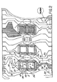
- the system shown in Figure 1 com - took six peripheral electrodes 1, 2, 3, 4, 5 and 6 and 7 a seventh placed at the center. These electrodes are constituted for example by a layer of indium oxide doped with tin, or tin oxide doped with antimony. It further comprises current leads respectively 11 to 17 which connect the electrodes to connection pads 21 to 27 respectively. These pads can be distributed on either side of the device, as illustrated, or can all be brought back from one same side.
- each current supply comprises a throttling zone, respectively 31 to 37, including those of the peripheral electrodes 1 to 6.
- the throttling of the current supply 17 specific to the central electrode 7, is, in the illustrated case, located between the peripheral electrodes 1 and 2.
- the current leads then have a flared area which terminates on the long side of the electrodes. In this way, the electrode is supplied in a substantially uniform manner over its entire length. The only uniformity defect which may still remain results from the voltage drop across the width of the electrode, a drop which is negligible.
- the width and the length of the current leads between the studs 21-27 and the throttles 31-37 are adjusted so that the voltage drops between said studs and said throttles are the same for all the current leads 11 to 17. Thus is ensures uniformity of display across all electrodes, including the center electrode.
- FIGS. 2 and 3 which represent a variant in which the electrodes and the current leads are formed by the same transparent conductive material deposited in a thin layer on the entire wall, l 'isolation between different current leads being provided by grooves etched in this layer.
- Figure 2 shows the system in top view and Figure 3 two sections, on the one hand in the vicinity of the electrode 1 (Fig. A) and on the other hand in the region of the throttle 37 located between the electrodes 1 and 2 (Fig. B).
- the system comprises a wall covered by a uniform layer 44 of a transparent conductive material (for example indium oxide doped with tin), in which grooves 40 are etched to isolate the leads from current between them, to also isolate the connection pads and to form the constrictions.
- This layer 44 is covered with an insulating layer 46 (for example made of silica), except at the locations of the electrodes, which are then in contact with an electrolyte 48.
- the display occurs for example by deposition and redissolution of a metallic layer 50 (including money).
- the current supply is separated from said electrodes by two grooves 40 and the gap is covered with insulating material.
- the interval between the electrodes 1 and 2 may be of the order of 400 to 500 fL m and the grooves may have a width of the order of 50 fL m.
- the advantage of the embodiment of Figures 2 and 3 is to lead to excellent uniformity of the appearance presented by the display, due to the uniformity of the structure of the wall offered to the eyes of the observer.
- the central segment is supplied by a current supply coming from the top for the first system, coming from the bottom for the second, and so on alternately.
- the central electrode is in fact also in contact with a symmetrical conductive zone of the current supply zone, this symmetrical zone not participating in the supply of the segment but being nevertheless produced to obtain uniformity appearance of the cell.
Landscapes
- Physics & Mathematics (AREA)
- Nonlinear Science (AREA)
- General Physics & Mathematics (AREA)
- Optics & Photonics (AREA)
- Engineering & Computer Science (AREA)
- Theoretical Computer Science (AREA)
- Devices For Indicating Variable Information By Combining Individual Elements (AREA)
- Electrochromic Elements, Electrophoresis, Or Variable Reflection Or Absorption Elements (AREA)
Applications Claiming Priority (2)
| Application Number | Priority Date | Filing Date | Title |
|---|---|---|---|
| FR7916740A FR2460518A1 (fr) | 1979-06-28 | 1979-06-28 | Systeme d'electrodes de commande pour afficheur numerique a sept segments |
| FR7916740 | 1979-06-28 |
Publications (2)
| Publication Number | Publication Date |
|---|---|
| EP0021992A1 EP0021992A1 (fr) | 1981-01-07 |
| EP0021992B1 true EP0021992B1 (fr) | 1984-05-16 |
Family
ID=9227244
Family Applications (1)
| Application Number | Title | Priority Date | Filing Date |
|---|---|---|---|
| EP80400896A Expired EP0021992B1 (fr) | 1979-06-28 | 1980-06-18 | Système d'électrodes de commande pour afficheur numérique à sept segments |
Country Status (4)
| Country | Link |
|---|---|
| US (1) | US4333710A (OSRAM) |
| EP (1) | EP0021992B1 (OSRAM) |
| DE (1) | DE3067824D1 (OSRAM) |
| FR (1) | FR2460518A1 (OSRAM) |
Families Citing this family (4)
| Publication number | Priority date | Publication date | Assignee | Title |
|---|---|---|---|---|
| JPS5776589A (en) * | 1980-10-30 | 1982-05-13 | Sharp Kk | Electrochromatic indicator |
| CA2220519A1 (en) * | 1995-05-09 | 1996-11-21 | James P. Coleman | Conductive font |
| JPH103987A (ja) * | 1996-06-12 | 1998-01-06 | Futaba Corp | 有機エレクトロルミネッセンス素子 |
| DE19825371A1 (de) * | 1998-06-06 | 1999-12-09 | Bayer Ag | Elektrochrome Anzeigevorrichtung mit isolierten Zuleitungen |
Family Cites Families (10)
| Publication number | Priority date | Publication date | Assignee | Title |
|---|---|---|---|---|
| US3702723A (en) * | 1971-04-23 | 1972-11-14 | American Micro Syst | Segmented master character for electronic display apparatus |
| US4086003A (en) * | 1974-07-15 | 1978-04-25 | Kabushiki Kaisha Suwa Seikosha | Electrochromic display cell |
| JPS5231724U (OSRAM) * | 1975-08-29 | 1977-03-05 | ||
| JPS5810753B2 (ja) * | 1975-09-29 | 1983-02-26 | シャープ株式会社 | エレクトロクロミツクヒヨウジソシノ セイゾウホウホウ |
| GB1559678A (en) * | 1975-10-31 | 1980-01-23 | Ici Ltd | Display device |
| DE2725265A1 (de) * | 1976-06-04 | 1977-12-08 | Tokyo Shibaura Electric Co | Halbleiter-leuchtanzeigevorrichtung |
| JPS5310297A (en) * | 1976-07-16 | 1978-01-30 | Sharp Corp | Electrochromic display device |
| JPS5347294A (en) * | 1976-10-12 | 1978-04-27 | Seiko Instr & Electronics Ltd | Electrochemical light emitting display device |
| US4128316A (en) * | 1977-06-15 | 1978-12-05 | Timex Corporation | Thin electrochromic display |
| FR2407746A1 (fr) * | 1977-11-07 | 1979-06-01 | Commissariat Energie Atomique | Electrode pour cellule d'electrolyse, notamment pour cellule d'affichage electrolytique et son procede de fabrication |
-
1979
- 1979-06-28 FR FR7916740A patent/FR2460518A1/fr active Granted
-
1980
- 1980-06-18 EP EP80400896A patent/EP0021992B1/fr not_active Expired
- 1980-06-18 DE DE8080400896T patent/DE3067824D1/de not_active Expired
- 1980-06-23 US US06/161,921 patent/US4333710A/en not_active Expired - Lifetime
Also Published As
| Publication number | Publication date |
|---|---|
| FR2460518B1 (OSRAM) | 1982-08-27 |
| EP0021992A1 (fr) | 1981-01-07 |
| US4333710A (en) | 1982-06-08 |
| FR2460518A1 (fr) | 1981-01-23 |
| DE3067824D1 (en) | 1984-06-20 |
Similar Documents
| Publication | Publication Date | Title |
|---|---|---|
| EP0267824B1 (fr) | Ecran de visualisation électrooptique à transistors de commande et procédé de réalisation | |
| FR2585167A1 (fr) | Structures conductrices redondantes pour affichages a cristaux liquides commandes par des transistors a effet de champ en couche mince | |
| FR2768239A1 (fr) | Afficheur a cristaux liquides et procede de fabrication de celui-ci | |
| EP0317910A1 (fr) | Cellule d'affichage à cristal liquide comprenant un réflecteur-diffuseur et au plus un polariseur | |
| WO1990011594A1 (fr) | Tete magnetique de lecture a magnetoresistance pour enregistrement perpendiculaire et procede de realisation d'une telle tete | |
| FR2754917A1 (fr) | Afficheur a cristal liquide et son procede de fabrication | |
| FR2604021A1 (fr) | Procede de realisation de tetes magnetiques en couches minces et a structure planaire et tete obtenue par ce procede | |
| FR2760288A1 (fr) | Structure d'un afficheur a cristaux liquides et son procede de fabrication | |
| FR2780521A1 (fr) | Procede de fabrication d'une partie de plages d'un afficheur a cristal liquide, et structure d'afficheur presentant ladite partie | |
| EP0599174B1 (fr) | Cellule de mesure micro-usinée | |
| FR2564225A1 (fr) | Dispositif d'affichage avec axe incline du disque | |
| EP0021992B1 (fr) | Système d'électrodes de commande pour afficheur numérique à sept segments | |
| EP3465724A1 (fr) | Membrane mems à ligne de transmission intégrée | |
| EP0564337B1 (fr) | Ecran d'affichage à masque optique et procédé de réalisation de cet écran | |
| EP0041890B1 (fr) | Elément à conduction non linéaire, et dispositif à commutation, de visualisation notamment, incorporant un tel élément | |
| EP0217844B1 (fr) | Procede de fabrication d'un ecran d'affichage a cristaux liquides et a reseau de diodes | |
| EP0607350B1 (fr) | Ecran Plat à Cristaux Liquides | |
| WO2004051356A1 (fr) | Structure de matrice active pour ecran de visualisation et ecran comportant une telle matrice | |
| CH620523A5 (en) | Electrochromic display cell | |
| EP0266252B1 (fr) | Ecran de visualisation électrooptique à transistors de commande et procédé de réalisation | |
| EP0006811A2 (fr) | Cellule d'affichage électrolytique à dépôt métallique et procédé pour éviter un appauvrissement en métal de certaines zones de la contre-électrode d'une telle cellule | |
| EP0145651A2 (fr) | Dispositif pour former des signaux caractéristiques de la position d'un point déterminé sur une surface | |
| EP1565807B1 (fr) | Dispositif d'affichage dédié à détection de proximité | |
| FR2602362A1 (fr) | Dispositif d'affichage matriciel comprenant deux paquets d'electrodes lignes et deux electrodes colonnes par element image et son procede de commande | |
| FR2499741A1 (fr) | Perfectionnements apportes aux dispositifs afficheurs a cristal liquide |
Legal Events
| Date | Code | Title | Description |
|---|---|---|---|
| PUAI | Public reference made under article 153(3) epc to a published international application that has entered the european phase |
Free format text: ORIGINAL CODE: 0009012 |
|
| AK | Designated contracting states |
Designated state(s): CH DE GB IT NL |
|
| 17P | Request for examination filed |
Effective date: 19810606 |
|
| ITF | It: translation for a ep patent filed | ||
| GRAA | (expected) grant |
Free format text: ORIGINAL CODE: 0009210 |
|
| AK | Designated contracting states |
Designated state(s): CH DE GB IT LI NL |
|
| PGFP | Annual fee paid to national office [announced via postgrant information from national office to epo] |
Ref country code: DE Payment date: 19840526 Year of fee payment: 5 |
|
| PGFP | Annual fee paid to national office [announced via postgrant information from national office to epo] |
Ref country code: CH Payment date: 19840606 Year of fee payment: 5 |
|
| REF | Corresponds to: |
Ref document number: 3067824 Country of ref document: DE Date of ref document: 19840620 |
|
| PGFP | Annual fee paid to national office [announced via postgrant information from national office to epo] |
Ref country code: NL Payment date: 19840630 Year of fee payment: 5 |
|
| PLBE | No opposition filed within time limit |
Free format text: ORIGINAL CODE: 0009261 |
|
| STAA | Information on the status of an ep patent application or granted ep patent |
Free format text: STATUS: NO OPPOSITION FILED WITHIN TIME LIMIT |
|
| 26N | No opposition filed | ||
| PG25 | Lapsed in a contracting state [announced via postgrant information from national office to epo] |
Ref country code: LI Effective date: 19850630 Ref country code: CH Effective date: 19850630 |
|
| PG25 | Lapsed in a contracting state [announced via postgrant information from national office to epo] |
Ref country code: NL Effective date: 19860101 |
|
| GBPC | Gb: european patent ceased through non-payment of renewal fee | ||
| REG | Reference to a national code |
Ref country code: CH Ref legal event code: PL |
|
| PG25 | Lapsed in a contracting state [announced via postgrant information from national office to epo] |
Ref country code: DE Effective date: 19860301 |
|
| NLV4 | Nl: lapsed or anulled due to non-payment of the annual fee | ||
| PG25 | Lapsed in a contracting state [announced via postgrant information from national office to epo] |
Ref country code: GB Effective date: 19881118 |