EP0021992B1 - Control electrodes system for a seven digits indicator - Google Patents
Control electrodes system for a seven digits indicator Download PDFInfo
- Publication number
- EP0021992B1 EP0021992B1 EP80400896A EP80400896A EP0021992B1 EP 0021992 B1 EP0021992 B1 EP 0021992B1 EP 80400896 A EP80400896 A EP 80400896A EP 80400896 A EP80400896 A EP 80400896A EP 0021992 B1 EP0021992 B1 EP 0021992B1
- Authority
- EP
- European Patent Office
- Prior art keywords
- electrodes
- electrode
- layer
- electrical leads
- current
- Prior art date
- Legal status (The legal status is an assumption and is not a legal conclusion. Google has not performed a legal analysis and makes no representation as to the accuracy of the status listed.)
- Expired
Links
Images

Classifications
-
- G—PHYSICS
- G02—OPTICS
- G02F—OPTICAL DEVICES OR ARRANGEMENTS FOR THE CONTROL OF LIGHT BY MODIFICATION OF THE OPTICAL PROPERTIES OF THE MEDIA OF THE ELEMENTS INVOLVED THEREIN; NON-LINEAR OPTICS; FREQUENCY-CHANGING OF LIGHT; OPTICAL LOGIC ELEMENTS; OPTICAL ANALOGUE/DIGITAL CONVERTERS
- G02F1/00—Devices or arrangements for the control of the intensity, colour, phase, polarisation or direction of light arriving from an independent light source, e.g. switching, gating or modulating; Non-linear optics
- G02F1/01—Devices or arrangements for the control of the intensity, colour, phase, polarisation or direction of light arriving from an independent light source, e.g. switching, gating or modulating; Non-linear optics for the control of the intensity, phase, polarisation or colour
- G02F1/0102—Constructional details, not otherwise provided for in this subclass
-
- G—PHYSICS
- G02—OPTICS
- G02F—OPTICAL DEVICES OR ARRANGEMENTS FOR THE CONTROL OF LIGHT BY MODIFICATION OF THE OPTICAL PROPERTIES OF THE MEDIA OF THE ELEMENTS INVOLVED THEREIN; NON-LINEAR OPTICS; FREQUENCY-CHANGING OF LIGHT; OPTICAL LOGIC ELEMENTS; OPTICAL ANALOGUE/DIGITAL CONVERTERS
- G02F1/00—Devices or arrangements for the control of the intensity, colour, phase, polarisation or direction of light arriving from an independent light source, e.g. switching, gating or modulating; Non-linear optics
- G02F1/01—Devices or arrangements for the control of the intensity, colour, phase, polarisation or direction of light arriving from an independent light source, e.g. switching, gating or modulating; Non-linear optics for the control of the intensity, phase, polarisation or colour
- G02F1/15—Devices or arrangements for the control of the intensity, colour, phase, polarisation or direction of light arriving from an independent light source, e.g. switching, gating or modulating; Non-linear optics for the control of the intensity, phase, polarisation or colour based on an electrochromic effect
- G02F1/153—Constructional details
- G02F1/155—Electrodes
-
- G—PHYSICS
- G09—EDUCATION; CRYPTOGRAPHY; DISPLAY; ADVERTISING; SEALS
- G09F—DISPLAYING; ADVERTISING; SIGNS; LABELS OR NAME-PLATES; SEALS
- G09F9/00—Indicating arrangements for variable information in which the information is built-up on a support by selection or combination of individual elements
- G09F9/30—Indicating arrangements for variable information in which the information is built-up on a support by selection or combination of individual elements in which the desired character or characters are formed by combining individual elements
- G09F9/302—Indicating arrangements for variable information in which the information is built-up on a support by selection or combination of individual elements in which the desired character or characters are formed by combining individual elements characterised by the form or geometrical disposition of the individual elements
Definitions
- the present invention relates to an electrode system for an electrolytic display with seven segments according to the preamble of claim 1, such a system is known from document DE-A-2 731 718. It finds an application in the production of organs display (watches, dashboards, measuring devices, etc.).
- a seven segment electrolytic display cell includes a counter electrode opposite which are arranged seven transparent electrodes distributed in six peripheral electrodes and a central electrode. Each electrode is supplied with current by a current supply itself connected to a connection pad allowing a connection with suitable supply members. Between the electrodes and the counter-electrode is inserted an electrolyte which is able, under the effect of the current flow, to modify the appearance of the electrodes, in particular by the deposition then by the dissolution of a layer of metal.
- electrolytic cells pose specific problems that are not found in other types of cells, liquid crystal or electrochromic material for example. Indeed, in the electrolytic display, it is imperative to ensure that the potential applied to the excited electrodes has good uniformity, otherwise the contrast of the display obtained does not have the required uniformity. This is due to the electrochemical nature of the reactions that occur on the electrodes. This constraint does not exist in liquid crystal cells where the current is approximately 1,000 times weaker than in electrolytic cells (some fL A / cm z against some mA / cm z ), this current being elsewhere or current leakage and not control current. It also does not exist in electrochromic devices (at W0 3 for example) for which the appearance or disappearance of a coloration is less critical.
- each segment will be well supplied by one of its long sides, but in an non-equipotential manner, because the leads are narrow bands; and anyway, this technique valid for semiconductors cannot be transposed to electrolytic devices where the layers in play are very thin and resistive.
- the present invention as claimed is precisely intended to remedy these drawbacks by proposing a system which makes it possible to simultaneously solve the three difficulties mentioned above.
- This goal is achieved by feeding the seven electrodes in the same way.
- the presence of a central electrode requires that the current supply specific to this electrode passes between two peripheral electrodes, which leads to a constriction for the current supply.
- this constriction is therefore reproduced on the current leads specific to the six peripheral electrodes, which obviously is not achieved in the prior art where the advantage is taken of the ease of access of the peripheral electrodes to supply these by current leads of simple forms.
- each electrode is supplied ie along the whole of one of its long sides.
- the present invention relates to an electrode system for an electrolytic display with seven segments, comprising on one wall seven electrodes formed by a first transparent thin conductive layer in the form of a segment having two long sides, these electrodes being distributed in six peripheral electrodes and a central electrode, each electrode being connected to a second thin conductive layer deposited on said wall and forming a current supply, each lead being connected to a connection pad, characterized in that each current lead comprises a throttle zone producing the same voltage drops between said pads and said electrodes and followed by a flaring zone of the current lead terminating on the whole of one of the long sides of one of the electrodes and constituting an equipotential line along this long side, the constriction proper to the current supply assigned to the central electrode being located between two adjacent peripheral electrodes, one of which is parallel to the central electrode.
- the first layer constituting the electrodes and the second layer constituting the current leads consist of a single layer of a single transparent conductive material, the current leads being covered with an insulating material.
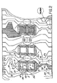
- the system shown in Figure 1 com - took six peripheral electrodes 1, 2, 3, 4, 5 and 6 and 7 a seventh placed at the center. These electrodes are constituted for example by a layer of indium oxide doped with tin, or tin oxide doped with antimony. It further comprises current leads respectively 11 to 17 which connect the electrodes to connection pads 21 to 27 respectively. These pads can be distributed on either side of the device, as illustrated, or can all be brought back from one same side.
- each current supply comprises a throttling zone, respectively 31 to 37, including those of the peripheral electrodes 1 to 6.
- the throttling of the current supply 17 specific to the central electrode 7, is, in the illustrated case, located between the peripheral electrodes 1 and 2.
- the current leads then have a flared area which terminates on the long side of the electrodes. In this way, the electrode is supplied in a substantially uniform manner over its entire length. The only uniformity defect which may still remain results from the voltage drop across the width of the electrode, a drop which is negligible.
- the width and the length of the current leads between the studs 21-27 and the throttles 31-37 are adjusted so that the voltage drops between said studs and said throttles are the same for all the current leads 11 to 17. Thus is ensures uniformity of display across all electrodes, including the center electrode.
- FIGS. 2 and 3 which represent a variant in which the electrodes and the current leads are formed by the same transparent conductive material deposited in a thin layer on the entire wall, l 'isolation between different current leads being provided by grooves etched in this layer.
- Figure 2 shows the system in top view and Figure 3 two sections, on the one hand in the vicinity of the electrode 1 (Fig. A) and on the other hand in the region of the throttle 37 located between the electrodes 1 and 2 (Fig. B).
- the system comprises a wall covered by a uniform layer 44 of a transparent conductive material (for example indium oxide doped with tin), in which grooves 40 are etched to isolate the leads from current between them, to also isolate the connection pads and to form the constrictions.
- This layer 44 is covered with an insulating layer 46 (for example made of silica), except at the locations of the electrodes, which are then in contact with an electrolyte 48.
- the display occurs for example by deposition and redissolution of a metallic layer 50 (including money).
- the current supply is separated from said electrodes by two grooves 40 and the gap is covered with insulating material.
- the interval between the electrodes 1 and 2 may be of the order of 400 to 500 fL m and the grooves may have a width of the order of 50 fL m.
- the advantage of the embodiment of Figures 2 and 3 is to lead to excellent uniformity of the appearance presented by the display, due to the uniformity of the structure of the wall offered to the eyes of the observer.
- the central segment is supplied by a current supply coming from the top for the first system, coming from the bottom for the second, and so on alternately.
- the central electrode is in fact also in contact with a symmetrical conductive zone of the current supply zone, this symmetrical zone not participating in the supply of the segment but being nevertheless produced to obtain uniformity appearance of the cell.
Description
La présente invention a pour objet un système d'électrodes pour afficheur électrolytique à sept segments selon le préambule de la revendication 1, un tel système est connu du document DE-A-2 731 718. Elle trouve une application dans la réalisation d'organes d'affichage (montres, tableaux de bord, appareils de mesure, etc...).The present invention relates to an electrode system for an electrolytic display with seven segments according to the preamble of claim 1, such a system is known from document DE-A-2 731 718. It finds an application in the production of organs display (watches, dashboards, measuring devices, etc.).
Une cellule d'affichage électrolytique à sept segments comprend une contre-électrode en regard de laquelle sont disposées sept électrodes transparentes réparties en six électrodes périphériques et une électrode centrale. Chaque électrode est alimentée en courant par une amenée de courant elle-même reliée à un plot de connexion permettant une liaison avec des organes d'alimentation appropriés. Entre les électrodes et la contre-électrode est inséré un électrolyte qui est apte, sous l'effet du passage du courant, à modifier l'aspect des électrodes, notamment par le dépôt puis par la dissolution d'une couche de métal.A seven segment electrolytic display cell includes a counter electrode opposite which are arranged seven transparent electrodes distributed in six peripheral electrodes and a central electrode. Each electrode is supplied with current by a current supply itself connected to a connection pad allowing a connection with suitable supply members. Between the electrodes and the counter-electrode is inserted an electrolyte which is able, under the effect of the current flow, to modify the appearance of the electrodes, in particular by the deposition then by the dissolution of a layer of metal.
La commande des cellules électrolytiques pose des problèmes spécifiques qu'on ne retrouve pas dans les autres types de cellules, à cristaux liquides ou à matériau électrochrome par exemple. En effet, dans l'affichage électrolytique, il est impératif de faire en sorte que le potentiel appliqué aux électrodes excitées présente une bonne uniformité, sinon le contraste de l'affichage obtenu ne présente pas l'uniformité requise. Cela est dû à la nature électrochimique des réactions qui se produisent sur les électrodes. Cette contrainte n'existe pas dans les cellules à cristaux liquides où le courant est environ 1 000 fois plus faible que dans le cellules électrolytiques (quelques fLA/cmz contre quelques mA/cmz), ce courant étant d'ailleurs ou courant de fuite et non un courant de commande. Elle n'existe pas non plus dans les dispositifs électrochromes (à W03 par exemple) pour lesquels l'apparition ou la disparition d'une coloration sont moins critiques.The control of electrolytic cells poses specific problems that are not found in other types of cells, liquid crystal or electrochromic material for example. Indeed, in the electrolytic display, it is imperative to ensure that the potential applied to the excited electrodes has good uniformity, otherwise the contrast of the display obtained does not have the required uniformity. This is due to the electrochemical nature of the reactions that occur on the electrodes. This constraint does not exist in liquid crystal cells where the current is approximately 1,000 times weaker than in electrolytic cells (some fL A / cm z against some mA / cm z ), this current being elsewhere or current leakage and not control current. It also does not exist in electrochromic devices (at W0 3 for example) for which the appearance or disappearance of a coloration is less critical.
C'est la raison pour laquelle les systèmes d'électrodes connus pour les cellules à cristaux liquides ou à couche électrochrome ne donnent pas satisfaction si on les adopte pour les cellules électrolytiques.This is the reason why the known electrode systems for liquid crystal or electrochromic layer cells are not satisfactory if they are adopted for electrolytic cells.
Le problème de l'uniformité du contraste dans les cellules électrolytiques est d'autant plus ardu à résoudre que les amenées de courant et les électrodes sont constituées par des couches minces d'oxyde conducteur qui présentent, du fait de leur minceur, une résistivité non négligeable. Ce problème recouvre en fait trois difficultés: a) obtenir l'égalité de la chute de tension le long de l'amenée de courant entre le plot de connexion et l'électrode, b) assurer une uniformité de potentiel sur la totalité de la surface de chaque électrode, c) résoudre les deux points précédents pour tous les segments, y compris les segment central, lequel est d'accès difficile puisqu'entouré par les six segments périphériques.The problem of the uniformity of the contrast in the electrolytic cells is all the more difficult to solve since the current leads and the electrodes are constituted by thin layers of conductive oxide which have, because of their thinness, a non resistivity. negligible. This problem in fact covers three difficulties: a) obtaining the equality of the voltage drop along the current supply between the connection pad and the electrode, b) ensuring a uniformity of potential over the entire surface of each electrode, c) solve the two previous points for all the segments, including the central segment, which is difficult to access since it is surrounded by the six peripheral segments.
Si l'on utilise la technique décrite dans "Patent Abstract of Japan", vol. 2, n° 82, 30.6.1978, page 3512 E 78, Kokai Nr 53-47294, on obtient bien une égalité de la chute de tension mais le segment central est le siège d'un gradient de potentiel puisqu'il est alimenté par l'un de ses petits côtés. De même avec la technique du document DE-A-2 731 718. Si l'on utilise un dispositif du type de celui décrit par exemple dans le document US-A-3 702 723, la chute de tension ne nera pas la même sur toutes les amenées de courant entre le plot et l'électrode et les segments ne présenteront pas tous le même aspect. Si l'on utilise la disposition du document DE-A-2 725 265 valable pour les dispositifs à semiconducteurs, chaque segment sera bien alimenté par un de ses grands côtés, mais de manière non équipotentielle, car les amenées sont des bandes étroites; et le toute façon, cette technique valable pour les semiconducteurs n'est pas transposable aux dispositifs électrolytiques où les couches en jeu sont très minces et résistives.If the technique described in "Patent Abstract of Japan", vol. 2, n ° 82, 30.6.1978, page 3512 E 78, Kokai Nr 53-47294, we get a good voltage drop equality but the central segment is the seat of a potential gradient since it is powered by one of its short sides. Similarly with the technique of document DE-A-2 731 718. If a device of the type described for example in document US-A-3 702 723 is used, the voltage drop will not be the same on all the current leads between the pad and the electrode and the segments will not all have the same appearance. If one uses the provision of document DE-A-2 725 265 valid for semiconductor devices, each segment will be well supplied by one of its long sides, but in an non-equipotential manner, because the leads are narrow bands; and anyway, this technique valid for semiconductors cannot be transposed to electrolytic devices where the layers in play are very thin and resistive.
La présente invention telle qu'elle est revendiquée a justement pour but de remédier à ces inconvénients en proposant un système qui permet de résoudre simultanément les trois difficultés mentionnées plus haut. Ce but est atteint en alimentant les sept électrodes de la même manière. La présence d'une électrode centrale nécessite que l'amenée de courant propre à cette électrode passe entre deux électrodes périphériques, ce qui conduit à un étranglement pour l'amenée de courant. Selon l'invention, cet étranglement est donc reproduit sur les amenées de courant propres aux six électrodes périphériques, ce qui évidemment n'est pas réalisé dans l'art antérieur où l'on profite de la facilité d'accès des électrodes périphériques pour alimenter celles-ci par des amenées de courant de formes simples. En outre, pour éviter la chute de tension le long d'un segment, chaque électrode est alimentée ie long de la totalité d'un de ses grands côtés. Ceci nécessite, pour chaque amenée de courant, une zone évasée entre l'étranglement et le segment. De cette manière, les lignes de courant divergent (ou convergent selon le sens du courant) entre l'étranglement et le grand côté de l'électrode, ce grand côté étant alors sensiblement confondu avec une ligne équipotentielle de l'amenée de courant. Naturellement, on s'efforce en outre de donner aux dimensions (largeur et longueur) des amenées de courant entre un plot et l'étranglement associé des valeurs telles que les chutes de tensions soient les mêmes pour toutes les amenées de courant.The present invention as claimed is precisely intended to remedy these drawbacks by proposing a system which makes it possible to simultaneously solve the three difficulties mentioned above. This goal is achieved by feeding the seven electrodes in the same way. The presence of a central electrode requires that the current supply specific to this electrode passes between two peripheral electrodes, which leads to a constriction for the current supply. According to the invention, this constriction is therefore reproduced on the current leads specific to the six peripheral electrodes, which obviously is not achieved in the prior art where the advantage is taken of the ease of access of the peripheral electrodes to supply these by current leads of simple forms. In addition, to avoid the voltage drop along a segment, each electrode is supplied ie along the whole of one of its long sides. This requires, for each current supply, a flared zone between the throttle and the segment. In this way, the current lines diverge (or converge depending on the direction of the current) between the constriction and the long side of the electrode, this long side then being substantially coincident with an equipotential line of the current supply. Naturally, an effort is also made to give the dimensions (width and length) of the current leads between a stud and the associated throttle values such that the voltage drops are the same for all the current leads.
De façon précise, la présente invention a pour objet un système d'électrodes pour afficheur électrolytique à sept segments, comprenant sur une paroi sept électrodes constituées par une première couche conductrice mince transparente en forme de segment ayant deux grands côtés, ces électrodes étant réparties en six électrodes périphériques et une électrode centrale, chaque électrode étant reliée à une seconde couche conductrice mince déposée sur ladite paroi et formant amenée de courant, chaque amenée étant reliée à un plot de connexion, caractérisé en ce que chaque amenée de courant comprend une zone d'étranglement réalisant les mêmes chutes de tensions entre lesdits plots et lesdites électrodes et suivie d'une zone d'évasément de l'amenée de courant aboutissant sur la totalité d'un des grands côtés d'une des électrodes et constituant une ligne équipotentielle lelong de ce grand côté, l'étranglement propre à l'amenée de courant affectée à l'électrode centrale étant situé entre deux électrodes périphériques adjacentes, dont l'une est parallèle à l'électrode centrale.Specifically, the present invention relates to an electrode system for an electrolytic display with seven segments, comprising on one wall seven electrodes formed by a first transparent thin conductive layer in the form of a segment having two long sides, these electrodes being distributed in six peripheral electrodes and a central electrode, each electrode being connected to a second thin conductive layer deposited on said wall and forming a current supply, each lead being connected to a connection pad, characterized in that each current lead comprises a throttle zone producing the same voltage drops between said pads and said electrodes and followed by a flaring zone of the current lead terminating on the whole of one of the long sides of one of the electrodes and constituting an equipotential line along this long side, the constriction proper to the current supply assigned to the central electrode being located between two adjacent peripheral electrodes, one of which is parallel to the central electrode.
De préférence, la première couche constituant les électrodes et la seconde couche constituant les amenées de courant sont constituées par une seule couche d'un matériau conducteur transparent unique, les amenées de courant étant recouvertes d'un matériau isolant.Preferably, the first layer constituting the electrodes and the second layer constituting the current leads consist of a single layer of a single transparent conductive material, the current leads being covered with an insulating material.
De toute façon, les charactéristiques et avantages de la présente invention apparaîtront mieux après la description qui suit d'exemples de réalisation. Cette description se réfère à des dessins annexés sur lesquels:
- - la figure 1 représente schématiquement un système d'électrodes selon l'invention,
- -la figure 2 illustre un mode particulier de réalisation d'un afficheur électrolytique conforme à l'invention,
- - la figure 3 représente deux détails vus en coupe de l'afficheur de la figure précédente.
- FIG. 1 diagrammatically represents an electrode system according to the invention,
- FIG. 2 illustrates a particular embodiment of an electrolytic display according to the invention,
- - Figure 3 shows two details seen in section of the display of the previous figure.
Le système représenté sur la figure 1 com- prend six électrodes périphériques 1, 2, 3, 4, 5 et 6 et une septième 7 placée au centre. Ces électrodes sont constituées par exemple par une couche d'oxyde d'indium dopé à l'étain, ou d'oxyde d'étain dopé à l'antimoine. Il comprend en outre des amenées de courant respectivement 11 à 17 qui relient les électrodes à des plots de connexion respectivement 21 à 27. Ces plots peuvent être répartis de part et d'autre du dispositif, comme illustré, ou être tous ramenés d'un même côté.The system shown in Figure 1 com - took six
Conformément à l'invention, chaque amenée de courant comprend une zone d'étranglement, respectivement 31 à 37, y compris celles des électrodes périphériques 1 à 6. L'étranglement de l'amenée de courant 17 propre à l'électrode centrale 7, est, dans le cas illustré, situé entre les électrodes périphériques 1 et 2. Les amenées de courant présentent ensuite en zone évasée qui aboutit sur le grand côté des électrodes. De cette manière, l'électrode est alimentée de manière sensiblement uniforme sur toute sa longueur. Le seul défaut d'uniformité pouvant encore subsister résulte de la chute de tension dans le sens de la largeur de l'électrode, chute qui est négligeable. La largeur et la longueur des amenées de courant entre les plots 21-27 et les étranglements 31-37 sont ajustées pour que les chutes de tensions entre lesdits plots et lesdits étranglements soient les mêmes pour toutes les amenées de courant 11 à 17. Ainsi est assurée l'uniformité de l'affichage sur la totalité des électrodes, y compris l'électrode centrale.According to the invention, each current supply comprises a throttling zone, respectively 31 to 37, including those of the peripheral electrodes 1 to 6. The throttling of the
La figure 1 est un schéma de principe. Dans la pratique, on peut constituer le système comme illustré sur les figures 2 et 3 qui représentent une variante dans laquelle les électrodes et les amenées de courant sont constituées par un même matériau conducteur transparent déposé en couche mince sur la totalité de la paroi, l'isolement entre différentes amenées de courant étant assuré par des sillons gravés dans cette couche. La figure 2 représente le système en vue de dessus et la figure 3 deux coupes, d'une part au voisinage de l'électrode 1 (Fig. a) et d'autre part dans la zone de l'étranglement 37 situé entre les électrodes 1 et 2 (Fig. b). Tel qu'illustré, le système comprend une paroi recouverte par une couche uniforme 44 d'un matériau conducteur transparent (par exemple d'oxyde d'indium dopé à l'étain), dans laquelle des sillons 40 sont gravés pour isoler les amenées de courant entre elles, pour isoler également les plots de connexion et pour former les étranglements. Cette couche 44 est recouverte d'une couche isolante 46 (par exemple en silice), sauf aux endroits des électrodes, lesquelles sont alors en contact avec un électrolyte 48. L'affichage se produit par exemple par dépôt et redissolution d'une couche métallique 50 (notamment d'argent). Dans la zone située entre les électrodes 1 et 2 (Fig. 3b), l'amenée de courant est séparée desdites électrodes par deux sillons 40 et l'intervalle est recouvert de matière isolante.Figure 1 is a block diagram. In practice, the system can be constituted as illustrated in FIGS. 2 and 3 which represent a variant in which the electrodes and the current leads are formed by the same transparent conductive material deposited in a thin layer on the entire wall, l 'isolation between different current leads being provided by grooves etched in this layer. Figure 2 shows the system in top view and Figure 3 two sections, on the one hand in the vicinity of the electrode 1 (Fig. A) and on the other hand in the region of the
A titre explicatif, l'intervalle entre les électrodes 1 et 2, peut être de l'ordre de 400 à 500 fLm et les sillons peuvent présenter une largeur de l'ordre de 50 fLm.By way of explanation, the interval between the
L'intérêt du mode de réalisation des figures 2 et 3 est de conduire à une excellente uniformité de l'aspect présenté par l'afficheur, du fait de l'uniformité de structure de la paroi offerte aux regards de l'observateur.The advantage of the embodiment of Figures 2 and 3 is to lead to excellent uniformity of the appearance presented by the display, due to the uniformity of the structure of the wall offered to the eyes of the observer.
Dans l'exemple illustré sur la figure 2, on observera que le segment central est alimenté par une amenée de courant venant du haut pour le premier système, venant du bas pour le second, et ainsi de suite alternativement. Dans chaque système, l'électrode centrale est en fait en contact également avec une zone conductrice symétrique de la zone d'amenée de courant, cette zone symétrique ne participant pas à l'alimentation du segment mais étant tout de même réalisée pour obtenir une uniformité d'aspect de la cellule. De même, il existe des îlots de matière conductrice qui ne jouent aucun rôle, si ce n'est de remplir la surface visible.In the example illustrated in FIG. 2, it will be observed that the central segment is supplied by a current supply coming from the top for the first system, coming from the bottom for the second, and so on alternately. In each system, the central electrode is in fact also in contact with a symmetrical conductive zone of the current supply zone, this symmetrical zone not participating in the supply of the segment but being nevertheless produced to obtain uniformity appearance of the cell. Likewise, there are islands of conductive material which play no role, except to fill the visible surface.
Claims (3)
Applications Claiming Priority (2)
| Application Number | Priority Date | Filing Date | Title |
|---|---|---|---|
| FR7916740 | 1979-06-28 | ||
| FR7916740A FR2460518A1 (en) | 1979-06-28 | 1979-06-28 | CONTROL ELECTRODE SYSTEM FOR SEVEN SEGMENT DIGITAL DISPLAY |
Publications (2)
| Publication Number | Publication Date |
|---|---|
| EP0021992A1 EP0021992A1 (en) | 1981-01-07 |
| EP0021992B1 true EP0021992B1 (en) | 1984-05-16 |
Family
ID=9227244
Family Applications (1)
| Application Number | Title | Priority Date | Filing Date |
|---|---|---|---|
| EP80400896A Expired EP0021992B1 (en) | 1979-06-28 | 1980-06-18 | Control electrodes system for a seven digits indicator |
Country Status (4)
| Country | Link |
|---|---|
| US (1) | US4333710A (en) |
| EP (1) | EP0021992B1 (en) |
| DE (1) | DE3067824D1 (en) |
| FR (1) | FR2460518A1 (en) |
Families Citing this family (4)
| Publication number | Priority date | Publication date | Assignee | Title |
|---|---|---|---|---|
| JPS5776589A (en) * | 1980-10-30 | 1982-05-13 | Sharp Kk | Electrochromatic indicator |
| EP0871949A2 (en) * | 1995-05-09 | 1998-10-21 | Monsanto Company | Conductive font |
| JPH103987A (en) * | 1996-06-12 | 1998-01-06 | Futaba Corp | Organic electroluminescence element |
| DE19825371A1 (en) * | 1998-06-06 | 1999-12-09 | Bayer Ag | Electrochromic display device with insulated leads |
Family Cites Families (10)
| Publication number | Priority date | Publication date | Assignee | Title |
|---|---|---|---|---|
| US3702723A (en) * | 1971-04-23 | 1972-11-14 | American Micro Syst | Segmented master character for electronic display apparatus |
| US4086003A (en) * | 1974-07-15 | 1978-04-25 | Kabushiki Kaisha Suwa Seikosha | Electrochromic display cell |
| JPS5231724U (en) * | 1975-08-29 | 1977-03-05 | ||
| JPS5810753B2 (en) * | 1975-09-29 | 1983-02-26 | シャープ株式会社 | Electrochromic Hiyoji Soshino Seizou Hohou |
| GB1559678A (en) * | 1975-10-31 | 1980-01-23 | Ici Ltd | Display device |
| DE2725265A1 (en) * | 1976-06-04 | 1977-12-08 | Tokyo Shibaura Electric Co | SEMI-CONDUCTOR LIGHT DISPLAY DEVICE |
| JPS5310297A (en) * | 1976-07-16 | 1978-01-30 | Sharp Corp | Electrochromic display device |
| JPS5347294A (en) * | 1976-10-12 | 1978-04-27 | Seiko Instr & Electronics Ltd | Electrochemical light emitting display device |
| US4128316A (en) * | 1977-06-15 | 1978-12-05 | Timex Corporation | Thin electrochromic display |
| FR2407746A1 (en) * | 1977-11-07 | 1979-06-01 | Commissariat Energie Atomique | ELECTRODE FOR ELECTROLYSIS CELL, ESPECIALLY FOR ELECTROLYTIC DISPLAY CELL AND ITS MANUFACTURING PROCESS |
-
1979
- 1979-06-28 FR FR7916740A patent/FR2460518A1/en active Granted
-
1980
- 1980-06-18 EP EP80400896A patent/EP0021992B1/en not_active Expired
- 1980-06-18 DE DE8080400896T patent/DE3067824D1/en not_active Expired
- 1980-06-23 US US06/161,921 patent/US4333710A/en not_active Expired - Lifetime
Also Published As
| Publication number | Publication date |
|---|---|
| DE3067824D1 (en) | 1984-06-20 |
| FR2460518B1 (en) | 1982-08-27 |
| US4333710A (en) | 1982-06-08 |
| EP0021992A1 (en) | 1981-01-07 |
| FR2460518A1 (en) | 1981-01-23 |
Similar Documents
| Publication | Publication Date | Title |
|---|---|---|
| FR2768239A1 (en) | LIQUID CRYSTAL DISPLAY AND METHOD OF MANUFACTURING SAME | |
| FR2623649A1 (en) | LIQUID CRYSTAL DISPLAY CELL | |
| WO1990011594A1 (en) | Magnetic reading head with magnetoresistance for perpendicular recording and method for making such head | |
| FR2754917A1 (en) | LIQUID CRYSTAL DISPLAY AND METHOD FOR MANUFACTURING THE SAME | |
| EP0284495B1 (en) | Magnetic head for reading of very small width tracks and fabrication method | |
| FR2604021A1 (en) | METHOD FOR MAKING THIN FILM MAGNETIC HEADS AND A PLANAR STRUCTURE AND HEAD OBTAINED THEREBY | |
| FR2760288A1 (en) | STRUCTURE OF A LIQUID CRYSTAL DISPLAY AND MANUFACTURING METHOD THEREOF | |
| FR2780521A1 (en) | Grid structure of liquid-crystal display device | |
| FR2564225A1 (en) | DISPLAY DEVICE WITH INCLINE AXIS OF THE DISK | |
| EP0021992B1 (en) | Control electrodes system for a seven digits indicator | |
| EP0246945B1 (en) | Electrooptic screen display and method for its manufacture | |
| FR2698447A1 (en) | Micro-machined measuring cell. | |
| EP0217844B1 (en) | Process for the manufacture of a display screen with liquid crystals and a diode network | |
| EP0564337A1 (en) | Display screen with optical mask and procedure for realization of this screen | |
| EP0041890A1 (en) | Element with non-linear conductivity, and switching circuit, especially for image display with such an element | |
| WO1993007528A1 (en) | Device for enhancing the contrast of a liquid crystal screen and method for producing such device | |
| WO2004051356A1 (en) | Active matrix structure for display screen and screen comprising one such matrix | |
| FR2717304A1 (en) | Electron source with emitting cathodes with microtips. | |
| EP0238405B1 (en) | Method of sequentially controlling a liquid-crystal matrix display device having different optical responses in the ac and dc-fields | |
| EP0359082B1 (en) | Electro-optical cell | |
| FR2551902A1 (en) | NON-LINEAR ELEMENT ADDRESSING DISPLAY SCREEN AND METHOD FOR MANUFACTURING THE SAME | |
| CH620523A5 (en) | Electrochromic display cell | |
| EP0006811A2 (en) | Metal precipitate electrolytic display cell and method to avoid an impoverishment of metal at certain zones of the counter-electrode of such a cell | |
| EP0266252B1 (en) | Transistor-driven electro-optic display and its manufacturing method | |
| EP0209439B1 (en) | Electro-optical display device with liquid crystals |
Legal Events
| Date | Code | Title | Description |
|---|---|---|---|
| PUAI | Public reference made under article 153(3) epc to a published international application that has entered the european phase |
Free format text: ORIGINAL CODE: 0009012 |
|
| AK | Designated contracting states |
Designated state(s): CH DE GB IT NL |
|
| 17P | Request for examination filed |
Effective date: 19810606 |
|
| ITF | It: translation for a ep patent filed |
Owner name: JACOBACCI & PERANI S.P.A. |
|
| GRAA | (expected) grant |
Free format text: ORIGINAL CODE: 0009210 |
|
| AK | Designated contracting states |
Designated state(s): CH DE GB IT LI NL |
|
| PGFP | Annual fee paid to national office [announced via postgrant information from national office to epo] |
Ref country code: DE Payment date: 19840526 Year of fee payment: 5 |
|
| PGFP | Annual fee paid to national office [announced via postgrant information from national office to epo] |
Ref country code: CH Payment date: 19840606 Year of fee payment: 5 |
|
| REF | Corresponds to: |
Ref document number: 3067824 Country of ref document: DE Date of ref document: 19840620 |
|
| PGFP | Annual fee paid to national office [announced via postgrant information from national office to epo] |
Ref country code: NL Payment date: 19840630 Year of fee payment: 5 |
|
| PLBE | No opposition filed within time limit |
Free format text: ORIGINAL CODE: 0009261 |
|
| STAA | Information on the status of an ep patent application or granted ep patent |
Free format text: STATUS: NO OPPOSITION FILED WITHIN TIME LIMIT |
|
| 26N | No opposition filed | ||
| PG25 | Lapsed in a contracting state [announced via postgrant information from national office to epo] |
Ref country code: LI Effective date: 19850630 Ref country code: CH Effective date: 19850630 |
|
| PG25 | Lapsed in a contracting state [announced via postgrant information from national office to epo] |
Ref country code: NL Effective date: 19860101 |
|
| GBPC | Gb: european patent ceased through non-payment of renewal fee | ||
| REG | Reference to a national code |
Ref country code: CH Ref legal event code: PL |
|
| PG25 | Lapsed in a contracting state [announced via postgrant information from national office to epo] |
Ref country code: DE Effective date: 19860301 |
|
| NLV4 | Nl: lapsed or anulled due to non-payment of the annual fee | ||
| PG25 | Lapsed in a contracting state [announced via postgrant information from national office to epo] |
Ref country code: GB Effective date: 19881118 |