EP0020233A1 - Structure intégrée comportant un transistor et trois diodes antisaturation - Google Patents
Structure intégrée comportant un transistor et trois diodes antisaturation Download PDFInfo
- Publication number
- EP0020233A1 EP0020233A1 EP80400695A EP80400695A EP0020233A1 EP 0020233 A1 EP0020233 A1 EP 0020233A1 EP 80400695 A EP80400695 A EP 80400695A EP 80400695 A EP80400695 A EP 80400695A EP 0020233 A1 EP0020233 A1 EP 0020233A1
- Authority
- EP
- European Patent Office
- Prior art keywords
- layer
- type
- conductivity
- transistor
- box
- Prior art date
- Legal status (The legal status is an assumption and is not a legal conclusion. Google has not performed a legal analysis and makes no representation as to the accuracy of the status listed.)
- Withdrawn
Links
- 238000001465 metallisation Methods 0.000 claims description 24
- 238000009792 diffusion process Methods 0.000 claims description 20
- 239000000758 substrate Substances 0.000 claims description 14
- PCHJSUWPFVWCPO-UHFFFAOYSA-N gold Chemical compound [Au] PCHJSUWPFVWCPO-UHFFFAOYSA-N 0.000 claims description 6
- 239000010931 gold Substances 0.000 claims description 6
- 229910052737 gold Inorganic materials 0.000 claims description 6
- 238000000034 method Methods 0.000 claims description 5
- 238000004519 manufacturing process Methods 0.000 claims description 4
- 239000000969 carrier Substances 0.000 claims description 3
- 230000015572 biosynthetic process Effects 0.000 description 11
- 230000010354 integration Effects 0.000 description 3
- 230000003071 parasitic effect Effects 0.000 description 3
- VYPSYNLAJGMNEJ-UHFFFAOYSA-N Silicium dioxide Chemical compound O=[Si]=O VYPSYNLAJGMNEJ-UHFFFAOYSA-N 0.000 description 2
- 241001415961 Gaviidae Species 0.000 description 1
- 239000004020 conductor Substances 0.000 description 1
- 238000000407 epitaxy Methods 0.000 description 1
- 239000004065 semiconductor Substances 0.000 description 1
- 239000000377 silicon dioxide Substances 0.000 description 1
Images

Classifications
-
- H—ELECTRICITY
- H10—SEMICONDUCTOR DEVICES; ELECTRIC SOLID-STATE DEVICES NOT OTHERWISE PROVIDED FOR
- H10D—INORGANIC ELECTRIC SEMICONDUCTOR DEVICES
- H10D84/00—Integrated devices formed in or on semiconductor substrates that comprise only semiconducting layers, e.g. on Si wafers or on GaAs-on-Si wafers
- H10D84/60—Integrated devices formed in or on semiconductor substrates that comprise only semiconducting layers, e.g. on Si wafers or on GaAs-on-Si wafers characterised by the integration of at least one component covered by groups H10D10/00 or H10D18/00, e.g. integration of BJTs
- H10D84/641—Combinations of only vertical BJTs
- H10D84/642—Combinations of non-inverted vertical BJTs of the same conductivity type having different characteristics, e.g. Darlington transistors
-
- H—ELECTRICITY
- H10—SEMICONDUCTOR DEVICES; ELECTRIC SOLID-STATE DEVICES NOT OTHERWISE PROVIDED FOR
- H10D—INORGANIC ELECTRIC SEMICONDUCTOR DEVICES
- H10D84/00—Integrated devices formed in or on semiconductor substrates that comprise only semiconducting layers, e.g. on Si wafers or on GaAs-on-Si wafers
- H10D84/60—Integrated devices formed in or on semiconductor substrates that comprise only semiconducting layers, e.g. on Si wafers or on GaAs-on-Si wafers characterised by the integration of at least one component covered by groups H10D10/00 or H10D18/00, e.g. integration of BJTs
- H10D84/611—Combinations of BJTs and one or more of diodes, resistors or capacitors
- H10D84/613—Combinations of vertical BJTs and one or more of diodes, resistors or capacitors
- H10D84/617—Combinations of vertical BJTs and only diodes
-
- H—ELECTRICITY
- H10—SEMICONDUCTOR DEVICES; ELECTRIC SOLID-STATE DEVICES NOT OTHERWISE PROVIDED FOR
- H10D—INORGANIC ELECTRIC SEMICONDUCTOR DEVICES
- H10D89/00—Aspects of integrated devices not covered by groups H10D84/00 - H10D88/00
- H10D89/60—Integrated devices comprising arrangements for electrical or thermal protection, e.g. protection circuits against electrostatic discharge [ESD]
Definitions
- the present invention relates to an integrated structure comprising a transistor assembly, the input transistor being provided with anti-saturation diodes, as well as the method of manufacturing such a structure.
- anti-saturation diodes connected from the as shown in Figure 1.
- the input to the base of the NPN transistor Tl is via two anti-parallel diodes D2 and D3. This input is connected to the collector of the transistor Tl via a diode Dl oriented as shown in the figure.
- a diode D4 commonly called a destocking diode, is often included in a Darlington circuit between the emitter and the base of the transistor Tl (or rather, in the particular case shown, input 10) to reduce the time of circuit storage.
- An output diode D5 may be present between the emitter and the collector of transistor T2.
- circuits including the transistors T1, T2 and the diode D4 in integrated form.
- the object of the present invention is to provide a monolithic integrated circuit including the transistor Tl and all of its anti-saturation diodes Dl, D2, D3, this integration being compatible with the integration of a Darlington assembly as in the case of FIG. 2.
- each of the diodes D1, D2, D3 and D4 can in fact consist of several diodes in series.
- the present invention provides an integrated structure comprising a substrate of a first type of conductivity, the underside of which serves as a collector; a first base layer of a second type of conductivity covering most of the upper face of the substrate; a second emitter layer of the first type of conductivity covering most of the first layer, the underside of the substrate being covered with a collector metallization and the second emitter layer being covered with an emitter metallization; a first zone of the second type of conductivity, formed in the upper face of the substrate and separated from the first layer; a second zone of the first type of conductivity formed in a first box of the second type of conductivity with a high doping level formed in the first layer; a third zone of the second type of conductivity formed in a second box of the first type of conductivity formed in the first layer; a first metallization connecting the visible upper faces of the first, second and third zones; and a second metallization connecting the visible upper faces of the second box and the first layer.
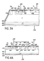
- FIG. 3A represents a schematic sectional view of an integrated structure according to the present invention implementing the circuit of FIG. 1.
- the zones corresponding to the diodes D1, D2 have been indicated at the top of the figure to facilitate understanding. and D3 and to the transistor T1.
- the structure of FIG. 3A comprises an N-type substrate 100 the underside of which is an N-type layer 102 coated with a metallization 104 connected to a terminal 105.
- the N-type layer can be obtained by epitaxy from an N substrate or, on the contrary, it is possible to start from an N type substrate and form the N layer by diffusion.
- the transistor T1 which occupies most of the surface of the wafer comprises a base layer 106 of type P and a layer 108 of emitter of type N.
- the layer 108 of type N is coated with a metallization emitter 110 connected to a terminal 112.
- the base layer 106 is interrupted to allow the formation of a separate P-type zone 114 to form with the layer 100 the diode Dl.
- This separate type P zone it is possible either to form a uniform P layer on the upper surface of the substrate and to isolate a portion of this layer by digging a furrow delimiting zone 114 (see figure 3C), or else proceed by diffusion through a mask to form the layer 106 and the zone 114 separately (see FIG. 3B).
- Diode D2 is formed in layer P of type P in the form of a zone N 115 in a box P 116.
- Diode D3 is also formed in layer 106 of type P in the form of a zone P 118 in a box N 120.
- the area P 114, the area N 115 and the area P 118 are connected by a metallization 122.
- the well N 120 and the base layer 106 of the transistor T1 are connected by a metallization 124.
- the metallization 122 is connected to an input connection 126.
- the well P 116 does not have a fundamental role but has the aim of reducing the gain of the vertical parasitic transistor which would be constituted by the area 115, layer 106 and the collector of the structure.
- this box other methods known in the art could be used to reduce the gain of a parasitic transistor.
- the box P 116 in the vicinity of the junction between the area N 115 and the layer P 106, provision could be made for a diffusion of gold or electronic bombardment to reduce the lifetime of the carriers in this area. and thus reduce the gain of the vertical parasitic transistor.
- the diode Dl particularly rapid and provision may also be made for electronic irradiation or diffusion with gold in this zone. If this solution is chosen which consists in reducing the lifetime of the carriers by electronic irradiation or diffusion of gold, this irradiation or this diffusion will be carried out simultaneously in the zones corresponding to the diodes D1 and D2.
- the hatched zones correspond to layers of silica intended to passivate the junction outcrops and to avoid their short-circuiting by the various metallizations.
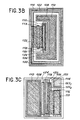
- FIG. 3B represents a top view of an embodiment of an integrated structure corresponding to the schematic section of FIG. 3A.
- the white areas correspond to P-type diffusions; hatched areas with N-type diffusions; the dotted areas to metallizations; and the black dot areas to metallizations on an insulating oxide layer.
- Diffusion 116 completely surrounds the structure. It will be noted that the entire structure could be surrounded by a hatched area if the diffusion 114 (diode Dl) was surrounded on either side by a rise in the layer N of collector 100, that is to say say in the case of a planar type structure.
- the detailed top view of FIG. 3B is only one example of configuration among many possible mask configurations.
- FIG. 3C represents a top view of another embodiment of an integrated structure corresponding to the schematic section of FIG. 3A.
- the structure is of the mesa type and the diffusion 114 is separated from the layer 106 by a groove 150.
- the metallization 122 in the form of two metallizations 122 1 and 122 2 .. To connect these metallizations, one can form on each of them a conductive ball and connect these balls by a bar.
- FIGS. 3B and 3C the same references have been used as in FIG. 3A to designate corresponding elements and layers.
- FIG. 4A illustrates a schematic sectional view of an embodiment of integration according to the present invention of a circuit such as that illustrated in FIG. 2 (excluding the resistors RI and R2).
- a circuit such as that illustrated in FIG. 2 (excluding the resistors RI and R2).
- the various elements already described in relation to Figure 3A and designated by the same references.
- the zones corresponding substantially to the locations of the diodes Dl, D2, D3 and D4 and to the transistors Tl and T2.
- the base layer 106 is also formed an emitter layer of the main transistor T2, this N-type layer being designated by the reference 130.
- the diode D4 is formed by an N 132 area formed in a P-type box 134.
- the N-type layer 108 constituting the emitter of the transistor T1 is connected to the base layer 106 of the transistor T2.
- This connection is represented in the figure by the metallizations 136 and 138 as well as by the conductor 140.
- this assembly 136, 138 and 140 constitutes a single metallization which has been represented in this form only to simplify the representation of the view. sectional.
- the emitter 130 of the transistor T2 is covered with a metallization 142 connected to a connection terminal 144 constituting the emitter output of the Darlington assembly.
- the P type boxes 116 and 134 could be replaced by diffusions of gold or an electronic irradiation carried out in the vicinity of zones 115 and 132 at the same time besides as at vicinity of the zone 114 constituting the diode Dl.
- FIG. 4B represents a top view of an embodiment of an integrated structure corresponding to the schematic section of FIG. 4A.
- the same references designate corresponding layers and zones.
- zone 114 is isolated by a groove 160.
Landscapes
- Bipolar Integrated Circuits (AREA)
- Bipolar Transistors (AREA)
Applications Claiming Priority (2)
| Application Number | Priority Date | Filing Date | Title |
|---|---|---|---|
| FR7913630 | 1979-05-29 | ||
| FR7913630A FR2458146A1 (fr) | 1979-05-29 | 1979-05-29 | Structure integree comportant un transistor et trois diodes antisaturation |
Publications (1)
| Publication Number | Publication Date |
|---|---|
| EP0020233A1 true EP0020233A1 (fr) | 1980-12-10 |
Family
ID=9225965
Family Applications (1)
| Application Number | Title | Priority Date | Filing Date |
|---|---|---|---|
| EP80400695A Withdrawn EP0020233A1 (fr) | 1979-05-29 | 1980-05-20 | Structure intégrée comportant un transistor et trois diodes antisaturation |
Country Status (3)
| Country | Link |
|---|---|
| EP (1) | EP0020233A1 (OSRAM) |
| JP (1) | JPS55158664A (OSRAM) |
| FR (1) | FR2458146A1 (OSRAM) |
Cited By (6)
| Publication number | Priority date | Publication date | Assignee | Title |
|---|---|---|---|---|
| EP0150366A3 (de) * | 1984-01-31 | 1985-09-18 | Siemens Aktiengesellschaft | Schaltungsanordnung zur Minimierung der Wirkung parasitärer Transistorfunktionselemente in integrierten bipolaren Halbleiterschaltkreisen |
| US4665422A (en) * | 1983-08-20 | 1987-05-12 | Mitsubishi Denki Kabushiki Kaisha | Solid state image sensing device |
| FR2598048A1 (fr) * | 1986-04-23 | 1987-10-30 | Fuji Electric Co Ltd | Dispositif semiconducteur a transistors en montage du type dit darlington, a vitesse de commutation accrue |
| GB2240951A (en) * | 1990-02-09 | 1991-08-21 | Canon Kk | Integrated transducer and semiconductor circuit arrays in thermal ink jet printers. |
| EP0630051A1 (en) * | 1993-06-15 | 1994-12-21 | Consorzio per la Ricerca sulla Microelettronica nel Mezzogiorno - CoRiMMe | Integrated structure bipolar switching transistor with controlled storage time |
| EP1191594A3 (de) * | 2000-09-21 | 2004-11-24 | Infineon Technologies AG | Diodenvorrichtung aus zwei monolithisch miteinander integrierten Dioden |
Families Citing this family (3)
| Publication number | Priority date | Publication date | Assignee | Title |
|---|---|---|---|---|
| JPS5658260A (en) * | 1979-10-16 | 1981-05-21 | Matsushita Electronics Corp | Darlington junction type transistor and production thereof |
| JPS58102549A (ja) * | 1981-12-14 | 1983-06-18 | Nippon Telegr & Teleph Corp <Ntt> | 半導体集積回路 |
| JPS6229157A (ja) * | 1985-07-29 | 1987-02-07 | New Japan Radio Co Ltd | 2端子素子 |
Citations (6)
| Publication number | Priority date | Publication date | Assignee | Title |
|---|---|---|---|---|
| FR2101228A1 (OSRAM) * | 1970-08-05 | 1972-03-31 | Ibm | |
| US3913213A (en) * | 1974-08-02 | 1975-10-21 | Trw Inc | Integrated circuit transistor switch |
| FR2282721A1 (fr) * | 1974-08-19 | 1976-03-19 | Rca Corp | Dispositif semi-conducteur |
| US4072981A (en) * | 1975-03-25 | 1978-02-07 | Texas Instruments Incorporated | Fast switching Darlington circuit |
| FR2377706A1 (fr) * | 1977-01-12 | 1978-08-11 | Radiotechnique Compelec | Dispositif semi-conducteur integre du type darlington et son procede de fabrication |
| US4138690A (en) * | 1976-05-11 | 1979-02-06 | Tokyo Shibaura Electric Co., Ltd. | Darlington circuit semiconductor device |
-
1979
- 1979-05-29 FR FR7913630A patent/FR2458146A1/fr active Granted
-
1980
- 1980-05-20 EP EP80400695A patent/EP0020233A1/fr not_active Withdrawn
- 1980-05-28 JP JP7128680A patent/JPS55158664A/ja active Pending
Patent Citations (6)
| Publication number | Priority date | Publication date | Assignee | Title |
|---|---|---|---|---|
| FR2101228A1 (OSRAM) * | 1970-08-05 | 1972-03-31 | Ibm | |
| US3913213A (en) * | 1974-08-02 | 1975-10-21 | Trw Inc | Integrated circuit transistor switch |
| FR2282721A1 (fr) * | 1974-08-19 | 1976-03-19 | Rca Corp | Dispositif semi-conducteur |
| US4072981A (en) * | 1975-03-25 | 1978-02-07 | Texas Instruments Incorporated | Fast switching Darlington circuit |
| US4138690A (en) * | 1976-05-11 | 1979-02-06 | Tokyo Shibaura Electric Co., Ltd. | Darlington circuit semiconductor device |
| FR2377706A1 (fr) * | 1977-01-12 | 1978-08-11 | Radiotechnique Compelec | Dispositif semi-conducteur integre du type darlington et son procede de fabrication |
Cited By (10)
| Publication number | Priority date | Publication date | Assignee | Title |
|---|---|---|---|---|
| US4665422A (en) * | 1983-08-20 | 1987-05-12 | Mitsubishi Denki Kabushiki Kaisha | Solid state image sensing device |
| US4791070A (en) * | 1983-08-20 | 1988-12-13 | Mitsubishi Denki Kabushiki Kaisha | Method of fabricating a solid state image sensing device |
| EP0150366A3 (de) * | 1984-01-31 | 1985-09-18 | Siemens Aktiengesellschaft | Schaltungsanordnung zur Minimierung der Wirkung parasitärer Transistorfunktionselemente in integrierten bipolaren Halbleiterschaltkreisen |
| FR2598048A1 (fr) * | 1986-04-23 | 1987-10-30 | Fuji Electric Co Ltd | Dispositif semiconducteur a transistors en montage du type dit darlington, a vitesse de commutation accrue |
| GB2240951A (en) * | 1990-02-09 | 1991-08-21 | Canon Kk | Integrated transducer and semiconductor circuit arrays in thermal ink jet printers. |
| US5264874A (en) * | 1990-02-09 | 1993-11-23 | Canon Kabushiki Kaisha | Ink jet recording system |
| GB2240951B (en) * | 1990-02-09 | 1994-10-05 | Canon Kk | Ink jet recording system |
| US5567630A (en) * | 1990-02-09 | 1996-10-22 | Canon Kabushiki Kaisha | Method of forming an ink jet recording device, and head using same |
| EP0630051A1 (en) * | 1993-06-15 | 1994-12-21 | Consorzio per la Ricerca sulla Microelettronica nel Mezzogiorno - CoRiMMe | Integrated structure bipolar switching transistor with controlled storage time |
| EP1191594A3 (de) * | 2000-09-21 | 2004-11-24 | Infineon Technologies AG | Diodenvorrichtung aus zwei monolithisch miteinander integrierten Dioden |
Also Published As
| Publication number | Publication date |
|---|---|
| JPS55158664A (en) | 1980-12-10 |
| FR2458146B1 (OSRAM) | 1983-01-21 |
| FR2458146A1 (fr) | 1980-12-26 |
Similar Documents
| Publication | Publication Date | Title |
|---|---|---|
| EP0721218B1 (fr) | Circuit intégré de puissance | |
| EP0409746B1 (fr) | Circuit intégré VDMOS/logique comprenant un transistor vertical déplété et une diode zener | |
| EP0963608B1 (fr) | Circuit de protection d'interface d'abonnes | |
| EP0562982B1 (fr) | Circuit intégré constituant un réseau de diodes de protection | |
| EP0785577A1 (fr) | Composant de protection d'interface de lignes telephoniques | |
| EP0576375A1 (fr) | Structure de diodes de protection de plot | |
| EP0490786B1 (fr) | Circuit de protection programmable et sa réalisation monolithique | |
| EP0490787B1 (fr) | Circuit de protection limitant les surtensions entre limites choisies et son intégration monolithique | |
| EP0020233A1 (fr) | Structure intégrée comportant un transistor et trois diodes antisaturation | |
| EP0620596A1 (fr) | Réseau de diodes monolithique | |
| EP0614232B1 (fr) | Diode de référence dans un circuit intégré bipolaire | |
| EP0543745B1 (fr) | Transistor MOS à zener de protection intégrée | |
| EP1672699B1 (fr) | Commutateur bidirectionnel à commande en tension | |
| EP0022687B1 (fr) | Circuit intégré monolithique équivalent à un transistor associé à trois diodes anti-saturation et son procédé de fabrication | |
| EP3276662B1 (fr) | Structure de protection d'un circuit intégré contre les décharges électrostatiques | |
| EP0872891A1 (fr) | Composant de protection d'interface de lignes téléphoniques | |
| EP0521802B1 (fr) | Diode à avalanche dans un circuit intégré bipolaire | |
| EP0599739B1 (fr) | Thyristor et assemblage de thyristors à cathode commune | |
| FR2797525A1 (fr) | Commutateur bidirectionnel a performances en commutation ameliorees | |
| EP0742592B1 (fr) | Composant de protection sensible de circuit d'interface de lignes d'abonnés | |
| EP1544919B1 (fr) | Triac | |
| EP0704903B1 (fr) | Composant semiconducteur d'alimentation, de recirculation et de démagnétisation d'une charge selfique | |
| FR2488046A1 (fr) | Dispositif de puissance a commande par transistor dmos | |
| FR2982077A1 (fr) | Triac a amplification de gachette | |
| EP0098209B1 (fr) | Transistor de commutation de puissance à structure digitée |
Legal Events
| Date | Code | Title | Description |
|---|---|---|---|
| PUAI | Public reference made under article 153(3) epc to a published international application that has entered the european phase |
Free format text: ORIGINAL CODE: 0009012 |
|
| AK | Designated contracting states |
Designated state(s): DE GB IT NL |
|
| 17P | Request for examination filed |
Effective date: 19810306 |
|
| STAA | Information on the status of an ep patent application or granted ep patent |
Free format text: STATUS: THE APPLICATION IS DEEMED TO BE WITHDRAWN |
|
| 18D | Application deemed to be withdrawn |
Effective date: 19830121 |
|
| RIN1 | Information on inventor provided before grant (corrected) |
Inventor name: QUOIRIN, JEAN-BAPTISTE |