EP0020233A1 - Structure intégrée comportant un transistor et trois diodes antisaturation - Google Patents
Structure intégrée comportant un transistor et trois diodes antisaturation Download PDFInfo
- Publication number
- EP0020233A1 EP0020233A1 EP80400695A EP80400695A EP0020233A1 EP 0020233 A1 EP0020233 A1 EP 0020233A1 EP 80400695 A EP80400695 A EP 80400695A EP 80400695 A EP80400695 A EP 80400695A EP 0020233 A1 EP0020233 A1 EP 0020233A1
- Authority
- EP
- European Patent Office
- Prior art keywords
- layer
- type
- conductivity
- box
- zone
- Prior art date
- Legal status (The legal status is an assumption and is not a legal conclusion. Google has not performed a legal analysis and makes no representation as to the accuracy of the status listed.)
- Withdrawn
Links
- 238000001465 metallisation Methods 0.000 claims description 24
- 238000009792 diffusion process Methods 0.000 claims description 20
- 239000000758 substrate Substances 0.000 claims description 14
- PCHJSUWPFVWCPO-UHFFFAOYSA-N gold Chemical compound [Au] PCHJSUWPFVWCPO-UHFFFAOYSA-N 0.000 claims description 6
- 239000010931 gold Substances 0.000 claims description 6
- 229910052737 gold Inorganic materials 0.000 claims description 6
- 238000000034 method Methods 0.000 claims description 5
- 238000004519 manufacturing process Methods 0.000 claims description 4
- 239000000969 carrier Substances 0.000 claims description 3
- 230000015572 biosynthetic process Effects 0.000 description 11
- 230000010354 integration Effects 0.000 description 3
- 230000003071 parasitic effect Effects 0.000 description 3
- VYPSYNLAJGMNEJ-UHFFFAOYSA-N Silicium dioxide Chemical compound O=[Si]=O VYPSYNLAJGMNEJ-UHFFFAOYSA-N 0.000 description 2
- 241001415961 Gaviidae Species 0.000 description 1
- 239000004020 conductor Substances 0.000 description 1
- 238000000407 epitaxy Methods 0.000 description 1
- 239000004065 semiconductor Substances 0.000 description 1
- 239000000377 silicon dioxide Substances 0.000 description 1
Images

Classifications
-
- H—ELECTRICITY
- H01—ELECTRIC ELEMENTS
- H01L—SEMICONDUCTOR DEVICES NOT COVERED BY CLASS H10
- H01L27/00—Devices consisting of a plurality of semiconductor or other solid-state components formed in or on a common substrate
- H01L27/02—Devices consisting of a plurality of semiconductor or other solid-state components formed in or on a common substrate including semiconductor components specially adapted for rectifying, oscillating, amplifying or switching and having potential barriers; including integrated passive circuit elements having potential barriers
- H01L27/04—Devices consisting of a plurality of semiconductor or other solid-state components formed in or on a common substrate including semiconductor components specially adapted for rectifying, oscillating, amplifying or switching and having potential barriers; including integrated passive circuit elements having potential barriers the substrate being a semiconductor body
- H01L27/08—Devices consisting of a plurality of semiconductor or other solid-state components formed in or on a common substrate including semiconductor components specially adapted for rectifying, oscillating, amplifying or switching and having potential barriers; including integrated passive circuit elements having potential barriers the substrate being a semiconductor body including only semiconductor components of a single kind
- H01L27/082—Devices consisting of a plurality of semiconductor or other solid-state components formed in or on a common substrate including semiconductor components specially adapted for rectifying, oscillating, amplifying or switching and having potential barriers; including integrated passive circuit elements having potential barriers the substrate being a semiconductor body including only semiconductor components of a single kind including bipolar components only
- H01L27/0823—Devices consisting of a plurality of semiconductor or other solid-state components formed in or on a common substrate including semiconductor components specially adapted for rectifying, oscillating, amplifying or switching and having potential barriers; including integrated passive circuit elements having potential barriers the substrate being a semiconductor body including only semiconductor components of a single kind including bipolar components only including vertical bipolar transistors only
- H01L27/0825—Combination of vertical direct transistors of the same conductivity type having different characteristics,(e.g. Darlington transistors)
-
- H—ELECTRICITY
- H01—ELECTRIC ELEMENTS
- H01L—SEMICONDUCTOR DEVICES NOT COVERED BY CLASS H10
- H01L27/00—Devices consisting of a plurality of semiconductor or other solid-state components formed in or on a common substrate
- H01L27/02—Devices consisting of a plurality of semiconductor or other solid-state components formed in or on a common substrate including semiconductor components specially adapted for rectifying, oscillating, amplifying or switching and having potential barriers; including integrated passive circuit elements having potential barriers
- H01L27/0203—Particular design considerations for integrated circuits
- H01L27/0248—Particular design considerations for integrated circuits for electrical or thermal protection, e.g. electrostatic discharge [ESD] protection
-
- H—ELECTRICITY
- H01—ELECTRIC ELEMENTS
- H01L—SEMICONDUCTOR DEVICES NOT COVERED BY CLASS H10
- H01L27/00—Devices consisting of a plurality of semiconductor or other solid-state components formed in or on a common substrate
- H01L27/02—Devices consisting of a plurality of semiconductor or other solid-state components formed in or on a common substrate including semiconductor components specially adapted for rectifying, oscillating, amplifying or switching and having potential barriers; including integrated passive circuit elements having potential barriers
- H01L27/04—Devices consisting of a plurality of semiconductor or other solid-state components formed in or on a common substrate including semiconductor components specially adapted for rectifying, oscillating, amplifying or switching and having potential barriers; including integrated passive circuit elements having potential barriers the substrate being a semiconductor body
- H01L27/06—Devices consisting of a plurality of semiconductor or other solid-state components formed in or on a common substrate including semiconductor components specially adapted for rectifying, oscillating, amplifying or switching and having potential barriers; including integrated passive circuit elements having potential barriers the substrate being a semiconductor body including a plurality of individual components in a non-repetitive configuration
- H01L27/07—Devices consisting of a plurality of semiconductor or other solid-state components formed in or on a common substrate including semiconductor components specially adapted for rectifying, oscillating, amplifying or switching and having potential barriers; including integrated passive circuit elements having potential barriers the substrate being a semiconductor body including a plurality of individual components in a non-repetitive configuration the components having an active region in common
- H01L27/0744—Devices consisting of a plurality of semiconductor or other solid-state components formed in or on a common substrate including semiconductor components specially adapted for rectifying, oscillating, amplifying or switching and having potential barriers; including integrated passive circuit elements having potential barriers the substrate being a semiconductor body including a plurality of individual components in a non-repetitive configuration the components having an active region in common without components of the field effect type
- H01L27/075—Bipolar transistors in combination with diodes, or capacitors, or resistors, e.g. lateral bipolar transistor, and vertical bipolar transistor and resistor
- H01L27/0755—Vertical bipolar transistor in combination with diodes, or capacitors, or resistors
- H01L27/0761—Vertical bipolar transistor in combination with diodes only
Definitions
- the present invention relates to an integrated structure comprising a transistor assembly, the input transistor being provided with anti-saturation diodes, as well as the method of manufacturing such a structure.
- anti-saturation diodes connected from the as shown in Figure 1.
- the input to the base of the NPN transistor Tl is via two anti-parallel diodes D2 and D3. This input is connected to the collector of the transistor Tl via a diode Dl oriented as shown in the figure.
- a diode D4 commonly called a destocking diode, is often included in a Darlington circuit between the emitter and the base of the transistor Tl (or rather, in the particular case shown, input 10) to reduce the time of circuit storage.
- An output diode D5 may be present between the emitter and the collector of transistor T2.
- circuits including the transistors T1, T2 and the diode D4 in integrated form.
- the object of the present invention is to provide a monolithic integrated circuit including the transistor Tl and all of its anti-saturation diodes Dl, D2, D3, this integration being compatible with the integration of a Darlington assembly as in the case of FIG. 2.
- each of the diodes D1, D2, D3 and D4 can in fact consist of several diodes in series.
- the present invention provides an integrated structure comprising a substrate of a first type of conductivity, the underside of which serves as a collector; a first base layer of a second type of conductivity covering most of the upper face of the substrate; a second emitter layer of the first type of conductivity covering most of the first layer, the underside of the substrate being covered with a collector metallization and the second emitter layer being covered with an emitter metallization; a first zone of the second type of conductivity, formed in the upper face of the substrate and separated from the first layer; a second zone of the first type of conductivity formed in a first box of the second type of conductivity with a high doping level formed in the first layer; a third zone of the second type of conductivity formed in a second box of the first type of conductivity formed in the first layer; a first metallization connecting the visible upper faces of the first, second and third zones; and a second metallization connecting the visible upper faces of the second box and the first layer.
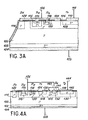
- FIG. 3A represents a schematic sectional view of an integrated structure according to the present invention implementing the circuit of FIG. 1.
- the zones corresponding to the diodes D1, D2 have been indicated at the top of the figure to facilitate understanding. and D3 and to the transistor T1.
- the structure of FIG. 3A comprises an N-type substrate 100 the underside of which is an N-type layer 102 coated with a metallization 104 connected to a terminal 105.
- the N-type layer can be obtained by epitaxy from an N substrate or, on the contrary, it is possible to start from an N type substrate and form the N layer by diffusion.
- the transistor T1 which occupies most of the surface of the wafer comprises a base layer 106 of type P and a layer 108 of emitter of type N.
- the layer 108 of type N is coated with a metallization emitter 110 connected to a terminal 112.
- the base layer 106 is interrupted to allow the formation of a separate P-type zone 114 to form with the layer 100 the diode Dl.
- This separate type P zone it is possible either to form a uniform P layer on the upper surface of the substrate and to isolate a portion of this layer by digging a furrow delimiting zone 114 (see figure 3C), or else proceed by diffusion through a mask to form the layer 106 and the zone 114 separately (see FIG. 3B).
- Diode D2 is formed in layer P of type P in the form of a zone N 115 in a box P 116.
- Diode D3 is also formed in layer 106 of type P in the form of a zone P 118 in a box N 120.
- the area P 114, the area N 115 and the area P 118 are connected by a metallization 122.
- the well N 120 and the base layer 106 of the transistor T1 are connected by a metallization 124.
- the metallization 122 is connected to an input connection 126.
- the well P 116 does not have a fundamental role but has the aim of reducing the gain of the vertical parasitic transistor which would be constituted by the area 115, layer 106 and the collector of the structure.
- this box other methods known in the art could be used to reduce the gain of a parasitic transistor.
- the box P 116 in the vicinity of the junction between the area N 115 and the layer P 106, provision could be made for a diffusion of gold or electronic bombardment to reduce the lifetime of the carriers in this area. and thus reduce the gain of the vertical parasitic transistor.
- the diode Dl particularly rapid and provision may also be made for electronic irradiation or diffusion with gold in this zone. If this solution is chosen which consists in reducing the lifetime of the carriers by electronic irradiation or diffusion of gold, this irradiation or this diffusion will be carried out simultaneously in the zones corresponding to the diodes D1 and D2.
- the hatched zones correspond to layers of silica intended to passivate the junction outcrops and to avoid their short-circuiting by the various metallizations.
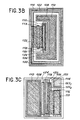
- FIG. 3B represents a top view of an embodiment of an integrated structure corresponding to the schematic section of FIG. 3A.
- the white areas correspond to P-type diffusions; hatched areas with N-type diffusions; the dotted areas to metallizations; and the black dot areas to metallizations on an insulating oxide layer.
- Diffusion 116 completely surrounds the structure. It will be noted that the entire structure could be surrounded by a hatched area if the diffusion 114 (diode Dl) was surrounded on either side by a rise in the layer N of collector 100, that is to say say in the case of a planar type structure.
- the detailed top view of FIG. 3B is only one example of configuration among many possible mask configurations.
- FIG. 3C represents a top view of another embodiment of an integrated structure corresponding to the schematic section of FIG. 3A.
- the structure is of the mesa type and the diffusion 114 is separated from the layer 106 by a groove 150.
- the metallization 122 in the form of two metallizations 122 1 and 122 2 .. To connect these metallizations, one can form on each of them a conductive ball and connect these balls by a bar.
- FIGS. 3B and 3C the same references have been used as in FIG. 3A to designate corresponding elements and layers.
- FIG. 4A illustrates a schematic sectional view of an embodiment of integration according to the present invention of a circuit such as that illustrated in FIG. 2 (excluding the resistors RI and R2).
- a circuit such as that illustrated in FIG. 2 (excluding the resistors RI and R2).
- the various elements already described in relation to Figure 3A and designated by the same references.
- the zones corresponding substantially to the locations of the diodes Dl, D2, D3 and D4 and to the transistors Tl and T2.
- the base layer 106 is also formed an emitter layer of the main transistor T2, this N-type layer being designated by the reference 130.
- the diode D4 is formed by an N 132 area formed in a P-type box 134.
- the N-type layer 108 constituting the emitter of the transistor T1 is connected to the base layer 106 of the transistor T2.
- This connection is represented in the figure by the metallizations 136 and 138 as well as by the conductor 140.
- this assembly 136, 138 and 140 constitutes a single metallization which has been represented in this form only to simplify the representation of the view. sectional.
- the emitter 130 of the transistor T2 is covered with a metallization 142 connected to a connection terminal 144 constituting the emitter output of the Darlington assembly.
- the P type boxes 116 and 134 could be replaced by diffusions of gold or an electronic irradiation carried out in the vicinity of zones 115 and 132 at the same time besides as at vicinity of the zone 114 constituting the diode Dl.
- FIG. 4B represents a top view of an embodiment of an integrated structure corresponding to the schematic section of FIG. 4A.
- the same references designate corresponding layers and zones.
- zone 114 is isolated by a groove 160.
Landscapes
- Engineering & Computer Science (AREA)
- Power Engineering (AREA)
- Physics & Mathematics (AREA)
- Condensed Matter Physics & Semiconductors (AREA)
- General Physics & Mathematics (AREA)
- Computer Hardware Design (AREA)
- Microelectronics & Electronic Packaging (AREA)
- Bipolar Transistors (AREA)
- Bipolar Integrated Circuits (AREA)
Abstract
La présente invention concerne une structure intégrée comportant un transistor et trois diodes anti-saturation. La structure selon la présente invention comprend un transistor principal (T1) formé des couches (108, 106 et 100), une première diode (D1) constituée des couches (114 et 100), une deuxième diode (D2) constituée des couches (115, 116 et 106), et une troisième diode (D3) constituée des couches (118, 120 et 106). Application aux transistors de commutation.
Description
- La présente invention concerne une structure intégrée comprenant un montage à transistor, le transistor d'entrée étant muni de diodes anti-saturation, ainsi que le procédé de fabrication d'une telle structure.
- Il est connu dans la technique que pour améliorer certaines caractéristiques d'un transistor, notamment pour des transistors de puissance fonctionnant en commutation, il peut être souhaitable d'associer à ce transistor trois diodes, dites diodes d'anti-saturation, connectées de la façon représentée en figure 1. L'entrée vers la base du transistor NPN Tl se fait par l'intermédiaire de deux diodes en anti-parallèle D2 et D3. Cette entrée est connectée au collecteur du transistor Tl par l'intermédiaire d'une diode Dl orientée de la façon représentée dans la figure.
- Cette prévision de diodes anti-saturation s'applique également, comme cela est connu dans la technique , au cas d'un montage Darlington comme cela est représenté dans la figure 2. On peut voir dans cette figure, outre les éléments déjà décrits en relation avec la figure 1, un transistor T2 dont la base est reliée à l'émetteur du transistor Tl et le collecteur au collecteur du transistor Tl, cette connexion commune de collecteur servant de sortie collecteur du montage et l'émetteur du transistor T2 servant de sortie d'émetteur du montage Darlington. De façon générale, il est également prévu une résistance RI entre les émetteurs des transistors Tl et T2 et une résistance R2 entre l'émetteur du transistor Tl et l'entrée 10 du circuit. En outre, une diode D4, couramment appelée diode de déstockage, est souvent incluse dans un montage Darlington entre l'émetteur et la base du transistor Tl (ou plutôt, dans le cas particulier représenté, l'entrée 10) pour diminuer le temps de stockage du circuit. Une diode de sortie D5 peut être présente entre l'émetteur et le collecteur du transistor T2.
- On connaît dans la technique, des circuits incluant les transistors Tl, T2 et la diode D4 sous forme intégrée.
- La présente invention a pour objet de prévoir un circuit intégré monolithique incluant le transistor Tl et l'ensemble de ses diodes d'anti-saturation Dl, D2, D3, cette intégration étant compatible avec l'intégration d'un ensemble Darlington comme dans le cas de la figure 2. Dans la pratique, chacune des diodes Dl, D2, D3 et D4 peut en fait être constituée de plusieurs diodes en série.
- Pour atteindre cet objet, la présente invention prévoit une structure intégrée comprenant un substrat d'un premier type de conductivité dont la face inférieure sert de collecteur ; une première couche de base d'un deuxième type de conductivité recouvrant la plus grande partie de la face supérieure du substrat ; une deuxième couche d'émetteur du premier type de conductivité recouvrant la plus grande partie de la première couche, la face inférieure du substrat étant recouverte d'une métallisation de collecteur et la deuxième couche d'émetteur étant recouverte d'une métallisation d'émetteur ; une première zone du deuxième type de conductivité, formée dans la face supérieure du substrat et séparée de la première couche ; une deuxième zone du premier type de conductivité formée dans un premier caisson du deuxième type de conductivité à niveau de dopage élevé ménagé dans la première couche ; une troisième zone du deuxième type de conductivité formée dans un deuxième caisson du premier type de conductivité ménagé dans la première couche ; une première métallisation reliant les faces supérieures apparentes des première , deuxième et troisième zones ; et une deuxième métallisation reliant les faces supérieures apparentes du deuxième caisson et de la première couche. Selon un aspect de l'invention, chacun des premier et deuxième caissons peut contenir plusieurs diodes en série emboîtées.
- Ces objets, caractéristiques et avantages ainsi que d'autres de la présente invention seront exposés plus en détail dans la description suivante de modes de réalisation particuliers faite en relation avec les figures jointes parmi lesquelles :
- - les figures 1 et 2 représentent sous forme symbolique les circuits que vise à réaliser la structure intégrée selon la présente invention ;
- - la figure 3A représente une vue en coupe schématique d'un mode de réalisation de structure intégrée associant un transistor et ses diodes anti-saturation selon la présente invention ;
- - les figures 3B et 3C représentent diverses vues de dessus correspondant à des variantes du mode de réalisation de la figure 3A ;
- - la figure 4A représente une vue en coupe schématique d'un montage Darlington muni d'une diode de déstockage et de diodes anti-saturation intégrées selon un mode de réalisation de la présente invention ; et
- - la figure 4B représente une vue de dessus correspondant au mode de réalisation de la figure 4A.
- On notera que dans les diverses figures, comme cela est classique dans les représentations schématiques de dispositifs à semiconducteur, ni les épaisseurs, ni les dimensions relatives des diverses couches et surfaces ne sont tracées à l'échelle. Pour une réalisation pratique, l'homme de l'art se réfèrera aux connaissances technologiques usuelles dans le domaine considéré.
- La figure 3A représente une vue en coupe schématique d'une structure intégrée selon la présente invention mettant en oeuvre le circuit de la figure 1. On a indiqué en haut de la figure pour faciliter la compréhension, les zones correspondant sensiblement aux diodes Dl, D2 et D3 et au transistor Tl. La structure de la figure 3A comprend un substrat 100 de type N dont la face inférieure est une couche 102 de type N revêtue d'une métallisation 104 reliée à une borne 105. La couche de type N peut être obtenue par épitaxie à partir d'un substrat N ou , au contraire, on peut partir d'un substrat de type N et former la couche N par diffusion. Le transistor Tl qui occupe la plus grande partie de la surface de la plaquette comprend une couche de base 106 du type P et une couche 108 d'émetteur de type N. La couche 108 de type N est revêtue d'une métallisation d'émetteur 110 reliée à une borne 112. La couche de base 106 est interrompue pour permettre la formation d'une zone de type P séparée 114 pour former avec la couche 100 la diode Dl. Pour obtenir cette zone de type P séparée, on peut , ou bien procéder à la formation d'une couche P uniforme à la surface supérieure du substrat et isoler une portion de cette couche par creusage d'un sillon délimitant la zone 114 (voir figure 3C), ou bien procéder par diffusion à travers un masque pour former séparément la couche 106 et la zone 114 (voir figure 3B).
- La diode D2 est formée dans la chouche 106 de type P sous forme d'une zone N 115 dans un caisson P 116. La diode D3 est également formée dans la couche 106 de type P sous forme d'une zone P 118 dans un caisson N 120. La zone P 114, la zone N 115 et la zone P 118 sont connectées par une métallisation 122. Le caisson N 120 et la couche de base 106 du transistor Tl sont connectés par une métallisation 124. La métallisation 122 est reliée à une connexion d'entrée 126.
- Alors que la fabrication du transistor Tl seul ne mettrait en jeu que deux étapes de diffusion-masquage sur la surface supérieure du substrat 100 (une diffusion pour la formation de la couche 106 de type P et une diffusion pour la formation de la couche 108 de type N), la réalisation de la structure intégrée selon la présente invention met en jeu deux étapes de diffusion-masquage supplémentaires pour la diffusion des diodes D2 et D3 et plus particulièrement du caisson P 116 et de la couche P 118. La séquence des étapes de diffusion-masquage est la suivante :
- - formation de la couche P 106 et de la zone P 114
- - formation du caisson P 116
- - formation de la couche N 108, de la zone N 115 et du caisson N+ 120
- - formation de la zone P 118.
- On notera que, si le caisson N 120 est nécessaire pour obtenir une diode D3 selon la bonne polarité, le caisson P 116 n'a pas un rôle fondamental mais a pour but de réduire le gain du transistor parasite vertical qui serait constitué par la zone 115, la couche 106 et le collecteur de la structure. Au lieu de ce caisson, on pourrait utiliser d'autres procédés connus dans la technique pour diminuer le gain d'un transistor parasite. Par exemple, il pourrait être prévu au lieu du caisson P 116, au voisinage de la jonction entre la zone N 115 et la couche P 106, une diffusion d'or ou un bombardement électronique pour réduire la durée de vie des porteurs dans cette zone et réduire ainsi le gain du transistor parasite vertical. De même, il est souhaitable de rendre la diode Dl particulièrement rapide et on pourra également prévoir une irradiation électronique ou une diffusion à l'or dans cette zone. Si l'on choisit cette solution qui consiste à réduire la durée de vie des porteurs par irradiation électronique ou diffusion d'or, cette irradiation ou cette diffusion seront effectuées simultanément dans les zones correspondant aux diodes Dl et D2.
- Dans la figure 3A, les zones hachurées correspondent à des couches de silice destinées à passiver les affleurements de jonction et à éviter leur mise en court-circuit par les diverses métallisations.
- La figure 3B représente une vue de dessus d'un mode de réalisation d'une structure intégrée correspondant à la coupe schématique de la figure 3A. Les zones blanches correspondent à des diffusions de type P ; les zones hachurées à des diffusions de type N ; les zones en pointillés à des métallisations ; et les zones à points noirs à des métallisations sur couche d'oxyde isolante. La diffusion 116 entoure complètement la structure. On notera que l'ensemble de la structure pourrait être entouré d'une zone hachurée si la diffusion 114 (diode Dl) était entourée de part et d'autre par une remontée de la couche N de collecteur 100, c'est-à-dire dans le cas d'une structure de type planar. Bien entendu la vue de dessus détaillée de la figure 3B ne constitue qu'un exemple de configuration parmi de nombreuses configurations de masques possibles.
- La figure 3C représente une vue de dessus d'un autre mode de réalisation d'une structure intégrée correspondant à la coupe schématique de la figure 3A. Dans l'exemple représenté, la structure est de type mesa et la diffusion 114 est séparée de la couche 106 par un sillon 150. Dans certains cas, il est difficile de déposer une métallisation 122 recouvrant le sillon 150. On a donc représenté dans la figure, la métallisation 122 sous forme de deux métallisations 1221 et 1222.. Pour connecter ces métallisations, on pourra former sur chacune d'elles une bille conductrice et relier ces billes par une barrette.
- Dans les figures 3B et 3C, on a utilisé les mêmes références que dans la figure 3A pour désigner des éléments et couches correspondants.
- La figure 4A illustre une vue en coupe schématique d'un mode de réalisation d'intégration selon la présente invention d'un circuit tel que celui illustré en figure 2 (à l'exclusion des résistances RI et R2). On retrouve dans la partie gauche de cette figure les divers éléments déjà décrits en relation avec la figure 3A et désignés par les mêmes références. 0n a à nouveau indiqué à la partie supérieure de la figure les zones correspondant sensiblement aux emplacements des diodes Dl, D2, D3 et D4 et aux transistors Tl et T2. Dans la couche de base 106 est en outre formée une couche d'émetteur du transistor principal T2, cette couche de type N étant désignée par la référence 130. La diode D4 est formée d'une zone N 132 ménagée dans un caisson de type P 134. La couche de type N 108 constituant l'émetteur du transistor Tl est reliée à la couche de base 106 du transistor T2. Cette connexion est représentée dans la figure par les métallisations 136 et 138 ainsi que par le conducteur 140. Dans la pratique, cet ensemble 136, 138 et 140 constitue une métallisation unique qui a été représentée sous cette forme uniquement pour simplifier la représentation de la vue en coupe. L'émetteur 130 du transistor T2 est recouvert d'une métallisation 142 reliée à une borne de connexion 144 constituant la sortie d'émetteur du montage Darlington. A nouveau, comme dans le cas de la figure 3A, les caissons de type P 116 et 134 pourraient être remplacés par des diffusions d'or ou une irradiation électronique effectuées au voisinage des zones 115 et 132 en même temps d'ailleurs qu'au voisinage de la zone 114 constituant la diode Dl.
- La figure 4B représente une vue de dessus d'un mode de réalisation d'une structure intégrée correspondant à la coupe schématique de la figure 4A. De mêmes références désignent des couches et zones correspondantes. Ici la zone 114 est isolée par un sillon 160.
- Bien entendu la présente invention est susceptible de nombreuses variantes. Par exemple, l'irradiation électronique peut être remplacée par une irradiation aux rayons X ou gamma.
Claims (8)
1 - Structure intégrée monolithique comportant un transistor et ses trois diodes anti-saturation, comprenant un substrat (100) d'un premier type de conductivité dont la face inférieure constitue le collecteur du transistor ; une première couche de base (106) d'un deuxième type de conductivité recouvrant la plus grande partie de la face supérieure du substrat ; et une deuxième couche d'émetteur (108) du premier type de conductivité recouvrant la plus grande partie de la première couche ; la face inférieure du substrat étant recouverte d'une métallisation de collecteur (104) et la deuxième couche d'émetteur étant recouverte d'une métallisation d'émetteur (110) ; caractérisée en ce qu'elle comprend :
- une première zone (114) du deuxième type de conductivité formée dans la face supérieure du substrat et séparée de la première couche ;
- une deuxième zone (115) du premier type de conductivité formée dans un premier caisson (116) ménagé dans la première couche (106) ;
- une troisième zone (118) du deuxième type de conductivité formée dans un deuxième caisson (120) du premier type de conductivité ménagé dans la première couche ;
- une première métallisation (122) reliant les faces supérieures apparentes des première (114), deuxième (115) et troisième (118) zones ; et
- une deuxième métallisation (124) reliant les faces supérieures apparentes du deuxième caisson (120) et de la première couche (106).
2 - Structure selon la revendication 1, caractérisée en ce que le premier caisson (116) est constitué d'une zone du deuxième type de conductivité.
3 - Structure selon la revendication 1, caractérisée en ce que le premier caisson est constitué d'une partie de la première couche dans laquelle la durée de vie des porteurs a été réduite par un processus du type diffusion d'or ou irradiation .
4 - Structure selon la revendication l, caractérisée en ce qu'elle comprend en outre des couches, zones et métallisations propres à former un second transistor connecté au premier selon un montage Darlington.
5 - Procédé de fabrication de structure selon la revendication 1, à partir d'un substrat d'un premier type de conductivité, caractérisé en ce qu'il comprend les étapes suivantes :
a) former simultanément la première couche (106) et la première zone (114) ;
b) former le premier caisson (116) ;
c) former simultanément la deuxième zone (115), le deuxième caisson (120) et la deuxième couche (108) ; et
d) former la troisième zone (118).
6 - Procédé selon la revendication 5, caractérisé en ce que les diverses étapes sont des étapes de masquage-diffusion et en ce que le premier caisson est constitué d'une couche du deuxième type de conductivité.
7 - Procédé selon la revendication 5, caractérisé en ce que les étapes a) , c) et d) sont des étapes de masquage-diffusion et en ce que l'étape b) est une étape de diffusion d'or réalisée simultanément au voisinage des première et deuxième zones.
8 - Procédé selon la revendication 5, caractérisé en ce que l'étape a) , c) et d) sont des étapes de diffusion et en ce que l'étape b) est une étape d'irradiation électronique réalisée au voisinage de la première zone simultanément avec une irradiation au voisinage de la deuxième zone.
Applications Claiming Priority (2)
| Application Number | Priority Date | Filing Date | Title |
|---|---|---|---|
| FR7913630 | 1979-05-29 | ||
| FR7913630A FR2458146A1 (fr) | 1979-05-29 | 1979-05-29 | Structure integree comportant un transistor et trois diodes antisaturation |
Publications (1)
| Publication Number | Publication Date |
|---|---|
| EP0020233A1 true EP0020233A1 (fr) | 1980-12-10 |
Family
ID=9225965
Family Applications (1)
| Application Number | Title | Priority Date | Filing Date |
|---|---|---|---|
| EP80400695A Withdrawn EP0020233A1 (fr) | 1979-05-29 | 1980-05-20 | Structure intégrée comportant un transistor et trois diodes antisaturation |
Country Status (3)
| Country | Link |
|---|---|
| EP (1) | EP0020233A1 (fr) |
| JP (1) | JPS55158664A (fr) |
| FR (1) | FR2458146A1 (fr) |
Cited By (6)
| Publication number | Priority date | Publication date | Assignee | Title |
|---|---|---|---|---|
| EP0150366A2 (fr) * | 1984-01-31 | 1985-08-07 | Siemens Aktiengesellschaft | Circuit pour minimiser l'effet d'éléments de fonction transistor-parasitaires dans les circuits semi-conducteurs bipolaires intégrés |
| US4665422A (en) * | 1983-08-20 | 1987-05-12 | Mitsubishi Denki Kabushiki Kaisha | Solid state image sensing device |
| FR2598048A1 (fr) * | 1986-04-23 | 1987-10-30 | Fuji Electric Co Ltd | Dispositif semiconducteur a transistors en montage du type dit darlington, a vitesse de commutation accrue |
| GB2240951A (en) * | 1990-02-09 | 1991-08-21 | Canon Kk | Integrated transducer and semiconductor circuit arrays in thermal ink jet printers. |
| EP0630051A1 (fr) * | 1993-06-15 | 1994-12-21 | Consorzio per la Ricerca sulla Microelettronica nel Mezzogiorno - CoRiMMe | Structure intégrée d'un transistor bipolaire ou commutation ayant un temps d'emmagasinage contrôlé |
| EP1191594A2 (fr) * | 2000-09-21 | 2002-03-27 | Infineon Technologies AG | Dispositif de diode comprenant deux diodes monolithiquement intégrés |
Families Citing this family (3)
| Publication number | Priority date | Publication date | Assignee | Title |
|---|---|---|---|---|
| JPS5658260A (en) * | 1979-10-16 | 1981-05-21 | Matsushita Electronics Corp | Darlington junction type transistor and production thereof |
| JPS58102549A (ja) * | 1981-12-14 | 1983-06-18 | Nippon Telegr & Teleph Corp <Ntt> | 半導体集積回路 |
| JPS6229157A (ja) * | 1985-07-29 | 1987-02-07 | New Japan Radio Co Ltd | 2端子素子 |
Citations (6)
| Publication number | Priority date | Publication date | Assignee | Title |
|---|---|---|---|---|
| FR2101228A1 (fr) * | 1970-08-05 | 1972-03-31 | Ibm | |
| US3913213A (en) * | 1974-08-02 | 1975-10-21 | Trw Inc | Integrated circuit transistor switch |
| FR2282721A1 (fr) * | 1974-08-19 | 1976-03-19 | Rca Corp | Dispositif semi-conducteur |
| US4072981A (en) * | 1975-03-25 | 1978-02-07 | Texas Instruments Incorporated | Fast switching Darlington circuit |
| FR2377706A1 (fr) * | 1977-01-12 | 1978-08-11 | Radiotechnique Compelec | Dispositif semi-conducteur integre du type darlington et son procede de fabrication |
| US4138690A (en) * | 1976-05-11 | 1979-02-06 | Tokyo Shibaura Electric Co., Ltd. | Darlington circuit semiconductor device |
-
1979
- 1979-05-29 FR FR7913630A patent/FR2458146A1/fr active Granted
-
1980
- 1980-05-20 EP EP80400695A patent/EP0020233A1/fr not_active Withdrawn
- 1980-05-28 JP JP7128680A patent/JPS55158664A/ja active Pending
Patent Citations (6)
| Publication number | Priority date | Publication date | Assignee | Title |
|---|---|---|---|---|
| FR2101228A1 (fr) * | 1970-08-05 | 1972-03-31 | Ibm | |
| US3913213A (en) * | 1974-08-02 | 1975-10-21 | Trw Inc | Integrated circuit transistor switch |
| FR2282721A1 (fr) * | 1974-08-19 | 1976-03-19 | Rca Corp | Dispositif semi-conducteur |
| US4072981A (en) * | 1975-03-25 | 1978-02-07 | Texas Instruments Incorporated | Fast switching Darlington circuit |
| US4138690A (en) * | 1976-05-11 | 1979-02-06 | Tokyo Shibaura Electric Co., Ltd. | Darlington circuit semiconductor device |
| FR2377706A1 (fr) * | 1977-01-12 | 1978-08-11 | Radiotechnique Compelec | Dispositif semi-conducteur integre du type darlington et son procede de fabrication |
Cited By (12)
| Publication number | Priority date | Publication date | Assignee | Title |
|---|---|---|---|---|
| US4665422A (en) * | 1983-08-20 | 1987-05-12 | Mitsubishi Denki Kabushiki Kaisha | Solid state image sensing device |
| US4791070A (en) * | 1983-08-20 | 1988-12-13 | Mitsubishi Denki Kabushiki Kaisha | Method of fabricating a solid state image sensing device |
| EP0150366A2 (fr) * | 1984-01-31 | 1985-08-07 | Siemens Aktiengesellschaft | Circuit pour minimiser l'effet d'éléments de fonction transistor-parasitaires dans les circuits semi-conducteurs bipolaires intégrés |
| EP0150366A3 (fr) * | 1984-01-31 | 1985-09-18 | Siemens Aktiengesellschaft | Circuit pour minimiser l'effet d'éléments de fonction transistor-parasitaires dans les circuits semi-conducteurs bipolaires intégrés |
| FR2598048A1 (fr) * | 1986-04-23 | 1987-10-30 | Fuji Electric Co Ltd | Dispositif semiconducteur a transistors en montage du type dit darlington, a vitesse de commutation accrue |
| GB2240951A (en) * | 1990-02-09 | 1991-08-21 | Canon Kk | Integrated transducer and semiconductor circuit arrays in thermal ink jet printers. |
| US5264874A (en) * | 1990-02-09 | 1993-11-23 | Canon Kabushiki Kaisha | Ink jet recording system |
| GB2240951B (en) * | 1990-02-09 | 1994-10-05 | Canon Kk | Ink jet recording system |
| US5567630A (en) * | 1990-02-09 | 1996-10-22 | Canon Kabushiki Kaisha | Method of forming an ink jet recording device, and head using same |
| EP0630051A1 (fr) * | 1993-06-15 | 1994-12-21 | Consorzio per la Ricerca sulla Microelettronica nel Mezzogiorno - CoRiMMe | Structure intégrée d'un transistor bipolaire ou commutation ayant un temps d'emmagasinage contrôlé |
| EP1191594A2 (fr) * | 2000-09-21 | 2002-03-27 | Infineon Technologies AG | Dispositif de diode comprenant deux diodes monolithiquement intégrés |
| EP1191594A3 (fr) * | 2000-09-21 | 2004-11-24 | Infineon Technologies AG | Dispositif de diode comprenant deux diodes monolithiquement intégrés |
Also Published As
| Publication number | Publication date |
|---|---|
| FR2458146B1 (fr) | 1983-01-21 |
| JPS55158664A (en) | 1980-12-10 |
| FR2458146A1 (fr) | 1980-12-26 |
Similar Documents
| Publication | Publication Date | Title |
|---|---|---|
| EP0721218B1 (fr) | Circuit intégré de puissance | |
| EP0409746B1 (fr) | Circuit intégré VDMOS/logique comprenant un transistor vertical déplété et une diode zener | |
| EP0562982B1 (fr) | Circuit intégré constituant un réseau de diodes de protection | |
| EP1672699B1 (fr) | Commutateur bidirectionnel à commande en tension | |
| EP0963608B1 (fr) | Circuit de protection d'interface d'abonnes | |
| EP0785577A1 (fr) | Composant de protection d'interface de lignes telephoniques | |
| EP0576375A1 (fr) | Structure de diodes de protection de plot | |
| EP0490786B1 (fr) | Circuit de protection programmable et sa réalisation monolithique | |
| EP0490787B1 (fr) | Circuit de protection limitant les surtensions entre limites choisies et son intégration monolithique | |
| EP0020233A1 (fr) | Structure intégrée comportant un transistor et trois diodes antisaturation | |
| EP0620596A1 (fr) | Réseau de diodes monolithique | |
| EP0614232A1 (fr) | Diode de référence dans un circuit intégré bipolaire | |
| EP0543745A1 (fr) | Transistor MOS à zener de protection intégrée | |
| EP0022687B1 (fr) | Circuit intégré monolithique équivalent à un transistor associé à trois diodes anti-saturation et son procédé de fabrication | |
| EP0872891A1 (fr) | Composant de protection d'interface de lignes téléphoniques | |
| EP0599739B1 (fr) | Thyristor et assemblage de thyristors à cathode commune | |
| EP0521802B1 (fr) | Diode à avalanche dans un circuit intégré bipolaire | |
| EP0742592B1 (fr) | Composant de protection sensible de circuit d'interface de lignes d'abonnés | |
| EP0410911B1 (fr) | Procédé de fabrication d'un circuit intégré à transistors de puissance et logiques comprenant une diode. | |
| EP3276662A1 (fr) | Structure de protection d'un circuit intégré contre les décharges électrostatiques | |
| FR3097682A1 (fr) | Composant monolithique comportant un transistor de puissance au nitrure de gallium | |
| EP1544919B1 (fr) | Triac | |
| EP0704903B1 (fr) | Composant semiconducteur d'alimentation, de recirculation et de démagnétisation d'une charge selfique | |
| FR2488046A1 (fr) | Dispositif de puissance a commande par transistor dmos | |
| EP0462029A1 (fr) | Procédé de fabrication d'un transistor bipolaire supportant des polarisations inverses |
Legal Events
| Date | Code | Title | Description |
|---|---|---|---|
| PUAI | Public reference made under article 153(3) epc to a published international application that has entered the european phase |
Free format text: ORIGINAL CODE: 0009012 |
|
| AK | Designated contracting states |
Designated state(s): DE GB IT NL |
|
| 17P | Request for examination filed |
Effective date: 19810306 |
|
| STAA | Information on the status of an ep patent application or granted ep patent |
Free format text: STATUS: THE APPLICATION IS DEEMED TO BE WITHDRAWN |
|
| 18D | Application deemed to be withdrawn |
Effective date: 19830121 |
|
| RIN1 | Information on inventor provided before grant (corrected) |
Inventor name: QUOIRIN, JEAN-BAPTISTE |