EP0018755B1 - Digital communication networks employing speed independent switches - Google Patents
Digital communication networks employing speed independent switches Download PDFInfo
- Publication number
- EP0018755B1 EP0018755B1 EP80301252A EP80301252A EP0018755B1 EP 0018755 B1 EP0018755 B1 EP 0018755B1 EP 80301252 A EP80301252 A EP 80301252A EP 80301252 A EP80301252 A EP 80301252A EP 0018755 B1 EP0018755 B1 EP 0018755B1
- Authority
- EP
- European Patent Office
- Prior art keywords
- network
- message
- path
- paths
- input
- Prior art date
- Legal status (The legal status is an assumption and is not a legal conclusion. Google has not performed a legal analysis and makes no representation as to the accuracy of the status listed.)
- Expired
Links
Images


Classifications
-
- H—ELECTRICITY
- H04—ELECTRIC COMMUNICATION TECHNIQUE
- H04L—TRANSMISSION OF DIGITAL INFORMATION, e.g. TELEGRAPHIC COMMUNICATION
- H04L49/00—Packet switching elements
- H04L49/25—Routing or path finding in a switch fabric
- H04L49/253—Routing or path finding in a switch fabric using establishment or release of connections between ports
- H04L49/254—Centralised controller, i.e. arbitration or scheduling
-
- G—PHYSICS
- G06—COMPUTING OR CALCULATING; COUNTING
- G06F—ELECTRIC DIGITAL DATA PROCESSING
- G06F13/00—Interconnection of, or transfer of information or other signals between, memories, input/output devices or central processing units
- G06F13/38—Information transfer, e.g. on bus
- G06F13/40—Bus structure
- G06F13/4004—Coupling between buses
- G06F13/4022—Coupling between buses using switching circuits, e.g. switching matrix, connection or expansion network
-
- G—PHYSICS
- G06—COMPUTING OR CALCULATING; COUNTING
- G06F—ELECTRIC DIGITAL DATA PROCESSING
- G06F15/00—Digital computers in general; Data processing equipment in general
- G06F15/16—Combinations of two or more digital computers each having at least an arithmetic unit, a program unit and a register, e.g. for a simultaneous processing of several programs
- G06F15/163—Interprocessor communication
- G06F15/173—Interprocessor communication using an interconnection network, e.g. matrix, shuffle, pyramid, star, snowflake
- G06F15/17356—Indirect interconnection networks
- G06F15/17368—Indirect interconnection networks non hierarchical topologies
- G06F15/17375—One dimensional, e.g. linear array, ring
-
- G—PHYSICS
- G06—COMPUTING OR CALCULATING; COUNTING
- G06F—ELECTRIC DIGITAL DATA PROCESSING
- G06F15/00—Digital computers in general; Data processing equipment in general
- G06F15/16—Combinations of two or more digital computers each having at least an arithmetic unit, a program unit and a register, e.g. for a simultaneous processing of several programs
- G06F15/163—Interprocessor communication
- G06F15/173—Interprocessor communication using an interconnection network, e.g. matrix, shuffle, pyramid, star, snowflake
- G06F15/17356—Indirect interconnection networks
- G06F15/17368—Indirect interconnection networks non hierarchical topologies
- G06F15/17381—Two dimensional, e.g. mesh, torus
-
- G—PHYSICS
- G06—COMPUTING OR CALCULATING; COUNTING
- G06F—ELECTRIC DIGITAL DATA PROCESSING
- G06F15/00—Digital computers in general; Data processing equipment in general
- G06F15/76—Architectures of general purpose stored program computers
- G06F15/80—Architectures of general purpose stored program computers comprising an array of processing units with common control, e.g. single instruction multiple data processors
-
- H—ELECTRICITY
- H04—ELECTRIC COMMUNICATION TECHNIQUE
- H04L—TRANSMISSION OF DIGITAL INFORMATION, e.g. TELEGRAPHIC COMMUNICATION
- H04L49/00—Packet switching elements
- H04L49/10—Packet switching elements characterised by the switching fabric construction
- H04L49/103—Packet switching elements characterised by the switching fabric construction using a shared central buffer; using a shared memory
-
- H—ELECTRICITY
- H04—ELECTRIC COMMUNICATION TECHNIQUE
- H04L—TRANSMISSION OF DIGITAL INFORMATION, e.g. TELEGRAPHIC COMMUNICATION
- H04L49/00—Packet switching elements
- H04L49/15—Interconnection of switching modules
-
- H—ELECTRICITY
- H04—ELECTRIC COMMUNICATION TECHNIQUE
- H04L—TRANSMISSION OF DIGITAL INFORMATION, e.g. TELEGRAPHIC COMMUNICATION
- H04L49/00—Packet switching elements
- H04L49/25—Routing or path finding in a switch fabric
-
- H—ELECTRICITY
- H04—ELECTRIC COMMUNICATION TECHNIQUE
- H04L—TRANSMISSION OF DIGITAL INFORMATION, e.g. TELEGRAPHIC COMMUNICATION
- H04L49/00—Packet switching elements
- H04L49/40—Constructional details, e.g. power supply, mechanical construction or backplane
Definitions
- This invention relates to networks of digital devices, wherein each device has at least one serial asynchronous input channel and at least one asynchronous output channel, said devices being interconnected by a plurality of switching elements.
- U.S. Patent Specification No. 3 962 706 discloses a digital communication network con- prising a distribution network, a memory, an arbitration network, and a controller.
- the distribution network and the memory are controlled by the central controller.
- the distribution network contains a number of switch units which receive signals from a node of a digital communication network and transmit those signals to one of two other nodes of said network.
- the distribution network includes address switch units which, in conjunction with value switch units, direct the received data over one of two paths according to the most significant remaining bit in the address bit signals.
- the arbitration network provides transmission paths for instruction packets from each cell of the memory to each functional unit.
- a series parallel converter unit transforms each arriving instruction packet into a parallel format, possibly in several stages.
- the network shown in the above-mentioned U.S. Patent Specification requires a memory and a controller, and it is an object of the present invention to provide a network which does not require either a memory or a central controller.
- the invention consists in a network of digital devices, each device having at least a serial asynchronous input channel and an asynchronous output channel, said devices being interconnected by a sufficient number of speed independent switching elements to enable each device to send messages to and receive messages from every other such device, characterised in that said switching elements are of two types each including means to store one bit of information so as to permit pipelining of messages and concurrent establishments of paths - one type (called a selector) having an input path and two output paths and being adapted to route a message from said input path to one of its two output paths selected according to a binary address given by the first bit of the message on said input path, that bit then being discarded; and the other type (called an arbiter) having two input paths and an output path, being adapted to route a message from one of said two input paths to its output path and including means to append a binary address in the form of a bit to the message indicating the input path, choosing randomly between the two input paths in the event of conflicting requests and continuing to alternate between the two paths when requests
- Communications in networks connected by arbiter and selector switches are in the form of serially transmitted messages which in the general case consist of three parts: destination address, body, and source address.
- the source address originates on the path where it is determined by the arbiter switches from the destination to the source.
- the destination address selects the path through the network to the destination and is used bit-by-bit in the selector switches along that path.
- an arbiter appends a bit to indicate through which of its two inputs a message entered and a selector removes the leading bit and selects through which of its two outputs the message leaves.
- a receiving device accepts first the message body and then the source address.
- a particular bidirectional communication pattern for a set of two-terminal devices is describable by a net of oriented, directed graphs with ternary nodes. Such a graph is realizable in circuit form with a net of arbiters and selectors isomorphic to the graph.
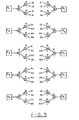
- Figures 1 A and 1B show two nets each permitting bidirectional communication between two sets of two devices. In each case the net is separable into two mutually converse nets. (The net of Figure 1 B allows four concurrent paths between the groups while the net of Figure 1 A allows only two concurrent paths.)
- a net is said to be self-converse if for each directed path connecting a pair of endpoints the converse path exists. The net then has the property that the source address of each path endpoint is the destination address from the other endpoint.
- a two-terminal system component e.g., store, processor, 1-0 device, or system
- a two-terminal system component can be shared by two or more devices connected via structurally similar trees of arbiter and selector switches.
- Figure 2 illustrates the case for four sharing devices 0 1 , O2, D 3 , and 0 4 ,
- Figure 3 shows the general interconnection using trees of arbiters and selectors which have the property of being mutually converse networks.
- any number of devices can be connected in this fashion. Since device identifications are generated internally in the arbiter trees and used internally in the selector trees, the spanning tree need not be unique; indeed, it may be determined for convenience in placement of the switches or for minimization of the total length of the interconnecting wires.
- Figures 4A and 4B show two arrangements for five devices.
- a typical application is a set of computer terminals sharing a central processor or database. Messages may consist of one or more characters.
- the central system will maintain a queue for each terminal in which messages from that terminal are assembled. All conflicting requests for lines will be resolved by the arbiter trees. Ordering of messages is automatic. Thus the central system has no need for a program to poll terminals or to represent configurations, such functions being accommodated in a decentralized manner in the switches.
- a hierarchical network similar to that familiar from telephone switching can be constructed by using a number of networks of the type shown in Figure 3. If each network is broken at a device, the output and input connections can be used as the input and output of the network. The resulting two-terminal network can then be used as one of the devices of a similar network at a higher level, thus giving a hierarchical structure.
- Another class of networks of interest is those networks where each device is connected symmetrically to some of the other devices.
- the networks of this form which give the maximum number of concurrent paths are those in which the device outputs are each connected to the root node of a selector tree and the device inputs are each connected to the root node of an arbiter tree with the leaf nodes of the trees connected to each other in such a manner that the network is self-converse.
- An example of this type of network where each of five devices is connected to the other four is shown in Figure 5.
- Figure 5 An example of this type of network where each of five devices is connected to the other four is shown in Figure 5.
- This type of network is similar to conventional crossbars. If the trees used are not homogeneous, the shorter paths through the arbiter trees will have greater priority since under heavy loading an arbiter accepts messages alternately from its two inputs.
- the network of Figure 6 connects each device to its two neighbors giving a linear array of devices.
- Figure 7 shows the network associated with a device which can communicate with any of four neighbors. This interconnection gives a two dimensional array of devices.
- Figure 11 shows a network using the arbiter and selector trees of Figure 3 and the hexagonal connector of Figure 8 to connect a number of processor and store pairs with a global store and an input/output device.
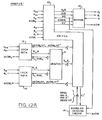
- the arbiter switch includes switch circuit 10, arbiter circuit 11, lock path circuits 12 and 13, address sending circuit 14 and buffer circuit 15.
- the arbiter switch receives message signals from two different stations or nodes, determines which of the messages is to be transmitted and then transmits that message through the arbiter switch, adding an address bit at the end of the message to indicate which of the two sending nodes transmitted the signal.
- the respective data signals are also received by corresponding lock path circuits 12 and 13 as will be more thoroughly described below.
- that circuit transmits a request signal R x A to arbiter circuit 11 and when such a request has been accepted, arbiter circuit 11 sends a set signal S x to switch circuit 10 to set switch circuit 10 to that path for subsequent passage of the transmitted message to buffer 15.
- address sending circuit 14 adds an address bit to the end of the message to indicate which previous node transmitted the message.
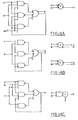
- Lock path switches 12 and 13 are identical and are represented in Figure 12B. The only difference between the two lock path circuits is that they receive signals from a different station or node.
- the data signals d x0 and d x1 are received by respective NAND gates 20 where they are NANDED with an inhibiting signal.
- the outputs of the respective NAND gates are then NANDED together to form a data request signal d o R which is sent through a C-element circuit 22 that also receives an inverted internal acknowledge end of message signal.
- the output of C-element 22 is transmitted to C-element circuit 23 which also receives a true internal acknowledge end of message signal.
- the output of C-element 22 is sent to NAND circuit 24 which transmits the request signal R x A.
- C-element 23 also receives the set to path x signal S . and transmits an acknowledge end of message signal AEOM x .
- C-element circuits 22 and 23 are illustrated in Figures 14A and 14C respectively.
- Arbiter circuit 11 of Figure 12A is illustrated in Figure 12C.
- a latch formed of gates 25 and 26, respectively receives the request path to arbiter signals R 0 A and R 1 A along with an initializing signal.
- the output of this latch is two inverted locked arbiter signals AL' o , and AL' 1 . These signals are delayed by inverters 27 before presentation to a latch formed by gates 28 and 29.
- This latch also receives a signal from metastability detector 30 that has as inputs locked arbiter signal AL 0 and the inverse thereof, AL' o .
- the detector determines whether both inputs are in the high or low signal regions or whether the two signals are in between the high and low regions indicating that the latch is in the metastable state.
- gates 28 One output from gates 28 is the set to path zero signal, So, which is transmitted to switch 10 of Figure 12A along with set to path one signal S 1 from gate 29.
- Gates 28 and 29 respectively also produce inhibit data signals INHD 0 and INHD 1 which are transmitted with the corresponding set to path signals back to their related lock path switches.
- Switch 10 of Figure 12A will now be described in relation to Figure 12D.
- the respective sets of data signals d oo , d 01 and d 10 , d 11 are received by the circuit along with a send signal, an inhibit acknowledge signal as well as the set to path signals So and S 1 .
- These signals and an inverted clear signal CL' are received by a variety of NAND gates 30 to gate one of the two data sets or the address bit to NAND gates 32 generating the outputs d 0 O and d 1 Q.
- one or the other of the end of message signals EOM 0 , EOM 1 is selectively gated to end of message signal EOMQ by way of AND gates 31 and OR gate 32.
- Gates 31 also provide gated inverted EOM x signals which along with an acknowledge end of message signal AEOM are transmitted by NAND gate 33 as an inverted clear signal CL'.
- the switch provides for transmission of an acknowledge signal in the other direction as either of the acknowledge signals A 0 or A 1 by way of AND gates 34 depending upon the state of the set to path signals So and S 1 and the inverted inhibit acknowledge signal.
- an incoming internal acknowledge end of message signal is gated out by gates 35 as the true and inverse of either of AEOM 0 INT or AEOM 1 INT, depending again upon the state of the set to path signals So and S,.
- Address sending circuit 14 in Figure 12A is illustrated in Figure 12E. As indicated therein, this circuit receives the acknowledge end of message signal AEOM, the internal acknowledge signal AQ and the inverted clear signal CL' and in return generates the true and complement of the inhibit A signal as well as the send signal and the internal AEOM signal.
- the incoming AQ and AEOM signals are received by NAND gate 36 along with the inverted internal AEOM signal to generate the inverted address sent signal that is transmitted to C-element 37 and 38 which are illustrated in detail in Figures 14G and 14B.
- the inverted clear signal is also received by C-element 37.
- AND gate 39 receives the AEOM signal, the inverted clear signal CL' and the inverted internal AEOM signal to generate the inhibit acknowledge signal INHA as well as the inverse thereof.
- C-element 38 generates the send signal, which along with the INHA signal, is required for transmission of the address bit to buffer 15 of Figure 12A.
- Buffer element 15 of Figure 12A will now be described in relation to Figure 12F.
- This element is a two cell queue which provides storage for one bit of data and allows pipelining of data through the switches.
- the buffer will not allow data to be transmitted from the switch until it can be accepted by the receiving circuit and will not accept data unless there is room to store it.
- the buffer circuit is also provided with a circuit to delay the end of message signal EOM so that it will not propagate past the last bit of the data preceding it.
- internal data signals d o O and d 1 Q are received by corresponding C-elements 40, which also have as inputs the FULL' signal from gate 44 and which generate the internal data signals d 0 l and d 1 l.
- the inverses of these last two signals are supplied to gate 41 which in turn sends back internal acknowledge signal AQ.
- the internal data signals are in turn received by corresponding C-elements 42, the outputs of which are the transmitted data signals do and d 1 .
- the inverses of these two data signals are supplied to AND gate 44 to generate the FULL' signal sent to C-elements 40.
- the inverted initialization signal from inverter 45 is also an input to gate 44.
- the acknowledge signal from the next station or node is inverted by inverter 43 and transmitted to C-elements 42.
- the internal end of message signal EOMQ is supplied to C-element 50 which also receives a FULL' signal from gate 44, the inverted acknowledge signal from inverter 43, and the inverted clear signal CL'.
- latch 50 supplies the inverted internal end of message signal EOMI' to C-element 51 which also receives a FULL' signal from gate 44 and the inverted acknowledge signal from inverter 43.
- the output of C-element 51 is the end of message signal EOM which is transmitted to the next station or node.
- C-elements 40, 42, 50 and 51 are illustrated in detail in Figures 14B, 14D, 14E and 14F respectively.
- the selector switch includes address circuit 60, clear circuit 61, as well as a pair of switch and buffer circuits 62 each with an end of message EOM circuit.
- the function of the selector switch is to receive messages having a leading address from another station or node and to determine to which of two stations or nodes the message is to be transmitted depending upon the first bit in the address.
- the first bit in the address sets the circuit path and the rest of the bits are transmitted to the same node until completion of the message is detected and the circuit is cleared. The first bit will then be removed from the address of the following message and the selector path set accordingly.
- Address circuit 60 of Figure 13A is illustrated in Figure 13B and includes two sets of C-elements 66 and 67.
- C-elements 66 receive the incoming data signals do and d 1 by way of NAND gates 65.
- NAND gates 65 also receive an inverted reset signal from gate 68.
- C-elements 66 receive a reset signal and transmit set signals ASET o and ASET, to C-elements 67.
- C-elements 67 receive an inverted clear signal and transmit the set to path signals So and S 1 to the respective switch and buffer circuits 62 of Figure 13A.
- Gate 68 transmits a reset signal to the clear circuit in the selector switch.
- Clear circuit 61 of Figure 13A is illustrated in Figure 13C and includes C-element 74 which receives a gated acknowledge end of message signal AEOM . , from the node to which the message has been transmitted. C-element 74 also receives a reset signal from address circuit 60 of Figure 13A and produces the acknowledge end of message signal, AEOM, which is transmitted to the station or node from which the message was received. This signal is also sent to NAND gate 75 as is the true output of AND/NAND gate 76. The output of gate 75 is an inverted clear signal that is transmitted to address circuit 60 of Figure 13A.
- Switch and buffer circuits 62 are illustrated in Figure 13D and each serves as a two cell queue with storage for one bit of data. It is this queue which allows pipelining of data through the switches.
- This buffer will not be described in detail except to say that it receives the incoming data signals do and d, as well as the end of message signal EOM and, upon selection of a particular buffer by signals So and S,, transmits those signals as data signals d x0 , d X1 and end of message signal EOM x .
- C-elements 70, 71, 72 and 73 are illustrated in Figures 14H, 14D, 14E and 14F respectively.
- the present invention is directed toward a digital communication network wherein messages may be sent from a source to a destination through the network.
Landscapes
- Engineering & Computer Science (AREA)
- Theoretical Computer Science (AREA)
- Computer Hardware Design (AREA)
- Physics & Mathematics (AREA)
- General Engineering & Computer Science (AREA)
- General Physics & Mathematics (AREA)
- Mathematical Physics (AREA)
- Software Systems (AREA)
- Computing Systems (AREA)
- Computer Networks & Wireless Communication (AREA)
- Signal Processing (AREA)
- Data Exchanges In Wide-Area Networks (AREA)
- Multi Processors (AREA)
- Small-Scale Networks (AREA)
- Mobile Radio Communication Systems (AREA)
Priority Applications (1)
| Application Number | Priority Date | Filing Date | Title |
|---|---|---|---|
| AT80301252T ATE3791T1 (de) | 1979-05-02 | 1980-04-18 | Digitale nachrichtennetze mit von der geschwindigkeit unabhaengigen schaltern. |
Applications Claiming Priority (2)
| Application Number | Priority Date | Filing Date | Title |
|---|---|---|---|
| US06/035,314 US4307446A (en) | 1979-05-02 | 1979-05-02 | Digital communication networks employing speed independent switches |
| US35314 | 1979-05-02 |
Publications (2)
| Publication Number | Publication Date |
|---|---|
| EP0018755A1 EP0018755A1 (en) | 1980-11-12 |
| EP0018755B1 true EP0018755B1 (en) | 1983-06-15 |
Family
ID=21881892
Family Applications (1)
| Application Number | Title | Priority Date | Filing Date |
|---|---|---|---|
| EP80301252A Expired EP0018755B1 (en) | 1979-05-02 | 1980-04-18 | Digital communication networks employing speed independent switches |
Country Status (6)
| Country | Link |
|---|---|
| US (1) | US4307446A (https=) |
| EP (1) | EP0018755B1 (https=) |
| JP (1) | JPS55147854A (https=) |
| AT (1) | ATE3791T1 (https=) |
| DE (1) | DE3063744D1 (https=) |
| IE (1) | IE49451B1 (https=) |
Families Citing this family (51)
| Publication number | Priority date | Publication date | Assignee | Title |
|---|---|---|---|---|
| US4488151A (en) * | 1981-12-10 | 1984-12-11 | Burroughs Corporation | Arbiter switch for a concurrent network of processors |
| US4814979A (en) * | 1981-04-01 | 1989-03-21 | Teradata Corporation | Network to transmit prioritized subtask pockets to dedicated processors |
| JPS588359A (ja) * | 1981-07-07 | 1983-01-18 | バロース コーポレーション | 還元プロセサの同時処理回路網および処理方法 |
| SE440766B (sv) * | 1981-10-09 | 1985-08-19 | Facit Ab | Pappersmatningsanordning |
| US4965825A (en) | 1981-11-03 | 1990-10-23 | The Personalized Mass Media Corporation | Signal processing apparatus and methods |
| US7831204B1 (en) | 1981-11-03 | 2010-11-09 | Personalized Media Communications, Llc | Signal processing apparatus and methods |
| USRE47642E1 (en) | 1981-11-03 | 2019-10-08 | Personalized Media Communications LLC | Signal processing apparatus and methods |
| US4498133A (en) * | 1981-12-10 | 1985-02-05 | Burroughs Corp. | Selector switch for a concurrent network of processors |
| EP0097351A3 (en) * | 1982-06-21 | 1986-02-26 | Nec Corporation | Router unit and routing network for determining an output port by detecting a part of an input packet |
| US4491945A (en) * | 1982-06-25 | 1985-01-01 | At&T Bell Laboratories | Fast packet switch |
| US4494230A (en) * | 1982-06-25 | 1985-01-15 | At&T Bell Laboratories | Fast packet switching system |
| US4482996A (en) * | 1982-09-02 | 1984-11-13 | Burroughs Corporation | Five port module as a node in an asynchronous speed independent network of concurrent processors |
| US4484325A (en) * | 1982-09-02 | 1984-11-20 | Burroughs Corporation | Four way selector switch for a five port module as a node asynchronous speed independent network of concurrent processors |
| GB8333519D0 (en) * | 1983-12-16 | 1984-01-25 | Gen Electric Co Plc | Data signal switching systems |
| JPS61223924A (ja) * | 1985-03-29 | 1986-10-04 | Hitachi Ltd | 信号伝送方式 |
| US4706080A (en) * | 1985-08-26 | 1987-11-10 | Bell Communications Research, Inc. | Interconnection of broadcast networks |
| US4730250A (en) * | 1985-09-03 | 1988-03-08 | Ncr Corporation | Local area network processing system |
| US4763329A (en) * | 1986-02-10 | 1988-08-09 | Techlan, Inc. | Modular data routing system |
| US5093916A (en) * | 1988-05-20 | 1992-03-03 | International Business Machines Corporation | System for inserting constructs into compiled code, defining scoping of common blocks and dynamically binding common blocks to tasks |
| US5033087A (en) * | 1989-03-14 | 1991-07-16 | International Business Machines Corp. | Method and apparatus for the automatic determination of phonological rules as for a continuous speech recognition system |
| US5790198A (en) | 1990-09-10 | 1998-08-04 | Starsight Telecast, Inc. | Television schedule information transmission and utilization system and process |
| US7210159B2 (en) * | 1994-02-18 | 2007-04-24 | Starsight Telecast, Inc. | System and method for transmitting and utilizing electronic programs guide information |
| US5619274A (en) * | 1990-09-10 | 1997-04-08 | Starsight Telecast, Inc. | Television schedule information transmission and utilization system and process |
| IE920032A1 (en) * | 1991-01-11 | 1992-07-15 | Marconi Gec Ltd | Parallel processing apparatus |
| US5404461A (en) * | 1991-03-29 | 1995-04-04 | International Business Machines Corp. | Broadcast/switching apparatus for executing broadcast/multi-cast transfers over unbuffered asynchronous switching networks |
| US5250943A (en) | 1991-03-29 | 1993-10-05 | International Business Machines Corporation | GVT-NET--A Global Virtual Time Calculation Apparatus for Multi-Stage Networks |
| US5365228A (en) * | 1991-03-29 | 1994-11-15 | International Business Machines Corporation | SYNC-NET- a barrier synchronization apparatus for multi-stage networks |
| US5321813A (en) * | 1991-05-01 | 1994-06-14 | Teradata Corporation | Reconfigurable, fault tolerant, multistage interconnect network and protocol |
| JP2571655B2 (ja) * | 1991-11-27 | 1997-01-16 | インターナショナル・ビジネス・マシーンズ・コーポレイション | プロトコル変換機構、交換ネットワーク及びコンピュータ・システム |
| US8352400B2 (en) | 1991-12-23 | 2013-01-08 | Hoffberg Steven M | Adaptive pattern recognition based controller apparatus and method and human-factored interface therefore |
| GB2279538A (en) * | 1993-06-24 | 1995-01-04 | Kim Philip Lyon | Binary data communication switch |
| US8793738B2 (en) | 1994-05-04 | 2014-07-29 | Starsight Telecast Incorporated | Television system with downloadable features |
| US6807558B1 (en) | 1995-06-12 | 2004-10-19 | Pointcast, Inc. | Utilization of information “push” technology |
| US5740549A (en) * | 1995-06-12 | 1998-04-14 | Pointcast, Inc. | Information and advertising distribution system and method |
| US20020178051A1 (en) | 1995-07-25 | 2002-11-28 | Thomas G. Scavone | Interactive marketing network and process using electronic certificates |
| US6264560B1 (en) | 1996-01-19 | 2001-07-24 | Sheldon F. Goldberg | Method and system for playing games on a network |
| US9530150B2 (en) | 1996-01-19 | 2016-12-27 | Adcension, Llc | Compensation model for network services |
| US5823879A (en) | 1996-01-19 | 1998-10-20 | Sheldon F. Goldberg | Network gaming system |
| US6138162A (en) * | 1997-02-11 | 2000-10-24 | Pointcast, Inc. | Method and apparatus for configuring a client to redirect requests to a caching proxy server based on a category ID with the request |
| US6173311B1 (en) | 1997-02-13 | 2001-01-09 | Pointcast, Inc. | Apparatus, method and article of manufacture for servicing client requests on a network |
| US6078847A (en) * | 1997-11-24 | 2000-06-20 | Hewlett-Packard Company | Self-organizing materials handling systems |
| US6442755B1 (en) | 1998-07-07 | 2002-08-27 | United Video Properties, Inc. | Electronic program guide using markup language |
| US7904187B2 (en) | 1999-02-01 | 2011-03-08 | Hoffberg Steven M | Internet appliance system and method |
| US6404441B1 (en) | 1999-07-16 | 2002-06-11 | Jet Software, Inc. | System for creating media presentations of computer software application programs |
| US6629149B1 (en) * | 1999-08-17 | 2003-09-30 | At&T Corp. | Network system and method |
| US6418526B1 (en) | 1999-11-15 | 2002-07-09 | Ncr Corporation | Method and apparatus for synchronizing nodes in massively parallel systems |
| US6519697B1 (en) | 1999-11-15 | 2003-02-11 | Ncr Corporation | Method and apparatus for coordinating the configuration of massively parallel systems |
| US6745240B1 (en) | 1999-11-15 | 2004-06-01 | Ncr Corporation | Method and apparatus for configuring massively parallel systems |
| US6412002B1 (en) | 1999-11-15 | 2002-06-25 | Ncr Corporation | Method and apparatus for selecting nodes in configuring massively parallel systems |
| JP4824306B2 (ja) * | 2004-12-22 | 2011-11-30 | 日本フェンオール株式会社 | 噴霧ノズルおよびこれを用いた噴霧消火ヘッド |
| US8775245B2 (en) | 2010-02-11 | 2014-07-08 | News America Marketing Properties, Llc | Secure coupon distribution |
Family Cites Families (11)
| Publication number | Priority date | Publication date | Assignee | Title |
|---|---|---|---|---|
| CH393423A (de) * | 1960-07-18 | 1965-06-15 | Bull Sa Machines | Anordnung zum Speichern und Verarbeiten von Informationen |
| US3252142A (en) * | 1962-09-10 | 1966-05-17 | Codamite Corp | Code receiver responsive to plural binary sub-group |
| GB1394432A (en) * | 1971-06-24 | 1975-05-14 | Plessey Co Ltd | Input-output arrangement for use in a data processing system |
| US3962706A (en) * | 1974-03-29 | 1976-06-08 | Massachusetts Institute Of Technology | Data processing apparatus for highly parallel execution of stored programs |
| US4153932A (en) * | 1974-03-29 | 1979-05-08 | Massachusetts Institute Of Technology | Data processing apparatus for highly parallel execution of stored programs |
| IT1012440B (it) * | 1974-05-16 | 1977-03-10 | Honeywell Inf Systems | Apparato di controllo dei canali di ingresso e uscita delle informa zioni di un calcolatore |
| JPS52130246A (en) * | 1976-04-24 | 1977-11-01 | Fujitsu Ltd | Memory access control system |
| US4041465A (en) * | 1976-04-27 | 1977-08-09 | International Telephone And Telegraph Corporation | Scanner-distributor apparatus for matrix system |
| US4041472A (en) * | 1976-04-29 | 1977-08-09 | Ncr Corporation | Data processing internal communications system having plural time-shared intercommunication buses and inter-bus communication means |
| US4071908A (en) * | 1977-03-17 | 1978-01-31 | Bell Telephone Laboratories, Incorporated | Adaptive polling technique |
| US4162534A (en) * | 1977-07-29 | 1979-07-24 | Burroughs Corporation | Parallel alignment network for d-ordered vector elements |
-
1979
- 1979-05-02 US US06/035,314 patent/US4307446A/en not_active Expired - Lifetime
-
1980
- 1980-04-15 JP JP5109380A patent/JPS55147854A/ja active Granted
- 1980-04-18 EP EP80301252A patent/EP0018755B1/en not_active Expired
- 1980-04-18 AT AT80301252T patent/ATE3791T1/de not_active IP Right Cessation
- 1980-04-18 DE DE8080301252T patent/DE3063744D1/de not_active Expired
- 1980-04-24 IE IE831/80A patent/IE49451B1/en unknown
Also Published As
| Publication number | Publication date |
|---|---|
| US4307446A (en) | 1981-12-22 |
| ATE3791T1 (de) | 1983-06-15 |
| JPS55147854A (en) | 1980-11-18 |
| EP0018755A1 (en) | 1980-11-12 |
| JPH0151108B2 (https=) | 1989-11-01 |
| IE49451B1 (en) | 1985-10-02 |
| DE3063744D1 (en) | 1983-07-21 |
| IE800831L (en) | 1980-11-02 |
Similar Documents
| Publication | Publication Date | Title |
|---|---|---|
| EP0018755B1 (en) | Digital communication networks employing speed independent switches | |
| EP0018754B1 (en) | Speed independent selector switch for digital communication networks | |
| EP0018756B1 (en) | Speed independent arbiter switch for digital communication networks | |
| US4933933A (en) | Torus routing chip | |
| EP3776231B1 (en) | Procedures for implementing source based routing within an interconnect fabric on a system on chip | |
| US5130977A (en) | Message routing | |
| EP0200780B1 (en) | Packet switched multiple queue nxm switch node and processing method | |
| US5140583A (en) | Message routing | |
| EP0198010B1 (en) | Packet switched multiport memory nxm switch node and processing method | |
| US6314487B1 (en) | Adaptive routing controller of a crossbar core module used in a crossbar routing switch | |
| US4482996A (en) | Five port module as a node in an asynchronous speed independent network of concurrent processors | |
| US5422881A (en) | Message encoding | |
| US4276611A (en) | Device for the control of data flows | |
| US4481623A (en) | Speed independent arbiter switch employing M-out-of-N codes | |
| EP0214840A2 (en) | Method of conflict resolution in a parallel processor network | |
| JPH05241947A (ja) | 分散クロスバー・スイッチ・アーキテクチャにおける交換接続の配列。 | |
| WO1984001079A1 (en) | Four way arbiter switch for a five port module as a node in an asynchronous speed-independent network of concurrent processors | |
| US4307378A (en) | Four-wire speed independent selector switch for digital communication networks | |
| US4763247A (en) | Multiprocessor system formed by microprocessor matrix | |
| US4484325A (en) | Four way selector switch for a five port module as a node asynchronous speed independent network of concurrent processors | |
| RU2018945C1 (ru) | Блок выбора направления обмена децентрализованной вычислительной системы | |
| KR940005025B1 (ko) | 패킷방식 다단 상호 접속망용 스위칭 소자 | |
| KR930007017B1 (ko) | 인터커넥션 네트워크 스위칭소자 | |
| JPS5829550B2 (ja) | プロセツサ間高速デ−タ転送方式 | |
| JPH0253983B2 (https=) |
Legal Events
| Date | Code | Title | Description |
|---|---|---|---|
| PUAI | Public reference made under article 153(3) epc to a published international application that has entered the european phase |
Free format text: ORIGINAL CODE: 0009012 |
|
| AK | Designated contracting states |
Designated state(s): AT BE CH DE FR GB IT LU NL SE |
|
| 17P | Request for examination filed |
Effective date: 19810113 |
|
| ITF | It: translation for a ep patent filed | ||
| GRAA | (expected) grant |
Free format text: ORIGINAL CODE: 0009210 |
|
| AK | Designated contracting states |
Designated state(s): AT BE CH DE FR GB IT LI LU NL SE |
|
| REF | Corresponds to: |
Ref document number: 3791 Country of ref document: AT Date of ref document: 19830615 Kind code of ref document: T |
|
| REF | Corresponds to: |
Ref document number: 3063744 Country of ref document: DE Date of ref document: 19830721 |
|
| ET | Fr: translation filed | ||
| PLBE | No opposition filed within time limit |
Free format text: ORIGINAL CODE: 0009261 |
|
| STAA | Information on the status of an ep patent application or granted ep patent |
Free format text: STATUS: NO OPPOSITION FILED WITHIN TIME LIMIT |
|
| 26N | No opposition filed | ||
| ITPR | It: changes in ownership of a european patent |
Owner name: FUSIONI;BURROUGHS DELAWARE INCORPORATED ( DETROIT |
|
| REG | Reference to a national code |
Ref country code: CH Ref legal event code: PFA Free format text: BURROUGHS CORPORATION (A DELAWARE CORPORATION) |
|
| REG | Reference to a national code |
Ref country code: GB Ref legal event code: 732 |
|
| NLS | Nl: assignments of ep-patents |
Owner name: BURROUGHS CORPORATION TE DETROIT, MICHIGAN, VER. S |
|
| PGFP | Annual fee paid to national office [announced via postgrant information from national office to epo] |
Ref country code: LU Payment date: 19920403 Year of fee payment: 13 |
|
| PGFP | Annual fee paid to national office [announced via postgrant information from national office to epo] |
Ref country code: BE Payment date: 19920512 Year of fee payment: 13 |
|
| PGFP | Annual fee paid to national office [announced via postgrant information from national office to epo] |
Ref country code: CH Payment date: 19920623 Year of fee payment: 13 |
|
| EPTA | Lu: last paid annual fee | ||
| PGFP | Annual fee paid to national office [announced via postgrant information from national office to epo] |
Ref country code: AT Payment date: 19930318 Year of fee payment: 14 |
|
| PGFP | Annual fee paid to national office [announced via postgrant information from national office to epo] |
Ref country code: SE Payment date: 19930322 Year of fee payment: 14 |
|
| PG25 | Lapsed in a contracting state [announced via postgrant information from national office to epo] |
Ref country code: LU Free format text: LAPSE BECAUSE OF NON-PAYMENT OF DUE FEES Effective date: 19930418 |
|
| ITTA | It: last paid annual fee | ||
| PG25 | Lapsed in a contracting state [announced via postgrant information from national office to epo] |
Ref country code: LI Effective date: 19930430 Ref country code: CH Effective date: 19930430 Ref country code: BE Effective date: 19930430 |
|
| PGFP | Annual fee paid to national office [announced via postgrant information from national office to epo] |
Ref country code: NL Payment date: 19930430 Year of fee payment: 14 |
|
| BERE | Be: lapsed |
Owner name: BURROUGHS CORP. Effective date: 19930430 |
|
| REG | Reference to a national code |
Ref country code: CH Ref legal event code: PL |
|
| PGFP | Annual fee paid to national office [announced via postgrant information from national office to epo] |
Ref country code: GB Payment date: 19940321 Year of fee payment: 15 |
|
| PGFP | Annual fee paid to national office [announced via postgrant information from national office to epo] |
Ref country code: FR Payment date: 19940412 Year of fee payment: 15 |
|
| PG25 | Lapsed in a contracting state [announced via postgrant information from national office to epo] |
Ref country code: AT Effective date: 19940418 |
|
| PG25 | Lapsed in a contracting state [announced via postgrant information from national office to epo] |
Ref country code: SE Effective date: 19940419 |
|
| PGFP | Annual fee paid to national office [announced via postgrant information from national office to epo] |
Ref country code: DE Payment date: 19940427 Year of fee payment: 15 |
|
| PG25 | Lapsed in a contracting state [announced via postgrant information from national office to epo] |
Ref country code: NL Effective date: 19941101 |
|
| NLV4 | Nl: lapsed or anulled due to non-payment of the annual fee | ||
| EUG | Se: european patent has lapsed |
Ref document number: 80301252.5 Effective date: 19941110 |
|
| PG25 | Lapsed in a contracting state [announced via postgrant information from national office to epo] |
Ref country code: GB Effective date: 19950418 |
|
| GBPC | Gb: european patent ceased through non-payment of renewal fee |
Effective date: 19950418 |
|
| PG25 | Lapsed in a contracting state [announced via postgrant information from national office to epo] |
Ref country code: FR Effective date: 19951229 |
|
| PG25 | Lapsed in a contracting state [announced via postgrant information from national office to epo] |
Ref country code: DE Effective date: 19960103 |
|
| REG | Reference to a national code |
Ref country code: FR Ref legal event code: ST |