EP0013102B1 - Power supply providing constant power output - Google Patents
Power supply providing constant power output Download PDFInfo
- Publication number
- EP0013102B1 EP0013102B1 EP79302888A EP79302888A EP0013102B1 EP 0013102 B1 EP0013102 B1 EP 0013102B1 EP 79302888 A EP79302888 A EP 79302888A EP 79302888 A EP79302888 A EP 79302888A EP 0013102 B1 EP0013102 B1 EP 0013102B1
- Authority
- EP
- European Patent Office
- Prior art keywords
- power
- voltage
- capacitor
- load resistance
- source
- Prior art date
- Legal status (The legal status is an assumption and is not a legal conclusion. Google has not performed a legal analysis and makes no representation as to the accuracy of the status listed.)
- Expired
Links
Images
Classifications
-
- H—ELECTRICITY
- H04—ELECTRIC COMMUNICATION TECHNIQUE
- H04M—TELEPHONIC COMMUNICATION
- H04M19/00—Current supply arrangements for telephone systems
- H04M19/001—Current supply source at the exchanger providing current to substations
- H04M19/008—Using DC/DC converters
-
- H—ELECTRICITY
- H02—GENERATION; CONVERSION OR DISTRIBUTION OF ELECTRIC POWER
- H02M—APPARATUS FOR CONVERSION BETWEEN AC AND AC, BETWEEN AC AND DC, OR BETWEEN DC AND DC, AND FOR USE WITH MAINS OR SIMILAR POWER SUPPLY SYSTEMS; CONVERSION OF DC OR AC INPUT POWER INTO SURGE OUTPUT POWER; CONTROL OR REGULATION THEREOF
- H02M7/00—Conversion of AC power input into DC power output; Conversion of DC power input into AC power output
- H02M7/02—Conversion of AC power input into DC power output without possibility of reversal
- H02M7/04—Conversion of AC power input into DC power output without possibility of reversal by static converters
- H02M7/05—Capacitor coupled rectifiers
Definitions
- This invention relates generally to power supplies and, more specifically to power supplies for deriving from a substantially rectangular wave source substantially constant average power in a load resistance over a broad range of resistance values.
- a major design consideration is one of limiting power dissipation.
- a subscriber loop carrier system must supply DC current to the telephone equipment which it serves. Dissipation becomes a significant concern in a system wherein many loops are powered within a small volume, such as a field-located cabinet. In addition, dissipation increases reserve battery capacity requirements and cost. Therefore a nondissipative DC power supply that provides constant average power into a variable resistance load allows for effective power load planning and equipment design.
- the article discloses circuit arrangements and corresponding component values for obtaining a relatively constant power output over a range of load resistance values.
- the range is somewhat limited since, for example, only a three octave change in resistance values about a preselected operating point results in ⁇ 35 percent power variations.
- the "constant" power mode is established by tuning an inductor and capacitor pair to the frequency of a sinusoidal input source so operation is sensitive to component variations of this pair.
- a power supply as aforesaid comprises capacitor means adapted to be serially connected to said source for accumulating charge, converter means serially connected to said capacitor means for developing a uni-directional current, and inductor means connected effectively in series between said converter means and said load resistance when connected to said supply, for maintaining said current through a path including said load resistance, wherein, in use of the power supply, the power dissipated in said load resistance is substantially constant for load resistance values less than 1/4FC, where F is the frequency of said source and C is the capacitance of said capacitor means.
- an improved power supply provides constant power to a variable resistance load.
- the power supply comprises: an AC portion including an alternating polarity source feeding a serially connected capacitor; and a DC portion including rectifier means serially connected to the capacitor and an inductor interposed between the rectifier means and the load resistance.
- Constant power is delivered to the load whenever the load resistance does not exceed a parameter fixed by the capacitor value and the repetition rate of the source. Since the capacitor charges to full voltage before the end of a half- period of the source and the output voltage varies directly with charging time whereas the output current varies inversely with respect to charging time, the product of voltage and current remains constant.
- a particularly novel feature of the power supply implemented in accordance with the present invention is that, although the source is alternating in polarity at a nominal repetition rate and an inductor and capacitor pair control circuit operation, the supply is essentially insensitive to repetition rate changes and component variations. Since the principle of operation does not rely on resonance of the pair, the component values and repetition rate are chosen so that all reasonably anticipated variations do not affect circuit performance.
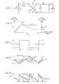
- a power supply is shown as wherein an alternating polarity, square-wave source 11 is connected across input terminals 1 and 2.
- Capacitor 12 is serially connected between terminals 2 and 4.
- the anode of diode 13 is connected to terminal 4 and the cathode of diode 13 is connected to terminal 6.
- Diode 14 has its anode connected to terminal 5 and its cathode to terminal 4.
- Diode 15 is connected between terminals 3 and 6, with the anode connected to terminal 3.
- Diode 16 is connected between terminals 3 and 5, with the cathode connected to terminal 3.
- Inductor 17 is serially connected between terminals 6 and 7.
- Square-wave source 11 is symmetric and operates at a repetition frequency designated by f.
- Capacitor 12 has a value designated by C.
- the first mode produces a constant average output voltage supplied to load resistance 18 whenever R L is greater than R F .
- power output is inversely proportional to R L .
- the second mode exhibits constant average power delivered to load resistance 18, and this occurs for values of R L less than R F .
- R L decreases from its maximum value to R F
- the load current increases whereas the load voltage decreases inversely with respect to the current.
- the current-voltage product therefore remains constant.
- Fig. 1 shows that V o is measured at terminal 7 relative to terminal 5 as I o flows from terminal 7 to 5.
- P o is the average power dissipated in resistance 18.
- the mode characterised by constant average output voltage and associated variable output power delivered to load R L is exhibited for output current values between 0 and a current designated I F .
- the constant power and corresponding variable voltage mode exist for all output current values greater than IF. In this mode, the proportionality relation between the voltage and current is displayed.
- V F designates the constant voltage resulting from mode one operation, then, for example: an output current of 21 F yields an output voltage of V F /2; a current of 41 F results in a voltage of V F /4; and so forth.
- the constant power in this second mode is given by the product V F I F .
- Fig. 3, 4 and 5 show voltage wavefroms that are useful in describing circuit operation.
- the square-wave generated by source 11 is given in Fig. 3.
- Fig. 4 shows the instantaneous steady-state voltage across capacitor 12 (terminal 2 relative to 4 in Fig. 1)
- Fig. 5 depicts the instantaneous steady-state voltage across the output of bridge 20 (terminal 6 relative to 5 in Fig. 1).
- the waveforms shown in both Fig. 4 and Fig. 5 are dependent on load resistance 18 and curves for three specific values of R L are plotted to facilitate description.
- the first mode of operation which exhibits constant average output voltage, occurs whenever R L is greater than R F .
- the voltage output from bridge 20 varies linearly and equally about the voltage V F level supplied by source 11.
- V F the average voltage into inductor 17, which functions primarily as a low-frequency filter in this mode.
- the second mode of operation exhibits constant average output power whenever R L is less than R F .
- R L R F
- capacitor 12 just charges to the maximum or minimum possible voltage V F or -V F , respectively, at the end of each half-cycle.
- the capacitor charges linearly between -V F and V F (or V F and -V F ), so from basic circuit considerations relating accumulated charge to capacitor value and voltage.
- the parameter a is a duty factor and represents the ratio of capacitor 12 charging time to the half-cycle time of source 11. Thus current conduction through capacitor 12 occurs with a duty factor of ⁇ . Furthermore, the average output voltage decreases and is determined by the percentage of time that capacitor 12 conducts, so the average output voltage is given by Finally, from equations (3) and (4), and the average output power is given by
- V F 48 V.
Landscapes
- Engineering & Computer Science (AREA)
- Signal Processing (AREA)
- Rectifiers (AREA)
- Dc-Dc Converters (AREA)
- Control Of Electrical Variables (AREA)
- Devices For Supply Of Signal Current (AREA)
- Direct Current Feeding And Distribution (AREA)
Applications Claiming Priority (2)
| Application Number | Priority Date | Filing Date | Title |
|---|---|---|---|
| US05/974,377 US4245294A (en) | 1978-12-29 | 1978-12-29 | Power supply providing constant power output |
| US974377 | 1978-12-29 |
Publications (2)
| Publication Number | Publication Date |
|---|---|
| EP0013102A1 EP0013102A1 (en) | 1980-07-09 |
| EP0013102B1 true EP0013102B1 (en) | 1983-02-16 |
Family
ID=25521960
Family Applications (1)
| Application Number | Title | Priority Date | Filing Date |
|---|---|---|---|
| EP79302888A Expired EP0013102B1 (en) | 1978-12-29 | 1979-12-13 | Power supply providing constant power output |
Country Status (6)
| Country | Link |
|---|---|
| US (1) | US4245294A (enExample) |
| EP (1) | EP0013102B1 (enExample) |
| JP (1) | JPS55123707A (enExample) |
| CA (1) | CA1131700A (enExample) |
| DE (1) | DE2964872D1 (enExample) |
| ES (1) | ES487295A1 (enExample) |
Families Citing this family (9)
| Publication number | Priority date | Publication date | Assignee | Title |
|---|---|---|---|---|
| US4408269A (en) * | 1982-06-18 | 1983-10-04 | Zenith Radio Corporation | Balanced power supply with polarized capacitors |
| US4600982A (en) * | 1984-02-22 | 1986-07-15 | Rolm Corporation | Low power consuming AC to DC converter |
| US4748551A (en) * | 1986-12-22 | 1988-05-31 | Peroxidation Systems, Inc. | Constant current supply for a varying resistance |
| US4901217A (en) * | 1987-12-01 | 1990-02-13 | Apple Computer, Inc. | Digital input power supply and method |
| US5191261A (en) * | 1991-06-11 | 1993-03-02 | Purus, Inc. | Switching power supply for high-voltage flash lamps |
| US5416416A (en) * | 1992-02-24 | 1995-05-16 | Bisher; Roger C. | Method and apparatus for testing an auxiliary power system |
| US5448155A (en) * | 1992-10-23 | 1995-09-05 | International Power Devices, Inc. | Regulated power supply using multiple load sensing |
| AU2389001A (en) * | 1999-12-22 | 2001-07-03 | Adc Telecommunications Israel Ltd. | Remote line feeding |
| US11565104B1 (en) * | 2021-08-09 | 2023-01-31 | Yossi Gross | Magnetically-driven reciprocating intravascular blood pump |
Family Cites Families (7)
| Publication number | Priority date | Publication date | Assignee | Title |
|---|---|---|---|---|
| US3001120A (en) * | 1957-10-16 | 1961-09-19 | Baldwin Piano Co | Power supplies |
| US3304440A (en) * | 1963-12-26 | 1967-02-14 | Bell Telephone Labor Inc | Pulse shaping circuit |
| US3286185A (en) * | 1965-10-22 | 1966-11-15 | Combustion Eng | Flame detector system responsive to spike produced by townsend avalanche of glow discharge tube |
| DE1563121A1 (de) * | 1966-07-05 | 1970-01-29 | Werner Ansorge | Gleichrichterschaltungen mit Zenerdioden |
| JPS4943127A (enExample) * | 1972-09-01 | 1974-04-23 | ||
| JPS51127343A (en) * | 1975-04-28 | 1976-11-06 | Hitachi Ltd | Controlling transducer |
| US4131939A (en) * | 1977-03-30 | 1978-12-26 | Day Ralph D | Constant current power supply |
-
1978
- 1978-12-29 US US05/974,377 patent/US4245294A/en not_active Expired - Lifetime
-
1979
- 1979-12-11 CA CA341,634A patent/CA1131700A/en not_active Expired
- 1979-12-13 EP EP79302888A patent/EP0013102B1/en not_active Expired
- 1979-12-13 DE DE7979302888T patent/DE2964872D1/de not_active Expired
- 1979-12-27 ES ES487295A patent/ES487295A1/es not_active Expired
- 1979-12-28 JP JP17393879A patent/JPS55123707A/ja active Granted
Also Published As
| Publication number | Publication date |
|---|---|
| US4245294A (en) | 1981-01-13 |
| EP0013102A1 (en) | 1980-07-09 |
| CA1131700A (en) | 1982-09-14 |
| JPH0376114B2 (enExample) | 1991-12-04 |
| ES487295A1 (es) | 1980-08-01 |
| JPS55123707A (en) | 1980-09-24 |
| DE2964872D1 (en) | 1983-03-24 |
Similar Documents
| Publication | Publication Date | Title |
|---|---|---|
| US4641233A (en) | AC to DC converter with voltage regulation | |
| US6094036A (en) | Electrical power supply with low-loss inrush current limiter and step-up converter circuit | |
| GB2324916A (en) | Pulse load averaging power converter | |
| JPH07143751A (ja) | 電源回路 | |
| EP0129181A2 (en) | DC-DC converter | |
| NZ209570A (en) | Switching regulator | |
| KR880000870B1 (ko) | 전원회로 | |
| EP0013102A1 (en) | Power supply providing constant power output | |
| US8472211B2 (en) | Single stage power conversion unit with circuit to smooth and holdup DC output voltage | |
| US6396724B1 (en) | Charge-pumped DC bias supply | |
| AU2018388865B2 (en) | Wide range power supply for use in meters and other devices | |
| US5239453A (en) | DC to DC converter employing a free-running single stage blocking oscillator | |
| US4263644A (en) | Current limiter for switched DC-to-DC converter | |
| EP0964504B1 (en) | Switching power source apparatus | |
| US4591962A (en) | Regulated power supply for rapid no-load to full-load transitions | |
| US6473322B2 (en) | AC-DC converter | |
| JPH09504679A (ja) | スイッチモード電源 | |
| US5745357A (en) | Regulator circuit and multi-output switching power unit using the regulator circuit | |
| US5434769A (en) | Multi-phase adaptable AC-DC converter | |
| JP3406851B2 (ja) | 電源装置 | |
| JP2656850B2 (ja) | 交流信号監視回路 | |
| JPH05308733A (ja) | 充電回路方式及び充電装置 | |
| JPH0412791Y2 (enExample) | ||
| US5089949A (en) | High efficiency passive component voltage converter | |
| US6188207B1 (en) | Switching power supply |
Legal Events
| Date | Code | Title | Description |
|---|---|---|---|
| PUAI | Public reference made under article 153(3) epc to a published international application that has entered the european phase |
Free format text: ORIGINAL CODE: 0009012 |
|
| AK | Designated contracting states |
Designated state(s): BE DE FR GB IT NL |
|
| 17P | Request for examination filed |
Effective date: 19801222 |
|
| ITF | It: translation for a ep patent filed | ||
| GRAA | (expected) grant |
Free format text: ORIGINAL CODE: 0009210 |
|
| AK | Designated contracting states |
Designated state(s): BE DE FR GB IT NL |
|
| REF | Corresponds to: |
Ref document number: 2964872 Country of ref document: DE Date of ref document: 19830324 |
|
| ET | Fr: translation filed | ||
| ITTA | It: last paid annual fee | ||
| PGFP | Annual fee paid to national office [announced via postgrant information from national office to epo] |
Ref country code: GB Payment date: 19951020 Year of fee payment: 17 |
|
| PGFP | Annual fee paid to national office [announced via postgrant information from national office to epo] |
Ref country code: DE Payment date: 19951108 Year of fee payment: 17 |
|
| PGFP | Annual fee paid to national office [announced via postgrant information from national office to epo] |
Ref country code: FR Payment date: 19951110 Year of fee payment: 17 Ref country code: BE Payment date: 19951110 Year of fee payment: 17 |
|
| PGFP | Annual fee paid to national office [announced via postgrant information from national office to epo] |
Ref country code: NL Payment date: 19951230 Year of fee payment: 17 |
|
| PG25 | Lapsed in a contracting state [announced via postgrant information from national office to epo] |
Ref country code: GB Effective date: 19961213 |
|
| PG25 | Lapsed in a contracting state [announced via postgrant information from national office to epo] |
Ref country code: BE Effective date: 19961231 |
|
| BERE | Be: lapsed |
Owner name: WESTERN ELECTRIC CY INCORP. Effective date: 19961231 |
|
| PG25 | Lapsed in a contracting state [announced via postgrant information from national office to epo] |
Ref country code: NL Effective date: 19970701 |
|
| GBPC | Gb: european patent ceased through non-payment of renewal fee |
Effective date: 19961213 |
|
| PG25 | Lapsed in a contracting state [announced via postgrant information from national office to epo] |
Ref country code: FR Effective date: 19970829 |
|
| NLV4 | Nl: lapsed or anulled due to non-payment of the annual fee |
Effective date: 19970701 |
|
| PG25 | Lapsed in a contracting state [announced via postgrant information from national office to epo] |
Ref country code: DE Effective date: 19970902 |
|
| REG | Reference to a national code |
Ref country code: FR Ref legal event code: ST |
|
| PLBE | No opposition filed within time limit |
Free format text: ORIGINAL CODE: 0009261 |
|
| STAA | Information on the status of an ep patent application or granted ep patent |
Free format text: STATUS: NO OPPOSITION FILED WITHIN TIME LIMIT |