EP0012919B1 - Schaltungsanordnung zum Herabsetzen der Freiwerdezeit eines Thyristors - Google Patents
Schaltungsanordnung zum Herabsetzen der Freiwerdezeit eines Thyristors Download PDFInfo
- Publication number
- EP0012919B1 EP0012919B1 EP19790105075 EP79105075A EP0012919B1 EP 0012919 B1 EP0012919 B1 EP 0012919B1 EP 19790105075 EP19790105075 EP 19790105075 EP 79105075 A EP79105075 A EP 79105075A EP 0012919 B1 EP0012919 B1 EP 0012919B1
- Authority
- EP
- European Patent Office
- Prior art keywords
- thyristor
- circuit arrangement
- reducing
- recovery time
- diode
- Prior art date
- Legal status (The legal status is an assumption and is not a legal conclusion. Google has not performed a legal analysis and makes no representation as to the accuracy of the status listed.)
- Expired
Links
- 238000011084 recovery Methods 0.000 title claims 2
- 239000003990 capacitor Substances 0.000 claims description 8
- 230000003068 static effect Effects 0.000 description 2
- 239000002800 charge carrier Substances 0.000 description 1
- 230000006866 deterioration Effects 0.000 description 1
- 230000001681 protective effect Effects 0.000 description 1
Images
Classifications
-
- H—ELECTRICITY
- H03—ELECTRONIC CIRCUITRY
- H03K—PULSE TECHNIQUE
- H03K17/00—Electronic switching or gating, i.e. not by contact-making and –breaking
- H03K17/04—Modifications for accelerating switching
- H03K17/0403—Modifications for accelerating switching in thyristor switches
-
- H—ELECTRICITY
- H02—GENERATION; CONVERSION OR DISTRIBUTION OF ELECTRIC POWER
- H02M—APPARATUS FOR CONVERSION BETWEEN AC AND AC, BETWEEN AC AND DC, OR BETWEEN DC AND DC, AND FOR USE WITH MAINS OR SIMILAR POWER SUPPLY SYSTEMS; CONVERSION OF DC OR AC INPUT POWER INTO SURGE OUTPUT POWER; CONTROL OR REGULATION THEREOF
- H02M1/00—Details of apparatus for conversion
- H02M1/08—Circuits specially adapted for the generation of control voltages for semiconductor devices incorporated in static converters
Definitions
- the present application relates to a circuit arrangement for reducing the release time of a thyristor to which a rectifier is connected in anti-parallel.
- the invention has for its object to improve a circuit arrangement of the type mentioned in such a way that the release time is noticeably improved compared to the solution with an anti-parallel diode.
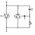
- the invention is characterized in that the rectifier is a further thyristor, that an RC element is connected in parallel in such a way that a connection of the resistor is connected to the anode and a connection of the capacitor to the cathode, and that a diode is provided, whose anode is connected to the connection point of resistor and capacitor and whose cathode is connected to the control connection of the further thyristor.
- an RC element provided as a protective circuit for the first thyristor is used as the RC element.
- the thyristor 1 hereinafter referred to as the first thyristor, is switched on, for example, in a branch of a DC chopper or a converter.
- the first thyristor 1 has the further thyristor 2, hereinafter referred to as the second thyristor, connected in anti-parallel. In terms of its data, it can be identical to the first thyristor 1 or can also have a lower power.
- An RC element which consists of a capacitor 3 and a resistor 4, is connected in parallel with the second thyristor 2.
- the capacitor 3 is connected to the cathode and the resistor 4 to the anode of the second thyristor 2.
- the anode of a diode 5 is connected to the connection point between capacitor 3 and resistor 4, the cathode of which is connected to the control connection of the second thyristor 2.
- the positive voltage rises to approximately 10 or a few 10V until the ignition at the thyristor 2, and then drops to the static forward voltage drop of approximately 1.5 to 2.0V within 10 or more microseconds.
- the release time is favorably influenced or reduced.
- the reverse current flowing through the thyristor 1 ceases. If the ignition delay time of the thyristor 2 is correspondingly long, a gentle decay of the reverse current in the thyristor 1 can be achieved.
- the thyristor 2 and the diode 5 are protected against steep voltage peaks by the capacitor 3. Excessive stress on the diode 5 and the base cathode path of the thyristor 2 is thus avoided.
- An RC combination can be provided as an RC combination, which must be provided in some circuits to protect the thyristor 1 against steep voltage and current edges.
- a common RC circuit for a medium-sized thyristor for example, has values of approximately 10 ohms, 0.25 p, F. With such a circuit arrangement, a reduction in the release time could be achieved by approximately 15% compared to the use of a normal anti-parallel diode.
Landscapes
- Engineering & Computer Science (AREA)
- Power Engineering (AREA)
- Dc-Dc Converters (AREA)
- Power Conversion In General (AREA)
- Thyristor Switches And Gates (AREA)
Description
- Die vorliegende Anmeldung bezieht sich auf eine Schaltungsanordnung zum Herabsetzen der Freiwerdezeit eines Thyristors, dem ein Gleichrichterantiparallelgeschaltet ist.
- Bei Gleichstromstellern, Umrichtern usw. mit Thyristoren werden diesen zum Umkommutieren des Stroms sogenannte Freilaufdioden antiparallelgeschaltet, die einen Energieausgleich im Steller- oder Umrichtersystem innerhalb des durch die Stellfrequenz oder Umrichfrequenz vorgegebenen Zeitraums möglich machen. Beim Umkommutieren des Stroms liegt damit am Thyristor eine Sperrspannung in Rückwärtsrichtung an, die gleich dem Spannungsabfall der Diode ist. Dieser Spannungsabfall kann dynamisch etwa 10 V für die Dauer von einigen Mikrosekunden betragen und geht dann in den statischen Wert von ca. 1,5...2,0 V über. Diese geringe Gegenspannung am Thyristor bringt im Vergleich zu einer negativen Sperrspannung von mindestens 100 V eine drastische Verschlechterung der Freiwerdezeit des Thyristors mit sich.
- Der Erfindung liegt die Aufgabe zugrunde, eine Schaltungsanordnung der eingangs erwähnten Art so zu verbessern, daß die Freiwerdezeit gegenüber der Lösung mit einer antiparallelgeschalteten Diode spürbar verbessert wird.
- Die Erfindung ist dadurch gekennzeichnet, daß der Gleichrichter ein weiterer Thyristor ist, daß diesem ein RC-Glied derart parallelgeschaltet ist, daß ein Anschluß des Widerstands mit der Anode und ein Anschluß des Kondensators mit der Katode verbunden ist, und daß eine Diode vorgesehen ist, deren Anode mit dem Verbindungspunkt von Widerstand und Kondensator und deren Katode mit dem Steueranschluß des weiteren Thyristors verbunden ist. Vorteilhafterweise wird als RC-Glied ein als Schutzschaltung für den ersten Thyristor vorgesehenes RC-Glied verwendet.
- In der Figur ist ein Ausführungsbeispiel der Erfindung dargestellt. Der Thyristor 1, im folgenden als erster Thyristor bezeichnet, ist zum Beispiel in einem Zweig eines Gleichstromstellers oder eines Umrichters eingeschaltet. Dem ersten Thyristor 1 ist der weitere Thyristor 2, im folgenden als zweiter Thyristor bezeichnet, antiparallelgeschaltet. Er kann in seinen Daten dem ersten Thyristor 1 identisch sein oder auch kleinere Leistung aufweisen. Dem zweiten Thyristor 2 ist ein RC-Glied parallelgeschaltet, das aus einem Kondensator 3 und einem Widerstand 4 besteht. Der Kondensator 3 ist mit der Katode und der Widerstand 4 mit der Anode des zweiten Thyristors 2 verbunden. Mit dem Verbindungspunkt zwischen Kondensator 3 und Widerstand 4 ist die Anode einer Diode 5 verbunden, deren Katode am Steueranschluß des zweiten Thyristors 2 liegt.
- Zur Erläuterung der Wirkungsweise sei angenommen, daß die am ersten Thyristor 1 anliegende Spannung von positiven Werten Kommend durch Null gegen negative Werte geht und der Strom abkommutiert wird. Beim Abriß des Rückstroms baut sich somit am Thyristor 1 eine negative Spannung auf, die zu einem Abbau der im Thyristor 1 gespeicherten Ladungsträger führt. Entsprechend dem Spannungsanstieg gegen negative Werte fließt ein Strom über den Widerstand 4 und die Diode 5 in den Steuereingang des zweiten Thyristors 2. Erreicht dieser strom den zum Zünden des Thyristors 2 erforderlichen Wert, so wird dieser leitend und kann den zum Energieausgleich in der Steller- oder Umrichterschaltung notwendigen Strom führen. Im Normalfall steigt die positive Spannung bis zur Zündung am Thyristor 2 auf ca. 10 oder einige 10V an, um dann innerhalb von 10 und mehr Mikrosekunden auf den statischen Durchlaßspannungsabfall von ca. 1,5...2,0 V abzufallen. Im Vergleich zur Schaltung mit antiparalleler Diode steht hier somit am Thyristor 1 eine höhere, langsamer abfallende Spannung in Sperrichtung an, wodurch die Freiwerdezeit günstig beeinflußt beziehungsweise kleiner wird. Entsprechend der Strom- übernahme durch den zweiten Thyristor 2 hört der durch den Thyristor 1 fließende Rückstrom auf. Ist die Zündverzugszeit des Thyristors 2 entsprechend groß, läßt sich ein sanftes Abklingen des Rückstroms im Thyristor 1 erreichen.
- Der Thyristor 2 und die Diode 5 sind gegen steile Spannungsspitzen durch den Kondensator 3 geschützt. Damit wird eine übermäßige Beanspruchung der Diode 5 und der Basis-Katodenstrecke des Thyristors 2 vermieden.
- Als RC-Kombination kann eine RC-Kombination vorgesehen werden, die zum Schutz des Thyristors 1 gegen steile Spannungs- und Stromflanken in manchen Schaltungen vorgesehen sein muß. Eine übliche RC-Beschaltung für einen mittelgroßen Thyristor hat zum Beispiel Werte von ca. 10 Ohm, 0,25 p,F. Mit einer solchen Schaltungsanordnung ließ sich gegenüber der Verwendung einer normalen antipärallelgeschalteten Diode eine Verkürzung der Freiwerdezeit um ca. 15% erreichen.
Claims (2)
Applications Claiming Priority (2)
| Application Number | Priority Date | Filing Date | Title |
|---|---|---|---|
| DE19782856780 DE2856780A1 (de) | 1978-12-29 | 1978-12-29 | Schaltungsanordnung zum herabsetzen der freiwerdezeit eines thyristors |
| DE2856780 | 1978-12-29 |
Publications (2)
| Publication Number | Publication Date |
|---|---|
| EP0012919A1 EP0012919A1 (de) | 1980-07-09 |
| EP0012919B1 true EP0012919B1 (de) | 1983-08-24 |
Family
ID=6058711
Family Applications (1)
| Application Number | Title | Priority Date | Filing Date |
|---|---|---|---|
| EP19790105075 Expired EP0012919B1 (de) | 1978-12-29 | 1979-12-10 | Schaltungsanordnung zum Herabsetzen der Freiwerdezeit eines Thyristors |
Country Status (3)
| Country | Link |
|---|---|
| EP (1) | EP0012919B1 (de) |
| JP (1) | JPS5592568A (de) |
| DE (1) | DE2856780A1 (de) |
Family Cites Families (6)
| Publication number | Priority date | Publication date | Assignee | Title |
|---|---|---|---|---|
| US3213349A (en) * | 1962-04-18 | 1965-10-19 | Gen Electric | Protective control circuits |
| DE1255206B (de) * | 1964-05-25 | 1967-11-30 | Wiener Starkstromwerke Ges M B | Loeschschaltung fuer Gasentladungs- oder Halbleiter-Thyratron |
| GB1174086A (en) * | 1967-02-17 | 1969-12-10 | Westinghouse Brske And Signal | Improvements to Capacitor-Commutated Circuits |
| FR1551207A (de) * | 1967-11-16 | 1968-12-27 | ||
| US3614531A (en) * | 1970-08-18 | 1971-10-19 | Joseph V Oswald | Shunt means for protecting a power supply against back emf |
| US3943430A (en) * | 1974-06-20 | 1976-03-09 | Mitsubishi Denki Kabushi Kaisha | Circuitry for reducing thyristor turn-off times |
-
1978
- 1978-12-29 DE DE19782856780 patent/DE2856780A1/de not_active Withdrawn
-
1979
- 1979-12-10 EP EP19790105075 patent/EP0012919B1/de not_active Expired
- 1979-12-25 JP JP17022179A patent/JPS5592568A/ja active Pending
Also Published As
| Publication number | Publication date |
|---|---|
| JPS5592568A (en) | 1980-07-14 |
| DE2856780A1 (de) | 1980-07-17 |
| EP0012919A1 (de) | 1980-07-09 |
Similar Documents
| Publication | Publication Date | Title |
|---|---|---|
| DE69508644T2 (de) | Halbleiter-Leistungsmodul und -Leistungswandlervorrichtung | |
| DE2834512C2 (de) | Umformer mit ausschaltbaren Thyristoren | |
| DE2211828A1 (de) | Statische Gleichstromschalter-Anordnung | |
| DE69921607T2 (de) | Verfahren zum Entfernen von Kurzschluss-Abschnitten einer Solarzelle | |
| CH660266A5 (de) | Thyristoreinrichtung mit durch licht steuerbaren thyristoren. | |
| DE2506021A1 (de) | Ueberspannungs-schutzschaltung fuer hochleistungsthyristoren | |
| DE2223376B2 (de) | Schutzschaltungsanordnung für einen Schalttransistor im induktiven Lastkreis | |
| DE2654419A1 (de) | Schaltungsanordnung zur spannungsbegrenzung | |
| DE3032328A1 (de) | Ueberstromschutzschaltung | |
| DE68924493T2 (de) | Schutzschaltung gegen transiente Überspannungen. | |
| DE102016118039A1 (de) | Solarmodul, Photovoltaikanlage und Verfahren zur Spannungsbegrenzung | |
| DE2724741C3 (de) | Schutzbeschaltung für jeweils ein Stromrichterventil | |
| DE3215589C2 (de) | ||
| DE2461583C2 (de) | Schaltung zur Reduzierung der Einschaltverluste eines Leistungstransistors | |
| DE102021006486A1 (de) | Kurzschlussdetektor und leistungswandler | |
| DE2063436C2 (de) | Stromrichteranordnung | |
| DE102020207668A1 (de) | Dämpfungsschaltung und stromrichter | |
| EP0012919A1 (de) | Schaltungsanordnung zum Herabsetzen der Freiwerdezeit eines Thyristors | |
| WO2020011331A1 (de) | Modularer multilevel-stromrichter mit unterschiedlichen submodultypen | |
| EP0009225A1 (de) | Schutzbeschaltung | |
| DE3230910C2 (de) | ||
| EP0177779B1 (de) | Schaltungsanordnung mit einer Speiseschaltung zur Speisung eines Lastwiderstandes | |
| DE2632381A1 (de) | Wechselrichterschaltung | |
| DE3009709A1 (de) | Schalteranordnung zum abschalten hoher gleichstroeme unter hoher spannung | |
| DE3700788A1 (de) | Blockierbarer nichtmechanischer unterbrecher fuer einen wechselstromkreis mit einer induktiven last |
Legal Events
| Date | Code | Title | Description |
|---|---|---|---|
| PUAI | Public reference made under article 153(3) epc to a published international application that has entered the european phase |
Free format text: ORIGINAL CODE: 0009012 |
|
| AK | Designated contracting states |
Designated state(s): FR GB IT SE |
|
| 17P | Request for examination filed |
Effective date: 19801208 |
|
| ITF | It: translation for a ep patent filed | ||
| GRAA | (expected) grant |
Free format text: ORIGINAL CODE: 0009210 |
|
| AK | Designated contracting states |
Designated state(s): FR GB IT SE |
|
| ET | Fr: translation filed | ||
| PGFP | Annual fee paid to national office [announced via postgrant information from national office to epo] |
Ref country code: SE Payment date: 19831130 Year of fee payment: 5 |
|
| PGFP | Annual fee paid to national office [announced via postgrant information from national office to epo] |
Ref country code: FR Payment date: 19831227 Year of fee payment: 5 |
|
| PLBE | No opposition filed within time limit |
Free format text: ORIGINAL CODE: 0009261 |
|
| STAA | Information on the status of an ep patent application or granted ep patent |
Free format text: STATUS: NO OPPOSITION FILED WITHIN TIME LIMIT |
|
| 26N | No opposition filed | ||
| PG25 | Lapsed in a contracting state [announced via postgrant information from national office to epo] |
Ref country code: SE Effective date: 19841211 |
|
| GBPC | Gb: european patent ceased through non-payment of renewal fee | ||
| PG25 | Lapsed in a contracting state [announced via postgrant information from national office to epo] |
Ref country code: FR Free format text: LAPSE BECAUSE OF NON-PAYMENT OF DUE FEES Effective date: 19850830 |
|
| REG | Reference to a national code |
Ref country code: FR Ref legal event code: ST |
|
| PG25 | Lapsed in a contracting state [announced via postgrant information from national office to epo] |
Ref country code: GB Effective date: 19881118 |
|
| EUG | Se: european patent has lapsed |
Ref document number: 79105075.0 Effective date: 19851007 |