EP0010783A1 - Verfahren und Vorrichtung zum Erkennen der Anwesenheit eines oder mehrerer Mehrfrequenzcodezeichen in einem PCM-Signal - Google Patents
Verfahren und Vorrichtung zum Erkennen der Anwesenheit eines oder mehrerer Mehrfrequenzcodezeichen in einem PCM-Signal Download PDFInfo
- Publication number
- EP0010783A1 EP0010783A1 EP79200473A EP79200473A EP0010783A1 EP 0010783 A1 EP0010783 A1 EP 0010783A1 EP 79200473 A EP79200473 A EP 79200473A EP 79200473 A EP79200473 A EP 79200473A EP 0010783 A1 EP0010783 A1 EP 0010783A1
- Authority
- EP
- European Patent Office
- Prior art keywords
- signal
- samples
- pcm
- circuit
- accumulator
- Prior art date
- Legal status (The legal status is an assumption and is not a legal conclusion. Google has not performed a legal analysis and makes no representation as to the accuracy of the status listed.)
- Granted
Links
Images


Classifications
-
- H—ELECTRICITY
- H04—ELECTRIC COMMUNICATION TECHNIQUE
- H04Q—SELECTING
- H04Q1/00—Details of selecting apparatus or arrangements
- H04Q1/18—Electrical details
- H04Q1/30—Signalling arrangements; Manipulation of signalling currents
- H04Q1/44—Signalling arrangements; Manipulation of signalling currents using alternate current
- H04Q1/444—Signalling arrangements; Manipulation of signalling currents using alternate current with voice-band signalling frequencies
- H04Q1/45—Signalling arrangements; Manipulation of signalling currents using alternate current with voice-band signalling frequencies using multi-frequency signalling
- H04Q1/457—Signalling arrangements; Manipulation of signalling currents using alternate current with voice-band signalling frequencies using multi-frequency signalling with conversion of multifrequency signals into digital signals
- H04Q1/4575—Signalling arrangements; Manipulation of signalling currents using alternate current with voice-band signalling frequencies using multi-frequency signalling with conversion of multifrequency signals into digital signals which are transmitted in digital form
Definitions
- the invention relates to a method and a device for detecting the presence or absence of one or more of a fixed number of certain frequencies within a pulse code modulated signal, the signal to be investigated being multiplied by each of two reference series for each of the said certain frequencies.
- the method and device are applied in telecommunication exchanges in detecting voice-frequency signalling signals contained in a telecommunication channel itself or in a separate signalling channel.
- the object of the invention is to provide a method and device which, starting from those described in US patent 3882283, yield a more efficient use of the equipment and more reliable detection.
- the invention is based on the insight that twice as many samples of the signal to be detected are available as are needed for reliable detection according to the sampling theorem, so that half of the samples can remain unused.
- the method according to the invention is characterized in that sets of two subsequent ones of the samples available for detection within a PCM signal are alternately used and not used for detection.
- An improvement of the said method consists in that the number of samples used for detection is equal or practically equal to half a whole multiple of the number of samples which, at the sampling frequency, represent one period of the difference frequency of the said certain frequencies.
- the invention provides a device for carrying out the first-mentioned method, which device comprises the means of comparing alternately two samples of a first PCM-signal and two samples of a second PCM-signal with the samples of the reference series, and means for feeding the results of this comparison alternately in the same rhythm to the detection device.
- a device for carrying out the first-mentioned method which device comprises the means of comparing alternately two samples of a first PCM-signal and two samples of a second PCM-signal with the samples of the reference series, and means for feeding the results of this comparison alternately in the same rhythm to the detection device.
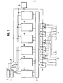
- the block diagram of Fig. 1 comprises an input memory 1 for the incoming series of signals of a first PCM-signal A and an input memory 2 for ar incoming series of signals of a second PCM-signal B.
- a switch 3 provides for throughconnection of the series of signals.
- a square-wave oscillator 4 controls switch 3 in such a way that each time two samples from each of the input memories 1 and 2 are alternately switched through.
- Square-wave oscillator 4 is synchronized with the incoming signal in the known manner.
- the signal coming from switch 3 is fed via a common input 5 to each of discriminators 6, each of the latter being suitable for the discrimination of one frequency.
- the construction and operation of a discriminator 6 will afterwards be described with the aid of Fig. 2.
- Each discriminator 6 is equipped with an input 7 for reception of the square-wave signal of oscillator 4.
- the discriminators each have an output 8, at which alternately appears an accumulated value of a comparison of a sine sample of signals A and B respectively, and an output 9 at which appears a similar value of the comparison with a cosine sample.
- Outputs 8 and 9 are connected to a known comparator circuit 10.
- the outputs of comparator circuit 10 are conducted to switches 11, which according to the invention are controlled by oscillator 4.
- switches 11, which according to the invention are controlled by oscillator 4.
- On each of the six outputs 12 a signal may now appear which is representative of each of the frequencies found in signal A respectively. If for instance a two-out-of-six signalling code is applied, only two of the outputs 12 will be simultaneously "high” for example and the other four "low".
- On outputs 13 an identical situation is found for the frequencies encountered within signal B.
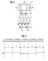
- Fig. 2 presents a more detailed diagram of discriminator 6 of Fig. 1. .
- Each of these discriminators is suitable for one of the six frequencies.
- the signal from input 5 is fed to a known detection device 14, which signal is multiplied by a sine reference series of the frequency concerned stored in a buffer 15 and by a cosine reference series of the frequency concerned.
- the result of both multiplications is fed via two switches 17 to two of four accumulators 18, 19, 20 and 21.
- the results of the multiplication of signal A by the sine reference series are stored in accumulator 18; those for signal B in accumulator 19.
- the results of the multiplication of the signals from PCM-signals A and B respectively are accumulated in accumulators 20 and 21 with the cosine reference series.
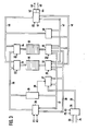
- Fig. 3 shows a preferred embodiment of a device according to the invention for detecting signalling signals in each of the eight channels of two frames.
- PCM-samples for signalling are offered in a 125 ⁇ s frame comprising 32 time slots.
- the incoming PCM-samples with MFC signalling are distributed in the exchange over time slots T0, T4, T8, T12, T16, T20, T2A and T28. So there are 8 MFC signalling channels with a channel spacing of 15.6 us.
- the detection device is controlled by the central processing unit of the telephone exchange.
- the operation of this central processing unit is of no importance in explaining the invention and can therefore be left out of consideration.
- An MFC detection device for both the outgoing and the incoming direction will comprise 12 x 2 reference series and 6 x 2 accumulators.
- Fig. 3 shows such a device in which a PCM-signal A is received on an input 23 and a PCM-signal B on an input 24, of which PCM-signals each time the part containing the MFC-signals is fed to input bus 26 by the input selector.
- Input selector 25 operates under the control of a synchronization signal FS, which becomes "high" each time during the eight time slots TO - T28, and of a synchronization signal AS, which according to the invention changes its sign every two frames and as a result alternately feeds two of each of the time slots with signalling information from PCM-signal A and two of each of the time slots with signalling information from PCM-signal B to input bus 26.
- a synchronization signal FS which becomes "high" each time during the eight time slots TO - T28
- AS which according to the invention changes its sign every two frames and as a result alternately feeds two of each of the time slots with signalling information from PCM-signal A and two of each of the
- the synchronization characters FS and AS are direct derivatives of the signal received by the telephone exchange. The formation of these signals is generally known and will not be discussed here.
- Circuit 27 processes each incoming signal in the same way without distinguishing between channels.
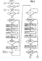
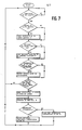
- Fig. 6 is a flowchart of circuit 27, which consists of part of a microprocessor circuit.
- Input control circuit 28 is realized together with circuit 27 by means of a microprocessor; the two circuits have been drawn separately in order to emphasize the two different functions.
- Circuit 28 sees to it that at the right moment the right data is released to enable circuit 27 to carry out an operation. Circuit 28 is linked to the frame by means of synchronization signals FS and AS (Fig. 4).
- the reference series are stored in a programmable read-only memory (PROM), reference series buffer 29. As stated above, it contains 12 sine reference series and 12 cosine reference series.
- PROM programmable read-only memory
- circuit 27 comprises an accumulator 30 for signal A, in which the data are accumulated in the known manner after having been processed by circuit 27.
- RAM random access memory
- an input address bus 36 has been provided via which input control circuit 28 can feed address information to buffer 29 and selectors 31 and 34.
- circuits 27 and 28 can give orders to each other and to buffer 29 and selectors 32 and 35.
- the data to be processed are exchanged via a bidirectional input data bus 38.
- the circuit also incorporates an output processing circuit 40 for processing the data stored in the accumulators, and an output control circuit 41.
- Circuits 40 and 41 have been jointly embodied as one microprocessor and have been drawn separately because of their different functions. The functional operation of circuits 40 and 41 is illustrated by Figures 8 and 9 respectively.
- the data processed by circuit 40 can be fed to the central processing unit of the telephone exchange via an output bus 42.
- connections are provided by means of an output address bus 46, an output control bus 47 and a bidi- rectionaloutput data bus 48.
- Input control circuit 28 and output control circuit 41 can both effect changes in each of the status words associated with each of the eight time slots. This presents the possibility of an exchange of messages between circuits 28 aid 41.
- Circuit 28 waits for signal AS to change its sign. As appears from Fig. 3, this causes accumulator 30 to become accessible when signal AS is “high” or causes accumulator 33 to become accessible when signal AS is “low”. After the change of signal AS, circuit 28 waits till signal FS also becomes “high”, after which it is investigated whether the status word associated with time slot TO contains a detection order.
- the circuit waits till signal FS is "high" again for the next time slot that may contain MFC signalling.
- circuit 28 determines the starting address of the character bits in the reference series buffer and the starting address of the accumulated values for time slot TO in accumulator 30 or 33, depending on signal AS.
- Circuit 28 now regularly places an address on address bus 36 and orders processing circuit 27 via control bus 37 to collect the data from the accumulator, to add them to the result of the multiplication of the samples from input selector 25 and reference series buffer 29 respectively, and to place the final result in the accumulator. This process is repeated for each of the six frequencies that may be found in each time slot (see Fig. 6). Next, the same process is applied to the signals in time slots T4, T8, T12, T16, T20, T24 and T28.
- Fig. 4 shows, two frames of one PCM-channel are processed in succession each time, and then two frames of a second PCM-channel.
- the results of the first PCM-channel are stored in accumulator 30 each time via data selector 32, and the results of the second PCM-channel are fed to accumulator 33 via data selector 35.
- the number of samples of each time slot required equals half a multiple of the number of samples by means of which a 120 Hz period (the fixed difference frequency between the MFC frequencies) can be defined.
- a 120 Hz period is defined by 67 samples.
- Two periods are defined by 134 samples and three periods by 200 samples.
- control circuit 28 changes the status word stored in accumulators 30 and 33 and discontinues the processing of the signals received.
- the central processing unit (not included in the Figures) has given a detection order via input 43 (Fig. 7) and control circuit 41 concludes from the status word in the accumulator concerned that the detection procedure is completed, the results of the accumulation are fed to the working store of processing circuit 40 under the control of the control circuit. According to flowchart 8 these data are now processed. The moduli of the values of the cosine accumulator and those of the sine accumulator of one frequency are compared with each other.
- the smaller of the two values is multiplied by a factor 1, - or 1.
- the multiplication factor depends on the ratio between the largest and the smallest accumulator value. The largest value and the smallest value multiplied by the factor are now added together.
Landscapes
- Engineering & Computer Science (AREA)
- Computer Networks & Wireless Communication (AREA)
- Time-Division Multiplex Systems (AREA)
- Digital Transmission Methods That Use Modulated Carrier Waves (AREA)
Applications Claiming Priority (2)
| Application Number | Priority Date | Filing Date | Title |
|---|---|---|---|
| NLAANVRAGE7809213,A NL177169B (nl) | 1978-09-08 | 1978-09-08 | Inrichting om de aanwezigheid vast te stellen van een of meer van een aantal frequenties in pulscode-gemoduleerde signalen. |
| NL7809213 | 1978-09-08 |
Publications (2)
| Publication Number | Publication Date |
|---|---|
| EP0010783A1 true EP0010783A1 (de) | 1980-05-14 |
| EP0010783B1 EP0010783B1 (de) | 1981-11-04 |
Family
ID=19831513
Family Applications (1)
| Application Number | Title | Priority Date | Filing Date |
|---|---|---|---|
| EP79200473A Expired EP0010783B1 (de) | 1978-09-08 | 1979-08-29 | Verfahren und Vorrichtung zum Erkennen der Anwesenheit eines oder mehrerer Mehrfrequenzcodezeichen in einem PCM-Signal |
Country Status (4)
| Country | Link |
|---|---|
| US (1) | US4279017A (de) |
| EP (1) | EP0010783B1 (de) |
| DE (1) | DE2961258D1 (de) |
| NL (1) | NL177169B (de) |
Cited By (1)
| Publication number | Priority date | Publication date | Assignee | Title |
|---|---|---|---|---|
| GB2130051A (en) * | 1982-11-10 | 1984-05-23 | Wescom | Telecommunication supervision system |
Families Citing this family (5)
| Publication number | Priority date | Publication date | Assignee | Title |
|---|---|---|---|---|
| FR2485843B1 (fr) * | 1980-06-25 | 1986-11-07 | Cit Alcatel | Recepteur numerique de frequences |
| GB2095013B (en) * | 1981-03-18 | 1984-10-17 | Philips Electronic Associated | Multi-tone sequential call signal detector |
| US4901244A (en) * | 1985-01-25 | 1990-02-13 | Szeto Lai Wan M | Apparatus for, and method of, analyzing signals |
| US4730257A (en) * | 1985-01-25 | 1988-03-08 | Szeto Lai Wan M | Apparatus for analyzing signals, to obtain parameters of constituents |
| JPH0884161A (ja) * | 1994-09-13 | 1996-03-26 | Fuji Electric Co Ltd | バイフェーズ符号を用いたシリアル通信装置用の受信検知回路装置 |
Citations (1)
| Publication number | Priority date | Publication date | Assignee | Title |
|---|---|---|---|---|
| FR2180901A1 (de) * | 1972-04-17 | 1973-11-30 | Nederlanden Staat |
Family Cites Families (4)
| Publication number | Priority date | Publication date | Assignee | Title |
|---|---|---|---|---|
| CA984068A (en) * | 1972-08-10 | 1976-02-17 | Alexander D. Proudfoot | Method and apparatus for detecting the presence of signal components of predetermined frequency in a multi-frequency signal |
| US3962645A (en) * | 1974-11-06 | 1976-06-08 | General Electric Company | Tone frequency detecting circuit |
| FR2299769A1 (fr) * | 1975-01-31 | 1976-08-27 | Telecommunications Sa | Procede d'application |
| NL170797C (nl) * | 1975-11-18 | 1982-12-16 | Nederlanden Staat | Inrichting voor het detecteren van een signaal. |
-
1978
- 1978-09-08 NL NLAANVRAGE7809213,A patent/NL177169B/xx not_active IP Right Cessation
-
1979
- 1979-08-21 US US06/068,406 patent/US4279017A/en not_active Expired - Lifetime
- 1979-08-29 EP EP79200473A patent/EP0010783B1/de not_active Expired
- 1979-08-29 DE DE7979200473T patent/DE2961258D1/de not_active Expired
Patent Citations (1)
| Publication number | Priority date | Publication date | Assignee | Title |
|---|---|---|---|---|
| FR2180901A1 (de) * | 1972-04-17 | 1973-11-30 | Nederlanden Staat |
Non-Patent Citations (1)
| Title |
|---|
| 1972 INTERNATIONAL ZURICH SEMINAR ON INTEGRATED SYSTEMS FOR SPEECH VIDEO AND DATA COMMUNICATIONS. 15-17th March 1972 Zurich (CH) F. PELLANDINI: "Methodes et moyens pour l' elaboration digitale de signaux analogiques", pages A3(1)-A3(13) * Page A3 (7), right-hand column, line 49 - page A3 (8); left-hand column, line 19 * * |
Cited By (1)
| Publication number | Priority date | Publication date | Assignee | Title |
|---|---|---|---|---|
| GB2130051A (en) * | 1982-11-10 | 1984-05-23 | Wescom | Telecommunication supervision system |
Also Published As
| Publication number | Publication date |
|---|---|
| NL7809213A (nl) | 1980-03-11 |
| EP0010783B1 (de) | 1981-11-04 |
| NL177169B (nl) | 1985-03-01 |
| US4279017A (en) | 1981-07-14 |
| DE2961258D1 (en) | 1982-01-14 |
Similar Documents
| Publication | Publication Date | Title |
|---|---|---|
| US4686672A (en) | TDMA communications apparatus having adaptive burst duration | |
| US4071711A (en) | Telephone subscriber distribution system | |
| KR880701048A (ko) | 스위칭 시스템 | |
| US4450557A (en) | Switching network for use in a time division multiplex system | |
| GB2024565A (en) | Bit-by-bit time -division digital switching network | |
| US6385259B1 (en) | Composite code match filters | |
| DE2918539C2 (de) | Paket-Übertragungssystem für Ton- und Datensignale | |
| EP0010783B1 (de) | Verfahren und Vorrichtung zum Erkennen der Anwesenheit eines oder mehrerer Mehrfrequenzcodezeichen in einem PCM-Signal | |
| EP0523571A1 (de) | Gerät für Fehlererkennungskode und Einrichtung mit binärer Pseudozufallsfolge maximaler Länge | |
| GB1566164A (en) | Method and apparatus for recognising and producing separated signals from multifrequency coded input signals | |
| US4507783A (en) | Error detection circuitry for digital systems | |
| KR880700581A (ko) | 단일 라인 전화통신 시스템 | |
| CA1268868A (en) | Arrangement for processing received data in tdma communications system and method therefor | |
| EP0462689B1 (de) | Digitale Schaltung zum Multiplexen | |
| EP0301934B1 (de) | Zeit-Multiplex-Vermittlungssystem für Paketen verschiedener Länge | |
| HK14996A (en) | Digital filter | |
| JPH08181715A (ja) | 送受信装置 | |
| EP0078634B1 (de) | Koppelfeld zum Gebrauch in einem Zeitmultiplex-Vermittlungssystem | |
| US5371856A (en) | Transfer data storage system | |
| SU1075429A1 (ru) | Многоканальна система передачи двоичной информации с временным уплотнением | |
| JP2745901B2 (ja) | パケット交換方式 | |
| EP0183519B1 (de) | Datenübertragungsnetzwerk | |
| JP3029353B2 (ja) | 遠方監視制御装置 | |
| JPH0279536A (ja) | ポーリング・セレクティング装置 | |
| JPS5918916B2 (ja) | 多周波信号受信器 |
Legal Events
| Date | Code | Title | Description |
|---|---|---|---|
| PUAI | Public reference made under article 153(3) epc to a published international application that has entered the european phase |
Free format text: ORIGINAL CODE: 0009012 |
|
| 17P | Request for examination filed | ||
| AK | Designated contracting states |
Designated state(s): DE FR IT SE |
|
| ITCL | It: translation for ep claims filed |
Representative=s name: STUDIO MASSARI S.R.L. |
|
| DET | De: translation of patent claims | ||
| ITF | It: translation for a ep patent filed | ||
| GRAA | (expected) grant |
Free format text: ORIGINAL CODE: 0009210 |
|
| AK | Designated contracting states |
Designated state(s): DE FR IT SE |
|
| REF | Corresponds to: |
Ref document number: 2961258 Country of ref document: DE Date of ref document: 19820114 |
|
| PGFP | Annual fee paid to national office [announced via postgrant information from national office to epo] |
Ref country code: DE Payment date: 19840802 Year of fee payment: 6 |
|
| PGFP | Annual fee paid to national office [announced via postgrant information from national office to epo] |
Ref country code: FR Payment date: 19840831 Year of fee payment: 6 |
|
| PGFP | Annual fee paid to national office [announced via postgrant information from national office to epo] |
Ref country code: SE Payment date: 19840930 Year of fee payment: 6 |
|
| PG25 | Lapsed in a contracting state [announced via postgrant information from national office to epo] |
Ref country code: SE Effective date: 19880830 |
|
| PG25 | Lapsed in a contracting state [announced via postgrant information from national office to epo] |
Ref country code: FR Free format text: LAPSE BECAUSE OF NON-PAYMENT OF DUE FEES Effective date: 19890428 |
|
| REG | Reference to a national code |
Ref country code: FR Ref legal event code: ST |
|
| PG25 | Lapsed in a contracting state [announced via postgrant information from national office to epo] |
Ref country code: DE Effective date: 19890701 |
|
| EUG | Se: european patent has lapsed |
Ref document number: 79200473.1 Effective date: 19890510 |
|
| PLBE | No opposition filed within time limit |
Free format text: ORIGINAL CODE: 0009261 |
|
| STAA | Information on the status of an ep patent application or granted ep patent |
Free format text: STATUS: NO OPPOSITION FILED WITHIN TIME LIMIT |