EP0004787B1 - Heated semiconductor bonding tool - Google Patents
Heated semiconductor bonding tool Download PDFInfo
- Publication number
- EP0004787B1 EP0004787B1 EP79300576A EP79300576A EP0004787B1 EP 0004787 B1 EP0004787 B1 EP 0004787B1 EP 79300576 A EP79300576 A EP 79300576A EP 79300576 A EP79300576 A EP 79300576A EP 0004787 B1 EP0004787 B1 EP 0004787B1
- Authority
- EP
- European Patent Office
- Prior art keywords
- bonding tool
- heater
- tool
- heated
- film
- Prior art date
- Legal status (The legal status is an assumption and is not a legal conclusion. Google has not performed a legal analysis and makes no representation as to the accuracy of the status listed.)
- Expired
Links
Images

Classifications
-
- H—ELECTRICITY
- H10—SEMICONDUCTOR DEVICES; ELECTRIC SOLID-STATE DEVICES NOT OTHERWISE PROVIDED FOR
- H10W—GENERIC PACKAGES, INTERCONNECTIONS, CONNECTORS OR OTHER CONSTRUCTIONAL DETAILS OF DEVICES COVERED BY CLASS H10
- H10W72/00—Interconnections or connectors in packages
- H10W72/071—Connecting or disconnecting
- H10W72/0711—Apparatus therefor
-
- H—ELECTRICITY
- H10—SEMICONDUCTOR DEVICES; ELECTRIC SOLID-STATE DEVICES NOT OTHERWISE PROVIDED FOR
- H10W—GENERIC PACKAGES, INTERCONNECTIONS, CONNECTORS OR OTHER CONSTRUCTIONAL DETAILS OF DEVICES COVERED BY CLASS H10
- H10W72/00—Interconnections or connectors in packages
- H10W72/071—Connecting or disconnecting
- H10W72/0711—Apparatus therefor
- H10W72/07141—Means for applying energy, e.g. ovens or lasers
-
- H—ELECTRICITY
- H10—SEMICONDUCTOR DEVICES; ELECTRIC SOLID-STATE DEVICES NOT OTHERWISE PROVIDED FOR
- H10W—GENERIC PACKAGES, INTERCONNECTIONS, CONNECTORS OR OTHER CONSTRUCTIONAL DETAILS OF DEVICES COVERED BY CLASS H10
- H10W72/00—Interconnections or connectors in packages
- H10W72/071—Connecting or disconnecting
- H10W72/075—Connecting or disconnecting of bond wires
- H10W72/07531—Techniques
-
- H—ELECTRICITY
- H10—SEMICONDUCTOR DEVICES; ELECTRIC SOLID-STATE DEVICES NOT OTHERWISE PROVIDED FOR
- H10W—GENERIC PACKAGES, INTERCONNECTIONS, CONNECTORS OR OTHER CONSTRUCTIONAL DETAILS OF DEVICES COVERED BY CLASS H10
- H10W72/00—Interconnections or connectors in packages
- H10W72/071—Connecting or disconnecting
- H10W72/075—Connecting or disconnecting of bond wires
- H10W72/07531—Techniques
- H10W72/07532—Compression bonding, e.g. thermocompression bonding
Definitions
- the invention relates to heated bonding tools and more especially to the heating elements of such tools.
- Such bonding tools are used in the manufacture of semiconductor devices to make electrical connections by attaching fine wires to electrodes or terminal pads on the semiconductor devices.
- Such tools may achieve bonding simply by the application of heat and pressure or may also use ultrasonic vibration.
- the heating elements In existing bonding tools the heating elements generally fall into one of two classes. Either the tool holder has a heating element embodied therein or the heating element is attached to the bonding tool proper.
- cartridge type heaters and wound wire heaters had to be large in comparison to the size of the bonding tool because the heat was transmitted through one or more air to heater surfaces. Attempts to silver solder or attach the prior art heaters to the bonding tool or bonding tool holder did not succeed because premature failure of the heating element rendered the expensive bonding tool or holder inoperable thus requiring expensive rework.
- Cartridge and wire wound mini heaters generate their heat at a point which is remote from the working tip of the bonding tool. This requires that the heater not only supply additional heat which is dissipated, but, that the heat be operated at a substantially higher temperature to overcome the temperature gradient between the heater and the working tip.
- U.S. Patent Specification No. 3,358,897 discloses a heated bonding tool of the type employed in the manufacture of semiconductor devices having a bonding tool mounting portion at one end, a working tip portion at the other end, an electrically-conductive heater on the body of the bonding tool between said mounting portion and said working tip portion, and means for conducting electrical current to the heater.
- such a bonding tool is characterized in that the means for conducting electrical current to the heater comprise contact terminal pads on the surface of the bonding tool, and that the heater consists of a resistive film, which is deposited on the bonding tool and which has within the temperature region of the working area such a temperature dependent resistance that changes of the temperature of the heater can be detected by monitoring changes of the film resistance.
- resistor materials could be deposited on dielectric substrates.
- Such prior art resistors have been made by depositing special paste through slots or silk screens, by evaporating deposits, by sputtering deposits or electroplating deposits.
- Prior art deposited resistors are designed to hold their ohmic resistance over a narrow range of temperatures, usually 40° to 50°C. In order to maintain desired temperature stability, such resistors are provided with large areas for heat dissipation. Such resistors may provide up to one square inch of surface for each watt of heat generated.
- Prior art heating devices were large and often obstructed part of the view of the workpiece when the bonding tool was in or approaching the working position.
- the large mass of the prior art heating elements required larger structural machine parts and drives or alternatively resulted in slower operation of the bonding machines than could be obtained without heaters.
- a tool with a resistive-film heater is economical to manufacture and is very reliable, the heater normally having a useful lifetime in excess of that of the bonding tool.
- the heater is of small size and mass and requires relatively small amounts of electrical power.
- Bonding tool 10 is shown mounted in an ultrasonic transducer horn 11.
- the end of the transducer is split at slot 12 and is provided with a cylindrical recess 13 adapted to receive the upper or mounting portion 14 of bonding tool 10.
- Tool 10 is firmly in recess 13 by clamp screw 15.
- Terminal mounting block 16 is supported on the bonding machine (not shown) adjacent to transducer horn 11.
- a pair of leads 17 are connected at their upper ends to a source of electrical power (not shown).
- the upper ends of the leads 17 are preferably shaped to form a rigid fixed connection with the connector (not shown) in the terminal mounting block 16 which is made of insulating material.
- the vertical portions of leads 17 extend down the face of mounting block 16 on either side of a cam screw 18 which is pivotably mounted in block 16. When the insulated cam screw 18 is rotated 180 degrees, the vertical portions of leads 17 are forced apart which also forces the lower horizontal end portions 19 apart.
- leads 17 are made of resilient material and normally engage the sides of the bonding tool 10 but can be separated by the cam screw 18.
- rigid leads may be spring-biased against the sides of the tool. It will be understood that the bonding tool 10 may be replaced more quickly and easily when the leads 17 are not engaging the sides of the tool 10. Threaded recesses 21 are provided in mounting block 16 for attaching a cover plate (not shown) over the leads 17.
- the bonding tool is made of dense alumina (over 99% density).
- the alumina shank or nib is commercially available and has a high dielectric strength.
- Alumina substrates which are used for miniaturized circuits or supports for integrated circuits, have lower density which provides greater porosity than the porosity of bonding tool 10.
- Contact terminal pads 22 are deposited on tool 10 to provide elongated electrically conductive pads. Such pads may be deposited by evaporating, sputtering, erectrodepositing, etc. the conductive material.
- the preferred technique is an application of gold paste such as the pastes made by Engelhard Minerals and Chemical Company for line printing through metal mask or silk screening. Paths 125 pm (five mils) wide and up to 24.5 ⁇ m (one mil) thick may be applied with known techniques for applying paste. However, it was determined that such paste may also be applied by wooden spatulas or applied with thick ink applying tools. It was determined that fritiess gold conductive compositions provided better bonding characteristics when applied to high density alumina.
- the pads 22 are set by heating and/or firing the applied paste. It should be noted that the film 23 or gold pads on the film 23 could also serve as the conductive pads.
- a frusto-conical layer of electrically conductive-resistive material 23 is then applied over the working tip 24 of bonding tool 10. While the material can be deposited by known sputtering, evaporating and electroplating techniques, an application of thick resistive composition paste such as A3001 resistor ink, made by Engelhard Minerals and Chemical Company, is preferred. Such thick pastes are prepared for application by silk screening and printing through slots and may be easily applied in thicknesses of up to one mil in a single operation. Greater thicknesses may be achieved by setting and/or firing a first layer and then applying a second layer to build up the film 23.
- thick resistive composition paste such as A3001 resistor ink, made by Engelhard Minerals and Chemical Company
- Resistive composition paste may be manufactured in a wide range of resistances which vary from 10 ohms per square to ten to the sixth (10 6 ) ohms per square.
- Ohms per square is herein defined as the resistivity p divided by the thickness t where the length I and the width w of the square area under test are equal.
- a temperature monitor which monitors change of voltage preferably maintains constant current.
- a temperature monitor which monitors change of current preferably maintains constant voltage.
- an A.C. or D.C. power source may be applied to the conductive pads 22 of bonding tool 10 and the resistance monitored by observing either voltage or current changes to indicate the actual temperature of the working tip 24. It will be understood that initially the bonding tool is calibrated to determine the resistance versus temperature characteristic.
- Figure 4 shows a modification of the bonding tool of Figure 3.
- the resistive film 23 and terminal pads 22 remain as described with respect to Figure 3.
- An insulating layer or coating 26 is applied over the film 23 to electrically isolate it. Thick film dielectric materials such as silicon dioxide or an equivalent are acceptable because only low voltages are employed on the bonding tools.
- a highly reflective layer 27 is applied as an outer coating over the insulating layer 26. Even though the reflective layer may change its coefficient of emissivity slightly when operated at or near 600°C, it will retain most of its low emissivity coefficients so as to reduce radiated heat loss.
- a thin layer of aluminium oxide 100 nm (1000 A) or more in thickness will be sufficient to form a reflective layer 27. In some embodiments of the present invention it may be desirable to add only the insulative layer 26 to the bonding tool 10A, because at low operating temperatures the radiated heat loss is of little significance.
- Figure 5 shows an alternative embodiment to the bonding tools of Figures 1 to 4.
- the base ceramic nib or capillary of bonding tool 10B is highly insulative. In certain environments it may be desirable to deposit both the conductive-resistive film 23 and the terminal pads 22A as a single layer of the same material. Even though the voltage gradient across the terminal pads 22A will not be uniform, sufficient heat can be generated in the working tip of the bonding tool to merit the use of this simplified embodiment.
- Figure 6 shows another modified bonding tool 10C.
- the conical shape electrically conductive-resistive film 23A is provided with a slot or bare space 28.
- Conductive pads or paths 22B extend under film 23A.
- the current path through film 23A is now greater than 180° or circumference.
- the shortest path is at or near the point of the working tip portion 24 as in previous embodiments.
- the resistance path being shorter near the tip causes greater current density near the working tip and in turn causes greater heating effect where it is desired and needed. It will be noted that the resistance monitor employed for temperature indications will require a different calibration from previously discussed embodiments.
- Figure 7 shows another embodiment of a heated bonding tool 10D.
- the electrically conductive-resistive film 23 is first deposited on the base capillary 10D and the terminal paths are applied on the outside of the resistive film 23.
- the gold paste need not be subject to the same high temperatures since it may be added in a secondary step.
- the electrical characteristics of the bonding tool shown in Figure 7 are the same as those of the tools of Figures 3 to 5.
- Figure 7 shows a further modification in that flexible leads 17A may be permanently attached to the conductive pads 22C. Parallel gap welding will attach the flexible copper conductors 17A to hold terminal pads 22C.
- the tool When permanent leads 17A are attached to heating bonded tool 10D at the top of the tool, the tool may be inserted into a tool holder 11 from the top. Accordingly, the tool is made long enough to extend above the bonding tool holder 11.
- the same flexible leads 17A may be attached at a point which is intermediate the ends of tool 10D, in which event it is preferred to terminate pads 22 at the leads 17A so they will not interfere with holder 11.
- Figure 8 is a plan or top view of a heated bonding tool 10E similar to tool 10D which is mounted in a bonding tool holder 11 A.
- the conductive pads 22C may extend completely through tool holder 11 A because slotted apertures 29 provide air insulation gaps between pads 22C and holder 11 A.
- the heated bonding tool 10E is first clamped in place by screw 31 threaded through holder 11 A.
- tool holder 11 A is capable of holding any of the aforementioned tools 10 to 10E. In some environmental conditions it may be desirable to provide a pressure contact point on one or more sides of tool 10E. Accordingly, in insulating sleeve 32 is fixed in tool amount 11 A.
- a conductive threaded screw 33 is shown mounted in the threaded sleeve 32 and is adjusted to engage a pad 22C on one side of bonding tool 1 OE.
- the pad 22C on the other side of the bonding tool may be engaged by a similar conductive threaded screw 33 or by terminal leads 17A described hereinbefore.
- a flexible lead 17B is attached to screw 33 and preferably held in place by lock nuts 34 which are threaded on screw 33.
- Other known spring urged devices may be employed in lieu of threaded screw 33.
- Figure 9 is a heated bonding tool similar to previously described tools.
- Pad 22D is shown wider than the previously described pads 22 to illustrate that the lower end which extends under film 23 may be tapered to produce a more uniform voltage gradient through film 23.
- Figures 10 and 11 show a modified bonding tool 10F.
- the nib or capillary is made of conductive material such as tungsten, tungsten carbide or hard sintered powdered metals.
- An insulating layer 36 is deposited over the conductive metal tool capillary 10F at the working tip portion 24.
- the insulating layer 36 is provided with a bare space or slot 37 which exposes part of the working tip portion 24.
- the bonding tool capillary may be employed as a terminal pad which connects to film 23 at slot 37.
- Terminal pad 22D on the other side opposite the slot 37 may serve as a second terminal pad.
- insulative layer 36 can be placed on a conductive tool 10F of any shape to form complete insulative under- layment for pads 22 and film 23.
- FIG 12 shows another modified bonding tool 10G.
- Bonding tools of the shape shown may be used for beam lead bonding or for inner lead and outer lead bonding of foil patterns.
- the tool 10G is of a shape which is similar to those known in the prior art and have been employed with pulse energy.
- the conductive terminal pads 22E are similar to pads 22 of Figure 3.
- Film 23B is deposited on the sides of the tool 1 OG to complete the circuit therebetween.
- the bonding tool base 10G is of a conductive material it may be desired to deposit an insulative under- layment under the pads 22E and film 23B. In operation, the current passing through the film 23B heats only the working tip 24A.
- the film 23B may be made from high temperature compositions which easily withstand high temperatures. This will permit the base or body to be made of any type of material which was really not feasible with the prior art bonding tools of similar shape.
- any of the basic film structures can be applied to either a conductive or a non-conductive wire bonding capillary, die bonding tool or multi-lead bonding tool.
- any of the film heaters may be heated by pulse energy or continuous energy as the circumstances may require.
Landscapes
- Wire Bonding (AREA)
Description
- The invention relates to heated bonding tools and more especially to the heating elements of such tools. Such bonding tools are used in the manufacture of semiconductor devices to make electrical connections by attaching fine wires to electrodes or terminal pads on the semiconductor devices. Such tools may achieve bonding simply by the application of heat and pressure or may also use ultrasonic vibration.
- In existing bonding tools the heating elements generally fall into one of two classes. Either the tool holder has a heating element embodied therein or the heating element is attached to the bonding tool proper. Heretofore, cartridge type heaters and wound wire heaters had to be large in comparison to the size of the bonding tool because the heat was transmitted through one or more air to heater surfaces. Attempts to silver solder or attach the prior art heaters to the bonding tool or bonding tool holder did not succeed because premature failure of the heating element rendered the expensive bonding tool or holder inoperable thus requiring expensive rework.
- Existing heating element for bonding tools require a substantial amount of heat because the heating elements and/or heat sink tool holders have large areas for heat dissipation. Also, the temperature of the tool holder approaches the temperature of the heating elements.
- Cartridge and wire wound mini heaters generate their heat at a point which is remote from the working tip of the bonding tool. This requires that the heater not only supply additional heat which is dissipated, but, that the heat be operated at a substantially higher temperature to overcome the temperature gradient between the heater and the working tip.
- U.S. Patent Specification No. 3,358,897 discloses a heated bonding tool of the type employed in the manufacture of semiconductor devices having a bonding tool mounting portion at one end, a working tip portion at the other end, an electrically-conductive heater on the body of the bonding tool between said mounting portion and said working tip portion, and means for conducting electrical current to the heater.
- In accordance with the present invention such a bonding tool is characterized in that the means for conducting electrical current to the heater comprise contact terminal pads on the surface of the bonding tool, and that the heater consists of a resistive film, which is deposited on the bonding tool and which has within the temperature region of the working area such a temperature dependent resistance that changes of the temperature of the heater can be detected by monitoring changes of the film resistance.
- Heretofore, it was known that resistor materials could be deposited on dielectric substrates. Such prior art resistors have been made by depositing special paste through slots or silk screens, by evaporating deposits, by sputtering deposits or electroplating deposits. Prior art deposited resistors are designed to hold their ohmic resistance over a narrow range of temperatures, usually 40° to 50°C. In order to maintain desired temperature stability, such resistors are provided with large areas for heat dissipation. Such resistors may provide up to one square inch of surface for each watt of heat generated.
- Prior art heating devices were large and often obstructed part of the view of the workpiece when the bonding tool was in or approaching the working position. The large mass of the prior art heating elements required larger structural machine parts and drives or alternatively resulted in slower operation of the bonding machines than could be obtained without heaters.
- A tool with a resistive-film heater is economical to manufacture and is very reliable, the heater normally having a useful lifetime in excess of that of the bonding tool. The heater is of small size and mass and requires relatively small amounts of electrical power.
- The invention will be described in more detail with the aid of examples illustrated in the drawings, in which:
- Figure 1 is an isometric view of a heated bonding tool in a bonding tool holder showing a preferred power lead structure;
- Figure 2 is an enlarged transverse section taken on line 2-2 of Figure 1;
- Figure 3 is an enlarged partial longitudinal section of the bonding tool of Figures 1 and 2;
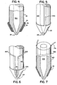
- Figure 4 is a partial longitudinal section of a modified bonding tool;
- Figure 5 is an elevation of a portion of another bonding tool;
- Figure 6 is an elevation of a portion of a further bonding tool;
- Figure 7 is an elevation, partially in section of a portion of another bonding tool showing permanently attached flexible power leads;
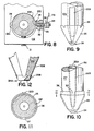
- Figure 8 is a sectional plan view of a modified tool holder showing alternative ways of attaching power leads;
- Figure 9 is an elevation of a portion of a modified bonding tool of the type shown in Figures 1 to 3;
- Figure 10 is an elevation of a portion of another modified bonding tool;
- Figure 11 is a section taken on the line 11-11 of Figure 10; and
- Figure 12 is a partial elevation of another shape of bonding tool.
- Refer now to Figures 1 to 3 showing a preferred embodiment of the present invention.
Bonding tool 10 is shown mounted in an ultrasonic transducer horn 11. The end of the transducer is split atslot 12 and is provided with acylindrical recess 13 adapted to receive the upper or mountingportion 14 ofbonding tool 10.Tool 10 is firmly inrecess 13 byclamp screw 15. -
Terminal mounting block 16 is supported on the bonding machine (not shown) adjacent to transducer horn 11. A pair ofleads 17 are connected at their upper ends to a source of electrical power (not shown). The upper ends of theleads 17 are preferably shaped to form a rigid fixed connection with the connector (not shown) in theterminal mounting block 16 which is made of insulating material. The vertical portions ofleads 17 extend down the face ofmounting block 16 on either side of acam screw 18 which is pivotably mounted inblock 16. When the insulatedcam screw 18 is rotated 180 degrees, the vertical portions ofleads 17 are forced apart which also forces the lowerhorizontal end portions 19 apart. In the preferred embodiment,leads 17 are made of resilient material and normally engage the sides of thebonding tool 10 but can be separated by thecam screw 18. Alternatively rigid leads may be spring-biased against the sides of the tool. It will be understood that thebonding tool 10 may be replaced more quickly and easily when theleads 17 are not engaging the sides of thetool 10. Threadedrecesses 21 are provided inmounting block 16 for attaching a cover plate (not shown) over theleads 17. - The bonding tool is made of dense alumina (over 99% density). The alumina shank or nib is commercially available and has a high dielectric strength. Alumina substrates which are used for miniaturized circuits or supports for integrated circuits, have lower density which provides greater porosity than the porosity of
bonding tool 10. - Contact
terminal pads 22 are deposited ontool 10 to provide elongated electrically conductive pads. Such pads may be deposited by evaporating, sputtering, erectrodepositing, etc. the conductive material. The preferred technique is an application of gold paste such as the pastes made by Engelhard Minerals and Chemical Company for line printing through metal mask or silk screening. Paths 125 pm (five mils) wide and up to 24.5 µm (one mil) thick may be applied with known techniques for applying paste. However, it was determined that such paste may also be applied by wooden spatulas or applied with thick ink applying tools. It was determined that fritiess gold conductive compositions provided better bonding characteristics when applied to high density alumina. Thepads 22 are set by heating and/or firing the applied paste. It should be noted that thefilm 23 or gold pads on thefilm 23 could also serve as the conductive pads. - A frusto-conical layer of electrically conductive-
resistive material 23 is then applied over the workingtip 24 ofbonding tool 10. While the material can be deposited by known sputtering, evaporating and electroplating techniques, an application of thick resistive composition paste such as A3001 resistor ink, made by Engelhard Minerals and Chemical Company, is preferred. Such thick pastes are prepared for application by silk screening and printing through slots and may be easily applied in thicknesses of up to one mil in a single operation. Greater thicknesses may be achieved by setting and/or firing a first layer and then applying a second layer to build up thefilm 23. - It was determined that thick films applied as paste compositions could be deposited on the tapered working
portion 24 to provide the conductive-resistive heating elements without further extension on the bonding tool. Such depositedfilms 23 have a normal working resistance in the range of 5 to 20 ohms between theconductive pads 22. It was further determined that maximum working temperatures could be obtained with about one-half watt of power. When one-half watt of power is generated by a 15 ohm heater film, the required applied voltage is only 2.74 volts. A 5 ohm heater film only requires 1.8 volts for operation. Stable temperatures in the range of 600°C have been achieved with the above described heating elements. - Since silicon-aluminium eutectics form at 540°C to 560°C, temperatures in excess of 600°C will tend to destroy most semiconductor devices. It is believed that temperatures in excess of 600°C are not presently required. However, should the state of the semiconductor art change to require higher temperatures, there are pastes which are capable of obtaining the high temperatures.
- Electrical current applied at
terminal block 16 is conducted vialeads 17 toterminal pads 22 ofbonding tool 10. The current is directed into the electrically conductive-resistive film 23 and splits into two parallel paths between theconductive pads 22. Theend portions 19 of the flexible leads, which leads haveinsulative sleeves 25 thereon, are best shown in Figure 2 in spring bias engagement withpads 22. When the ultrasonic tool holder 11 is active theend portions 19 tend to follow the vibratingtool 10, but do not tend to damp the energy being applied to thebonding tool 10. While an ultrasonic wirebonding tool holder 10 is shown in Figure 1, other types of tool holder may be employed. When other types of tool holder are employed often other shapes of working tips and working tools are employed. - A distinct advantage of the present heated bonding tool resides in its inherent ability to provide an indication of the temperature of the
tip 24 of the bonding tool. Resistive composition paste may be manufactured in a wide range of resistances which vary from 10 ohms per square to ten to the sixth (106) ohms per square. Ohms per square is herein defined as the resistivity p divided by the thickness t where the length I and the width w of the square area under test are equal. - When a conductive-resistive film having a high thermal coefficient of resistance is employed, small changes in working temperature result in measurable changes in resistance. Resistive pastes are available with high negative temperature coefficients and moderately high positive temperature coefficients. Automatic welding controllers are known which are capable of monitoring the resistance between the electrodes of a spot welder. Accordingly, the monitor presently employed does not require detailed explanation for description of this invention. A temperature monitor which monitors change of voltage preferably maintains constant current. A temperature monitor which monitors change of current preferably maintains constant voltage. In the present invention an A.C. or D.C. power source may be applied to the
conductive pads 22 ofbonding tool 10 and the resistance monitored by observing either voltage or current changes to indicate the actual temperature of the workingtip 24. It will be understood that initially the bonding tool is calibrated to determine the resistance versus temperature characteristic. - Figure 4 shows a modification of the bonding tool of Figure 3. The
resistive film 23 andterminal pads 22 remain as described with respect to Figure 3. An insulating layer orcoating 26 is applied over thefilm 23 to electrically isolate it. Thick film dielectric materials such as silicon dioxide or an equivalent are acceptable because only low voltages are employed on the bonding tools. A highlyreflective layer 27 is applied as an outer coating over the insulatinglayer 26. Even though the reflective layer may change its coefficient of emissivity slightly when operated at or near 600°C, it will retain most of its low emissivity coefficients so as to reduce radiated heat loss. A thin layer of aluminium oxide 100 nm (1000 A) or more in thickness will be sufficient to form areflective layer 27. In some embodiments of the present invention it may be desirable to add only theinsulative layer 26 to the bonding tool 10A, because at low operating temperatures the radiated heat loss is of little significance. - Figure 5 shows an alternative embodiment to the bonding tools of Figures 1 to 4. The base ceramic nib or capillary of bonding tool 10B is highly insulative. In certain environments it may be desirable to deposit both the conductive-
resistive film 23 and theterminal pads 22A as a single layer of the same material. Even though the voltage gradient across theterminal pads 22A will not be uniform, sufficient heat can be generated in the working tip of the bonding tool to merit the use of this simplified embodiment. - Figure 6 shows another modified bonding tool 10C. The conical shape electrically conductive-
resistive film 23A is provided with a slot orbare space 28. Conductive pads orpaths 22B extend underfilm 23A. The current path throughfilm 23A is now greater than 180° or circumference. The shortest path is at or near the point of the workingtip portion 24 as in previous embodiments. The resistance path being shorter near the tip causes greater current density near the working tip and in turn causes greater heating effect where it is desired and needed. It will be noted that the resistance monitor employed for temperature indications will require a different calibration from previously discussed embodiments. - Figure 7 shows another embodiment of a heated bonding tool 10D. The electrically conductive-
resistive film 23 is first deposited on the base capillary 10D and the terminal paths are applied on the outside of theresistive film 23. When thefilm 23 is fired at very high temperature, the gold paste need not be subject to the same high temperatures since it may be added in a secondary step. The electrical characteristics of the bonding tool shown in Figure 7 are the same as those of the tools of Figures 3 to 5. Figure 7 shows a further modification in that flexible leads 17A may be permanently attached to theconductive pads 22C. Parallel gap welding will attach theflexible copper conductors 17A to holdterminal pads 22C. When permanent leads 17A are attached to heating bonded tool 10D at the top of the tool, the tool may be inserted into a tool holder 11 from the top. Accordingly, the tool is made long enough to extend above the bonding tool holder 11. The sameflexible leads 17A may be attached at a point which is intermediate the ends of tool 10D, in which event it is preferred to terminatepads 22 at theleads 17A so they will not interfere with holder 11. - Figure 8 is a plan or top view of a heated bonding tool 10E similar to tool 10D which is mounted in a bonding tool holder 11 A. The
conductive pads 22C may extend completely through tool holder 11 A because slottedapertures 29 provide air insulation gaps betweenpads 22C and holder 11 A. The heated bonding tool 10E is first clamped in place byscrew 31 threaded through holder 11 A. It will be noted that tool holder 11 A is capable of holding any of theaforementioned tools 10 to 10E. In some environmental conditions it may be desirable to provide a pressure contact point on one or more sides of tool 10E. Accordingly, in insulatingsleeve 32 is fixed in tool amount 11 A. A conductive threadedscrew 33 is shown mounted in the threadedsleeve 32 and is adjusted to engage apad 22C on one side of bonding tool 1 OE. Thepad 22C on the other side of the bonding tool may be engaged by a similar conductive threadedscrew 33 or byterminal leads 17A described hereinbefore. Aflexible lead 17B is attached to screw 33 and preferably held in place bylock nuts 34 which are threaded onscrew 33. Other known spring urged devices may be employed in lieu of threadedscrew 33. - Figure 9 is a heated bonding tool similar to previously described tools.
Pad 22D is shown wider than the previously describedpads 22 to illustrate that the lower end which extends underfilm 23 may be tapered to produce a more uniform voltage gradient throughfilm 23. - It has been determined that the resistance of
film 23 can easily be duplicated under mass production conditions within fifteen percent (15%). Cutting back or trimming the top or even the bottom of theconical shape film 23 is a preferred method of adjusting the resistance. Notches such asnotch 35 are also a preferred way of adjusting the resistance of thefilm 23 after it is fired and hardened. - Figures 10 and 11 show a modified bonding tool 10F. The nib or capillary is made of conductive material such as tungsten, tungsten carbide or hard sintered powdered metals. An insulating
layer 36 is deposited over the conductive metal tool capillary 10F at the workingtip portion 24. The insulatinglayer 36 is provided with a bare space orslot 37 which exposes part of the workingtip portion 24. When theresistive film 23 is applied overlayer 36, thefilm 23 engages in electrical contact with theportion 24 exposed byslot 37. As best shown in Figure 10, the bonding tool capillary may be employed as a terminal pad which connects to film 23 atslot 37.Terminal pad 22D on the other side opposite theslot 37 may serve as a second terminal pad. It will now be understood that applying aninsulative layer 36 over any . metal conductive tool of any shape will render the conductive tool the same as a completely insulative ceramic tool. Further, theinsulative layer 36 can be placed on a conductive tool 10F of any shape to form complete insulative under- layment forpads 22 andfilm 23. - Figure 12 shows another modified bonding tool 10G. Bonding tools of the shape shown may be used for beam lead bonding or for inner lead and outer lead bonding of foil patterns. In the embodiment shown, the tool 10G is of a shape which is similar to those known in the prior art and have been employed with pulse energy. The
conductive terminal pads 22E are similar topads 22 of Figure 3. Film 23B is deposited on the sides of the tool 1 OG to complete the circuit therebetween. When the bonding tool base 10G is of a conductive material it may be desired to deposit an insulative under- layment under thepads 22E and film 23B. In operation, the current passing through the film 23B heats only the workingtip 24A. The film 23B may be made from high temperature compositions which easily withstand high temperatures. This will permit the base or body to be made of any type of material which was really not feasible with the prior art bonding tools of similar shape. - When making the aforementioned heated bonding tools it was discovered that numerous alternative steps could be employed to produce the structures shown. When carbide capillaries were used they were cleaned and dried just prior to the application of the composite thick film pastes. Spinning the capillary during application of the paste results in a more uniform coating. Drying the composite paste before firing the composite paste in a belt furnace produces more uniform layers and avoids the possibility of undesirable flow of the paste. The manner in which the pastes are thinned and/or applied is generally known and will not be described herein.
- Having explained preferred heated bonding tools, all of which employ a deposited paste conductive-resistive film it will be understood that other type of films and other methods of depositing the films and pads may be employed to produce the same novel heated bonding tools. The variations and modifications described hereinbefore are intended to illustrate the numerous ways in which the films may be connected to sources of power and the current conducted through a heating film. The features of the different figures were intended to provide features which could be interchanged. As an example, any of the basic film structures can be applied to either a conductive or a non-conductive wire bonding capillary, die bonding tool or multi-lead bonding tool. Further, any of the film heaters may be heated by pulse energy or continuous energy as the circumstances may require.
Claims (9)
Applications Claiming Priority (2)
| Application Number | Priority Date | Filing Date | Title |
|---|---|---|---|
| US05/894,344 US4315128A (en) | 1978-04-07 | 1978-04-07 | Electrically heated bonding tool for the manufacture of semiconductor devices |
| US894344 | 1978-04-07 |
Publications (3)
| Publication Number | Publication Date |
|---|---|
| EP0004787A2 EP0004787A2 (en) | 1979-10-17 |
| EP0004787A3 EP0004787A3 (en) | 1979-10-31 |
| EP0004787B1 true EP0004787B1 (en) | 1982-01-27 |
Family
ID=25402948
Family Applications (1)
| Application Number | Title | Priority Date | Filing Date |
|---|---|---|---|
| EP79300576A Expired EP0004787B1 (en) | 1978-04-07 | 1979-04-06 | Heated semiconductor bonding tool |
Country Status (4)
| Country | Link |
|---|---|
| US (1) | US4315128A (en) |
| EP (1) | EP0004787B1 (en) |
| JP (1) | JPS54139376A (en) |
| DE (1) | DE2961943D1 (en) |
Cited By (1)
| Publication number | Priority date | Publication date | Assignee | Title |
|---|---|---|---|---|
| DE102020114642A1 (en) | 2020-06-02 | 2021-12-02 | Hesse Gmbh | Bonding device and operating method therefor |
Families Citing this family (48)
| Publication number | Priority date | Publication date | Assignee | Title |
|---|---|---|---|---|
| JPS57139933A (en) * | 1981-02-23 | 1982-08-30 | Nec Corp | Assembling apparatus for semiconductor device |
| US4451968A (en) * | 1981-09-08 | 1984-06-05 | Texas Instruments Incorporated | Method and device for providing an ohmic contact of high resistance on a semiconductor at low temperatures |
| US4513190A (en) * | 1983-01-03 | 1985-04-23 | Small Precision Tools, Inc. | Protection of semiconductor wire bonding capillary from spark erosion |
| US4577797A (en) * | 1984-03-21 | 1986-03-25 | Rockwell International Corporation | Apparatus and method for making laminate structures |
| DE3641873C1 (en) * | 1986-12-08 | 1987-08-20 | Sachs Ersa Kg | Soldering tip |
| US4799615A (en) * | 1987-06-17 | 1989-01-24 | Davenport Michael L | Collet holder |
| JPH01201933A (en) * | 1988-02-08 | 1989-08-14 | Mitsubishi Electric Corp | Wire bonding and device therefor |
| JPH02101754A (en) * | 1988-10-11 | 1990-04-13 | Hitachi Ltd | Bonding process and bonding apparatus |
| DE69018220T2 (en) * | 1989-12-20 | 1995-07-27 | Sumitomo Electric Industries | Connecting tool. |
| ATE120678T1 (en) * | 1990-07-13 | 1995-04-15 | Siemens Ag | CERAMIC SOLDER IG. |
| US5142117A (en) * | 1990-11-20 | 1992-08-25 | Motorola, Inc. | Proximity heater for an ultrasonic bonding tool |
| US5186378A (en) * | 1991-09-30 | 1993-02-16 | Texas Instruments Incorporated | Method and apparatus for transducer heating in low temperature bonding |
| US5240166A (en) * | 1992-05-15 | 1993-08-31 | International Business Machines Corporation | Device for thermally enhanced ultrasonic bonding with localized heat pulses |
| US5290281A (en) * | 1992-06-15 | 1994-03-01 | Medicon Eg | Surgical system |
| US5816472A (en) * | 1994-01-28 | 1998-10-06 | Hewlett-Packard Company | Bonding tool for tape automated assembly |
| JPH07321153A (en) * | 1994-05-24 | 1995-12-08 | Matsushita Electric Ind Co Ltd | TCP mounting device |
| US5650081A (en) * | 1994-06-29 | 1997-07-22 | Zevatech, Inc. | Thermode solder blade with electric heater greater than four ohms |
| US5446819A (en) * | 1994-07-14 | 1995-08-29 | Itt Industries, Inc. | Termination tool and method for optical fibre cables |
| KR0186084B1 (en) * | 1995-09-02 | 1999-04-15 | 문정환 | Wedge tool with heating equipment |
| JP3455626B2 (en) * | 1996-03-13 | 2003-10-14 | 株式会社東芝 | Semiconductor device manufacturing method and manufacturing apparatus |
| AT405591B (en) * | 1997-10-03 | 1999-09-27 | Schaffler & Co | HEATING ELEMENT AND METHOD FOR THE PRODUCTION THEREOF |
| US6305923B1 (en) * | 1998-06-12 | 2001-10-23 | Husky Injection Molding Systems Ltd. | Molding system using film heaters and/or sensors |
| US20060261132A1 (en) * | 1999-02-25 | 2006-11-23 | Reiber Steven F | Low range bonding tool |
| US20080197172A1 (en) * | 1999-02-25 | 2008-08-21 | Reiber Steven F | Bonding Tool |
| US7124927B2 (en) * | 1999-02-25 | 2006-10-24 | Reiber Steven F | Flip chip bonding tool and ball placement capillary |
| US6354479B1 (en) * | 1999-02-25 | 2002-03-12 | Sjm Technologies | Dissipative ceramic bonding tip |
| US20070131661A1 (en) * | 1999-02-25 | 2007-06-14 | Reiber Steven F | Solder ball placement system |
| US20060071050A1 (en) * | 1999-02-25 | 2006-04-06 | Reiber Steven F | Multi-head tab bonding tool |
| US7389905B2 (en) | 1999-02-25 | 2008-06-24 | Reiber Steven F | Flip chip bonding tool tip |
| US6651864B2 (en) * | 1999-02-25 | 2003-11-25 | Steven Frederick Reiber | Dissipative ceramic bonding tool tip |
| US7032802B2 (en) * | 1999-02-25 | 2006-04-25 | Reiber Steven F | Bonding tool with resistance |
| US6497356B2 (en) | 2000-04-28 | 2002-12-24 | Kulicke & Soffa Investments, Inc. | Controlled attenuation capillary with planar surface |
| US6321969B1 (en) * | 2000-04-28 | 2001-11-27 | Kulicke & Soffa Investments | Efficient energy transfer capillary |
| US6523733B2 (en) | 2000-04-28 | 2003-02-25 | Kulicke & Soffa Investments Inc. | Controlled attenuation capillary |
| US6657165B1 (en) * | 2000-11-03 | 2003-12-02 | R. A. Jones & Co. Inc. | Sealing system for forming thermal seals and method of operation thereof |
| US6520399B1 (en) | 2001-09-14 | 2003-02-18 | Raytheon Company | Thermosonic bonding apparatus, tool, and method |
| US6873790B1 (en) * | 2003-10-20 | 2005-03-29 | Richard Cooper | Laminar air flow, low temperature air heaters using thick or thin film resistors |
| US7249702B2 (en) | 2003-12-04 | 2007-07-31 | Kulicke And Soffa Industries, Inc. | Multi-part capillary |
| US7427009B2 (en) * | 2004-06-24 | 2008-09-23 | Asm Technology Singapore Pte Ltd. | Capillary for wire bonding |
| US7322507B2 (en) * | 2005-01-17 | 2008-01-29 | Amkor Technology, Inc. | Transducer assembly, capillary and wire bonding method using the same |
| US7677432B2 (en) * | 2005-05-03 | 2010-03-16 | Texas Instruments Incorporated | Spot heat wirebonding |
| US20070085085A1 (en) * | 2005-08-08 | 2007-04-19 | Reiber Steven F | Dissipative pick and place tools for light wire and LED displays |
| JP2007335708A (en) * | 2006-06-16 | 2007-12-27 | Shinkawa Ltd | Wire bonder, wire bonding method and program |
| JP4941268B2 (en) * | 2007-12-17 | 2012-05-30 | 富士通株式会社 | Wire bonding method and wire bonding apparatus |
| FR3065330B1 (en) * | 2017-04-13 | 2019-05-03 | Tyco Electronics France Sas | TOOL FOR WELDING AN ELECTRICAL CONDUCTOR WITH A CONNECTING DEVICE |
| US10751822B2 (en) * | 2018-09-25 | 2020-08-25 | Ok International, Inc. | Smart soldering iron tip and method of authenticating same |
| US10751823B2 (en) * | 2018-09-25 | 2020-08-25 | Ok International, Inc. | Smart soldering iron tip and method of authenticating same |
| CN110385440B (en) * | 2019-07-29 | 2022-04-19 | 无锡精蓉创材料科技有限公司 | Production process of powder metallurgy deep cavity welding cleaver |
Family Cites Families (17)
| Publication number | Priority date | Publication date | Assignee | Title |
|---|---|---|---|---|
| US3007026A (en) * | 1948-10-21 | 1961-10-31 | George V Woodling | Electrical heating devices |
| US2859321A (en) * | 1955-07-11 | 1958-11-04 | Garaway Alexander | Electric resistance heater |
| US3136878A (en) * | 1960-06-23 | 1964-06-09 | Itt | Soldering iron |
| US3320401A (en) * | 1963-05-24 | 1967-05-16 | North American Aviation Inc | Diffusion bonder |
| US3358897A (en) * | 1964-03-31 | 1967-12-19 | Tempress Res Co | Electric lead wire bonding tools |
| US3384283A (en) * | 1964-10-16 | 1968-05-21 | Axion Corp | Vibratory wire bonding method and apparatus |
| US3271555A (en) * | 1965-03-29 | 1966-09-06 | Int Resistance Co | Handling and bonding apparatus |
| US3478191A (en) * | 1967-01-23 | 1969-11-11 | Sprague Electric Co | Thermal print head |
| US3569665A (en) * | 1969-03-28 | 1971-03-09 | Armstrong Cork Co | Fixed temperature, rapid response, high energy heating device |
| US3641304A (en) * | 1969-06-16 | 1972-02-08 | Kulicke & Soffa Ind Inc | Heated semiconductor bonding tool |
| US3617682A (en) * | 1969-06-23 | 1971-11-02 | Gen Electric | Semiconductor chip bonder |
| US3576969A (en) * | 1969-09-02 | 1971-05-04 | Ibm | Solder reflow device |
| US3650450A (en) * | 1969-11-24 | 1972-03-21 | Wells Electronics | Means for forming electrical joints between intermediate parts of an elongated conductor and selected conductive element on an electrical assembly |
| US3699588A (en) * | 1970-12-28 | 1972-10-17 | Honeywell Inc | Recorder for recording on heat-sensitive material |
| US3811030A (en) * | 1971-11-15 | 1974-05-14 | C Veach | Electrically heated stylus for transferring a printing medium |
| US3838240A (en) * | 1973-04-04 | 1974-09-24 | Rca Corp | Bonding tool and method of bonding therewith |
| US3920949A (en) * | 1974-03-13 | 1975-11-18 | Mallory & Co Inc P R | Beam leaded device welding machine |
-
1978
- 1978-04-07 US US05/894,344 patent/US4315128A/en not_active Expired - Lifetime
-
1979
- 1979-04-06 DE DE7979300576T patent/DE2961943D1/en not_active Expired
- 1979-04-06 EP EP79300576A patent/EP0004787B1/en not_active Expired
- 1979-04-06 JP JP4244079A patent/JPS54139376A/en active Granted
Cited By (3)
| Publication number | Priority date | Publication date | Assignee | Title |
|---|---|---|---|---|
| DE102020114642A1 (en) | 2020-06-02 | 2021-12-02 | Hesse Gmbh | Bonding device and operating method therefor |
| WO2021244703A2 (en) | 2020-06-02 | 2021-12-09 | Hesse Gmbh | Bonding apparatus and operating method therefor |
| WO2021244703A3 (en) * | 2020-06-02 | 2022-03-31 | Hesse Gmbh | Wire bonding apparatus, and operating method therefor |
Also Published As
| Publication number | Publication date |
|---|---|
| JPS5758059B2 (en) | 1982-12-08 |
| DE2961943D1 (en) | 1982-03-11 |
| EP0004787A2 (en) | 1979-10-17 |
| US4315128A (en) | 1982-02-09 |
| EP0004787A3 (en) | 1979-10-31 |
| JPS54139376A (en) | 1979-10-29 |
Similar Documents
| Publication | Publication Date | Title |
|---|---|---|
| US4315128A (en) | Electrically heated bonding tool for the manufacture of semiconductor devices | |
| JP2726130B2 (en) | Fuse for small ampere comprising metal organic material film and method of manufacturing the same | |
| US5999085A (en) | Surface mounted four terminal resistor | |
| US4788523A (en) | Viad chip resistor | |
| JPH0750128A (en) | Microminiature fuse | |
| GB2241392A (en) | Microfuse. | |
| CA1040746A (en) | Thin film resistance temperature detector | |
| KR100231080B1 (en) | Method for active metallization of mini igniters by raw sand screening | |
| KR100615443B1 (en) | Ceramic heater | |
| JP2002057009A (en) | Resistor and method of manufacturing the same | |
| US4401065A (en) | Glow plugs for use in diesel engines | |
| US6530776B1 (en) | Method and apparatus of connection to an electrical film device | |
| EP0812665B1 (en) | Hot cutting blade | |
| US5343021A (en) | Heater mounted on a substrate having a hole penetrating through the substrate | |
| US4853671A (en) | Electric laminar resistor and method of making same | |
| US4920635A (en) | A method of manufacturing a thermo-sensitive resistor | |
| US3071749A (en) | Adjustable resistors and method of making the same | |
| JP3872256B2 (en) | Wafer heating device | |
| JPH06106758A (en) | Thermal head | |
| KR100840796B1 (en) | Terminal for Ceramic Heating Element | |
| US5048180A (en) | Method of bonding a semiconductor device with a substrate | |
| US5794327A (en) | Method for making copper electrical connections | |
| JP3199575B2 (en) | heater | |
| RU189715U1 (en) | Power Thin Film Resistor | |
| JPH04231173A (en) | Soldering tool for ceramic |
Legal Events
| Date | Code | Title | Description |
|---|---|---|---|
| PUAI | Public reference made under article 153(3) epc to a published international application that has entered the european phase |
Free format text: ORIGINAL CODE: 0009012 |
|
| PUAL | Search report despatched |
Free format text: ORIGINAL CODE: 0009013 |
|
| AK | Designated contracting states |
Designated state(s): CH DE FR GB |
|
| AK | Designated contracting states |
Designated state(s): CH DE FR GB |
|
| 17P | Request for examination filed | ||
| GRAA | (expected) grant |
Free format text: ORIGINAL CODE: 0009210 |
|
| AK | Designated contracting states |
Designated state(s): CH DE FR GB |
|
| REF | Corresponds to: |
Ref document number: 2961943 Country of ref document: DE Date of ref document: 19820311 |
|
| PGFP | Annual fee paid to national office [announced via postgrant information from national office to epo] |
Ref country code: FR Payment date: 19830330 Year of fee payment: 5 |
|
| PGFP | Annual fee paid to national office [announced via postgrant information from national office to epo] |
Ref country code: CH Payment date: 19830331 Year of fee payment: 5 |
|
| PGFP | Annual fee paid to national office [announced via postgrant information from national office to epo] |
Ref country code: DE Payment date: 19830630 Year of fee payment: 5 |
|
| PG25 | Lapsed in a contracting state [announced via postgrant information from national office to epo] |
Ref country code: CH Effective date: 19840430 |
|
| GBPC | Gb: european patent ceased through non-payment of renewal fee | ||
| PG25 | Lapsed in a contracting state [announced via postgrant information from national office to epo] |
Ref country code: FR Free format text: LAPSE BECAUSE OF NON-PAYMENT OF DUE FEES Effective date: 19841228 |
|
| REG | Reference to a national code |
Ref country code: CH Ref legal event code: PL |
|
| PG25 | Lapsed in a contracting state [announced via postgrant information from national office to epo] |
Ref country code: DE Effective date: 19850101 |
|
| REG | Reference to a national code |
Ref country code: FR Ref legal event code: ST |
|
| PG25 | Lapsed in a contracting state [announced via postgrant information from national office to epo] |
Ref country code: GB Effective date: 19881117 |
|
| PLBE | No opposition filed within time limit |
Free format text: ORIGINAL CODE: 0009261 |
|
| STAA | Information on the status of an ep patent application or granted ep patent |
Free format text: STATUS: NO OPPOSITION FILED WITHIN TIME LIMIT |