EP0004757A1 - Système de mesure capacitif sans contact - Google Patents
Système de mesure capacitif sans contact Download PDFInfo
- Publication number
- EP0004757A1 EP0004757A1 EP79300529A EP79300529A EP0004757A1 EP 0004757 A1 EP0004757 A1 EP 0004757A1 EP 79300529 A EP79300529 A EP 79300529A EP 79300529 A EP79300529 A EP 79300529A EP 0004757 A1 EP0004757 A1 EP 0004757A1
- Authority
- EP
- European Patent Office
- Prior art keywords
- probe
- workpiece
- probes
- capacitance
- output
- Prior art date
- Legal status (The legal status is an assumption and is not a legal conclusion. Google has not performed a legal analysis and makes no representation as to the accuracy of the status listed.)
- Withdrawn
Links
- 239000000523 sample Substances 0.000 claims abstract description 129
- 230000000712 assembly Effects 0.000 claims abstract description 25
- 238000000429 assembly Methods 0.000 claims abstract description 25
- 238000012545 processing Methods 0.000 claims abstract description 21
- 238000005070 sampling Methods 0.000 claims abstract description 15
- 230000003534 oscillatory effect Effects 0.000 claims abstract description 6
- 238000012546 transfer Methods 0.000 claims abstract description 6
- 238000011156 evaluation Methods 0.000 claims abstract description 5
- 230000001419 dependent effect Effects 0.000 claims abstract description 4
- 230000006870 function Effects 0.000 claims description 12
- 230000015654 memory Effects 0.000 claims description 9
- 230000003321 amplification Effects 0.000 claims description 5
- 238000003199 nucleic acid amplification method Methods 0.000 claims description 5
- 238000004519 manufacturing process Methods 0.000 claims description 2
- 230000004044 response Effects 0.000 claims description 2
- 239000003990 capacitor Substances 0.000 abstract description 17
- 239000000872 buffer Substances 0.000 description 6
- 230000008901 benefit Effects 0.000 description 5
- 230000000694 effects Effects 0.000 description 5
- 238000005259 measurement Methods 0.000 description 4
- 230000007423 decrease Effects 0.000 description 3
- 238000010586 diagram Methods 0.000 description 3
- 230000008859 change Effects 0.000 description 2
- 238000000034 method Methods 0.000 description 2
- 230000003466 anti-cipated effect Effects 0.000 description 1
- 238000013459 approach Methods 0.000 description 1
- 238000010276 construction Methods 0.000 description 1
- 238000013461 design Methods 0.000 description 1
- 230000008030 elimination Effects 0.000 description 1
- 238000003379 elimination reaction Methods 0.000 description 1
- 239000011888 foil Substances 0.000 description 1
- 238000007373 indentation Methods 0.000 description 1
- 230000000704 physical effect Effects 0.000 description 1
- 238000003908 quality control method Methods 0.000 description 1
- 239000010453 quartz Substances 0.000 description 1
- 230000035945 sensitivity Effects 0.000 description 1
- VYPSYNLAJGMNEJ-UHFFFAOYSA-N silicon dioxide Inorganic materials O=[Si]=O VYPSYNLAJGMNEJ-UHFFFAOYSA-N 0.000 description 1
- 238000012360 testing method Methods 0.000 description 1
- 238000004804 winding Methods 0.000 description 1
Images
Classifications
-
- G—PHYSICS
- G01—MEASURING; TESTING
- G01B—MEASURING LENGTH, THICKNESS OR SIMILAR LINEAR DIMENSIONS; MEASURING ANGLES; MEASURING AREAS; MEASURING IRREGULARITIES OF SURFACES OR CONTOURS
- G01B7/00—Measuring arrangements characterised by the use of electric or magnetic techniques
- G01B7/28—Measuring arrangements characterised by the use of electric or magnetic techniques for measuring contours or curvatures
- G01B7/287—Measuring arrangements characterised by the use of electric or magnetic techniques for measuring contours or curvatures using a plurality of fixed, simultaneously operating transducers
-
- G—PHYSICS
- G01—MEASURING; TESTING
- G01B—MEASURING LENGTH, THICKNESS OR SIMILAR LINEAR DIMENSIONS; MEASURING ANGLES; MEASURING AREAS; MEASURING IRREGULARITIES OF SURFACES OR CONTOURS
- G01B7/00—Measuring arrangements characterised by the use of electric or magnetic techniques
- G01B7/02—Measuring arrangements characterised by the use of electric or magnetic techniques for measuring length, width or thickness
- G01B7/023—Measuring arrangements characterised by the use of electric or magnetic techniques for measuring length, width or thickness for measuring distance between sensor and object
Definitions
- the invention relates to a capacitive non-contact gauging system which is particularly, though not exclusively, useful for measuring the surface characteristics of a workpiece.
- Capacitive non-contact gauging systems utilize a noncontacting probe which forms with a workpiece, in effect, a variable capacitor whose capacitance varies with the spacing between the workpiece and the probe.
- Various schemes have been used to measure this capacitance and produce an electric signal which is indicative of the probe to workpiece distance. Examples of one method of doing this are shown in U.S. Patent Nos. 3,716,782 and 3,775,679 and use the variable capacitance to modify the frequency of an oscillator, which change in frequency is used Lo produce the output distance indicative signal.
- a capacitor of known capacitance and the probe to workpiece capacitance act as a voltage divider and the ratio of voltage across both capacitances varies as the variable capacitance varies, the output from the voltage divider being processed and normally transformed into an indication of the distance between the probe and the workpiece.
- the present invention provides a capacitive non-contact gauging system comprising a plurality of probes adapted each to be positioned proximate a workpiece so as to constitute with the workpiece a capacitance the magnitude whereof is a function of the probe to workpiece distance, a plurality of output circuits each individually associated with a respective one of said probes for deriving therefrom in response to the application of an electrical signal thereto a signal representative of the respective probe to workpiece capacitance according to known characteristics of the respective output circuit, means for storing information pertaining to the said known characteristics of each of said output circuits, and pro- ; cessing means for deriving for each of said plurality of probes from the said signal derived by the.respective output circuit associated therewith a probe to workpiece distance evaluation taking account in each case of the stored information pertaining to the said known characteristics of respective output circuit.
- an amplitude sensitive system that is to say a system of the type wherein the capacitance established between a workpiece and a probe spaced from the workpiece, which capacitance is a function of the probe to workpiece spacing, is compared with a known capacitance coupled to the probe by applying an oscillatory electrical signal between the known capacitance and the workpiece and sensing the amplitude of the signal developed at the probe, which amplitude is dependent upon the relationship of the probe to workpiece capacitance to the known capacitance and represents a measure of the probe to workpiece distance.
- the invention provides a system comprising a plurality of probes each having a corresponding known capacitance coupled thereto, an oscillator feeding an oscillatory signal to each of said plurality of probes, a plurality of output circuits each coupled to a respective one of said probes to receive therefrom the signal developed thereat, which signal has an amplitude representative of the probe to workpiece distance at the respective probe, means for storing information pertaining to known transfer characteristics of each of said output circuits, and processing means coupled to said output circuits and to said storage means for deriving for each of said plurality of probes from the said signal developed thereat a probe to workpiece distance evaluation taking account in each case of the stored transfer characteristic information in respect of the respective output circuit.
- the invention provides a capacitive non-contact gauging apparatus including a plurality of head assemblies each head assembly containing a plurality of probe assemblies; a plurality of multiplexer means one connected with each of said head assemblies for sampling each of the probes in the head assembly to which it is connected; central multiplexer means connected to each of said multiplexer means for sampling the outputs of each of said multiplexer means; and a central processing unit connected to the output of said central multiplexer means for producing output signals which are a function of the spacing between each of the probes in each of said head assemblies and a workpiece.
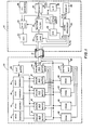
- the gauging system shown in Figure 1 has two segments, the remote or measuring unit 10, and the control or central unit 12.
- Measuring unit 10 which holds the probe elements along with related circuitry is normally positioned to come into close proximity to the workpiece to be tested.
- the central unit 12 contains the common signal processing equipment and, optionally, the output display unit 48.
- the measuring unit and the control unit are connected by a section of cable 14.
- the measuring unit consists of a plurality of head assemblies 16.
- the exact structure of the head assemblies will be shown and described in more detail in connection with Figure 2. Any number of head assemblies may be used, however for digital processing equipment 16 head assemblies has been found to be a convenient number.
- Each of the head assemblies contains a multiplicity of probes, a capacitive voltage divider for each probe, and an amplifier which buffers each voltage divider and decreases the output impedance.
- the output of each head assembly is connected to an analog multiplexer and buffer circuit 18.
- Each of the analog multiplexer and buffers 18 have an output connected to analog multiplexer and buffer 20.
- the analog multiplexers 18 sequentially sample each of the multiplicity of probes within the head assembly to which they are connected.
- the analog multiplexer 20 sequentially samples each of the multiplexers 18. In this manner, a sequential sampling of all the probes is accomplished.
- the output of analog multiplexer 20 is a series of signals each indicative of the capacitance between one of the probes and the workpiece, which
- the system is very sensitive to capacitance and slight variations in the tolerances of the components which make up the circuits. This sensitivity is especially noticeable in the amplifiers for each of the probes. With precision manufacturing and calibration the individual amplifiers could be made to have the same circuit characteristics. However, such precision is monetarily and time wise a consuming operation.
- the present invention overcomes the need for this with a series of programmable read only memories (PROM's) 22.
- PROM's programmable read only memories
- Each of the PROM's 22 has an output connected to a digital multiplexer 24.
- the outputs of the multiplexers will then be a series of signals representing the output voltage from each of the head assembly amplifiers on line 28 and the corresponding circuit constants for that amplifier i on line 30.
- control unit 12 the analog voltage indicative of the relative capacitance or distance between the probes and the workpiece comes into control unit 12 through cable 14 on line 28.
- the signal first goes to the auto zero control circuit 32.
- This ; circuit does not operate on the analog voltage, but rather is an automatic calibration circuit which, between samplings, is able to cut off the input on line 28 and ground the line going into the signal processing circuitry.
- the microprocessor 34 sends a command to the auto zero circuit to ground the input of the signal processing equipment, it correspondingly adjusts the output signal to zero. In this manner it automatically calibrates the circuitry in the control circuit system 12.
- oscillator 52 Also in the control unit 12 is oscillator 52.
- the oscillator produces a high frequency oscillating voltage with a very rigidly controlled amplitude. By way of example, a frequency of 200 kilohertz and a 12 volts peak to peak voltage have been found to be satisfactory.
- the oscillator output signal is applied through oscillator buffer 54 to the input of each of the probe amplifiers in each of the head assemblies 16.
- the oscillator signal is connected to each of the analog multiplexers/buffers 18. This enables the oscillator voltage to be sampled periodically by each of the analog multiplexers for automatic recalibration. For example, by sampling the oscillator voltage once with each scanning of the fifteen probes within one of the heads, the oscillator can be automatically recalibrated.
- To calibrate the oscillator 52 there is an auto gain circuit 56.
- a control line from the microprocessor 34 also causes the auto gain circuit 56 to compare the output voltage of rectifier filter 36 with a d.c. reference voltage 58. If the voltages do not match, auto gain circuit 56 adjusts the rigidly controlled oscillator voltage accordingly.
- the analog voltage signals on line 28 are passed through circuit 32 to the i rectifier and filter circuit 36.
- the signal coming in to the rectifier filter circuit 36 will be in the form of an oscillating voltage signal whose amplitude is indicative of the probe to workpiece spacing.
- Circuit 36 first rectifies this oscillating signal with a full wave rectifier and then filters the rectified signal to produce a steady state or DC analog voltage which is proportional in amplitude to the probe to workpiece spacing.
- This analog signal, V goes to a divider circuit 40 and to a sub- ; traction circuit 42.
- the microprocessor For each voltage V o corresponding to one of the probes, the microprocessor reads on line 30 the constants K 1 and K 2 corresponding to the same probe and feeds the constant K 2 to a digital to analog converter 44.
- the output digital to analog converter 44 forms a second input to subtraction circuit 42.
- the output signal of subtraction circuit 42, K 2 -V o , and the output from rectifier filter circuit 36, V are both fed to divider circuit 40.
- Circuit 40 divides the output of the rectifier filter circuit by the output of the subtraction circuit.
- the output of the divider is then fed to an analog to digital converter 46, which transforms the ratio produced by divider 40 into a digital signal and feeds it to the microprocessor 34.
- Microprocessor 34 multiplies this signal by the constant K 1 to get a final signal which may be expressed as As will be explained in the following, this equation represents the distance between the probe and the workpiece.
- This value is normally put into temporary storage in the micro-processor. From the temporary storage it is read out to a display device such as that shown in U.S. patent application Serial No. 855,128 or 855,522, to other suitable display devices, or to a memory device to be recorded for later recall.
- the microprocessor can compare each distance value with a series of preselected values. For example, a standardized workpicce, which is exactly to tolerances, could be placed adjacent the probe assembly and the distance values calculated and stored in microprocessor 34 or the microprocessor could be programmed with the ideal values.
- the microprocessor may be programmed to subtract the distance values obtained for each subsequent workplace from the values determined for the standard and to display the deviation from the standard.
- the display may be a straight line when the workpiece is perfect with deflections above the line indicating a bulge and deflections below the line indicating an indentation.
- an accept or reject signal can be produced, which signal will cause automated workpiece handling equipment to place the work- piece in either an acceptable or unacceptable pile.
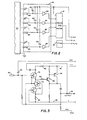
- FIG. 2 shows a close up of one of the head assemblies 16 and related structure.
- each head assembly there are a plurality of probe elements 60.
- the probe assembly and workpiece 62 are brought into close proximity.
- the probe and the workpiece will, in effect, be the plates of a variable capacitor. As a probe 60 and workpiece 62 come closer together with capacitance increases, and as they move further apart the capacitance decreases, producing in effect a variable capacitance.
- Each of the probe workpiece capacitances along with one of the capacitors 64 form a capacitive voltage divider for the oscillating voltage from the oscillator 52. Between each of these two capacitive elements is connected the input to one of amplifiers 66. It can be seen that the input to each amplifier will be a higher voltage when the effective capacitance between 60 and 62 decreases and a lower amplitude voltage when the effective capacitance between 60 and 62 increases. The output voltage from each amplifier 66 will then be a function of the capacitance between its associated probe 60 and workpiece 62 which is to say, a function of the distance between one of the probes 60 and workpiece 62.
- capacitor 64 is temperature stable. Because capacitor 64 is used as a reference capacitance, the voltage divider is in effect, finding the ratio of the two capacitances. Thus, the capacitance of capacitor 64 should be readily determinable and should not change during the operation from such causes as temperature fluctuations. A quartz capacitor has been found suitable for this purpose. The capacitance of capacitor 64 is normally comparable with the mean probe workpiece capacitance which is a function of probe size, mean probe workpiece spacing, etc., a 0.35 pf capacitance has been found to be effective.
- a stable amplifier suitable for use as amplifier 66 is shown in Figure 3. From the midpoint of the capacitive divider formed by capacitor 64 and the probe workpiece capacitance the amplifier input is connected to the gate of FET 70.
- a constant current source which in the preferred embodiment is composed of a pair of FET's 72 and 74.
- a line 76 connected to a positive biasing voltage, e.g., +15 volts, and a line 78 connected to a negative biasing voltage, e.g., -15 volts, along with biasing resistors 80 and 82.
- This first stage of amplification then has a very low input capacitance and very high impedance. With bootstrapping, careful circuit construction and guarding, the input capacitance may be kept on the order of .01 pf.
- the output of the first stage at resistor 84 presents a voltage which is a function of the probe to workpiece spacing.
- the second stage of amplification is performed by a pair of transistors 86 and 88. These two transistors provide a two stage amplification of the signal at resistor 84 and provide an output on line 90 which again is a function of the spacing between the probe and workpiece.
- transistors which have been found compatible in the above system include 2N4416 for FET's 70 and 72, 2N4338 for FET 74, 2N3904 for transistor 86 and 2N3906 for transistor 88.
- the diameter of the probe is determined by looking to the spacing between sampling points desired and by looking to the anticipated mean distance between the probes and the workpiece.
- the probe should be large enough in diameter compared with the distance between the probe and workpiece that capacitive edge effects are minimized, i.e., the smaller the probe diameter, the closer the workpiece should be to the probe.
- a larger diameter probe is desirable.
- the larger the probe diameter the greater the spacing between sampling positions. It can be seen that a trade-off must be reached in the area of probe diameter.
- Probe diameters of 0.1 inch, .25 inch and .50 inch have been found to be successful.
- An 0.1 inch diameter probe for example, has been found successful in measuring a workpiece to probe spacing which varies from 5 to 25 mils to an accuracy of within 10 microinches (.010 mils).
- capacitors 64 and the capacitance between each probe 60 and workpiece 62 work as a voltage divider.
- the voltage input into an amplifier 66 will be to the voltage of the oscillator as the capacitance of the stable reference capacitor.64 is to the total capacitance of capacitor 64 plus the probe workpiece capacitance.
- V o is the voltage out of amplifier 6b
- A is the amplification factor of the amplifier 6 6
- V osc is the voltage amplitude of the oscillator output
- C in is the capacitance of capacitor 64
- C g is the internal capacitance of the amplifier 66
- C p is the capacitance between probe 60 and workpiece 62.
- the capacitance between 60 and 62 can also be expressed as:
- the system aforedescribed presents many improvements over other amplitude sensitive systems and frequency modulation systems.
- One of the advantages is in the elimination of parallel parts.
- Many of the prior systems required an oscillator and signal processing circuitry for each probe.
- the system described by contrast, has a single oscillator and a single signal processing circuit for a large multiplicity of probes.
- An additional advantage of the system is its temperature stability.
- the changes in capacitance between the probes and the workpieces are generally very small which makes capacitive measuring systems very susceptible to error from temperature changes and stray capacitance. Small changes in temperature have been found to cause large variations in many systems.
- the very low input capacitance and high impedance unity gain amplifier improves temperature stability.
- the amplifier disclosed has been found to be accurate to 0.1% over a temperature range of 35 to 150°F.
- the disclosed system because of its temperature stability and other superior design characteristics, is able to measure very small changes in distance. Distances! of a few millionths of an inch can be detected. This great precision is required when measuring many surface characteristics such as straightness or conformance to a contour.
- the present gauging machine finds ready use for determining the flatness of machine molded, stamped, cast or fabricated parts, the straightness of cylinder walls or holes, and the conformance to specified contours of such complex parts as step shafts, air foils, and turbine blades.
- a further advantage of the present invention is its rapid measuring ability. Although the speed will vary with the number of probes used, it has been found that with 240 probes the present invention can usually produce an indication of the conformance of a workpiece at 240 positions within 5 seconds. This rapidity increases the precision of measurement instruments because the surface contour of the workpiece can be sampled at such a large number of points. Further, this rapidity enables testing equipment to sample large numbers of workpieces in a relatively short amount of operating time.
- the present system has a further advantage in that the large number of probes can be arranged in a linear array or in a grid array or along a winding contour or in almost any other array.
- a linear array produces the ; most easily understood two dimensional display of surface contour. Because a linear array can measure 200 or more points along a single line of contact of the workpiece, the system can produce a very detailed two dimensional, cross section-like view of the surface along the line of closest proximity between the workpiece and the line of probes. The workpiece may be shifted or rotated, to view other line segments along along its surface.
Landscapes
- Physics & Mathematics (AREA)
- General Physics & Mathematics (AREA)
- Measurement Of Length, Angles, Or The Like Using Electric Or Magnetic Means (AREA)
Applications Claiming Priority (2)
| Application Number | Priority Date | Filing Date | Title |
|---|---|---|---|
| US891957 | 1978-03-31 | ||
| US05/891,957 US4190797A (en) | 1978-03-31 | 1978-03-31 | Capacitive gauging system utilizing a low internal capacitance, high impedance amplifier means |
Publications (1)
| Publication Number | Publication Date |
|---|---|
| EP0004757A1 true EP0004757A1 (fr) | 1979-10-17 |
Family
ID=25399115
Family Applications (1)
| Application Number | Title | Priority Date | Filing Date |
|---|---|---|---|
| EP79300529A Withdrawn EP0004757A1 (fr) | 1978-03-31 | 1979-03-30 | Système de mesure capacitif sans contact |
Country Status (8)
| Country | Link |
|---|---|
| US (1) | US4190797A (fr) |
| EP (1) | EP0004757A1 (fr) |
| JP (1) | JPS54133368A (fr) |
| CA (1) | CA1138113A (fr) |
| DE (1) | DE2952825A1 (fr) |
| FR (1) | FR2454084A1 (fr) |
| GB (1) | GB2041540B (fr) |
| IT (1) | IT1148230B (fr) |
Cited By (18)
| Publication number | Priority date | Publication date | Assignee | Title |
|---|---|---|---|---|
| WO1982000195A1 (fr) * | 1980-07-07 | 1982-01-21 | Ab Viak | Dispositif de mesure des dimensions d'une lingotiere |
| JPS5870103A (ja) * | 1981-09-30 | 1983-04-26 | ゼネラル・エレクトリック・カンパニイ | 物体表面層の電気的性質の変化を測定する方法および走査容量顕微鏡 |
| FR2554223A1 (fr) * | 1983-10-28 | 1985-05-03 | Control Data Corp | Jauge de hauteur a capacite et procede et appareil d'etalonnage de cette jauge |
| WO1985004005A1 (fr) * | 1984-03-02 | 1985-09-12 | Hanson Research Limited | Mesures a l'aide de transducteurs electriques |
| DE3617373A1 (de) * | 1986-05-23 | 1987-11-26 | Mtu Muenchen Gmbh | Kapazitives messsystem |
| GB2194640A (en) * | 1986-08-29 | 1988-03-09 | Analytical Instr Ltd | Hermetically sealed package tester |
| EP0277421A1 (fr) * | 1986-12-05 | 1988-08-10 | The University Of Western Australia | Dispositif de capteurs de la capacitance |
| EP0281610A1 (fr) * | 1986-09-03 | 1988-09-14 | Extrude Hone Corporation | Reseau de capteurs a condensateurs pour la detection tactile et de proximite et leurs procedes d'utilisation |
| EP0303563A2 (fr) * | 1987-06-11 | 1989-02-15 | C.A. Weidmüller GmbH & Co. | Capteur avec dispositif de compensation |
| EP0425823A1 (fr) * | 1989-09-29 | 1991-05-08 | Antivision Systems Corp. | Système électrostatique pour former des images |
| WO1992006350A1 (fr) * | 1990-10-03 | 1992-04-16 | Renishaw Plc | Sondes a capacitance |
| WO1992008947A1 (fr) * | 1990-11-16 | 1992-05-29 | Moonstone Designs Limited | Dispositif permettant de determiner la presence et/ou les caracteristiques d'un objet ou d'une substance |
| EP0544022A1 (fr) * | 1990-10-09 | 1993-06-02 | Agr International, Inc. | Appareil et procédé d'inspection de l'épaisseur des parois d'un récipient en verre |
| EP0556682A1 (fr) * | 1992-02-10 | 1993-08-25 | SYEL di FRANCHI A.- MARTOLINI A. & C. s.n.c. | Appareil en forme de barre ayant des capteurs pour déterminer la forme et la proximité des objets de matériaux différents |
| FR2690244A1 (fr) * | 1992-01-10 | 1993-10-22 | Leteurtre Jean | Procédé et/ou dispositif de mise en Óoeuvre du procédé de mesure capacitive susceptible d'effectuer des mesures dimensionnelles sans contact et de très haute précision en milieu industriel. |
| US5272443A (en) * | 1992-04-22 | 1993-12-21 | Aluminum Company Of America | Chatter and profile measuring using capacitor sensors |
| FR2705145A1 (fr) * | 1993-05-10 | 1994-11-18 | Exa Ingenierie | Dispositif de mesure de rectitude. |
| EP0984329A2 (fr) * | 1998-09-04 | 2000-03-08 | Canon Kabushiki Kaisha | Appareil pour la détection de la position ayant une pluralité de sections de détection et appareil d'exposition |
Families Citing this family (22)
| Publication number | Priority date | Publication date | Assignee | Title |
|---|---|---|---|---|
| US4350040A (en) * | 1980-06-26 | 1982-09-21 | The United States Of America As Represented By The United States Department Of Energy | Capacitance-level/density monitor for fluidized-bed combustor |
| USRE32457E (en) * | 1981-09-30 | 1987-07-07 | Rca Corporation | Scanning capacitance microscope |
| US4476430A (en) * | 1982-04-05 | 1984-10-09 | Wright Wade S | Non-contact sensor for determining moving flat steel strip shape profile |
| US4646009A (en) * | 1982-05-18 | 1987-02-24 | Ade Corporation | Contacts for conductivity-type sensors |
| CA1191261A (fr) * | 1983-12-14 | 1985-07-30 | Francois Lalonde | Appareil de mesure dynamique et sans contact de faibles distances |
| US4860229A (en) * | 1984-01-20 | 1989-08-22 | Ade Corporation | Wafer flatness station |
| US4935700A (en) * | 1985-08-09 | 1990-06-19 | Washington Research Foundation | Fringe field capacitive sensor for measuring the size of an opening |
| US4820971A (en) * | 1986-05-29 | 1989-04-11 | Ko Wen Hsiung | Precision impedance variation measurement circuit |
| GB8718606D0 (en) * | 1987-08-06 | 1987-09-09 | Hiltcroft Packaging Systems Lt | Monitoring apparatus |
| CA1332183C (fr) * | 1989-06-23 | 1994-09-27 | Richard W. Henderson | Reseau de sondage capacitif |
| DE4022563A1 (de) * | 1990-04-11 | 1991-10-17 | Flachglas Ag | Verfahren zur kontaktlosen messung des elektrischen widerstands eines untersuchungsmaterials |
| GB2279756B (en) * | 1990-11-16 | 1995-06-07 | Moonstone Technology Ltd | Device for determining the presence and/or characteristics of an object or a substance |
| US5214388A (en) * | 1992-05-28 | 1993-05-25 | The United States Of America As Represented By The Administrator Of The National Aeronautics And Space Administration | Phase discriminating capacitive array sensor system |
| US5505072A (en) * | 1994-11-15 | 1996-04-09 | Tekscan, Inc. | Scanning circuit for pressure responsive array |
| US6144892A (en) * | 1996-02-08 | 2000-11-07 | Royal Master Grinders, Inc. | Gauging system |
| US5786698A (en) * | 1996-03-07 | 1998-07-28 | Ade Corporation | Transducer Bootstrapping apparatus |
| US6227938B1 (en) | 1998-09-08 | 2001-05-08 | Royal Masters Grinders, Inc. | Guidewire position locator |
| US6476621B1 (en) | 2001-06-29 | 2002-11-05 | Ade Corporation | Self-bootstrapping transducer interface |
| US6964205B2 (en) * | 2003-12-30 | 2005-11-15 | Tekscan Incorporated | Sensor with plurality of sensor elements arranged with respect to a substrate |
| US6993954B1 (en) * | 2004-07-27 | 2006-02-07 | Tekscan, Incorporated | Sensor equilibration and calibration system and method |
| JP6017096B1 (ja) * | 2015-10-30 | 2016-10-26 | 三菱電機株式会社 | ワイヤ放電加工機、ワイヤ放電加工機の制御装置の制御方法及び位置決め方法 |
| USD800983S1 (en) * | 2016-08-26 | 2017-10-24 | Shelita Lee | Lottery ticket scratcher |
Citations (3)
| Publication number | Priority date | Publication date | Assignee | Title |
|---|---|---|---|---|
| DE2158320A1 (de) * | 1971-11-24 | 1973-05-30 | Ferdy Dr Mayer | Vorrichtung zur beruehrungsfreien relativen abstandsmessung |
| DE2550427A1 (de) * | 1974-11-11 | 1976-05-13 | Kaman Sciences Corp | Abstandsmess-system und verfahren zum messen von abstaenden |
| DE1914045B2 (de) * | 1969-03-19 | 1976-07-08 | Messer Griesheim Gmbh, 6000 Frankfurt | Vorrichtung zur kapazitiven abstandermittlung |
Family Cites Families (11)
| Publication number | Priority date | Publication date | Assignee | Title |
|---|---|---|---|---|
| US3753373A (en) * | 1965-10-22 | 1973-08-21 | Bissett Berman Corp | Transducer system |
| US3805150A (en) * | 1970-08-17 | 1974-04-16 | Ade Corp | Environment immune high precision capacitive gauging system |
| CH538114A (de) * | 1971-05-06 | 1973-06-15 | Bauer Messinstrumente Ag | Vorrichtung zur Digitalen, kapazitiven Messung der örtlichen Lage von Trennschichten zwischen mindestens zwei aneinandergrenzenden Medien |
| US3716782A (en) * | 1971-06-03 | 1973-02-13 | J Henry | Capacitance gage for measuring small distances |
| US3775679A (en) * | 1971-12-09 | 1973-11-27 | Ade Corp | Apparatus and method for direct readout of capacitively gauged dimensions |
| GB1370233A (en) * | 1972-01-06 | 1974-10-16 | Goring Kerr Ltd | Electrical sorting apparatus |
| US3984766A (en) * | 1974-10-15 | 1976-10-05 | Bactomatic Inc. | Digital apparatus for rapidly detecting the growth of and identifying micro-biological organisms |
| US3986109A (en) * | 1975-01-29 | 1976-10-12 | Ade Corporation | Self-calibrating dimension gauge |
| DE2529475C3 (de) * | 1975-07-02 | 1981-10-08 | Ewald Max Christian Dipl.-Phys. 6000 Frankfurt Hennig | Elektrische Schaltungsanordnung zum zeitabhängigen Messen von physikalischen Größen |
| US4103226A (en) * | 1976-09-15 | 1978-07-25 | Westinghouse Electric Corp. | Apparatus for gauging the texture of a conducting surface |
| US4112355A (en) * | 1976-10-22 | 1978-09-05 | Lockheed Corporation | Quality and fit measuring apparatus for fasteners and their holes |
-
1978
- 1978-03-31 US US05/891,957 patent/US4190797A/en not_active Expired - Lifetime
-
1979
- 1979-03-29 CA CA000324459A patent/CA1138113A/fr not_active Expired
- 1979-03-29 JP JP3634379A patent/JPS54133368A/ja active Pending
- 1979-03-30 DE DE19792952825 patent/DE2952825A1/de not_active Withdrawn
- 1979-03-30 EP EP79300529A patent/EP0004757A1/fr not_active Withdrawn
- 1979-03-30 GB GB8008024A patent/GB2041540B/en not_active Expired
-
1980
- 1980-01-02 FR FR8000106A patent/FR2454084A1/fr active Granted
- 1980-03-07 IT IT86216/80A patent/IT1148230B/it active
Patent Citations (3)
| Publication number | Priority date | Publication date | Assignee | Title |
|---|---|---|---|---|
| DE1914045B2 (de) * | 1969-03-19 | 1976-07-08 | Messer Griesheim Gmbh, 6000 Frankfurt | Vorrichtung zur kapazitiven abstandermittlung |
| DE2158320A1 (de) * | 1971-11-24 | 1973-05-30 | Ferdy Dr Mayer | Vorrichtung zur beruehrungsfreien relativen abstandsmessung |
| DE2550427A1 (de) * | 1974-11-11 | 1976-05-13 | Kaman Sciences Corp | Abstandsmess-system und verfahren zum messen von abstaenden |
Cited By (32)
| Publication number | Priority date | Publication date | Assignee | Title |
|---|---|---|---|---|
| WO1982000195A1 (fr) * | 1980-07-07 | 1982-01-21 | Ab Viak | Dispositif de mesure des dimensions d'une lingotiere |
| JPS5870103A (ja) * | 1981-09-30 | 1983-04-26 | ゼネラル・エレクトリック・カンパニイ | 物体表面層の電気的性質の変化を測定する方法および走査容量顕微鏡 |
| JPH0256628B2 (fr) * | 1981-09-30 | 1990-11-30 | Gen Electric | |
| FR2554223A1 (fr) * | 1983-10-28 | 1985-05-03 | Control Data Corp | Jauge de hauteur a capacite et procede et appareil d'etalonnage de cette jauge |
| GB2149119A (en) * | 1983-10-28 | 1985-06-05 | Control Data Corp | Capacitance height gauge |
| WO1985004005A1 (fr) * | 1984-03-02 | 1985-09-12 | Hanson Research Limited | Mesures a l'aide de transducteurs electriques |
| DE3617373A1 (de) * | 1986-05-23 | 1987-11-26 | Mtu Muenchen Gmbh | Kapazitives messsystem |
| GB2194640B (en) * | 1986-08-29 | 1990-09-05 | Analytical Instr Ltd | Hermetically sealed package tester |
| GB2194640A (en) * | 1986-08-29 | 1988-03-09 | Analytical Instr Ltd | Hermetically sealed package tester |
| EP0281610A1 (fr) * | 1986-09-03 | 1988-09-14 | Extrude Hone Corporation | Reseau de capteurs a condensateurs pour la detection tactile et de proximite et leurs procedes d'utilisation |
| EP0281610A4 (en) * | 1986-09-03 | 1990-10-24 | Extrude Hone Corporation | Capacitor array sensors tactile and proximity sensing and methods of use thereof |
| EP0277421A1 (fr) * | 1986-12-05 | 1988-08-10 | The University Of Western Australia | Dispositif de capteurs de la capacitance |
| EP0303563A3 (fr) * | 1987-06-11 | 1990-03-28 | C.A. Weidmüller GmbH & Co. | Capteur avec dispositif de compensation |
| EP0303563A2 (fr) * | 1987-06-11 | 1989-02-15 | C.A. Weidmüller GmbH & Co. | Capteur avec dispositif de compensation |
| EP0425823A1 (fr) * | 1989-09-29 | 1991-05-08 | Antivision Systems Corp. | Système électrostatique pour former des images |
| US5583443A (en) * | 1990-10-03 | 1996-12-10 | Renishaw Plc | Calibration of capacitance probe |
| WO1992006350A1 (fr) * | 1990-10-03 | 1992-04-16 | Renishaw Plc | Sondes a capacitance |
| EP0683378A3 (fr) * | 1990-10-03 | 1998-02-04 | Renishaw plc | Sondes capacitives |
| EP0544022A1 (fr) * | 1990-10-09 | 1993-06-02 | Agr International, Inc. | Appareil et procédé d'inspection de l'épaisseur des parois d'un récipient en verre |
| WO1992008947A1 (fr) * | 1990-11-16 | 1992-05-29 | Moonstone Designs Limited | Dispositif permettant de determiner la presence et/ou les caracteristiques d'un objet ou d'une substance |
| GB2265720B (en) * | 1990-11-16 | 1995-06-14 | Moonstone Designs Ltd | Device for determining the presence and/or characteristics of an object or a substance |
| GB2265720A (en) * | 1990-11-16 | 1993-10-06 | Moonstone Designs Ltd | Device for determining the presence and /or characteristics of an object or a substance |
| FR2690244A1 (fr) * | 1992-01-10 | 1993-10-22 | Leteurtre Jean | Procédé et/ou dispositif de mise en Óoeuvre du procédé de mesure capacitive susceptible d'effectuer des mesures dimensionnelles sans contact et de très haute précision en milieu industriel. |
| EP0556682A1 (fr) * | 1992-02-10 | 1993-08-25 | SYEL di FRANCHI A.- MARTOLINI A. & C. s.n.c. | Appareil en forme de barre ayant des capteurs pour déterminer la forme et la proximité des objets de matériaux différents |
| US5272443A (en) * | 1992-04-22 | 1993-12-21 | Aluminum Company Of America | Chatter and profile measuring using capacitor sensors |
| FR2705145A1 (fr) * | 1993-05-10 | 1994-11-18 | Exa Ingenierie | Dispositif de mesure de rectitude. |
| WO1994027114A1 (fr) * | 1993-05-10 | 1994-11-24 | Exa Ingenierie | Dispositif de mesure de rectitude |
| US5519944A (en) * | 1993-05-10 | 1996-05-28 | Exa Ingenierie | Straightness measuring device |
| EP0984329A2 (fr) * | 1998-09-04 | 2000-03-08 | Canon Kabushiki Kaisha | Appareil pour la détection de la position ayant une pluralité de sections de détection et appareil d'exposition |
| EP0984329A3 (fr) * | 1998-09-04 | 2002-05-02 | Canon Kabushiki Kaisha | Appareil pour la détection de la position ayant une pluralité de sections de détection et appareil d'exposition |
| US6529263B2 (en) | 1998-09-04 | 2003-03-04 | Canon Kabushiki Kaisha | Position detection apparatus having a plurality of detection sections, and exposure apparatus |
| US7072023B2 (en) | 1998-09-04 | 2006-07-04 | Canon Kabushiki Kaisha | Position detection apparatus having a plurality of detection sections, and exposure apparatus |
Also Published As
| Publication number | Publication date |
|---|---|
| GB2041540B (en) | 1982-11-17 |
| CA1138113A (fr) | 1982-12-21 |
| IT1148230B (it) | 1986-11-26 |
| GB2041540A (en) | 1980-09-10 |
| JPS54133368A (en) | 1979-10-17 |
| FR2454084B1 (fr) | 1983-11-18 |
| IT8086216A0 (it) | 1980-03-07 |
| US4190797A (en) | 1980-02-26 |
| DE2952825A1 (de) | 1980-09-04 |
| FR2454084A1 (fr) | 1980-11-07 |
Similar Documents
| Publication | Publication Date | Title |
|---|---|---|
| EP0004757A1 (fr) | Système de mesure capacitif sans contact | |
| US4580233A (en) | Method of measuring moisture content of dielectric materials | |
| US4084324A (en) | Measuring instrument | |
| EP0068082B1 (fr) | Procédé pour la mesure des déviations de la rondeur de corps rotation-symétriques | |
| US5450015A (en) | Apparatus for measuring impedance to determine a property of a material | |
| US4422035A (en) | Capacitance measurement probe | |
| US4859936A (en) | Method of and apparatus for determining AC calibration errors and apparatus using device with AC calibration errors | |
| US4450713A (en) | Method for measuring hardness of rubber and plastics and a hardness tester for use therein | |
| US5687487A (en) | Flatness tester | |
| US4103226A (en) | Apparatus for gauging the texture of a conducting surface | |
| US3377828A (en) | Method of rolling metal strip to control surface roughness | |
| US4470307A (en) | Sonic system inspection control | |
| US4910453A (en) | Multi-probe grouping system with nonlinear error correction | |
| US3263167A (en) | Apparatus for measuring the non-linear dimension of a workpiece | |
| US6538459B1 (en) | Automatic calibration system for apparatus for measuring variations in thickness of elongated samples of thin plastic film | |
| US3123999A (en) | Amplifier- | |
| US20020038854A1 (en) | Roughness measuring method and apparatus | |
| EP0363116A2 (fr) | Appareil d'inspection de l'épaisseur des parois de récipient en verre | |
| US4284947A (en) | Detecting the size and shape of bodies | |
| US4168464A (en) | Set point sensing system for numerically controlled machine tools | |
| US4075557A (en) | Contactless facilities for determining the specific resistance of a test sample | |
| GB2079460A (en) | Caliper gauges | |
| DE4124191A1 (de) | Sensorsystem mit quasidigitaler kalibrierung | |
| US3471934A (en) | Gaging method and apparatus | |
| US2919399A (en) | Automatic impedance plotter |
Legal Events
| Date | Code | Title | Description |
|---|---|---|---|
| PUAI | Public reference made under article 153(3) epc to a published international application that has entered the european phase |
Free format text: ORIGINAL CODE: 0009012 |
|
| AK | Designated contracting states |
Designated state(s): DE FR GB IT |
|
| STAA | Information on the status of an ep patent application or granted ep patent |
Free format text: STATUS: THE APPLICATION IS DEEMED TO BE WITHDRAWN |
|
| 110E | Request filed for conversion into a national patent application [according to art. 135 epc] | ||
| 18D | Application deemed to be withdrawn | ||
| RIN1 | Information on inventor provided before grant (corrected) |
Inventor name: LECKLIDER, THOMAS HAROLD12 PYNCHON PADDOCKS Inventor name: BOWERS, JOHN J. |