DE102012108939A1 - Optoelectronic component comprising a transparent coupling-out element - Google Patents
Optoelectronic component comprising a transparent coupling-out element Download PDFInfo
- Publication number
- DE102012108939A1 DE102012108939A1 DE102012108939.6A DE102012108939A DE102012108939A1 DE 102012108939 A1 DE102012108939 A1 DE 102012108939A1 DE 102012108939 A DE102012108939 A DE 102012108939A DE 102012108939 A1 DE102012108939 A1 DE 102012108939A1
- Authority
- DE
- Germany
- Prior art keywords
- group
- fully
- same
- partially substituted
- hybrid material
- Prior art date
- Legal status (The legal status is an assumption and is not a legal conclusion. Google has not performed a legal analysis and makes no representation as to the accuracy of the status listed.)
- Withdrawn
Links
- 230000005693 optoelectronics Effects 0.000 title claims abstract description 31
- 239000000463 material Substances 0.000 claims abstract description 87
- 230000005855 radiation Effects 0.000 claims abstract description 66
- -1 unsaturated alkyl radicals Chemical class 0.000 claims description 40
- 125000000623 heterocyclic group Chemical group 0.000 claims description 36
- 239000002245 particle Substances 0.000 claims description 26
- 229920006395 saturated elastomer Polymers 0.000 claims description 26
- 229910052739 hydrogen Inorganic materials 0.000 claims description 18
- 238000004382 potting Methods 0.000 claims description 17
- 239000002105 nanoparticle Substances 0.000 claims description 14
- 229910052760 oxygen Inorganic materials 0.000 claims description 12
- 229910052717 sulfur Inorganic materials 0.000 claims description 12
- 229910052782 aluminium Inorganic materials 0.000 claims description 11
- 125000003545 alkoxy group Chemical group 0.000 claims description 7
- 125000004104 aryloxy group Chemical group 0.000 claims description 7
- 239000000945 filler Substances 0.000 claims description 7
- 150000001408 amides Chemical class 0.000 claims description 6
- 150000001412 amines Chemical class 0.000 claims description 6
- 150000002148 esters Chemical class 0.000 claims description 6
- 239000004020 conductor Substances 0.000 claims description 5
- 239000000126 substance Substances 0.000 claims description 4
- 229910010413 TiO 2 Inorganic materials 0.000 claims description 2
- 239000010410 layer Substances 0.000 description 81
- 239000004065 semiconductor Substances 0.000 description 23
- 150000003254 radicals Chemical class 0.000 description 10
- 229910052761 rare earth metal Inorganic materials 0.000 description 10
- 150000002910 rare earth metals Chemical class 0.000 description 10
- 125000000217 alkyl group Chemical group 0.000 description 8
- 238000001228 spectrum Methods 0.000 description 8
- 150000001875 compounds Chemical class 0.000 description 7
- 230000005670 electromagnetic radiation Effects 0.000 description 7
- 230000003595 spectral effect Effects 0.000 description 7
- 125000000484 butyl group Chemical group [H]C([*])([H])C([H])([H])C([H])([H])C([H])([H])[H] 0.000 description 6
- 238000005266 casting Methods 0.000 description 6
- 125000001495 ethyl group Chemical group [H]C([H])([H])C([H])([H])* 0.000 description 6
- 125000000959 isobutyl group Chemical group [H]C([H])([H])C([H])(C([H])([H])[H])C([H])([H])* 0.000 description 6
- 125000001449 isopropyl group Chemical group [H]C([H])([H])C([H])(*)C([H])([H])[H] 0.000 description 6
- 125000002496 methyl group Chemical group [H]C([H])([H])* 0.000 description 6
- 125000001436 propyl group Chemical group [H]C([*])([H])C([H])([H])C([H])([H])[H] 0.000 description 6
- 125000002914 sec-butyl group Chemical group [H]C([H])([H])C([H])([H])C([H])(*)C([H])([H])[H] 0.000 description 6
- 125000000999 tert-butyl group Chemical group [H]C([H])([H])C(*)(C([H])([H])[H])C([H])([H])[H] 0.000 description 6
- 125000000113 cyclohexyl group Chemical group [H]C1([H])C([H])([H])C([H])([H])C([H])(*)C([H])([H])C1([H])[H] 0.000 description 4
- 229910052751 metal Inorganic materials 0.000 description 4
- 239000002184 metal Substances 0.000 description 4
- 125000001997 phenyl group Chemical group [H]C1=C([H])C([H])=C(*)C([H])=C1[H] 0.000 description 4
- 238000005299 abrasion Methods 0.000 description 3
- 238000006243 chemical reaction Methods 0.000 description 3
- 238000005538 encapsulation Methods 0.000 description 3
- 150000002739 metals Chemical class 0.000 description 3
- 239000000049 pigment Substances 0.000 description 3
- 239000004033 plastic Substances 0.000 description 3
- 229920003023 plastic Polymers 0.000 description 3
- 229910052710 silicon Inorganic materials 0.000 description 3
- 239000010703 silicon Substances 0.000 description 3
- 229910000980 Aluminium gallium arsenide Inorganic materials 0.000 description 2
- VTYYLEPIZMXCLO-UHFFFAOYSA-L Calcium carbonate Chemical compound [Ca+2].[O-]C([O-])=O VTYYLEPIZMXCLO-UHFFFAOYSA-L 0.000 description 2
- GWEVSGVZZGPLCZ-UHFFFAOYSA-N Titan oxide Chemical compound O=[Ti]=O GWEVSGVZZGPLCZ-UHFFFAOYSA-N 0.000 description 2
- XLOMVQKBTHCTTD-UHFFFAOYSA-N Zinc monoxide Chemical compound [Zn]=O XLOMVQKBTHCTTD-UHFFFAOYSA-N 0.000 description 2
- 239000012790 adhesive layer Substances 0.000 description 2
- 230000032683 aging Effects 0.000 description 2
- 125000003118 aryl group Chemical group 0.000 description 2
- TZCXTZWJZNENPQ-UHFFFAOYSA-L barium sulfate Chemical compound [Ba+2].[O-]S([O-])(=O)=O TZCXTZWJZNENPQ-UHFFFAOYSA-L 0.000 description 2
- 125000004432 carbon atom Chemical group C* 0.000 description 2
- 238000011161 development Methods 0.000 description 2
- 230000018109 developmental process Effects 0.000 description 2
- 230000003993 interaction Effects 0.000 description 2
- 239000002346 layers by function Substances 0.000 description 2
- MFEVGQHCNVXMER-UHFFFAOYSA-L 1,3,2$l^{2}-dioxaplumbetan-4-one Chemical compound [Pb+2].[O-]C([O-])=O MFEVGQHCNVXMER-UHFFFAOYSA-L 0.000 description 1
- 229910018072 Al 2 O 3 Inorganic materials 0.000 description 1
- 229910017083 AlN Inorganic materials 0.000 description 1
- 229910052684 Cerium Inorganic materials 0.000 description 1
- 229910052693 Europium Inorganic materials 0.000 description 1
- 229910000003 Lead carbonate Inorganic materials 0.000 description 1
- PWHULOQIROXLJO-UHFFFAOYSA-N Manganese Chemical compound [Mn] PWHULOQIROXLJO-UHFFFAOYSA-N 0.000 description 1
- 229910052777 Praseodymium Inorganic materials 0.000 description 1
- 229910052772 Samarium Inorganic materials 0.000 description 1
- 229910004298 SiO 2 Inorganic materials 0.000 description 1
- XUIMIQQOPSSXEZ-UHFFFAOYSA-N Silicon Chemical compound [Si] XUIMIQQOPSSXEZ-UHFFFAOYSA-N 0.000 description 1
- 229910052771 Terbium Inorganic materials 0.000 description 1
- 239000005083 Zinc sulfide Substances 0.000 description 1
- 238000009825 accumulation Methods 0.000 description 1
- 239000012190 activator Substances 0.000 description 1
- 150000004645 aluminates Chemical class 0.000 description 1
- XAGFODPZIPBFFR-UHFFFAOYSA-N aluminium Chemical compound [Al] XAGFODPZIPBFFR-UHFFFAOYSA-N 0.000 description 1
- OFOSXJVLRUUEEW-UHFFFAOYSA-N aluminum;lutetium(3+);oxygen(2-) Chemical compound [O-2].[O-2].[O-2].[Al+3].[Lu+3] OFOSXJVLRUUEEW-UHFFFAOYSA-N 0.000 description 1
- PCTXFKUTDJMZPU-UHFFFAOYSA-N aluminum;oxygen(2-);terbium(3+) Chemical compound [O-2].[O-2].[O-2].[Al+3].[Tb+3] PCTXFKUTDJMZPU-UHFFFAOYSA-N 0.000 description 1
- JNDMLEXHDPKVFC-UHFFFAOYSA-N aluminum;oxygen(2-);yttrium(3+) Chemical compound [O-2].[O-2].[O-2].[Al+3].[Y+3] JNDMLEXHDPKVFC-UHFFFAOYSA-N 0.000 description 1
- 150000005840 aryl radicals Chemical class 0.000 description 1
- 230000004888 barrier function Effects 0.000 description 1
- 229910000019 calcium carbonate Inorganic materials 0.000 description 1
- 229910052799 carbon Inorganic materials 0.000 description 1
- ZMIGMASIKSOYAM-UHFFFAOYSA-N cerium Chemical compound [Ce][Ce][Ce][Ce][Ce][Ce][Ce][Ce][Ce][Ce][Ce][Ce][Ce][Ce][Ce][Ce][Ce][Ce][Ce][Ce][Ce][Ce][Ce][Ce][Ce][Ce][Ce][Ce][Ce][Ce][Ce][Ce][Ce][Ce][Ce][Ce][Ce][Ce] ZMIGMASIKSOYAM-UHFFFAOYSA-N 0.000 description 1
- 239000002800 charge carrier Substances 0.000 description 1
- GTDCAOYDHVNFCP-UHFFFAOYSA-N chloro(trihydroxy)silane Chemical class O[Si](O)(O)Cl GTDCAOYDHVNFCP-UHFFFAOYSA-N 0.000 description 1
- 238000005253 cladding Methods 0.000 description 1
- 238000004040 coloring Methods 0.000 description 1
- 238000006482 condensation reaction Methods 0.000 description 1
- 230000008878 coupling Effects 0.000 description 1
- 238000010168 coupling process Methods 0.000 description 1
- 238000005859 coupling reaction Methods 0.000 description 1
- 230000001419 dependent effect Effects 0.000 description 1
- 238000009826 distribution Methods 0.000 description 1
- OGPBJKLSAFTDLK-UHFFFAOYSA-N europium atom Chemical compound [Eu] OGPBJKLSAFTDLK-UHFFFAOYSA-N 0.000 description 1
- 230000005525 hole transport Effects 0.000 description 1
- 239000001257 hydrogen Substances 0.000 description 1
- 125000004435 hydrogen atom Chemical class [H]* 0.000 description 1
- 229910052748 manganese Inorganic materials 0.000 description 1
- 239000011572 manganese Substances 0.000 description 1
- 229910052605 nesosilicate Inorganic materials 0.000 description 1
- 230000003287 optical effect Effects 0.000 description 1
- 150000004762 orthosilicates Chemical class 0.000 description 1
- 239000001301 oxygen Substances 0.000 description 1
- PUDIUYLPXJFUGB-UHFFFAOYSA-N praseodymium atom Chemical compound [Pr] PUDIUYLPXJFUGB-UHFFFAOYSA-N 0.000 description 1
- 239000011241 protective layer Substances 0.000 description 1
- 238000002310 reflectometry Methods 0.000 description 1
- KZUNJOHGWZRPMI-UHFFFAOYSA-N samarium atom Chemical compound [Sm] KZUNJOHGWZRPMI-UHFFFAOYSA-N 0.000 description 1
- 239000002356 single layer Substances 0.000 description 1
- 230000035882 stress Effects 0.000 description 1
- 239000000758 substrate Substances 0.000 description 1
- 150000004763 sulfides Chemical class 0.000 description 1
- GZCRRIHWUXGPOV-UHFFFAOYSA-N terbium atom Chemical compound [Tb] GZCRRIHWUXGPOV-UHFFFAOYSA-N 0.000 description 1
- 239000004408 titanium dioxide Substances 0.000 description 1
- XSQUKJJJFZCRTK-UHFFFAOYSA-N urea group Chemical group NC(=O)N XSQUKJJJFZCRTK-UHFFFAOYSA-N 0.000 description 1
- 238000004383 yellowing Methods 0.000 description 1
- 239000011787 zinc oxide Substances 0.000 description 1
- 229910052984 zinc sulfide Inorganic materials 0.000 description 1
- DRDVZXDWVBGGMH-UHFFFAOYSA-N zinc;sulfide Chemical compound [S-2].[Zn+2] DRDVZXDWVBGGMH-UHFFFAOYSA-N 0.000 description 1
Images

Classifications
-
- H—ELECTRICITY
- H01—ELECTRIC ELEMENTS
- H01L—SEMICONDUCTOR DEVICES NOT COVERED BY CLASS H10
- H01L23/00—Details of semiconductor or other solid state devices
- H01L23/28—Encapsulations, e.g. encapsulating layers, coatings, e.g. for protection
- H01L23/29—Encapsulations, e.g. encapsulating layers, coatings, e.g. for protection characterised by the material, e.g. carbon
- H01L23/293—Organic, e.g. plastic
-
- H—ELECTRICITY
- H01—ELECTRIC ELEMENTS
- H01L—SEMICONDUCTOR DEVICES NOT COVERED BY CLASS H10
- H01L33/00—Semiconductor devices having potential barriers specially adapted for light emission; Processes or apparatus specially adapted for the manufacture or treatment thereof or of parts thereof; Details thereof
- H01L33/48—Semiconductor devices having potential barriers specially adapted for light emission; Processes or apparatus specially adapted for the manufacture or treatment thereof or of parts thereof; Details thereof characterised by the semiconductor body packages
- H01L33/483—Containers
- H01L33/486—Containers adapted for surface mounting
-
- H—ELECTRICITY
- H01—ELECTRIC ELEMENTS
- H01L—SEMICONDUCTOR DEVICES NOT COVERED BY CLASS H10
- H01L33/00—Semiconductor devices having potential barriers specially adapted for light emission; Processes or apparatus specially adapted for the manufacture or treatment thereof or of parts thereof; Details thereof
- H01L33/48—Semiconductor devices having potential barriers specially adapted for light emission; Processes or apparatus specially adapted for the manufacture or treatment thereof or of parts thereof; Details thereof characterised by the semiconductor body packages
- H01L33/50—Wavelength conversion elements
- H01L33/501—Wavelength conversion elements characterised by the materials, e.g. binder
-
- H—ELECTRICITY
- H01—ELECTRIC ELEMENTS
- H01L—SEMICONDUCTOR DEVICES NOT COVERED BY CLASS H10
- H01L33/00—Semiconductor devices having potential barriers specially adapted for light emission; Processes or apparatus specially adapted for the manufacture or treatment thereof or of parts thereof; Details thereof
- H01L33/48—Semiconductor devices having potential barriers specially adapted for light emission; Processes or apparatus specially adapted for the manufacture or treatment thereof or of parts thereof; Details thereof characterised by the semiconductor body packages
- H01L33/50—Wavelength conversion elements
- H01L33/507—Wavelength conversion elements the elements being in intimate contact with parts other than the semiconductor body or integrated with parts other than the semiconductor body
-
- H—ELECTRICITY
- H01—ELECTRIC ELEMENTS
- H01L—SEMICONDUCTOR DEVICES NOT COVERED BY CLASS H10
- H01L33/00—Semiconductor devices having potential barriers specially adapted for light emission; Processes or apparatus specially adapted for the manufacture or treatment thereof or of parts thereof; Details thereof
- H01L33/48—Semiconductor devices having potential barriers specially adapted for light emission; Processes or apparatus specially adapted for the manufacture or treatment thereof or of parts thereof; Details thereof characterised by the semiconductor body packages
- H01L33/52—Encapsulations
- H01L33/54—Encapsulations having a particular shape
-
- H—ELECTRICITY
- H01—ELECTRIC ELEMENTS
- H01L—SEMICONDUCTOR DEVICES NOT COVERED BY CLASS H10
- H01L33/00—Semiconductor devices having potential barriers specially adapted for light emission; Processes or apparatus specially adapted for the manufacture or treatment thereof or of parts thereof; Details thereof
- H01L33/48—Semiconductor devices having potential barriers specially adapted for light emission; Processes or apparatus specially adapted for the manufacture or treatment thereof or of parts thereof; Details thereof characterised by the semiconductor body packages
- H01L33/52—Encapsulations
- H01L33/56—Materials, e.g. epoxy or silicone resin
-
- H—ELECTRICITY
- H01—ELECTRIC ELEMENTS
- H01L—SEMICONDUCTOR DEVICES NOT COVERED BY CLASS H10
- H01L33/00—Semiconductor devices having potential barriers specially adapted for light emission; Processes or apparatus specially adapted for the manufacture or treatment thereof or of parts thereof; Details thereof
- H01L33/48—Semiconductor devices having potential barriers specially adapted for light emission; Processes or apparatus specially adapted for the manufacture or treatment thereof or of parts thereof; Details thereof characterised by the semiconductor body packages
- H01L33/58—Optical field-shaping elements
-
- H—ELECTRICITY
- H01—ELECTRIC ELEMENTS
- H01L—SEMICONDUCTOR DEVICES NOT COVERED BY CLASS H10
- H01L21/00—Processes or apparatus adapted for the manufacture or treatment of semiconductor or solid state devices or of parts thereof
- H01L21/02—Manufacture or treatment of semiconductor devices or of parts thereof
- H01L21/04—Manufacture or treatment of semiconductor devices or of parts thereof the devices having potential barriers, e.g. a PN junction, depletion layer or carrier concentration layer
- H01L21/18—Manufacture or treatment of semiconductor devices or of parts thereof the devices having potential barriers, e.g. a PN junction, depletion layer or carrier concentration layer the devices having semiconductor bodies comprising elements of Group IV of the Periodic Table or AIIIBV compounds with or without impurities, e.g. doping materials
- H01L21/30—Treatment of semiconductor bodies using processes or apparatus not provided for in groups H01L21/20 - H01L21/26
- H01L21/31—Treatment of semiconductor bodies using processes or apparatus not provided for in groups H01L21/20 - H01L21/26 to form insulating layers thereon, e.g. for masking or by using photolithographic techniques; After treatment of these layers; Selection of materials for these layers
- H01L21/312—Organic layers, e.g. photoresist
-
- H—ELECTRICITY
- H01—ELECTRIC ELEMENTS
- H01L—SEMICONDUCTOR DEVICES NOT COVERED BY CLASS H10
- H01L2224/00—Indexing scheme for arrangements for connecting or disconnecting semiconductor or solid-state bodies and methods related thereto as covered by H01L24/00
- H01L2224/01—Means for bonding being attached to, or being formed on, the surface to be connected, e.g. chip-to-package, die-attach, "first-level" interconnects; Manufacturing methods related thereto
- H01L2224/42—Wire connectors; Manufacturing methods related thereto
- H01L2224/47—Structure, shape, material or disposition of the wire connectors after the connecting process
- H01L2224/48—Structure, shape, material or disposition of the wire connectors after the connecting process of an individual wire connector
- H01L2224/4805—Shape
- H01L2224/4809—Loop shape
- H01L2224/48091—Arched
-
- H—ELECTRICITY
- H01—ELECTRIC ELEMENTS
- H01L—SEMICONDUCTOR DEVICES NOT COVERED BY CLASS H10
- H01L2924/00—Indexing scheme for arrangements or methods for connecting or disconnecting semiconductor or solid-state bodies as covered by H01L24/00
- H01L2924/10—Details of semiconductor or other solid state devices to be connected
- H01L2924/11—Device type
- H01L2924/12—Passive devices, e.g. 2 terminal devices
- H01L2924/1204—Optical Diode
- H01L2924/12044—OLED
-
- H—ELECTRICITY
- H01—ELECTRIC ELEMENTS
- H01L—SEMICONDUCTOR DEVICES NOT COVERED BY CLASS H10
- H01L33/00—Semiconductor devices having potential barriers specially adapted for light emission; Processes or apparatus specially adapted for the manufacture or treatment thereof or of parts thereof; Details thereof
- H01L33/48—Semiconductor devices having potential barriers specially adapted for light emission; Processes or apparatus specially adapted for the manufacture or treatment thereof or of parts thereof; Details thereof characterised by the semiconductor body packages
- H01L33/50—Wavelength conversion elements
- H01L33/505—Wavelength conversion elements characterised by the shape, e.g. plate or foil
Landscapes
- Engineering & Computer Science (AREA)
- Microelectronics & Electronic Packaging (AREA)
- Computer Hardware Design (AREA)
- Power Engineering (AREA)
- Manufacturing & Machinery (AREA)
- Physics & Mathematics (AREA)
- Condensed Matter Physics & Semiconductors (AREA)
- General Physics & Mathematics (AREA)
- Led Device Packages (AREA)
- Electroluminescent Light Sources (AREA)
- Luminescent Compositions (AREA)
- Photo Coupler, Interrupter, Optical-To-Optical Conversion Devices (AREA)
Abstract
Es wird ein optoelektronisches Bauelement umfassend eine Schichtenfolge mit einer aktiven Schicht, die elektromagnetische Primärstrahlung emittiert und zumindest ein transparentes Auskoppelelement das im Strahlengang der elektromagnetischen Primärstrahlung angeordnet ist, angegeben. Das zumindest eine transparente Auskoppelelement umfasst ein Hybridmaterial oder ist aus einem Hybridmaterial hergestellt.An optoelectronic component comprising a layer sequence with an active layer which emits electromagnetic primary radiation and at least one transparent outcoupling element which is arranged in the beam path of the electromagnetic primary radiation is specified. The at least one transparent decoupling element comprises a hybrid material or is made of a hybrid material.
Description
Optoelektronische Bauelemente wie beispielsweise lichtemittierende Dioden (LEDs) weisen häufig transparente Auskoppelelemente wie beispielsweise einen Verguss aus polymeren Materialien auf. Diese polymeren Materialien zeigen häufig eine durch Licht- und Wärmeexposition bedingte schnelle Alterung. Durch die schnelle Alterung dieser Materialien und den damit verbundenen Verlust an Helligkeit ist die Lebensdauer von optoelektronischen Bauelementen beschränkt. Insbesondere bei LEDs im High Power Bereich, also LEDs ab einer elektrischen Leistung von einem Watt kann mit herkömmlichen polymeren Materialien nur eine sehr geringe Lebensdauer der LEDs erzielt werden. Optoelectronic components, such as, for example, light-emitting diodes (LEDs), frequently have transparent coupling-out elements, such as, for example, a potting of polymeric materials. These polymeric materials often show rapid aging due to light and heat exposure. Due to the rapid aging of these materials and the associated loss of brightness, the life of optoelectronic components is limited. Especially with LEDs in the high power range, ie LEDs from an electrical power of one watt can be achieved with conventional polymeric materials only a very short life of the LEDs.
Aufgabe zumindest einer Ausführungsform der vorliegenden Erfindung ist es daher, ein optoelektronisches Bauelement mit einem transparenten Auskoppelelement bereitzustellen, das sich durch eine erhöhte Stabilität gegenüber Licht und Wärme auszeichnet. Object of at least one embodiment of the present invention is therefore to provide an optoelectronic device with a transparent coupling element, which is characterized by an increased stability to light and heat.
Die Aufgabe wird durch ein optoelektronisches Bauelement mit den Merkmalen des Anspruchs 1 gelöst. The object is achieved by an optoelectronic component with the features of
Vorteilhafte Ausführungen sowie Weiterbildungen der vorliegenden Erfindung sind in den jeweils abhängigen Ansprüchen angegeben. Advantageous embodiments and further developments of the present invention are specified in the respective dependent claims.
Es wird ein optoelektronisches Bauelement angegeben. Das optoelektronische Bauelement umfasst eine Schichtenfolge mit einer aktiven Schicht, die elektromagnetische Primärstrahlung emittiert und zumindest ein transparentes Auskoppelelement, das im Strahlengang der elektromagnetischen Primärstrahlung angeordnet ist. Das zumindest eine transparente Auskoppelelement umfasst ein Hybridmaterial oder ist aus einem Hybridmaterial hergestellt, das folgende Struktur aufweist: 
R1, R1’ R2, R2’ und R5 können gleich oder unterschiedlich gewählt sein und sind aus einer Gruppe ausgewählt, die H, gesättigte und ungesättigte Alkylreste, vollständig oder teilweise substituierte, gesättigte und ungesättigte Alkylreste, Aromaten, vollständig oder teilweise substituierte Aromaten, Heterocyclen und vollständig oder teilweise substituierte Heterocyclen umfasst.R1, R1 'R2, R2' and R5 may be the same or different and are selected from the group consisting of H, saturated and unsaturated alkyl radicals, fully or partially substituted, saturated and unsaturated alkyl radicals, aromatics, fully or partially substituted aromatics, heterocycles and fully or partially substituted heterocycles.
R3, R3’, R4 und R4’ können gleich oder unterschiedlich gewählt sein und sind aus einer Gruppe ausgewählt, die H, gesättigte und ungesättigte Alkylreste, vollständig oder teilweise substituierte, gesättigte und ungesättigte Alkylreste, Alkoxygruppen, Aryloxygruppen, Amine, Amide, Ester, Aromaten, vollständig oder teilweise substituierte Aromaten, Heterocyclen und vollständig oder teilweise substituierte Heterocyclen umfasst.R3, R3 ', R4 and R4' may be selected the same or different and are selected from the group consisting of H, saturated and unsaturated alkyl radicals, fully or partially substituted, saturated and unsaturated alkyl radicals, alkoxy groups, aryloxy groups, amines, amides, esters, Aromatics, fully or partially substituted aromatics, heterocycles, and fully or partially substituted heterocycles.
X ist aus einer Gruppe ausgewählt, die O, S und N-R6 umfasst, wobei R6 aus der gleichen Gruppe ausgewählt ist wie R1, R1’ R2, R2’ und R5.X is selected from a group comprising O, S and N-R6, wherein R6 is selected from the same group as R1, R1 'R2, R2' and R5.
M und M’ können gleich oder unterschiedlich gewählt sein und sind aus einer Gruppe ausgewählt, die B, Al, Si-R7, Ge-R7’ und Ti-R7’’ umfasst. R7, R7’ und R7’’ können dabei gleich oder unterschiedlich gewählt sein und sind aus der gleichen Gruppe ausgewählt wie R3, R3’, R4 und R4’. M and M 'may be the same or different and are selected from a group comprising B, Al, Si-R7, Ge-R7' and Ti-R7 ''. R7, R7 'and R7' 'may be chosen the same or different and are selected from the same group as R3, R3', R4 and R4 '.
Y ist aus einer Gruppe ausgewählt, die O, S, N-R5’ und eine Bindung umfasst, wobei R5’ aus der gleichen Gruppe ausgewählt ist wie R1, R1’ R2, R2’ und R5 und R5’ gleich oder unterschiedlich wie R1, R1’ R2, R2’ und R5 ausgewählt sein kann.Y is selected from a group comprising O, S, N-R5 'and a bond wherein R5' is selected from the same group as R1, R1 'R2, R2' and R5 and R5 'are the same or different as R1, R1 'R2, R2' and R5 can be selected.
Dass Y eine Bindung sein kann bedeutet, dass eine Verbindung folgender Formel vorliegt: 
n, m können gleich oder unterschiedlich gewählt sein, wobei und 1 ≤ n, m ≤ 10000. Bevorzugt ist 1 ≤ n, m ≤ 5000, besonders bevorzugt ist 1 ≤ n, m ≤ 1000.n, m can be chosen to be the same or different, where and 1 ≦ n, m ≦ 10000. Preference is given to 1 ≦ n, m ≦ 5000, more preferably 1 ≦ n, m ≦ 1000.
Ist Y = N-R5’ können R1, R1’ R2, R2’, R5 und R5’ gleich oder unterschiedlich gewählt sein und aus einer Gruppe ausgewählt sein, die H, gesättigte und ungesättigte Alkylreste, vollständig oder teilweise substituierte, gesättigte und ungesättigte Alkylreste, Aromaten, vollständig oder teilweise substituierte Aromaten, Heterocyclen und vollständig oder teilweise substituierte Heterocyclen umfasst.When Y = N-R5 ', R1, R1' R2, R2 ', R5 and R5' may be the same or different and selected from a group including H, saturated and unsaturated alkyl radicals, fully or partially substituted, saturated and unsaturated alkyl radicals , Aromatics, fully or partially substituted aromatics, heterocycles, and fully or partially substituted heterocycles.
Ist Y = N-R5’ und X = N-R6 kann R6 aus der gleichen Gruppe ausgewählt sein wie R1, R1’ R2, R2’, R5 und R5’.If Y = N-R5 'and X = N-R6, R6 may be selected from the same group as R1, R1' R2, R2 ', R5 and R5'.
Auskoppelelemente, die ein Hybridmaterial umfassen oder aus einem Hybridmaterial hergestellt sind, weisen eine hohe Stabilität gegenüber Wärme und elektromagnetischer Strahlung auf. Diese hohe Stabilität ist unter anderem auf die hohe Bindungsstabilität der Struktureinheit ![]()
![]()
Gemäß einer Ausführungsform umfasst das zumindest eine transparente Auskoppelelement ein Hybridmaterial oder ist aus einem Hybridmaterial hergestellt, das folgende Struktur aufweist: 
Auskoppelelemente, die ein solches Hybridmaterial umfassen oder aus einem solchen Hybridmaterial hergestellt sind, weisen eine sehr hohe Stabilität gegenüber Wärme und elektromagnetischer Strahlung auf. Diese hohe Stabilität ist unter anderem auf die sehr hohe Bindungsstabilität der Struktureinheit 
Die Hybridmaterialien lassen sich durch einfache Kondensationsreaktionen und/oder Polyadditionen in der Regel mit hohen Ausbeuten erhalten. Daher lassen sich Auskoppelelemente, die ein Hybridmaterial umfassen oder aus einem Hybridmaterial hergestellt sind sehr einfach und auch kostengünstig herstellen.The hybrid materials can be obtained by simple condensation reactions and / or polyadditions usually with high yields. Therefore, decoupling elements which comprise a hybrid material or are made of a hybrid material can be produced very simply and also inexpensively.
Unter "transparent" wird vorliegend verstanden, dass der jeweilige Gegenstand für das gesamte sichtbare elektromagnetische Spektrum, für elektromagnetische Strahlung im UV-Bereich und im Infrarotbereich oder einem Teilspektrum davon nahezu vollständig durchlässig ist. Die von der Schichtenfolge emittierte Primärstrahlung kann beispielsweise im sichtbaren Bereich oder im UV-Bereich des elektromagnetischen Spektrums liegen. The term "transparent" as used herein means that the respective article is almost completely permeable to the entire visible electromagnetic spectrum, to electromagnetic radiation in the UV range and in the infrared range or to a partial spectrum thereof. The primary radiation emitted by the layer sequence can be, for example, in the visible range or in the UV range of the electromagnetic spectrum.
Gemäß einer Ausführungsform weist das Auskoppelelement eine Transparenz von über 95 % auf, besonders bevorzugt liegt die Transparenz des Auskoppelelements bei über 98 % für die emittierte Primärstrahlung.According to one embodiment, the decoupling element has a transparency of more than 95%, particularly preferably the transparency of the decoupling element is more than 98% for the emitted primary radiation.
Unter "Schichtenfolge" ist in diesem Zusammenhang eine mehr als eine Schicht umfassende Schichtenfolge zu verstehen, beispielsweise eine Folge, die zumindest eine p-dotierte und einer n-dotierte Halbleiterschicht umfasst, wobei die Schichten übereinander angeordnet sind. In this context, "layer sequence" is to be understood as meaning a layer sequence comprising more than one layer, for example a sequence comprising at least one p-doped and one n-doped semiconductor layer, the layers being arranged one above the other.
Die Schichtenfolge kann als Epitaxieschichtenfolge oder als strahlungsemittierender Halbleiterchip mit einer Epitaxieschichtenfolge, also als epitaktisch gewachsene Halbleiterschichtenfolge ausgeführt sein. Dabei kann die Schichtenfolge beispielsweise auf der Basis von InGaAlN ausgeführt sein. InGaAlN-basierte Halbleiterchips und Halbleiterschichtenfolgen sind insbesondere solche, bei denen die epitaktisch hergestellte Halbleiterschichtenfolge eine Schichtenfolge aus unterschiedlichen Einzelschichten aufweist, die mindestens eine Einzelschicht enthält, die ein Material aus dem III-V-Verbindungshalbleitermaterialsystem InxAlyGa1-x-yN mit 0 ≤ x ≤ 1, 0 ≤ y ≤ 1 und x + y ≤ 1 aufweist. Halbleiterschichtenfolgen, die zumindest eine aktive Schicht auf Basis von InGaAlN aufweisen, können beispielsweise elektromagnetische Strahlung in einem ultravioletten bis grünen Wellenlängenbereich emittieren.The layer sequence can be embodied as an epitaxial layer sequence or as a radiation-emitting semiconductor chip with an epitaxial layer sequence, that is to say as an epitaxially grown semiconductor layer sequence. In this case, the layer sequence can be implemented, for example, on the basis of InGaAlN. InGaAlN-based semiconductor chips and semiconductor layer sequences are, in particular, those in which the epitaxially produced semiconductor layer sequence has a layer sequence of different individual layers which contains at least one single layer comprising a material of the III-V compound semiconductor material system In x Al y Ga 1-xy N with 0 ≦ x ≦ 1, 0 ≦ y ≦ 1 and x + y ≦ 1. Semiconductor layer sequences comprising at least one InGaAlN-based active layer can emit, for example, electromagnetic radiation in an ultraviolet to green wavelength range.
Alternativ oder zusätzlich kann die Halbleiterschichtenfolge oder der Halbleiterchip auch auf InGaAlP basieren, das heißt, dass die Halbleiterschichtenfolge unterschiedliche Einzelschichten aufweisen kann, wovon mindestens eine Einzelschicht ein Material aus dem III-V-Verbindungshalbleitermaterialsystem InxAlyGa1-x-yP mit 0 ≤ x ≤ 1, 0 ≤ y ≤ 1 und x + y ≤ 1 aufweist. Halbleiterschichtenfolgen oder Halbleiterchips, die zumindest eine aktive Schicht auf Basis von InGaAlP aufweisen, können beispielsweise bevorzugt elektromagnetische Strahlung mit einer oder mehreren spektralen Komponenten in einen grünen bis roten Wellenlängenbereich emittieren.Alternatively or additionally, the semiconductor layer sequence or the semiconductor chip can also be based on InGaAlP, that is to say that the semiconductor layer sequence can have different individual layers, of which at least one individual layer is a material composed of the III-V compound semiconductor material system In x Al y Ga 1-xy P with 0 ≦ x ≦ 1, 0 ≦ y ≦ 1 and x + y ≦ 1. For example, semiconductor layer sequences or semiconductor chips having at least one active layer based on InGaAlP may emit electromagnetic radiation having one or more spectral components in a green to red wavelength range.
Alternativ oder zusätzlich kann die Halbleiterschichtenfolge oder der Halbleiterchip auch andere III-V-Verbindungshalbleitermaterialsysteme, beispielsweise ein AlGaAs-basiertes Material, oder II-VI-Verbindungshalbleitermaterialsysteme aufweisen. Insbesondere kann eine aktive Schicht, die ein AlGaAs-basiertes Material aufweist, geeignet sein, elektromagnetische Strahlung mit einer oder mehreren spektralen Komponenten in einem roten bis infraroten Wellenlängenbereich zu emittieren.Alternatively or additionally, the semiconductor layer sequence or the semiconductor chip may also comprise other III-V compound semiconductor material systems, for example an AlGaAs-based material, or II-VI compound semiconductor material systems. In particular, an active layer comprising an AlGaAs-based material may be suitable for electromagnetic radiation with one or more emit multiple spectral components in a red to infrared wavelength range.
Die aktive Halbleiterschichtenfolge kann neben der aktiven Schicht weitere funktionale Schichten und funktionelle Bereiche umfassen, etwa p- oder n-dotierte Ladungsträgertransportschichten, also Elektronen- oder Löchertransportschichten, undotierte oder p- oder n-dotierte Confinement-, Cladding- oder Wellenleiterschichten, Barriereschichten, Planarisierungsschichten, Pufferschichten, Schutzschichten und/oder Elektroden sowie Kombinationen daraus. Weiterhin können beispielsweise auf einer dem Aufwachssubstrat abgewandten Seite der Halbleiterschichtenfolge eine oder mehrere Spiegelschichten aufgebracht sein. Die hier beschriebenen Strukturen die aktive Schicht oder die weiteren funktionalen Schichten und Bereiche betreffend sind dem Fachmann insbesondere hinsichtlich Aufbau, Funktion und Struktur bekannt und werden von daher an dieser Stelle nicht näher erläutert. The active semiconductor layer sequence may comprise, in addition to the active layer, further functional layers and functional regions, such as p- or n-doped charge carrier transport layers, ie electron or hole transport layers, undoped or p- or n-doped confinement, cladding or waveguide layers, barrier layers, planarization layers , Buffer layers, protective layers and / or electrodes and combinations thereof. Furthermore, one or more mirror layers can be applied, for example, on a side of the semiconductor layer sequence facing away from the growth substrate. The structures described here relating to the active layer or the further functional layers and regions are known to the person skilled in the art, in particular with regard to structure, function and structure, and are therefore not explained in greater detail here.
Gemäß einer Ausführungsform sind die Reste R6 aus einer Gruppe ausgewählt, die H, gesättigte Alkylreste, vollständig oder teilweise substituierte gesättigte Alkylreste, Aromaten und vollständig oder teilweise substituierte Aromaten, umfasst. Beispielsweise kann R6 Methyl-, Ethyl-, Propyl-, Isopropyl-, Butyl-, Isobutyl-, sec-Butyl-, tert-Butyl-, Cyclohexyl- oder Phenylreste sein. Besonders bevorzugt ist R6 gleich H.In one embodiment, the R6 radicals are selected from a group comprising H, saturated alkyl radicals, fully or partially substituted saturated alkyl radicals, aromatics, and fully or partially substituted aromatics. For example, R6 may be methyl, ethyl, propyl, isopropyl, butyl, isobutyl, sec-butyl, tert-butyl, cyclohexyl or phenyl. More preferably, R6 is H.
Bevorzugt sind R3, R3’, R4, R4’, R7, R7’ und R7’’ aus einer Gruppe ausgewählt, die H, gesättigte Alkylreste, vollständig oder teilweise substituierte, gesättigte Alkylreste, Alkoxygruppen und Aryloxygruppen umfasst. Gesättigte Alkylreste können beispielsweise Methyl-, Ethyl-, Propyl-, Isopropyl-, Butyl-, Isobutyl-, sec-Butyl-, tert-Butyl-, Cyclohexylreste sein. Besonders bevorzugt sind R3, R3’, R4, R4’, R7, R7’ und R7’’ aus einer Gruppe ausgewählt, die Alkoxygruppen und Aryloxygruppen umfasst.Preferably, R3, R3 ', R4, R4', R7, R7 'and R7' 'are selected from the group comprising H, saturated alkyl, fully or partially substituted, saturated alkyl, alkoxy and aryloxy. Saturated alkyl radicals may be, for example, methyl, ethyl, propyl, isopropyl, butyl, isobutyl, sec-butyl, tert-butyl, cyclohexyl radicals. More preferably, R3, R3 ', R4, R4', R7, R7 'and R7' 'are selected from the group comprising alkoxy groups and aryloxy groups.
Gemäß einer Ausführungsform sind R3 und R3’ und/oder R4, R4’ gleich gewählt. Umfasst das Auskoppelelement ein Hybridmaterial oder ist das Auskoppelelement aus einem Hybridmaterial hergestellt, das die Reste R7, R7’ und/oder R7’’ aufweist, können R7, R7’ und/oder R7’’ den Resten R3 und R3’ und/oder den Resten R4, R4’entprechen, also identisch gewählt sein.According to one embodiment, R3 and R3 'and / or R4, R4' are the same. If the decoupling element comprises a hybrid material or if the decoupling element is made of a hybrid material which has the radicals R7, R7 'and / or R7' ', R7, R7' and / or R7 '' can represent the radicals R3 and R3 'and / or the Remains R4, R4'entprech, so be selected identically.
Gemäß einer Ausführungsform umfasst das zumindest eine transparente Auskoppelelement ein Hybridmaterial oder ist aus einem Hybridmaterial hergestellt, das folgende Struktur aufweist: 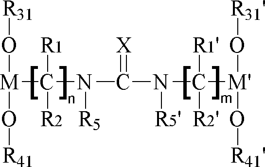
R31, R31’, R41 und R41’ können dabei gleich oder unterschiedlich gewählt sein und sind aus einer Gruppe ausgewählt, die H, gesättigte und ungesättigte Alkylreste, vollständig oder teilweise substituierte, gesättigte und ungesättigte Alkylreste, Aromaten, vollständig oder teilweise substituierte Aromaten, kondensierte Aromaten, vollständig oder teilweise substituierte, kondensierte Aromaten, Heterocyclen, vollständig oder teilweise substituierte Heterocyclen, kondensierte Heterocyclen und vollständig oder teilweise substituierte, kondensierte Heterocyclen umfasst. Bevorzugt sind R31, R31’, R41 und R41’ aus einer Gruppe ausgewählt, die H, gesättigte Alkylreste, vollständig oder teilweise substituierte, gesättigte Alkylreste, Aromaten, vollständig oder teilweise substituierte Aromaten, Heterocyclen und vollständig oder teilweise substituierte Heterocyclen umfasst. Besonders bevorzugt sind R31, R31’, R41 und R41’ aus einer Gruppe ausgewählt, die H, gesättigte Alkylreste und vollständig oder teilweise substituierte, gesättigte Alkylreste umfasst. Gesättigte Alkylreste können beispielsweise Methyl-, Ethyl-, Propyl-, Isopropyl-, Butyl-, Isobutyl-, sec-Butyl-, tert-Butyl- und Cyclohexylreste sein.R31, R31 ', R41 and R41' can be chosen to be identical or different and are selected from a group which condensed H, saturated and unsaturated alkyl radicals, fully or partially substituted, saturated and unsaturated alkyl radicals, aromatics, fully or partially substituted aromatics Aromatic, fully or partially substituted, fused aromatics, heterocycles, fully or partially substituted heterocycles, fused heterocycles, and fully or partially substituted condensed heterocycles. Preferably, R31, R31 ', R41 and R41' are selected from the group comprising H, saturated alkyl radicals, fully or partially substituted, saturated alkyl radicals, aromatics, fully or partially substituted aromatics, heterocycles and fully or partially substituted heterocycles. More preferably, R31, R31 ', R41 and R41' are selected from the group comprising H, saturated alkyl groups and fully or partially substituted, saturated alkyl groups. Saturated alkyl radicals may be, for example, methyl, ethyl, propyl, isopropyl, butyl, isobutyl, sec-butyl, tert-butyl and cyclohexyl radicals.
M’ ist aus einer Gruppe ausgewählt, die B, Al, Si-OR71, Ge-OR71’ und Ti-OR71’’ umfasst, wobei R71, R71’ und R71’’ gleich oder unterschiedlich gewählt sein können und aus der gleichen Gruppe ausgewählt sind wie R31, R31’, R41 und R41’.M 'is selected from a group comprising B, Al, Si-OR71, Ge-OR71' and Ti-OR71 '', wherein R71, R71 'and R71' 'may be the same or different and selected from the same group are such as R31, R31 ', R41 and R41'.
M ist aus einer Gruppe ausgewählt, die B, Al, Si-OR72, Ge-OR72’ und Ti-OR72’’ umfasst. Dabei können R72, R72’ und R72’’ gleich oder unterschiedlich gewählt sein und sind aus der gleichen Gruppe ausgewählt wie R31, R31’, R41 und R41’.M is selected from a group comprising B, Al, Si-OR72, Ge-OR72 'and Ti-OR72' '. Here, R72, R72 'and R72' 'may be the same or different and are selected from the same group as R31, R31', R41 and R41 '.
Umfasst das Auskoppelelement ein Hybridmaterial oder ist das Auskoppelelement aus einem Hybridmaterial hergestellt, das die Reste R71 und R72, R71’ und R72’ oder R71’’ und R72’’ aufweist, können R71 und R72, R71’ und R72’ oder R71’’ und R72’’ gleich gewählt sein.Includes the decoupling element Hybrid material or if the coupling-out element is produced from a hybrid material which has the radicals R71 and R72, R71 'and R72' or R71 '' and R72 '', R71 and R72, R71 'and R72' or R71 '' and R72 '' be chosen equal.
Gemäß einer Ausführungsform sind R31 und R41 und/oder R31’und R41’ gleich gewählt. Umfasst das Auskoppelelement ein Hybridmaterial oder ist das Auskoppelelement aus einem Hybridmaterial hergestellt, das die Reste R71, R71’ oder R71’’ aufweist, können R71, R71’ oder R71’’ den Resten R31’und R41’entsprechen, also identisch gewählt sein. Umfasst das Auskoppelelement ein Hybridmaterial oder ist das Auskoppelelement aus einem Hybridmaterial hergestellt, das die Reste R72, R72’ oder R72’’ aufweist, können R72, R72’ oder R72’’den Resten R31 und R41 entsprechen, also identisch gewählt sein.In one embodiment, R31 and R41 and / or R31 'and R41' are the same. If the decoupling element comprises a hybrid material or if the decoupling element is made of a hybrid material which has the radicals R71, R71 'or R71' ', R71, R71' or R71 '' can correspond to the radicals R31 'and R41', ie be chosen identically. If the decoupling element comprises a hybrid material or if the decoupling element is made of a hybrid material which has the radicals R72, R72 'or R72' ', R72, R72' or R72 '' can correspond to the radicals R31 and R41, ie be chosen identically.
Gemäß einer bevorzugten Ausführungsform ist X aus einer Gruppe ausgewählt, die O und S umfasst. Gemäß einer besonders bevorzugten Ausführungsform ist X = O. In a preferred embodiment, X is selected from a group comprising O and S. According to a particularly preferred embodiment, X = O.
Ein Auskoppelelement, das ein solches Hybridmaterial umfasst oder das aus einem solchen Hybridmaterial hergestellt ist, zeigt eine sehr hohe Stabilität gegenüber Wärme und Strahlung aufgrund der hohen Bindungsstabilität der Harnstofffunktionalität. Die Bindungsenergie der C=O-Doppelbindung liegt bei 708 kJ/mol. Die hohe Stabilität äußert sich dadurch, dass das Auskoppelelement bei einer Einwirkung von Strahlung im sichtbaren, UV und Infrarotbereich des elektromagnetischen Spektrums und bei der Einwirkung von Wärme weder vergilbt noch eintrübt. Die Lebensdauer des optoelektronischen Bauelements ist somit nicht durch das Auskoppelelement limitiert. Des Weiteren weisen solche Auskoppelelemente sehr gute Haftung auf Kunststoffen und Metallen aus. Zudem bietet es eine hohe Elastizität und eine sehr gute Abriebfestigkeit.A decoupling element comprising such a hybrid material or made of such a hybrid material shows a very high stability to heat and radiation due to the high binding stability of the urea functionality. The binding energy of the C = O double bond is 708 kJ / mol. The high stability manifests itself in that the coupling-out element neither yellowing nor clouding under the action of radiation in the visible, UV and infrared range of the electromagnetic spectrum and under the action of heat. The service life of the optoelectronic component is therefore not limited by the outcoupling element. Furthermore, such decoupling elements have very good adhesion to plastics and metals. It also offers high elasticity and very good abrasion resistance.
Gemäß einer Ausführungsform sind M und M’ aus einer Gruppe ausgewählt, die Si-R7 und Al umfasst. Besonders bevorzugt sind M und M’ gleich Si-R7. In one embodiment, M and M 'are selected from a group comprising Si-R7 and Al. Most preferably, M and M 'are Si-R7.
Gemäß einer Ausführungsform umfasst das zumindest eine Auskoppelelement ein Hybridmaterial oder ist aus einem Hybridmaterial hergestellt, das folgende Struktur aufweist: 
Gemäß einer Ausführungsform sind R1, R1', R2, R2' aus einer Gruppe ausgewählt, die H, gesättigte Alkylreste, vollständig oder teilweise substituierte gesättigte Alkylreste, Aromaten und vollständig oder teilweise substituierte Aromaten, umfasst. Beispielsweise können R1, R1', R2, R2' Methyl-, Ethyl-, Propyl-, Isopropyl-, Butyl-, Isobutyl-, sec-Butyl-, tert-Butyl-, Cyclohexyl- oder Phenylreste sein. Besonders bevorzugt sind R1, R1', R2, R2' gleich H. In one embodiment, R1, R1 ', R2, R2' are selected from a group comprising H, saturated alkyl radicals, fully or partially substituted saturated alkyl radicals, aromatics, and fully or partially substituted aromatics. For example, R1, R1 ', R2, R2' may be methyl, ethyl, propyl, isopropyl, butyl, isobutyl, sec-butyl, tert-butyl, cyclohexyl or phenyl. R1, R1 ', R2, R2' are particularly preferably H.
Die Reste R1 und R1’ und/oder R2 und R2’ können gleich gewählt sein. Möglich ist auch, dass die Reste und R1 und R2 und/oder R1’und R2’ gleich gewählt sind.The radicals R1 and R1 'and / or R2 and R2' can be chosen the same. It is also possible that the radicals and
Gemäß einer Ausführungsform sind R5 und R5' aus einer Gruppe ausgewählt, die H, gesättigte Alkylreste und vollständig oder teilweise substituierte gesättigte Alkylreste umfasst. Beispielsweise können R5 und R5' Methyl-, Ethyl-, Propyl-, Isopropyl-, Butyl-, Isobutyl-, sec-Butyl-, tert-Butyl-, Cyclohexyl- oder Phenylreste sein. R5 und R5' können gleich oder unterschiedlich gewählt sein. Besonders bevorzugt sind R5 und R5' gleich H.In one embodiment,
Das optoelektronischen Bauelement kann eine Lumineszenzdiode, ein Fotodioden-Transistoren-Array/Modul und ein optischer Koppler sein. Alternativ ist das optoelektronische Bauelement eine organische Leuchtdiode (OLED). Insbesondere kann es sich bei dem optoelektronischen Bauelement um eine LED mit einer elektrischen Leistung von einem Watt und mehr handeln. The optoelectronic component may be a light emitting diode, a photodiode transistor array / module and an optical coupler. Alternatively, the optoelectronic component is an organic light-emitting diode (OLED). In particular, the optoelectronic component can be an LED with an electrical power of one watt and more.
Gemäß einer Ausführungsform umfasst das zumindest eine transparente Auskoppelelement Konverterpartikel. Die Konverterpartikel sind in dem Auskoppelelement verteilt und konvertieren zumindest teilweise die elektromagnetische Primärstrahlung in eine elektromagnetische Sekundärstrahlung. According to one embodiment, the at least one transparent decoupling element comprises converter particles. The converter particles are distributed in the decoupling element and at least partially convert the electromagnetic primary radiation into an electromagnetic secondary radiation.
Zumindest teilweise bedeutet, dass die elektromagnetische Primärstrahlung zumindest teilweise von den Konverterpartikeln absorbiert und als elektromagnetische Sekundärstrahlung mit einem von der elektromagnetischen Primärstrahlung verschiedenen Wellenlängenbereich emittiert wird. Die elektromagnetische Primärstrahlung und/oder elektromagnetische Sekundärstrahlung können eine oder mehrere Wellenlängen und/oder Wellenlängenbereiche in einem infraroten bis ultravioletten Wellenlängenbereich umfassen, insbesondere in einem sichtbaren Wellenlängenbereich. Dabei können die Spektren der Primärstrahlung und/oder der Sekundärstrahlung schmalbandig sein, das heißt, dass die Primärstrahlung und/oder die Sekundärstrahlung dann einen einfarbigen oder annähernd einfarbigen Wellenlängenbereich aufweisen. Das Spektrum der Primärstrahlung und/oder das Spektrum der Sekundärstrahlung kann alternativ auch breitbandig sein, das heißt, dass die Primärstrahlung und/oder die Sekundärstrahlung einen mischfarbigen Wellenlängenbereich aufweisen kann, wobei der mischfarbige Wellenlängenbereich ein kontinuierliches Spektrum oder mehrere diskrete spektrale Komponenten mit verschiedenen Wellenlängen aufweisen kann. At least partially means that the electromagnetic primary radiation is at least partially absorbed by the converter particles and emitted as electromagnetic secondary radiation having a different wavelength range from the electromagnetic primary radiation. The electromagnetic primary radiation and / or secondary electromagnetic radiation may comprise one or more wavelengths and / or wavelength ranges in an infrared to ultraviolet wavelength range, in particular in a visible wavelength range. In this case, the spectra of the primary radiation and / or the secondary radiation may be narrow-band, that is to say that the primary radiation and / or the secondary radiation then have a monochrome or approximately monochromatic wavelength range. The spectrum of the primary radiation and / or the spectrum of the secondary radiation may alternatively also be broadband, that is to say that the primary radiation and / or the secondary radiation may have a mixed-color wavelength range, the mixed-color wavelength range being a continuous spectrum or a plurality of discrete ones spectral components with different wavelengths may have.
Die Primärstrahlung und die Sekundärstrahlung können überlagert einen weißfarbigen Leuchteindruck erwecken. Dazu kann die Primärstrahlung vorzugsweise einen blaufarbigen Leuchteindruck erwecken und die Sekundärstrahlung einen gelbfarbigen Leuchteindruck, der durch spektrale Komponenten der Sekundärstrahlung im gelben Wellenlängenbereich und/oder spektrale Komponenten im grünen und roten Wellenlängenbereich entstehen kann. The primary radiation and the secondary radiation can superimpose a white-colored luminous impression. For this purpose, the primary radiation can preferably give rise to a blue-colored luminous impression and the secondary radiation can produce a yellowish-colored luminous impression, which can result from spectral components of the secondary radiation in the yellow wavelength range and / or spectral components in the green and red wavelength ranges.
Es ist auch möglich, dass die elektromagnetische Primärstrahlung vollständig oder nahezu vollständig in eine elektromagnetische Sekundärstrahlung konvertiert. Die elektromagnetische Primärstrahlung wird hierbei vollständig oder nahezu vollständig durch das Konvertermaterial absorbiert wird und in Form einer elektromagnetischen Sekundärstrahlung emittiert. Die emittierte Strahlung des optoelektronischen Bauelements gemäß dieser Ausführungsform entspricht somit vollständig oder nahezu vollständig der elektromagnetischen Sekundärstrahlung. Unter nahezu vollständiger Konversion ist eine Konversion über 90 %, insbesondere über 95 % zu verstehen. It is also possible that the electromagnetic primary radiation completely or almost completely converted into an electromagnetic secondary radiation. The electromagnetic primary radiation is in this case completely or almost completely absorbed by the converter material and emitted in the form of electromagnetic secondary radiation. The emitted radiation of the optoelectronic component according to this embodiment thus corresponds completely or almost completely to the electromagnetic secondary radiation. Nearly complete conversion is a conversion over 90%, especially over 95% to understand.
Es ist möglich, dass die Primärstrahlung im UV-Bereich liegt und die Sekundärstrahlung einen blaufarbigen und gelbfarbigen Leuchteindruck erweckt, der durch spektrale Komponenten der Sekundärstrahlung im blauen und im gelben Wellenlängenbereich und/oder spektrale Komponenten im blauen, grünen und roten Wellenlängenbereich entstehen kann. Hier kann die Sekundärstrahlung einen weißfarbigen Leuchteindruck erwecken.It is possible that the primary radiation is in the UV range and the secondary radiation gives rise to a blue-colored and yellow-colored luminous impression, which can be caused by spectral components of the secondary radiation in the blue and yellow wavelength range and / or spectral components in the blue, green and red wavelength range. Here, the secondary radiation can create a white-colored luminous impression.
Gemäß einer Ausführungsform liegt die elektromagnetische Sekundärstrahlung in einem blauen bis infraroten Wellenlängenbereich.According to one embodiment, the electromagnetic secondary radiation lies in a blue to infrared wavelength range.
Gemäß einer Ausführungsform weist das Auskoppelelement eine Transparenz von über 95 % für die emittierte Sekundärstrahlung auf, besonders bevorzugt liegt die Transparenz des Auskoppelelements bei über 98 % für die emittierte Sekundärstrahlung.According to one embodiment, the decoupling element has a transparency of more than 95% for the emitted secondary radiation, particularly preferably the transparency of the decoupling element is more than 98% for the emitted secondary radiation.
Gemäß einer Ausführungsform des optoelektronischen Bauelements weisen die Konverterpartikel einen Partikeldurchmesser von 1 bis 20 µm auf. Bevorzugt weisen die Konverterpartikel einen Partikeldurchmesser von 5 bis 15 µm, besonders bevorzugt von 10 µm auf. According to one embodiment of the optoelectronic component, the converter particles have a particle diameter of 1 to 20 μm. Preferably, the converter particles have a particle diameter of 5 to 15 .mu.m, more preferably of 10 .mu.m.
Die Konverterpartikel können beispielsweise aus einem der folgenden Leuchtstoffe gebildet sein: mit Metallen der seltenen Erden dotierte Granate, mit Metallen der seltenen Erden dotierte Erdalkalisulfide, mit Metallen der seltenen Erden dotierte Thiogallate, mit Metallen der seltenen Erden dotierte Aluminate, mit Metallen der seltenen Erden dotierte Silicate, wie Orthosilicate, mit Metallen der seltenen Erden dotierte Chlorosilicate, mit Metallen der seltenen Erden dotierte Erdalkalisiliziumnitride, mit Metallen der seltenen Erden dotierte Oxinitride und mit Metallen der seltenen Erden dotierte Aluminiumoxinitride, mit Metallen der seltenen Erden dotierte Siliziumnitride, Sialone.The converter particles may be formed, for example, from one of the following phosphors: rare earth doped garnets, rare earth doped alkaline earth sulfides, rare earth doped thiogallates, rare earth doped aluminates, rare earth doped metals Silicates, such as orthosilicates, rare earth doped chlorosilicates, rare earth doped alkaline earth silicon nitrides, rare earth doped oxynitrides and rare earth doped aluminum oxynitrides, rare earth doped silicon nitrides, sialons.
Als Leuchtstoffe können insbesondere Granate, wie Yttriumaluminiumoxid (YAG), Lutetiumaluminiumoxid (LuAG) und Terbiumaluminiumoxid (TAG) verwendet werden.In particular, garnets such as yttrium aluminum oxide (YAG), lutetium aluminum oxide (LuAG) and terbium aluminum oxide (TAG) can be used as phosphors.
Die Leuchtstoffe sind beispielsweise mit einem der folgenden Aktivatoren dotiert: Cer, Europium, Terbium, Praseodym, Samarium, Mangan.The phosphors are, for example, doped with one of the following activators: cerium, europium, terbium, praseodymium, samarium, manganese.
Gemäß einer weiteren Ausführungsform umfasst das Auskoppelelement Konverterpartikel verschiedener Leuchtstoffe.According to a further embodiment, the decoupling element comprises converter particles of different phosphors.
Gemäß einer Ausführungsform liegen die Konverterpartikel zu 1 bis 50 Vol-% in Bezug auf das Hybridmaterial vor. Bevorzugt sind 10 bis 40 Vol-%, besonders bevorzugt sind 20 bis 30 Vol-%. In one embodiment, the converter particles are present at 1 to 50% by volume with respect to the hybrid material. Preference is given to 10 to 40% by volume, more preferably 20 to 30% by volume.
Gemäß einer Ausführungsform sind die Konverterpartikel homogen in dem Auskoppelelement verteilt. Durch eine homogene Verteilung der Konverterpartikel ist eine gleichmäßige Konversion der Primärstrahlung durch die Konverterpartikel möglich, was eine gleichmäßige Abstrahlcharakteristik der Sekundärstrahlung zur Folge hat.According to one embodiment, the converter particles are distributed homogeneously in the outcoupling element. Due to a homogeneous distribution of the converter particles, a uniform conversion of the primary radiation by the converter particles is possible, which results in a uniform emission characteristic of the secondary radiation.
Gemäß einer Ausführungsform ist das zumindest eine Auskoppelelement aus dem Hybridmaterial hergestellt und die Konverterpartikel sind durch chemische Bindungen an das Hybridmaterial gebunden. Unter chemischen Bindungen können kovalente Bindungen, Ionenbindungen oder auch koordinative Bindungen zwischen den Konverterpartikeln und dem Hybridmaterial verstanden werden.According to one embodiment, the at least one outcoupling element is made of the hybrid material and the converter particles are bonded to the hybrid material by chemical bonds. Chemical bonds can be understood as meaning covalent bonds, ionic bonds or coordinative bonds between the converter particles and the hybrid material.
Gemäß einer Ausführungsform umfasst das zumindest eine Auskoppelelement Nanopartikel. According to one embodiment, the at least one decoupling element comprises nanoparticles.
Gemäß einer Ausführungsform sind die Nanopartikel kleiner als ein Zehntel der Wellenlänge der emittierten Primärstrahlung der aktiven Schicht der Schichtenfolge. Die Nanopartikel können eine Größe von 10 bis 25 nm, 10 bis 20 nm, besonders bevorzugt 10 bis 15 nm aufweisen. In dieser Größenordnung streuen die Nanopartikel die Primärstrahlung und/oder Sekundärstrahlung nicht. According to one embodiment, the nanoparticles are smaller than a tenth of the wavelength of the emitted primary radiation of the active layer of the layer sequence. The nanoparticles may have a size of 10 to 25 nm, 10 to 20 nm, more preferably 10 to 15 nm. On this scale, the nanoparticles do not scatter the primary radiation and / or secondary radiation.
Gemäß einer Ausführungsform umfassen die Nanopartikel thermisch leitfähige Materialien. According to one embodiment, the nanoparticles comprise thermally conductive materials.
Gemäß einer Ausführungsform sind die thermisch leitfähigen Materialien aus einer Gruppe ausgewählt, die Al2O3, AlN, SiO2 und Kombinationen daraus umfasst According to one embodiment, the thermally conductive materials are selected from a group comprising Al 2 O 3 , AlN, SiO 2 and combinations thereof
Durch thermisch leitfähigen Materialien entsteht kein Wärmestau in dem Auskoppelelement und es kann eine konstante Leuchtstärke und ein konstanter Farbort über die Länge der Betriebsdauer des optoelektronischen Bauelements garantiert werden. Somit kann einem frühzeitigen Ausfall des optoelektronischen Bauelements vorgebeugt werden und die Lebensdauer des optoelektronischen Bauelements verlängert werden.By thermally conductive materials no heat accumulation in the decoupling element and it can be guaranteed a constant luminous intensity and a constant color location over the length of the operating life of the optoelectronic device. Thus, an early failure of the optoelectronic device can be prevented and the life of the optoelectronic device can be extended.
Gemäß einer Ausführungsform umfassen die Nanopartikeln Füllstoffe, die einen Brechungsindex nD bei 23 °C von größer oder gleich 2 aufweisen.According to one embodiment, the nanoparticles comprise fillers which have a refractive index n D at 23 ° C. of greater than or equal to 2.
Auskoppelelemente, die Füllstoffe mit einem Brechungsindex nD bei 23 °C von größer oder gleich 2 aufweisen, zeigen eine erhöhte Lichtauskopplung, da Lichtverluste durch Reflexion und Totalreflexion weitgehend vermieden werden können. Die Lichtauskopplung ist besonders hoch, wenn der Brechungsindex des Auskoppelelements einen ähnlichen Brechungsindex aufweist, wie die an das Auskoppelelement angrenzenden Schichten innerhalb des Strahlengangs des Bauelements.Decoupling elements having fillers with a refractive index n D at 23 ° C of greater than or equal to 2, show an increased light outcoupling, since light losses due to reflection and total reflection can be largely avoided. The light outcoupling is particularly high when the refractive index of the coupling-out element has a similar refractive index as the layers adjacent to the coupling-out element within the beam path of the component.
Die Füllstoffe können aus einer Gruppe ausgewählt sein, die ZrO2, TiO2, Nb2O5, Ta2O5 und Kombinationen daraus umfasst. Bevorzugt ist der Füllstoff ZrO2. The fillers can be selected from a group consisting of ZrO 2, TiO 2, Nb 2 O 5, Ta 2 O 5 and combinations thereof. The filler is preferably ZrO 2 .
Durch ionische Wechselwirkungen können die Nanopartikel an das Hybridmaterial gebunden sein. Insbesondere wenn M und/oder M’ gleich Si-R7 kann durch besonders starke ionische Wechselwirkungen des Siliziums des Hybridmaterials mit den Nanopartikeln, insbesondere mit ZrO2 eine sehr starke Anbindung der Nanopartikel an das Hybridmaterial erfolgen.By ionic interactions, the nanoparticles can be bound to the hybrid material. In particular, if M and / or M 'is equal to Si-R7, a particularly strong binding of the nanoparticles to the hybrid material can occur due to particularly strong ionic interactions of the silicon of the hybrid material with the nanoparticles, in particular with ZrO 2 .
Es ist möglich, dass in dem Auskoppelelement verschiedene Nanopartikel vorhanden sind. Beispielsweise kann ein thermisch leitfähiges Material und ein Füllstoff, der einen Brechungsindex nD bei 23 °C von größer oder gleich 2 aufweist, vorhanden sein.It is possible that different nanoparticles are present in the decoupling element. For example, a thermally conductive material and a filler having a refractive index n D at 23 ° C of greater than or equal to 2 may be present.
Gemäß einer Ausführungsform sind die Nanopartikel homogen in dem Auskoppelelement verteilt, woraus eine gleichmäßige Abstrahlcharakteristik der Sekundärstrahlung und/oder der Primärstrahlung resultiert.According to one embodiment, the nanoparticles are homogeneously distributed in the outcoupling element, resulting in a uniform emission characteristic of the secondary radiation and / or the primary radiation.
In einer Ausführungsform umfasst das optoelektronische Bauelement ein Gehäuse. In dem Gehäuse kann insbesondere in der Mitte eine Ausnehmung vorhanden sein. Die Schichtenfolge kann in der Ausnehmung angeordnet sein. Es ist möglich, dass die Ausnehmung mit der Schichtenfolge mit einem Verguss ausgefüllt ist. In one embodiment, the optoelectronic component comprises a housing. In the housing may be present in particular in the middle of a recess. The layer sequence can be arranged in the recess. It is possible that the recess is filled with the layer sequence with a potting.
In einer Ausführungsform ist das Auskoppelelement als Verguss ausgebildet. Der Verguss kann die Ausnehmung in dem Gehäuse ausfüllen. In one embodiment, the decoupling element is designed as a potting. The potting can fill the recess in the housing.
Gemäß einer Ausführungsform ist das Auskoppelelement als ein Plättchen ausgebildet, das über der Schichtenfolge angeordnet ist. Es ist möglich, dass das Plättchen die gesamte Oberfläche der Schichtenfolge bedeckt. According to one embodiment, the decoupling element is designed as a small plate, which is arranged above the layer sequence. It is possible that the plate covers the entire surface of the layer sequence.
Dass eine Schicht oder ein Element "auf" oder "über" einer anderen Schicht oder einem anderen Element angeordnet oder aufgebracht ist, kann dabei hier und im Folgenden bedeuten, dass die eine Schicht oder das eine Element unmittelbar in direktem mechanischen und/oder elektrischen Kontakt auf der anderen Schicht oder dem anderen Element angeordnet ist. Weiter kann es auch bedeuten, dass die eine Schicht oder das eine Element mittelbar auf beziehungsweise über der anderen Schicht oder dem anderen Element angeordnet ist. Dabei können dann weitere Schichten und/oder Elemente oder ein lichter Abstand zwischen der einen oder der anderen Schicht beziehungsweise zwischen dem einen oder dem anderen Element angeordnet sein. The fact that a layer or an element is arranged or applied "on" or "above" another layer or another element can mean here and below that the one layer or the one element directly in direct mechanical and / or electrical contact is arranged on the other layer or the other element. Furthermore, it can also mean that the one layer or the one element is arranged indirectly on or above the other layer or the other element. In this case, further layers and / or elements or a clear distance can then be arranged between the one or the other layer or between the one or the other element.
Gemäß einer weiteren Ausführungsform ist das Auskoppelelement eine Linse. Es ist möglich, dass die Linse über einem Verguss angeordnet ist. Es ist ein direkter mechanischer Kontakt zwischen der Linse und dem Verguss möglich.According to a further embodiment, the decoupling element is a lens. It is possible that the lens is placed over a potting. There is a direct mechanical contact between the lens and the potting possible.
In einer weiteren Ausführungsform umfasst das optoelektronische Bauelement zwei Auskoppelelemente. In a further embodiment, the optoelectronic component comprises two outcoupling elements.
Bei dem ersten Auskoppelelement kann es sich hierbei um einen Verguss handeln, der das Hybridmaterial umfasst oder der aus dem Hybridmaterial hergestellt ist. Das zweite Auskoppelelement kann ein Plättchen, angeordnet über der Schichtenfolge sein, das das Hybridmaterial umfasst oder aus dem Hybridmaterial hergestellt ist. The first outcoupling element may be a potting compound comprising the hybrid material or made of the hybrid material. The second outcoupling element may be a plate, arranged above the layer sequence comprising the hybrid material or made of the hybrid material.
Es ist auch möglich, dass das zweite Auskoppelelement eine Linse ist, die aus dem Hybridmaterial hergestellt ist oder das Hybridmaterial umfasst. It is also possible that the second outcoupling element is a lens made of the hybrid material or comprising the hybrid material.
Möglich ist auch, dass das erste Auskoppelelement ein Plättchen, angeordnet über der Schichtenfolge ist, das aus dem Hybridmaterial hergestellt ist oder das Hybridmaterial umfasst. It is also possible that the first decoupling element is a plate, arranged over the layer sequence, which is made of the hybrid material or comprises the hybrid material.
Das erste und das zweite Auskoppelelement können die gleichen Hybridmaterialien umfassen oder aus dem gleichen Hybridmaterial hergestellt sein. The first and the second decoupling element may be the same hybrid materials or made from the same hybrid material.
Vorzugsweise umfassen das erste und das zweite Auskoppelelement unterschiedliche Hybridmaterialien oder sind aus unterschiedlichen Hybridmaterialien hergestellt. Preferably, the first and the second outcoupling element comprise different hybrid materials or are made of different hybrid materials.
Es ist möglich, dass das erste und das zweite Auskoppelelement gleiche oder unterschiedliche Konverterpartikel umfassen. It is possible that the first and the second outcoupling element comprise the same or different converter particles.
Gemäß einer weiteren Ausführungsform umfasst das optoelektronische Bauelement mindestens eine zweite Schichtenfolge. According to a further embodiment, the optoelectronic component comprises at least one second layer sequence.
Es ist möglich, dass über der zweiten und jeder weiteren Schichtenfolge Auskoppelelemente in Form eines Plättchens aufgebracht sind. It is possible that decoupling elements in the form of a small plate are applied over the second and each further layer sequence.
In einer Ausführungsform hat das Plättchen eine Dicke von 10 µm bis 100 µm, bevorzugt 20 µm bis 50 µm, besonders bevorzugt 30 µm bis 40 µm. In one embodiment, the platelet has a thickness of 10 μm to 100 μm, preferably 20 μm to 50 μm, particularly preferably 30 μm to 40 μm.
Es ist möglich, dass über dem Plättchen ein Verguss angeordnet ist. Der Verguss kann aus herkömmlichen Vergussmaterialien ausgewählt sein. It is possible that a potting is arranged above the plate. The potting may be selected from conventional potting materials.
Gemäß einer Ausführungsform ist eine Haftschicht zwischen der Schichtenfolge und dem Plättchen angeordnet. According to one embodiment, an adhesion layer is arranged between the layer sequence and the platelet.
Es ist möglich, dass zwischen dem Verguss und der Linse eine Haftschicht angeordnet ist. It is possible that an adhesive layer is disposed between the potting and the lens.
Üblicherweise sind Haftschichten jedoch nicht nötig, da die Plättchen, Linsen und Vergüsse umfassend das Hybridmaterial oder die Plättchen, Linsen und Vergüsse, die aus dem Hybridmaterial hergestellt sind, eine sehr gute Haftfestigkeit zu den angrenzenden Schichten oder Elementen aufweisen. Insbesondere ist die Haftfestigkeit zu angrenzenden Schichten oder Elementen sehr hoch, wenn diese Kunststoffe oder Metalle umfassen.However, adhesive layers are usually not necessary because the platelets, lenses and molds comprising the hybrid material or the platelets, lenses and molds made of the hybrid material have very good adhesion to the adjacent layers or elements. In particular, the adhesion to adjacent layers or elements is very high when they include plastics or metals.
Dass eine Schicht oder ein Element zwischen zwei anderen Schichten oder Elementen angeordnet ist, kann hier und im Folgenden bedeuten, dass die eine Schicht oder das eine Element unmittelbar im direkten mechanischen und/oder elektrischen Kontakt oder im mittelbaren Kontakt zu einem der zwei anderen Schichten oder Elementen und in direktem mechanischen und/oder elektrischen Kontakt oder in mittelbarem Kontakt zu anderen der zwei anderen Schichten oder Elementen angeordnet ist. Dabei können bei mittelbarem Kontakt dann weitere Schichten und/oder Elemente oder ein lichter Abstand zwischen der einen und zumindest einer der zwei anderen Schichten beziehungsweise zwischen dem einen und zumindest einem der zwei anderen Elemente angeordnet sein. The fact that a layer or an element is arranged between two other layers or elements may mean here and in the following that the one layer or the element directly in direct mechanical and / or electrical contact or in indirect contact with one of the two other layers Elements and in direct mechanical and / or electrical contact or in indirect contact with others of the other two layers or elements is arranged. In the case of indirect contact, further layers and / or elements or a clear distance between the one and at least one of the two other layers or between the one and at least one of the two other elements can then be arranged.
In einer Ausführungsform ist das Gehäuse aus einem Hybridmaterial hergestellt, das folgende Struktur aufweist: 
R1, R1’ R2, R2’ und R5 können gleich oder unterschiedlich gewählt sein und sind aus einer Gruppe ausgewählt, die H, gesättigte und ungesättigte Alkylreste, vollständig oder teilweise substituierte, gesättigte und ungesättigte Alkylreste, Aromaten, vollständig oder teilweise substituierte Aromaten, Heterocyclen und vollständig oder teilweise substituierte Heterocyclen umfasst.R1, R1 'R2, R2' and R5 may be the same or different and are selected from the group consisting of H, saturated and unsaturated alkyl radicals, fully or partially substituted, saturated and unsaturated alkyl radicals, aromatics, fully or partially substituted aromatics, heterocycles and fully or partially substituted heterocycles.
R3, R3’, R4 und R4’ können gleich oder unterschiedlich gewählt sein und sind aus einer Gruppe ausgewählt, die H, gesättigte und ungesättigte Alkylreste, vollständig oder teilweise substituierte, gesättigte und ungesättigte Alkylreste, Alkoxygruppen, Aryloxygruppen, Amine, Amide, Ester, Aromaten, vollständig oder teilweise substituierte Aromaten, Heterocyclen und vollständig oder teilweise substituierte Heterocyclen umfasst.R3, R3 ', R4 and R4' may be selected the same or different and are selected from the group consisting of H, saturated and unsaturated alkyl radicals, fully or partially substituted, saturated and unsaturated alkyl radicals, alkoxy groups, aryloxy groups, amines, amides, esters, Aromatics, fully or partially substituted aromatics, heterocycles, and fully or partially substituted heterocycles.
X ist aus einer Gruppe ausgewählt, die O, S und N-R6 umfasst, wobei R6 aus der gleichen Gruppe ausgewählt ist wie R1, R1’ R2, R2’ und R5.X is selected from a group comprising O, S and N-R6, wherein R6 is selected from the same group as R1, R1 'R2, R2' and R5.
M und M’ können gleich oder unterschiedlich gewählt sein und sind aus einer Gruppe ausgewählt, die B, Al, Si-R7, Ge-R7’ und Ti-R7’’ umfasst. R7, R7’ und R7’’ können dabei gleich oder unterschiedlich gewählt sein und sind aus der gleichen Gruppe ausgewählt wie R3, R3’, R4 und R4’. M and M 'may be the same or different and are selected from a group comprising B, Al, Si-R7, Ge-R7' and Ti-R7 ''. R7, R7 'and R7' 'may be chosen the same or different and are selected from the same group as R3, R3', R4 and R4 '.
Y ist aus einer Gruppe ausgewählt, die O, S, N-R5’ und eine Bindung umfasst, wobei R5’ aus der gleichen Gruppe ausgewählt ist wie R1, R1’ R2, R2’ und R5 und gleich oder unterschiedlich wie R1, R1’ R2, R2’ ausgewählt sein kann. Dass Y eine Bindung sein kann bedeutet, dass eine Verbindung folgender Formel vorliegt: 
n, m können gleich oder unterschiedlich gewählt sein, wobei und 1 ≤ n, m ≤ 10000. Bevorzugt ist 1 ≤ n, m ≤ 5000, besonders bevorzugt ist 1 ≤ n, m ≤ 1000.n, m can be chosen to be the same or different, where and 1 ≦ n, m ≦ 10000. Preference is given to 1 ≦ n, m ≦ 5000, more preferably 1 ≦ n, m ≦ 1000.
Gemäß einer Ausführungsform ist das Gehäuse aus einem Hybridmaterial hergestellt, das folgende Struktur aufweist: 
- – R1, R1’ R2, R2’, R5 und R5’ gleich oder unterschiedlich gewählt sein können und aus einer Gruppe ausgewählt sind, die H, gesättigte und ungesättigte Alkylreste, vollständig oder teilweise substituierte, gesättigte und ungesättigte Alkylreste, Aromaten, vollständig oder teilweise substituierte Aromaten, Heterocyclen und vollständig oder teilweise substituierte Heterocyclen umfasst,
- – R3, R3’, R4 und R4’ gleich oder unterschiedlich gewählt sein können und aus einer Gruppe ausgewählt sind, die H, gesättigte und ungesättigte Alkylreste, vollständig oder teilweise substituierte, gesättigte und ungesättigte Alkylreste, Alkoxygruppen, Aryloxygruppen, Amine, Amide, Ester, Aromaten, vollständig oder teilweise substituierte Aromaten, Heterocyclen und vollständig oder teilweise substituierte Heterocyclen umfasst,
- – X aus einer Gruppe ausgewählt ist, die O, S und N-R6 umfasst,
- – R6 aus der gleichen Gruppe ausgewählt ist wie R1, R1’ R2, R2’, R5 und R5’,
- – M und M’ gleich oder unterschiedlich gewählt sein können und aus einer Gruppe ausgewählt sind, die B, Al, Si-R7, Ge-R7’ und Ti-R7’’ umfasst,
- – R7, R7’ und R7’’ gleich oder unterschiedlich gewählt sein können und aus der gleichen Gruppe ausgewählt sind wie R3, R3’, R4 und R4’ und
- – n, m können gleich oder unterschiedlich gewählt sein können und 1 ≤ n, m ≤ 1000.
- - R1, R1 'R2, R2', R5 and R5 'may be the same or different and are selected from a group comprising H, saturated and unsaturated alkyl radicals, fully or partially substituted, saturated and unsaturated alkyl radicals, aromatics, in whole or in part comprises substituted aromatics, heterocycles and fully or partially substituted heterocycles,
- - R3, R3 ', R4 and R4' may be the same or different and are selected from a group comprising H, saturated and unsaturated alkyl radicals, fully or partially substituted, saturated and unsaturated alkyl radicals, alkoxy groups, aryloxy groups, amines, amides, esters , Aromatics, fully or partially substituted aromatics, heterocycles and fully or partially substituted heterocycles,
- X is selected from a group comprising O, S and N-R6,
- R6 is selected from the same group as R1, R1 'R2, R2', R5 and R5 ',
- M and M 'may be the same or different and are selected from a group comprising B, Al, Si-R7, Ge-R7' and Ti-R7 '',
- - R7, R7 'and R7''may be the same or different and are selected from the same group as R3, R3', R4 and R4 'and
- - n, m can be the same or different and 1 ≤ n, m ≤ 1000.
Bevorzugt ist das Gehäuse aus einem Hybridmaterial hergestellt, das folgende Struktur aufweist: 
Unter Alkylresten mit endständigen C=C-Doppelbindungen versteht man, dass die Alkylreste an einem von der Anbindung an den Sauerstoff entfernten Ende ihrer Kette eine C=C-Doppelbindung aufweisen, wobei eines der C-Atome, das an der Doppelbindung beteiligt ist, eine CH2-Gruppe oder ein C-Atom mit zwei Alkyl- oder Arylresten ist. Alkyl radicals having terminal C =C double bonds are understood to mean that the alkyl radicals have a C =C double bond at one end of their chain remote from the oxygen bond, with one of the C atoms participating in the double bond forming a C =C double bond CH 2 group or a C atom having two alkyl or aryl radicals.
Durch den Einsatz von Hybridmaterialien, die ungesättigte Alkylreste mit endständigen C=C-Doppelbindungen und teilweise substituierte ungesättigte Alkylreste mit endständigen C=C-Doppelbindungen aufweisen, können die Hybridmaterialien weiter polymerisieren. So kann die chemische und physikalische Beständigkeit des Materials erhöht werden, da ein dreidimensionales Netzwerk entsteht, so dass das Material auch für ein Gehäuse eingesetzt werden kann.By using hybrid materials having unsaturated C = C double-bond alkyl radicals and partially substituted unsaturated C = C-terminated alkyl radicals, the hybrid materials can further polymerize. Thus, the chemical and physical resistance of the material can be increased because of a three-dimensional network, so that the material can also be used for a housing.
Bevorzugt ist das Gehäuse aus einem Hybridmaterial hergestellt, wobei R31, R31’, R41, R41, R71 und R71’ folgende Struktur aufweisen: ![]()
![]()
Gemäß einer Ausführungsform ist das Gehäuse zumindest im Bereich der Ausnehmung reflektierend ausgebildet.According to one embodiment, the housing is formed reflecting at least in the region of the recess.
Gemäß einer Ausführungsform umfasst das Gehäuse Weißpigmente. Die Weißpigmente werden dafür verwendet, das Gehäuse beziehungsweise Teilbereiche des Gehäuses einzufärben. Durch das Einfärben kann beispielsweise die Reflektivität und die Strahlenbeständigkeit des Gehäuses erhöht werden.According to one embodiment, the housing comprises white pigments. The white pigments are used to color the housing or parts of the housing. By coloring, for example, the reflectivity and the radiation resistance of the housing can be increased.
Gemäß einer Ausführungsform sind die Weißpigmente aus einer Gruppe ausgewählt, die Titandioxid, Lithopone, Bariumsulfat, Zinkoxid, Zinksulfid, Bleicarbonat, Calciumcarbonat und Kombinationen daraus umfasst. In one embodiment, the white pigments are selected from the group consisting of titanium dioxide, lithopone, barium sulfate, zinc oxide, zinc sulfide, lead carbonate, calcium carbonate, and combinations thereof.
Weitere vorteilhafte Ausführungsformen und Weiterbildungen der Erfindung ergeben sich aus den im Folgenden und in Verbindung mit den Figuren beschriebenen Ausführungsbeispielen. Further advantageous embodiments and developments of the invention will become apparent from the embodiments described below and in conjunction with the figures.
Das optoelektronische Bauelement 
Das Plättchen
Vorzugsweise handelt es sich bei dem optoelektronischen Bauelement
Das optoelektronische Bauelement gemäß 
Der Verguss
Vorzugsweise handelt es sich bei dem optoelektronischen Bauelement
Das optoelektronische Bauelement gemäß 
Der Verguss
Vorzugsweise handelt es sich bei dem optoelektronischen Bauelement
Die Erfindung ist nicht durch die Beschreibung anhand der Ausführungsbeispiele beschränkt. Vielmehr umfasst die Erfindung jedes neue Merkmal sowie jede Kombination von Merkmalen, was insbesondere jede Kombination von Merkmalen in den Patentansprüchen beinhaltet, auch wenn dieses Merkmal oder diese Kombination selbst nicht explizit in den Patentansprüchen oder Ausführungsbeispielen angegeben ist. The invention is not limited by the description with reference to the embodiments. Rather, the invention encompasses any novel feature as well as any combination of features, including in particular any combination of features in the claims, even if this feature or combination itself is not explicitly stated in the claims or exemplary embodiments.
Claims (16)


Priority Applications (6)
| Application Number | Priority Date | Filing Date | Title |
|---|---|---|---|
| DE102012108939.6A DE102012108939A1 (en) | 2012-09-21 | 2012-09-21 | Optoelectronic component comprising a transparent coupling-out element |
| PCT/EP2013/069608 WO2014044813A2 (en) | 2012-09-21 | 2013-09-20 | Optoelectronic component comprising a transparent coupling-out element |
| DE112013004622.9T DE112013004622A5 (en) | 2012-09-21 | 2013-09-20 | Optoelectronic component comprising a transparent coupling-out element |
| US14/430,191 US9515236B2 (en) | 2012-09-21 | 2013-09-20 | Optoelectronic component comprising a transparent coupling-out element |
| JP2015532428A JP6127145B2 (en) | 2012-09-21 | 2013-09-20 | Optoelectronic components including transparent light extraction elements |
| CN201380049400.5A CN104662681B (en) | 2012-09-21 | 2013-09-20 | Include the opto-electronic device of transparent coupling elements |
Applications Claiming Priority (1)
| Application Number | Priority Date | Filing Date | Title |
|---|---|---|---|
| DE102012108939.6A DE102012108939A1 (en) | 2012-09-21 | 2012-09-21 | Optoelectronic component comprising a transparent coupling-out element |
Publications (1)
| Publication Number | Publication Date |
|---|---|
| DE102012108939A1 true DE102012108939A1 (en) | 2014-03-27 |
Family
ID=49230753
Family Applications (2)
| Application Number | Title | Priority Date | Filing Date |
|---|---|---|---|
| DE102012108939.6A Withdrawn DE102012108939A1 (en) | 2012-09-21 | 2012-09-21 | Optoelectronic component comprising a transparent coupling-out element |
| DE112013004622.9T Withdrawn DE112013004622A5 (en) | 2012-09-21 | 2013-09-20 | Optoelectronic component comprising a transparent coupling-out element |
Family Applications After (1)
| Application Number | Title | Priority Date | Filing Date |
|---|---|---|---|
| DE112013004622.9T Withdrawn DE112013004622A5 (en) | 2012-09-21 | 2013-09-20 | Optoelectronic component comprising a transparent coupling-out element |
Country Status (5)
| Country | Link |
|---|---|
| US (1) | US9515236B2 (en) |
| JP (1) | JP6127145B2 (en) |
| CN (1) | CN104662681B (en) |
| DE (2) | DE102012108939A1 (en) |
| WO (1) | WO2014044813A2 (en) |
Citations (3)
| Publication number | Priority date | Publication date | Assignee | Title |
|---|---|---|---|---|
| JP2001348555A (en) * | 2000-06-07 | 2001-12-18 | Nitto Denko Corp | Adhesive composition |
| WO2009148099A1 (en) * | 2008-06-04 | 2009-12-10 | 日産化学工業株式会社 | Silicon-based liquid crystal orientating agent, liquid crystal orientated film and liquid crystal display element |
| WO2011039078A1 (en) * | 2009-09-30 | 2011-04-07 | Osram Opto Semiconductors Gmbh | Process for producing an optical element, optical element and optoelectronic component comprising the optical element |
Family Cites Families (17)
| Publication number | Priority date | Publication date | Assignee | Title |
|---|---|---|---|---|
| JPS5911630B2 (en) | 1981-06-09 | 1984-03-16 | 横浜ゴム株式会社 | Epoxy adhesive composition |
| DE3837418A1 (en) * | 1988-11-04 | 1990-05-10 | Degussa | ORGANOSILOXANAMINE COPOLY CONDENSATES, METHOD FOR THE PRODUCTION AND USE THEREOF (I) |
| DE3837415A1 (en) * | 1988-11-04 | 1990-05-10 | Degussa | ORGANOPOLYSILOXANE-UREA AND ORGANOPOLYSILOXANE-THIOURAE DERIVATIVES, METHOD FOR THE PRODUCTION AND USE THEREOF |
| DE3925358A1 (en) | 1989-07-31 | 1991-02-07 | Degussa | AMINOALKYL-SUBSTITUTED ORGANOPOLYSILOXANE-THIO-URINE DERIVATIVES, METHOD FOR THE PRODUCTION AND USE THEREOF |
| DE3925359C1 (en) * | 1989-07-31 | 1991-02-07 | Degussa Ag, 6000 Frankfurt, De | |
| CN1264228C (en) * | 1996-06-26 | 2006-07-12 | 奥斯兰姆奥普托半导体股份有限两合公司 | Light-emitting semi-conductor component with luminescence conversion element |
| JPH10316871A (en) | 1997-05-20 | 1998-12-02 | Hitachi Ltd | Composition, optical and electronic device using the same |
| US6297332B1 (en) * | 1998-04-28 | 2001-10-02 | Mitsui Chemicals, Inc. | Epoxy-resin composition and use thereof |
| JP2000063637A (en) | 1998-08-20 | 2000-02-29 | Toshiba Chem Corp | Epoxy resin composition |
| DE102005009790A1 (en) * | 2005-03-03 | 2006-09-07 | Consortium für elektrochemische Industrie GmbH | Process for the preparation of alkoxysilylmethyl isocyanurates |
| TWI428396B (en) | 2006-06-14 | 2014-03-01 | Shinetsu Chemical Co | Phosphor-filled curable silicone resin composition and cured product thereof |
| US9061450B2 (en) * | 2007-02-12 | 2015-06-23 | Cree, Inc. | Methods of forming packaged semiconductor light emitting devices having front contacts by compression molding |
| EP2519986B1 (en) * | 2009-12-30 | 2018-09-12 | Merck Patent GmbH | Potting compound as a diffusion barrier for water molecules |
| US9041034B2 (en) * | 2010-11-18 | 2015-05-26 | 3M Innovative Properties Company | Light emitting diode component comprising polysilazane bonding layer |
| TWI435914B (en) * | 2010-12-31 | 2014-05-01 | Eternal Chemical Co Ltd | Curable organopolysiloxane composition and method for manufacturing the same |
| JP2012156334A (en) | 2011-01-26 | 2012-08-16 | Sony Corp | Solid state image pickup device, manufacturing method of the solid state image pickup device, and electronic apparatus |
| JP4951147B1 (en) * | 2011-09-08 | 2012-06-13 | 積水化学工業株式会社 | Curable composition for optical semiconductor device |
-
2012
- 2012-09-21 DE DE102012108939.6A patent/DE102012108939A1/en not_active Withdrawn
-
2013
- 2013-09-20 CN CN201380049400.5A patent/CN104662681B/en not_active Expired - Fee Related
- 2013-09-20 US US14/430,191 patent/US9515236B2/en not_active Expired - Fee Related
- 2013-09-20 JP JP2015532428A patent/JP6127145B2/en active Active
- 2013-09-20 DE DE112013004622.9T patent/DE112013004622A5/en not_active Withdrawn
- 2013-09-20 WO PCT/EP2013/069608 patent/WO2014044813A2/en active Application Filing
Patent Citations (3)
| Publication number | Priority date | Publication date | Assignee | Title |
|---|---|---|---|---|
| JP2001348555A (en) * | 2000-06-07 | 2001-12-18 | Nitto Denko Corp | Adhesive composition |
| WO2009148099A1 (en) * | 2008-06-04 | 2009-12-10 | 日産化学工業株式会社 | Silicon-based liquid crystal orientating agent, liquid crystal orientated film and liquid crystal display element |
| WO2011039078A1 (en) * | 2009-09-30 | 2011-04-07 | Osram Opto Semiconductors Gmbh | Process for producing an optical element, optical element and optoelectronic component comprising the optical element |
Non-Patent Citations (3)
| Title |
|---|
| GOMES CORREIA, S. M.; [et al.]: An Investigation of the Morphological, Electrical and... In: Ionics, 2002, Vol. 8, S. 73-78 * |
| JP 2001/348555 A engl. ÜBersetzung |
| WO 2009/148099 A1 engl. Übersetzung |
Also Published As
| Publication number | Publication date |
|---|---|
| US9515236B2 (en) | 2016-12-06 |
| CN104662681B (en) | 2017-07-21 |
| CN104662681A (en) | 2015-05-27 |
| JP2015530751A (en) | 2015-10-15 |
| JP6127145B2 (en) | 2017-05-10 |
| US20150214447A1 (en) | 2015-07-30 |
| WO2014044813A3 (en) | 2014-05-15 |
| WO2014044813A2 (en) | 2014-03-27 |
| DE112013004622A5 (en) | 2015-06-03 |
Similar Documents
| Publication | Publication Date | Title |
|---|---|---|
| EP1441395B9 (en) | Light-emitting semiconductor device with luminescence conversion element | |
| US9590149B2 (en) | Lighting emitting device | |
| DE102012102859A1 (en) | An optoelectronic component comprising a converter carrier layer, and a method for producing an optoelectronic component comprising a converter carrier layer | |
| US20040051111A1 (en) | Light emitting device | |
| DE102007032280A1 (en) | Optoelectronic component | |
| KR20170123644A (en) | Light source assembly with improved color uniformity | |
| KR20120025367A (en) | Light emitting device | |
| KR20080034580A (en) | White light emitting diode | |
| DE102015113052A1 (en) | Optoelectronic component comprising a conversion element, method for producing an optoelectronic component comprising a conversion element and use of an optoelectronic component comprising a conversion element | |
| DE102017108190A1 (en) | Radiation-emitting optoelectronic component | |
| DE112019004137T5 (en) | OPTOELECTRONIC COMPONENT AND METHOD FOR MANUFACTURING AN OPTOELECTRONIC COMPONENT | |
| CN110649007A (en) | Light emitting diode package and light emitting diode module | |
| DE102011009803B4 (en) | Light emitting element | |
| WO2014206937A1 (en) | Optoelectronic component comprising a conversion element, and method for producing an optoelectronic component comprising a conversion element | |
| US20200105983A1 (en) | Light-emitting device and method of producing a light-emitting device | |
| JP5905648B2 (en) | Light emitting device using semiconductor | |
| DE102011111917A1 (en) | Semiconductor light-emitting device has semiconductor chip that emits monochromatic visible light in wavelength region with respect to light decoupling surface, in which transparent matrix material with silicone and filler are formed | |
| DE102014117440B3 (en) | Light emitting remote phosphor device | |
| DE102016100723B4 (en) | optoelectronic component | |
| DE102012108939A1 (en) | Optoelectronic component comprising a transparent coupling-out element | |
| DE102012109083A1 (en) | Optoelectronic component comprises layer sequence with active layer, which emits electromagnetic primary radiation, conversion element and passivation layer | |
| DE102013112826B4 (en) | Optoelectronic component comprising an adhesive layer and a method for producing an adhesive layer in an optoelectronic component | |
| CN111978946A (en) | Wavelength conversion substance and light-emitting device | |
| DE102015106658A1 (en) | Optoelectronic component and method for its production | |
| EP2001060A2 (en) | Opto-electronic component |
Legal Events
| Date | Code | Title | Description |
|---|---|---|---|
| R163 | Identified publications notified | ||
| R118 | Application deemed withdrawn due to claim for domestic priority | ||
| R118 | Application deemed withdrawn due to claim for domestic priority |
Effective date: 20150323 |