DE102011007228B4 - Semiconductor device - Google Patents
Semiconductor device Download PDFInfo
- Publication number
- DE102011007228B4 DE102011007228B4 DE102011007228.4A DE102011007228A DE102011007228B4 DE 102011007228 B4 DE102011007228 B4 DE 102011007228B4 DE 102011007228 A DE102011007228 A DE 102011007228A DE 102011007228 B4 DE102011007228 B4 DE 102011007228B4
- Authority
- DE
- Germany
- Prior art keywords
- housing
- cover
- head
- projection
- semiconductor device
- Prior art date
- Legal status (The legal status is an assumption and is not a legal conclusion. Google has not performed a legal analysis and makes no representation as to the accuracy of the status listed.)
- Active
Links
Images


Classifications
-
- H—ELECTRICITY
- H01—ELECTRIC ELEMENTS
- H01L—SEMICONDUCTOR DEVICES NOT COVERED BY CLASS H10
- H01L23/00—Details of semiconductor or other solid state devices
- H01L23/16—Fillings or auxiliary members in containers or encapsulations, e.g. centering rings
- H01L23/18—Fillings characterised by the material, its physical or chemical properties, or its arrangement within the complete device
- H01L23/24—Fillings characterised by the material, its physical or chemical properties, or its arrangement within the complete device solid or gel at the normal operating temperature of the device
-
- H—ELECTRICITY
- H01—ELECTRIC ELEMENTS
- H01L—SEMICONDUCTOR DEVICES NOT COVERED BY CLASS H10
- H01L2924/00—Indexing scheme for arrangements or methods for connecting or disconnecting semiconductor or solid-state bodies as covered by H01L24/00
- H01L2924/0001—Technical content checked by a classifier
- H01L2924/0002—Not covered by any one of groups H01L24/00, H01L24/00 and H01L2224/00
Abstract
Halbleitervorrichtung, aufweisend:eine Grundplatte (10);ein Gehäuse (12) auf der Grundplatte (10);einen Vorsprung (14) auf einer Innenwand des Gehäuses (12); ein Halbleiterelement (18) auf der Grundplatte (10) in dem Gehäuse (12);einen Anschluss (20, 22), welcher vom Vorsprung (14) gehalten wird und mit dem Halbleiterelement (18) verbunden ist; Gel (26), welches in das Gehäuse (12) injiziert ist; eine Abdeckung (28), welche an dem Gehäuse (12) angebracht ist und das Halbleiterelement (18) und das Gel (26) einkapselt; undeine Stütze (30) mit einem Bodenende, das die Grundplatte (10) berührt, und einem Kopfende, das eine untere Oberfläche der Abdeckung (28) berührt, wobei die Stütze (30) die Abdeckung (28) am Gehäuse (12) befestigt,wobei eine kopfseitige Oberfläche des Vorsprungs (14) getrennt von der unteren Oberfläche der Abdeckung (28) ist,wobei eine kopfseitige Oberfläche des Vorsprungs (14) oberhalb der kopfseitigen Oberfläche des Gels (26) neben dem Vorsprung (14) angeordnet ist.A semiconductor device comprising: a base plate (10); a housing (12) on the base plate (10); a projection (14) on an inner wall of the housing (12); a semiconductor element (18) on the base plate (10) in the housing (12); a terminal (20, 22) held by the projection (14) and connected to the semiconductor element (18); Gel (26) injected into the housing (12); a cover (28) attached to the housing (12) and encapsulating the semiconductor element (18) and the gel (26); anda support (30) having a bottom end contacting the baseplate (10) and a head end contacting a lower surface of the cover (28), the support (30) securing the cover (28) to the housing (12), wherein a head-side surface of the protrusion (14) is separate from the lower surface of the cover (28), wherein a head-side surface of the protrusion (14) is located above the head-side surface of the gel (26) adjacent to the protrusion (14).
Description
Die Erfindung betrifft eine Halbleitervorrichtung, bei der das Innere eines Gehäuses mit Gel gefüllt und durch eine Abdeckung verkapselt ist, und insbesondere eine Halbleitervorrichtung, welche es ermöglicht zu verhindern, dass das Silikongel nach oben zur Kopfseite der Abdeckung kriecht.The present invention relates to a semiconductor device in which the inside of a case is filled with gel and encapsulated by a cover, and more particularly to a semiconductor device which makes it possible to prevent the silicone gel from creeping upward to the head side of the cover.
Um Isolationseigenschaften zu gewährleisten, wird eine Halbleitervorrichtung verwendet, welche durch Anbringung eines Halbleiterelements in einem Gehäuse, dessen Inneres mit Gel gefüllt und durch einen Deckel abgekapselt ist, konfiguriert (siehe
Des Weiteren zeigen die
Es existiert das Problem, dass, wenn das Gel gehärtet wird, es aufgrund der Kapillarkräfte durch einen Spalt zwischen dem Gehäuse und der Abdeckung nach oben zur Kopfseite der Abdeckung kriecht.There is a problem that, when the gel is hardened, due to the capillary forces, it creeps up through a gap between the housing and the cover to the head side of the cover.
Im Hinblick auf die vorstehend erwähnten Probleme ist es eine Aufgabe der Erfindung, eine Halbleitervorrichtung anzugeben, welche es ermöglicht zu verhindern, dass das Silikongel nach oben zur Kopfseite der Abdeckung kriecht.In view of the above-mentioned problems, an object of the invention is to provide a semiconductor device which makes it possible to prevent the silicone gel from creeping up to the head side of the cover.
Diese Aufgabe wird durch eine Halbleitervorrichtung gemäß den unabhängigen Ansprüchen 1 und 3 gelöst. Bevorzugte Ausgestaltungen sind in den Unteransprüchen angegeben.This object is achieved by a semiconductor device according to independent claims 1 and 3. Preferred embodiments are specified in the subclaims.
Die Erfindung ermöglicht es zu verhindern, dass das Silikongel nach oben zur Kopfseite der Abdeckung kriecht.The invention makes it possible to prevent the silicone gel from creeping up to the top of the cover.
Andere und weitere Aufgaben, Merkmale und Vorteile der Erfindung gehen vollständiger aus der folgenden Beschreibung hervor.Other and further objects, features and advantages of the invention will be more fully apparent from the following description.
Figurenlistelist of figures
-
1 ist eine Querschnittsansicht, welche eine Halbleitervorrichtung gemäß einer ersten Ausführungsform veranschaulicht.1 FIG. 10 is a cross-sectional view illustrating a semiconductor device according to a first embodiment. FIG. -
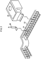
2 ist eine perspektivische Ansicht, welche das Innere eines Gehäuses der in1 gezeigten Halbleitervorrichtung veranschaulicht.2 FIG. 15 is a perspective view showing the inside of a housing of FIG1 illustrated semiconductor device illustrated. -
3 ist eine perspektivische Ansicht, welche eine Situation veranschaulicht, in der ein Anschluss an dem in1 gezeigten Gehäuse angebracht wird.3 FIG. 15 is a perspective view illustrating a situation in which a connection to the in1 shown housing is attached. -
4 ist eine Querschnittsansicht, welche eine Halbleitervorrichtung gemäß einem Vergleichsbeispiel veranschaulicht.4 FIG. 10 is a cross-sectional view illustrating a semiconductor device according to a comparative example. FIG. -
5 ist eine Querschnittsansicht, welche ein modifiziertes Beispiel der Halbleitervorrichtung der ersten Ausführungsform veranschaulicht.5 FIG. 10 is a cross-sectional view illustrating a modified example of the semiconductor device of the first embodiment. FIG. -
6 ist eine perspektivische Ansicht, welche die untere Oberfläche der Abdeckung der in5 gezeigten Halbleitervorrichtung veranschaulicht.6 FIG. 15 is a perspective view showing the lower surface of the cover of FIG5 illustrated semiconductor device illustrated. -
7 ist eine Querschnittsansicht, welche eine Halbleitervorrichtung gemäß einer zweiten Ausführungsform veranschaulicht.7 FIG. 10 is a cross-sectional view illustrating a semiconductor device according to a second embodiment. FIG.
Detaillierte Beschreibung der bevorzugten AusführungsformenDetailed Description of the Preferred Embodiments
Eine Halbleitervorrichtung gemäß den Ausführungsformen der Erfindung wird mit Bezug auf die Zeichnungen beschrieben. Die gleichen Komponenten werden durch die gleichen Symbole gekennzeichnet und die Wiederholung ihrer Beschreibung wird ausgelassen.A semiconductor device according to the embodiments of the invention will be described with reference to the drawings. The same components are represented by the same symbols and the repetition of their description is omitted.
Erste AusführungsformFirst embodiment
Ein Muttergehäuse bzw. Hauptgehäuse
Wie in
Darüber hinaus ist eine Stütze
Effekte der vorliegenden Ausführungsform werden in Bezug auf ein Vergleichsbeispiel beschrieben.
Andererseits ist gemäß der vorliegenden Ausführungsform der Kontaktteil zwischen dem Muttergehäuse
Zweite AusführungsformSecond embodiment
Darüber hinaus ist, wenn die Abdeckung
Der gleiche Effekt wird ungeachtet der Tatsache erhalten, ob die Gummidichtung
Claims (3)
Applications Claiming Priority (2)
| Application Number | Priority Date | Filing Date | Title |
|---|---|---|---|
| JP2010-115526 | 2010-05-19 | ||
| JP2010115526A JP5229271B2 (en) | 2010-05-19 | 2010-05-19 | Semiconductor device |
Publications (2)
| Publication Number | Publication Date |
|---|---|
| DE102011007228A1 DE102011007228A1 (en) | 2011-11-24 |
| DE102011007228B4 true DE102011007228B4 (en) | 2019-08-22 |
Family
ID=44900590
Family Applications (1)
| Application Number | Title | Priority Date | Filing Date |
|---|---|---|---|
| DE102011007228.4A Active DE102011007228B4 (en) | 2010-05-19 | 2011-04-12 | Semiconductor device |
Country Status (3)
| Country | Link |
|---|---|
| JP (1) | JP5229271B2 (en) |
| CN (1) | CN102254878B (en) |
| DE (1) | DE102011007228B4 (en) |
Families Citing this family (4)
| Publication number | Priority date | Publication date | Assignee | Title |
|---|---|---|---|---|
| JP5015953B2 (en) | 2005-12-23 | 2012-09-05 | スリーエム イノベイティブ プロパティズ カンパニー | Multilayer films containing thermoplastic silicone block copolymers |
| JP6848802B2 (en) | 2017-10-11 | 2021-03-24 | 三菱電機株式会社 | Semiconductor device |
| JP6861622B2 (en) * | 2017-12-19 | 2021-04-21 | 三菱電機株式会社 | Semiconductor equipment and power conversion equipment |
| EP4270469A1 (en) * | 2022-04-29 | 2023-11-01 | Infineon Technologies AG | Power semiconductor module |
Citations (8)
| Publication number | Priority date | Publication date | Assignee | Title |
|---|---|---|---|---|
| DE3308720A1 (en) | 1983-03-11 | 1984-09-13 | Siemens AG, 1000 Berlin und 8000 München | SEMICONDUCTOR COMPONENT WITH DISC-SHAPED HOUSING |
| JPS63164345A (en) | 1986-12-26 | 1988-07-07 | Nec Corp | Package for semiconductor integrated circuit |
| US5646445A (en) | 1995-07-07 | 1997-07-08 | Mitsubishi Denki Kabushiki Kaisha | Semiconductor device having electrodes embedded in an insulating case |
| JP2004103936A (en) | 2002-09-11 | 2004-04-02 | Mitsubishi Electric Corp | Power semiconductor device and manufacturing method thereof |
| US6787893B2 (en) | 2001-01-23 | 2004-09-07 | Mitsubishi Denki Kabushiki Kaisha | Semiconductor device |
| EP1494278A1 (en) | 2003-07-04 | 2005-01-05 | Siemens Aktiengesellschaft | Electronic power module with rubber seal, and corresponding manufacturing method |
| EP1768182A2 (en) | 2005-09-27 | 2007-03-28 | Semikron Elektronik GmbH & Co. KG Patentabteilung | Semiconductor power module with overcurrent protection means |
| DE102008051560A1 (en) | 2007-10-18 | 2009-04-23 | Infineon Technologies Ag | Power module, particularly power semiconductor module, has housing with multiple receiving elements and carrier element, where elastic deformable cover is arranged on carrier element |
Family Cites Families (7)
| Publication number | Priority date | Publication date | Assignee | Title |
|---|---|---|---|---|
| US4079511A (en) * | 1976-07-30 | 1978-03-21 | Amp Incorporated | Method for packaging hermetically sealed integrated circuit chips on lead frames |
| JPS6329957A (en) * | 1986-07-23 | 1988-02-08 | Seiko Epson Corp | Sealing type of semiconductor device |
| JPH02307250A (en) * | 1989-05-23 | 1990-12-20 | Mitsubishi Electric Corp | Hybrid integrated circuit package |
| CN100361317C (en) * | 2004-02-27 | 2008-01-09 | 矽品精密工业股份有限公司 | Package of possessing support piece for packing light sensitive semiconductor |
| JP4242401B2 (en) * | 2006-06-29 | 2009-03-25 | 三菱電機株式会社 | Semiconductor device |
| CN101101880A (en) * | 2006-07-03 | 2008-01-09 | 矽品精密工业股份有限公司 | Heat-radiation type package structure and its method for making |
| JP4858336B2 (en) * | 2007-07-10 | 2012-01-18 | 三菱電機株式会社 | Power semiconductor device |
-
2010
- 2010-05-19 JP JP2010115526A patent/JP5229271B2/en active Active
-
2011
- 2011-04-12 DE DE102011007228.4A patent/DE102011007228B4/en active Active
- 2011-04-15 CN CN201110104259.7A patent/CN102254878B/en active Active
Patent Citations (8)
| Publication number | Priority date | Publication date | Assignee | Title |
|---|---|---|---|---|
| DE3308720A1 (en) | 1983-03-11 | 1984-09-13 | Siemens AG, 1000 Berlin und 8000 München | SEMICONDUCTOR COMPONENT WITH DISC-SHAPED HOUSING |
| JPS63164345A (en) | 1986-12-26 | 1988-07-07 | Nec Corp | Package for semiconductor integrated circuit |
| US5646445A (en) | 1995-07-07 | 1997-07-08 | Mitsubishi Denki Kabushiki Kaisha | Semiconductor device having electrodes embedded in an insulating case |
| US6787893B2 (en) | 2001-01-23 | 2004-09-07 | Mitsubishi Denki Kabushiki Kaisha | Semiconductor device |
| JP2004103936A (en) | 2002-09-11 | 2004-04-02 | Mitsubishi Electric Corp | Power semiconductor device and manufacturing method thereof |
| EP1494278A1 (en) | 2003-07-04 | 2005-01-05 | Siemens Aktiengesellschaft | Electronic power module with rubber seal, and corresponding manufacturing method |
| EP1768182A2 (en) | 2005-09-27 | 2007-03-28 | Semikron Elektronik GmbH & Co. KG Patentabteilung | Semiconductor power module with overcurrent protection means |
| DE102008051560A1 (en) | 2007-10-18 | 2009-04-23 | Infineon Technologies Ag | Power module, particularly power semiconductor module, has housing with multiple receiving elements and carrier element, where elastic deformable cover is arranged on carrier element |
Non-Patent Citations (1)
| Title |
|---|
| JP S63- 164 345 A (Maschinenübersetzung), AIPN [online] JPO [abgerufen am 06.03.2019] * |
Also Published As
| Publication number | Publication date |
|---|---|
| CN102254878A (en) | 2011-11-23 |
| CN102254878B (en) | 2015-01-14 |
| DE102011007228A1 (en) | 2011-11-24 |
| JP2011243798A (en) | 2011-12-01 |
| JP5229271B2 (en) | 2013-07-03 |
Similar Documents
| Publication | Publication Date | Title |
|---|---|---|
| DE102011077543B4 (en) | Semiconductor device | |
| DE102004010658B4 (en) | junction box | |
| DE102011075365B4 (en) | Semiconductor device and manufacturing method thereof | |
| DE102009042399B4 (en) | Power semiconductor device and manufacturing method therefor | |
| DE102012208361A1 (en) | INTEGRATED PRESSURE SENSOR | |
| DE112011103926T5 (en) | Semiconductor device and method of manufacturing a semiconductor device | |
| DE102005050327A1 (en) | Antenna mounted on a vehicle | |
| DE19649798A1 (en) | Power semiconductor module | |
| EP2583318A1 (en) | Surface-mountable optoelectronic component and method for producing a surface-mountable optoelectronic component | |
| DE10217101A1 (en) | Electronic vehicle control unit | |
| DE102011007228B4 (en) | Semiconductor device | |
| DE2733724A1 (en) | SEMICONDUCTOR COMPONENT WITH PLASTIC ENCAPSULATION | |
| DE102014104856A1 (en) | Explosion-proof power semiconductor module | |
| DE7929603U1 (en) | Electrical device, preferably relays for motor vehicles | |
| DE102018212828A1 (en) | Semiconductor device | |
| DE102014115099A1 (en) | Electronic module with electrically insulating structure with low modulus material | |
| DE102014200015B4 (en) | Waterproof main connection | |
| DE10161936A1 (en) | Electronic control unit | |
| EP2227929B1 (en) | Electronic unit with a housing | |
| DE102008045721B4 (en) | Semiconductor device | |
| EP1959494B1 (en) | Power semiconductor module | |
| DE102007032074A1 (en) | Electronic components encapsulating electronic housing therein | |
| DE102009013782A1 (en) | Semiconductor packaging construction with protective strip | |
| DE102013207552A1 (en) | Semiconductor module | |
| DE102017207117A1 (en) | A semiconductor device |
Legal Events
| Date | Code | Title | Description |
|---|---|---|---|
| R012 | Request for examination validly filed | ||
| R016 | Response to examination communication | ||
| R084 | Declaration of willingness to licence | ||
| R018 | Grant decision by examination section/examining division | ||
| R020 | Patent grant now final |