EP1768182A2 - Semiconductor power module with overcurrent protection means - Google Patents
Semiconductor power module with overcurrent protection means Download PDFInfo
- Publication number
- EP1768182A2 EP1768182A2 EP06020214A EP06020214A EP1768182A2 EP 1768182 A2 EP1768182 A2 EP 1768182A2 EP 06020214 A EP06020214 A EP 06020214A EP 06020214 A EP06020214 A EP 06020214A EP 1768182 A2 EP1768182 A2 EP 1768182A2
- Authority
- EP
- European Patent Office
- Prior art keywords
- power semiconductor
- semiconductor module
- frame
- connection
- section
- Prior art date
- Legal status (The legal status is an assumption and is not a legal conclusion. Google has not performed a legal analysis and makes no representation as to the accuracy of the status listed.)
- Granted
Links
Images

Classifications
-
- H—ELECTRICITY
- H01—ELECTRIC ELEMENTS
- H01L—SEMICONDUCTOR DEVICES NOT COVERED BY CLASS H10
- H01L23/00—Details of semiconductor or other solid state devices
- H01L23/34—Arrangements for cooling, heating, ventilating or temperature compensation ; Temperature sensing arrangements
- H01L23/36—Selection of materials, or shaping, to facilitate cooling or heating, e.g. heatsinks
- H01L23/373—Cooling facilitated by selection of materials for the device or materials for thermal expansion adaptation, e.g. carbon
- H01L23/3735—Laminates or multilayers, e.g. direct bond copper ceramic substrates
-
- H—ELECTRICITY
- H01—ELECTRIC ELEMENTS
- H01L—SEMICONDUCTOR DEVICES NOT COVERED BY CLASS H10
- H01L23/00—Details of semiconductor or other solid state devices
- H01L23/58—Structural electrical arrangements for semiconductor devices not otherwise provided for, e.g. in combination with batteries
- H01L23/62—Protection against overvoltage, e.g. fuses, shunts
-
- H—ELECTRICITY
- H01—ELECTRIC ELEMENTS
- H01L—SEMICONDUCTOR DEVICES NOT COVERED BY CLASS H10
- H01L25/00—Assemblies consisting of a plurality of individual semiconductor or other solid state devices ; Multistep manufacturing processes thereof
- H01L25/03—Assemblies consisting of a plurality of individual semiconductor or other solid state devices ; Multistep manufacturing processes thereof all the devices being of a type provided for in the same subgroup of groups H01L27/00 - H01L33/00, or in a single subclass of H10K, H10N, e.g. assemblies of rectifier diodes
- H01L25/04—Assemblies consisting of a plurality of individual semiconductor or other solid state devices ; Multistep manufacturing processes thereof all the devices being of a type provided for in the same subgroup of groups H01L27/00 - H01L33/00, or in a single subclass of H10K, H10N, e.g. assemblies of rectifier diodes the devices not having separate containers
- H01L25/07—Assemblies consisting of a plurality of individual semiconductor or other solid state devices ; Multistep manufacturing processes thereof all the devices being of a type provided for in the same subgroup of groups H01L27/00 - H01L33/00, or in a single subclass of H10K, H10N, e.g. assemblies of rectifier diodes the devices not having separate containers the devices being of a type provided for in group H01L29/00
- H01L25/072—Assemblies consisting of a plurality of individual semiconductor or other solid state devices ; Multistep manufacturing processes thereof all the devices being of a type provided for in the same subgroup of groups H01L27/00 - H01L33/00, or in a single subclass of H10K, H10N, e.g. assemblies of rectifier diodes the devices not having separate containers the devices being of a type provided for in group H01L29/00 the devices being arranged next to each other
-
- H—ELECTRICITY
- H01—ELECTRIC ELEMENTS
- H01L—SEMICONDUCTOR DEVICES NOT COVERED BY CLASS H10
- H01L2224/00—Indexing scheme for arrangements for connecting or disconnecting semiconductor or solid-state bodies and methods related thereto as covered by H01L24/00
- H01L2224/01—Means for bonding being attached to, or being formed on, the surface to be connected, e.g. chip-to-package, die-attach, "first-level" interconnects; Manufacturing methods related thereto
- H01L2224/42—Wire connectors; Manufacturing methods related thereto
- H01L2224/44—Structure, shape, material or disposition of the wire connectors prior to the connecting process
- H01L2224/45—Structure, shape, material or disposition of the wire connectors prior to the connecting process of an individual wire connector
- H01L2224/45001—Core members of the connector
- H01L2224/4501—Shape
- H01L2224/45012—Cross-sectional shape
- H01L2224/45015—Cross-sectional shape being circular
-
- H—ELECTRICITY
- H01—ELECTRIC ELEMENTS
- H01L—SEMICONDUCTOR DEVICES NOT COVERED BY CLASS H10
- H01L2224/00—Indexing scheme for arrangements for connecting or disconnecting semiconductor or solid-state bodies and methods related thereto as covered by H01L24/00
- H01L2224/01—Means for bonding being attached to, or being formed on, the surface to be connected, e.g. chip-to-package, die-attach, "first-level" interconnects; Manufacturing methods related thereto
- H01L2224/42—Wire connectors; Manufacturing methods related thereto
- H01L2224/47—Structure, shape, material or disposition of the wire connectors after the connecting process
- H01L2224/48—Structure, shape, material or disposition of the wire connectors after the connecting process of an individual wire connector
- H01L2224/484—Connecting portions
- H01L2224/4846—Connecting portions with multiple bonds on the same bonding area
-
- H—ELECTRICITY
- H01—ELECTRIC ELEMENTS
- H01L—SEMICONDUCTOR DEVICES NOT COVERED BY CLASS H10
- H01L2224/00—Indexing scheme for arrangements for connecting or disconnecting semiconductor or solid-state bodies and methods related thereto as covered by H01L24/00
- H01L2224/01—Means for bonding being attached to, or being formed on, the surface to be connected, e.g. chip-to-package, die-attach, "first-level" interconnects; Manufacturing methods related thereto
- H01L2224/42—Wire connectors; Manufacturing methods related thereto
- H01L2224/47—Structure, shape, material or disposition of the wire connectors after the connecting process
- H01L2224/48—Structure, shape, material or disposition of the wire connectors after the connecting process of an individual wire connector
- H01L2224/484—Connecting portions
- H01L2224/4847—Connecting portions the connecting portion on the bonding area of the semiconductor or solid-state body being a wedge bond
- H01L2224/48472—Connecting portions the connecting portion on the bonding area of the semiconductor or solid-state body being a wedge bond the other connecting portion not on the bonding area also being a wedge bond, i.e. wedge-to-wedge
-
- H—ELECTRICITY
- H01—ELECTRIC ELEMENTS
- H01L—SEMICONDUCTOR DEVICES NOT COVERED BY CLASS H10
- H01L2224/00—Indexing scheme for arrangements for connecting or disconnecting semiconductor or solid-state bodies and methods related thereto as covered by H01L24/00
- H01L2224/73—Means for bonding being of different types provided for in two or more of groups H01L2224/10, H01L2224/18, H01L2224/26, H01L2224/34, H01L2224/42, H01L2224/50, H01L2224/63, H01L2224/71
- H01L2224/732—Location after the connecting process
- H01L2224/73251—Location after the connecting process on different surfaces
- H01L2224/73265—Layer and wire connectors
-
- H—ELECTRICITY
- H01—ELECTRIC ELEMENTS
- H01L—SEMICONDUCTOR DEVICES NOT COVERED BY CLASS H10
- H01L2224/00—Indexing scheme for arrangements for connecting or disconnecting semiconductor or solid-state bodies and methods related thereto as covered by H01L24/00
- H01L2224/80—Methods for connecting semiconductor or other solid state bodies using means for bonding being attached to, or being formed on, the surface to be connected
- H01L2224/85—Methods for connecting semiconductor or other solid state bodies using means for bonding being attached to, or being formed on, the surface to be connected using a wire connector
- H01L2224/85909—Post-treatment of the connector or wire bonding area
- H01L2224/8592—Applying permanent coating, e.g. protective coating
-
- H—ELECTRICITY
- H01—ELECTRIC ELEMENTS
- H01L—SEMICONDUCTOR DEVICES NOT COVERED BY CLASS H10
- H01L24/00—Arrangements for connecting or disconnecting semiconductor or solid-state bodies; Methods or apparatus related thereto
- H01L24/01—Means for bonding being attached to, or being formed on, the surface to be connected, e.g. chip-to-package, die-attach, "first-level" interconnects; Manufacturing methods related thereto
- H01L24/42—Wire connectors; Manufacturing methods related thereto
- H01L24/47—Structure, shape, material or disposition of the wire connectors after the connecting process
- H01L24/48—Structure, shape, material or disposition of the wire connectors after the connecting process of an individual wire connector
-
- H—ELECTRICITY
- H01—ELECTRIC ELEMENTS
- H01L—SEMICONDUCTOR DEVICES NOT COVERED BY CLASS H10
- H01L2924/00—Indexing scheme for arrangements or methods for connecting or disconnecting semiconductor or solid-state bodies as covered by H01L24/00
- H01L2924/0001—Technical content checked by a classifier
- H01L2924/00014—Technical content checked by a classifier the subject-matter covered by the group, the symbol of which is combined with the symbol of this group, being disclosed without further technical details
-
- H—ELECTRICITY
- H01—ELECTRIC ELEMENTS
- H01L—SEMICONDUCTOR DEVICES NOT COVERED BY CLASS H10
- H01L2924/00—Indexing scheme for arrangements or methods for connecting or disconnecting semiconductor or solid-state bodies as covered by H01L24/00
- H01L2924/01—Chemical elements
- H01L2924/0102—Calcium [Ca]
-
- H—ELECTRICITY
- H01—ELECTRIC ELEMENTS
- H01L—SEMICONDUCTOR DEVICES NOT COVERED BY CLASS H10
- H01L2924/00—Indexing scheme for arrangements or methods for connecting or disconnecting semiconductor or solid-state bodies as covered by H01L24/00
- H01L2924/19—Details of hybrid assemblies other than the semiconductor or other solid state devices to be connected
- H01L2924/191—Disposition
- H01L2924/19101—Disposition of discrete passive components
- H01L2924/19105—Disposition of discrete passive components in a side-by-side arrangement on a common die mounting substrate
-
- H—ELECTRICITY
- H01—ELECTRIC ELEMENTS
- H01L—SEMICONDUCTOR DEVICES NOT COVERED BY CLASS H10
- H01L2924/00—Indexing scheme for arrangements or methods for connecting or disconnecting semiconductor or solid-state bodies as covered by H01L24/00
- H01L2924/19—Details of hybrid assemblies other than the semiconductor or other solid state devices to be connected
- H01L2924/191—Disposition
- H01L2924/19101—Disposition of discrete passive components
- H01L2924/19107—Disposition of discrete passive components off-chip wires
-
- H—ELECTRICITY
- H01—ELECTRIC ELEMENTS
- H01L—SEMICONDUCTOR DEVICES NOT COVERED BY CLASS H10
- H01L2924/00—Indexing scheme for arrangements or methods for connecting or disconnecting semiconductor or solid-state bodies as covered by H01L24/00
- H01L2924/30—Technical effects
- H01L2924/301—Electrical effects
- H01L2924/30107—Inductance
Definitions
- the invention describes a power semiconductor module consisting of a housing, preferably with a base plate for mounting on a heat sink and at least one electrically insulating substrate arranged therein.
- a power semiconductor module consisting of a housing, preferably with a base plate for mounting on a heat sink and at least one electrically insulating substrate arranged therein.
- This in turn consists of an insulating body with a plurality of mutually insulated metallic interconnect tracks located thereon and power semiconductor components located thereon and connected in a circuitally correct manner to these interconnect tracks.
- the power semiconductor module has connection elements for external load and auxiliary contacts and also connection elements for connections in the interior of the power semiconductor module.
- Power semiconductor modules which are the starting point of this invention are known by way of example from US Pat DE 103 16 355 B3 , This document discloses a power semiconductor module in the form of a half-bridge circuit arrangement with a first and a second circuit breaker. Each of these power switches is designed as a parallel circuit of power transistors, each having an associated freewheeling diode. Depending on a first and a second power transistor with associated power diode in this case is arranged on a separate substrate.
- the substrates of such power semiconductor modules are formed as insulating substrates consisting of an insulating body as a carrier material and for electrical insulation against a base plate or a heat sink.
- This Isolierstoff Archives consists of the prior art from an industrial ceramics exemplified alumina or aluminum nitrite.
- On this insulating body on the interior of the power semiconductor module facing the first main surface, there is a plurality of mutually electrically insulated metallic interconnect tracks. In turn, the power semiconductor components are arranged on these.
- the insulating material body also has on its second main surface facing away from the interior of the power semiconductor module a metallic layer of the same material and the same thickness as that of the connecting tracks on the first main surface.
- this layer is not structured in itself, since it serves as an example of the solder joint to a base plate.
- the connecting tracks and the metallic layer of the second main surface preferably consists of copper applied by the DCB (direct copper bonding) method, the copper in this case having a typical thickness of less than 1 mm.
- the mentioned power semiconductor modules according to the prior art have load connection elements for the two DC connections and for the at least one AC connection.
- the load connection elements connect external contacts with associated connection tracks on the substrate.
- the object of the invention is to further develop a power semiconductor module with a protective device arranged in the interior of the power semiconductor module in order to prevent an explosion-like destruction of the power semiconductor module due to excessively high currents.
- the protective device against excessively high currents in the interior of the power semiconductor module will be referred to as a safety device in the following.
- the inventive concept is based on a power semiconductor module, preferably with a base plate for mounting on a heat sink.
- This power semiconductor module has at least the following components: a housing, connecting elements for load and auxiliary terminals, at least one substrate with connecting tracks and at least one power semiconductor component.
- connection elements for load connections lead out of the housing and serve for the electrical connection of the power semiconductor components arranged inside the housing.
- the base plate or a heat sink electrically insulating formed substrate in turn consists of a Isolierstoff emotions, preferably an industrial ceramic, and thereon, on which the base plate or the heat sink facing away from the first main surface befindlich, a plurality of mutually electrically insulated metallic interconnect tracks.
- Power semiconductor components are arranged on these connection tracks and connected in accordance with the circuit by means of first connecting elements with a first line cross-section.
- these first connecting elements are designed as bond connections with a plurality of individual bonding wires.
- Such a bond connection has a first line cross-section, which is formed by the sum of the cross-sectional areas of all bond wires of the bond connection.
- the power semiconductor module has in its interior at least one securing device, wherein this securing device consists of a second connecting element with a second, compared to the first smaller, line cross-section.
- the securing device is arranged between two connecting tracks and / or between a connecting track and a load connecting element. Furthermore, this second connecting element is completely enveloped in a subsection by an explosion protection agent.
- This explosion protection agent allows a controlled formation of an arc, without it in this explosion protection means leads to a very rapid pressure increase, which ends in an explosion.
- Fig. 1 shows a circuit topology of a power semiconductor module according to the prior art.
- FIG. 2 shows a circuit topology of a power semiconductor module according to the invention.
- FIG 3 shows an embodiment of a power semiconductor module according to the invention.
- FIG. 1 shows a circuit topology of a power semiconductor module (1) according to the prior art. Shown here is a half-bridge circuit as it is the basic building block of many power electronic circuit topologies. Here, a first, upper, circuit breaker (70) with a second lower power switch (72) connected in series. The first power switch (70) is connected to the positive terminal (42) of a DC intermediate circuit. The second power switch (72) is connected to the negative terminal (46) of the DC link. The center tap of the circuit forms the AC output (44) of the half-bridge circuit.
- the power switches (70, 72) are designed as an arrangement of at least one power transistor (70a, 72a) and at least one power diode (70b, 72b) connected in antiparallel with respect thereto.
- FIG. 2 shows a circuit topology of a power semiconductor module (1) according to the invention.
- the illustrated circuit topology is also the half-bridge circuit. Nevertheless, the inventive idea can be used in any other circuit topology.
- the invention based on this circuit power semiconductor module (1) is further developed by at least one, here three, safety devices (6 a / b / c) are integrated into the circuit.
- An advantageous embodiment here is the arrangement of a securing device (6b) between the center tap and the AC power connection (44).
- a further advantageous embodiment arranges for each one fuse (6a, 6c) between the respective DC connection (42, 46) and the associated circuit breaker (70, 72).
- the arrangement of three safety devices (6 a / b / c) within a power semiconductor module (1) is the most expensive, but at the same time safest embodiment of the invention.
- the arrangement of only one safety device (6 a / b / c) can not protect against all possible failure scenarios, but forms a meaningful compromise of effort and benefits.
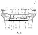
- FIG. 3 shows a power semiconductor module (1) according to the invention.
- This has a base plate (2), on which the housing (3) and a substrate (5) are arranged.
- the substrate (5) consists of an insulating body (54) and metallic laminations, which are arranged on both major surfaces.
- the base plate (2) facing metallic lamination (53) is flat and not structured in itself. By means of a solder joint between this lamination (53) and the base plate (2) they are fixed to each other.
- the lining facing the power semiconductor module inside lamination is structured in itself and thus forms the connecting tracks (52) of the substrate (5).
- connection elements shown here a DC connection (42) of positive polarity and an AC connection (44) are formed by metal moldings, which are soldered at one end with the associated connection web (52) and at its other end have a recess for screw connection.
- the power semiconductor components (70, 72), shown here a power diode (70b), are arranged on these connection tracks (52).
- the electrical connection elements form the power (42, 44) and not explicitly shown auxiliary terminals.
- the circuit-compatible connection of the power semiconductor components (70, 72), here the power diode (70b) according to the circuit topology of FIG. 2 with the connecting tracks (52) is formed as a bond connection (40).
- this bonding ten individual bonding wires with a diameter of 300 microns, whereby a first line cross section of the connection results for this power semiconductor device of about 0.71 mm 2.
- the first embodiment has a bond connection (60) between the conductor track (52) of the positive terminal and the conductor track (52) of the power diode (70b), which is arranged thereon on the cathode side.
- This bond connection (60) is formed by means of 5 bonding wires with a diameter of 300 ⁇ m each.
- the configuration of the bond connections to the power semiconductor components is determined by further variables, such as, for example, the current distribution on the power semiconductor component. Therefore, these compounds are typically formed with a significantly larger cross-section than would be necessary for the carrying capacity of a surge current.
- the bonding wires forming this second connection element (60) are surrounded by the silicon oxide (62) as explosion protection means apart from their respective contact surface with the associated conductor track (52).
- This silicon dioxide (62) advantageously has a particle size of between 50 ⁇ m and 2 mm.
- the silica is here as a pure substance (62a) or as a substance mixture (62b) with a minimum concentration of silicon oxide of 90 out of 100.
- a binder is added to the silicon oxide (62b).
- a covering of the silicon oxide (62b) is not absolutely necessary because it encloses the bonding wires (60) in bonded form and is thus fixed in its position in the power semiconductor module (1).
- the bonding wires (60) with the explosion protection means (62) are surrounded by a frame-like arrangement (32), which is designed here as a housing part and is arranged on the substrate (5) by means of an adhesive connection.
- the housing (3) has on its upper side a suitable recess (30) for filling the power semiconductor module with the explosion protection means (62).
- the second illustrated embodiment shows a frame-like limiting device (64), preferably made of a plastic material, which is adhesively bonded to the substrate (5). Inside this limiting device (64), the bond connection and the explosion protection means (60) are arranged. If this does not have the addition of a binder, in this case a closure means (66), for example an epoxy resin, is provided in order to fix the explosion protection means (60a) in the intended position.
- a closure means for example an epoxy resin
Abstract
Description
Die Erfindung beschreibt ein Leistungshalbleitermodul bestehend aus einem Gehäuse vorzugsweise mit einer Grundplatte zur Montage auf einem Kühlkörper und mindestens einem darin angeordneten elektrisch isolierenden Substrat. Dieses besteht seinerseits aus einem Isolierstoffkörper mit einer Mehrzahl darauf befindlicher gegeneinander isolierter metallischer Verbindungsbahnen und hierauf befindlichen und mit diesen Verbindungsbahnen schaltungsgerecht verbundenen Leistungshalbleiterbauelementen. Weiterhin weist das Leistungshalbleitermodul Anschlusselemente für externe Last- und Hilfskontakte und auch Verbindungselemente für Verbindungen im Inneren des Leistungshalbleitermoduls auf.The invention describes a power semiconductor module consisting of a housing, preferably with a base plate for mounting on a heat sink and at least one electrically insulating substrate arranged therein. This in turn consists of an insulating body with a plurality of mutually insulated metallic interconnect tracks located thereon and power semiconductor components located thereon and connected in a circuitally correct manner to these interconnect tracks. Furthermore, the power semiconductor module has connection elements for external load and auxiliary contacts and also connection elements for connections in the interior of the power semiconductor module.
Leistungshalbleitermodule, die Ausgangspunkt dieser Erfindung sind, sind beispielhaft bekannt aus der
Gemäß der als Stand der Technik genannten Druckschrift sind die Substrate derartiger Leistungshalbleitermodule ausgebildet als isolierende Substrate bestehend aus einem Isolierstoffkörper als Trägermaterial und zur elektrischen Isolierung gegen eine Grundplatte oder einen Kühlkörper. Dieser Isolierstoffkörper besteht nach dem Stand der Technik aus einer Industriekeramik beispielhaft Aluminiumoxid oder Aluminiumnitrit. Auf diesem lsolierstoffkörper, auf dessen dem Inneren des Leistungshalbleitermoduls zugewandten ersten Hauptfläche, befindet sich eine Mehrzahl von gegeneinander elektrisch isolierten metallischen Verbindungsbahnen. Auf diesen wiederum sind die Leistungshalbleiterbauelemente angeordnet.According to the publication cited as prior art, the substrates of such power semiconductor modules are formed as insulating substrates consisting of an insulating body as a carrier material and for electrical insulation against a base plate or a heat sink. This Isolierstoffkörper consists of the prior art from an industrial ceramics exemplified alumina or aluminum nitrite. On this insulating body, on the interior of the power semiconductor module facing the first main surface, there is a plurality of mutually electrically insulated metallic interconnect tracks. In turn, the power semiconductor components are arranged on these.
Meist weist der Isolierstoffkörper auf seiner dem Inneren des Leistungshalbleitermoduls abgewandten zweiten Hauptfläche ebenfalls eine metallische Schicht gleichen Materials und gleicher Dicke wie diejenige der Verbindungsbahnen auf der ersten Hauptfläche auf. In der Regel ist diese Schicht allerdings nicht in sich strukturiert, da sie beispielhaft der Lötverbindung zu einer Grundplatte dient. Die Verbindungsbahnen sowie die metallische Schicht der zweiten Hauptfläche besteht vorzugsweise aus nach dem DCB (direct copper bonding) Verfahren aufgebrachten Kupfer, wobei das Kupfer hierbei eine typische Dicke von weniger als 1 mm aufweist.In most cases, the insulating material body also has on its second main surface facing away from the interior of the power semiconductor module a metallic layer of the same material and the same thickness as that of the connecting tracks on the first main surface. In general, however, this layer is not structured in itself, since it serves as an example of the solder joint to a base plate. The connecting tracks and the metallic layer of the second main surface preferably consists of copper applied by the DCB (direct copper bonding) method, the copper in this case having a typical thickness of less than 1 mm.
Weiterhin weisen die genannten Leistungshalbleitermodule nach dem Stand der Technik Lastanschlusselemente für die beiden Gleichstromanschlüsse und für den mindestens einen Wechselstromanschluss auf. Die Lastanschlusselemente verbinden äußere Kontaktierungen mit zugeordneten Verbindungsbahnen auf dem Substrat.Furthermore, the mentioned power semiconductor modules according to the prior art have load connection elements for the two DC connections and for the at least one AC connection. The load connection elements connect external contacts with associated connection tracks on the substrate.
Zur Inneren Isolation sind Leistungshalbleitermodule nach dem Stand der Technik bis oberhalb der Verbindungselemente mit einer Vergussmasse mit hoher Dielektrizitätskonstante vergossen.For internal isolation, power semiconductor modules according to the prior art are potted with a potting compound of high dielectric constant above the connecting elements.
Moderne Leistungshalbleiterbauelemente, besonders Leistungstransistoren, weisen im Zuge des technologischen Fortschritts eine stetig wachsende Stromdichte auf. Typische Verbindungselemente zwischen den Leistungshalbleiterbauelementen und den Verbindungsbahnen sind Bondverbindungen und hier speziell Drahtbondverbindungen. Nach dem Stand der Technik werden verschiedene Fehlerszenarien beim Einsatz von Leistungshalbleitermodulen durch geeignete Sensoren im oder in der Beschaltung des Leistungshalbleitermoduls erfasst und durch die Ansteuerelektronik Gegenmaßnahmen, wie beispielsweise das Abschalten der Leistungsschalter, eingeleitet. Es gibt allerdings auch Fehlerszenarien, die hierdurch nicht oder nicht vollständig erfasst werden. In diesen Fällen entsteht im Inneren des Leistungshalbleitermoduls ein kurzzeitig fließender Überstrom, der die Bonddrähte überlastet. Dieser Überstrom führt zum Schmetzenmindestens eines Bonddrahtes, wobei durch die vorhandenen Induktivitäten der Stromfluss in Form eines Lichtbogens aufrecht erhalten bleibt. Dies führt bei Leistungshalbleitermodulen mit Vergussmasse auf Grund der in dem kurzen Zeitintervall fehlenden Kompressibilität dieser Vergussmasse und des sich somit schnell aufbauenden inneren Drucks häufig zu einer Explosion des Leistungshalbleitermoduls.Modern power semiconductor devices, especially power transistors, have a steadily increasing current density as technology advances. Typical connecting elements between the power semiconductor components and the connecting tracks are bonding connections and here especially wire bonds. According to the prior art, various fault scenarios when using power semiconductor modules are detected by suitable sensors in or in the circuit of the power semiconductor module and by the control electronics countermeasures, such as switching off the circuit breaker initiated. There are, however also error scenarios that are not or not completely covered. In these cases, a short-term overcurrent occurs in the interior of the power semiconductor module, which overloads the bonding wires. This overcurrent leads to the melting of at least one bonding wire, whereby the current flow in the form of an arc is maintained by the existing inductances. This leads in power semiconductor modules with potting compound due to the lack of compressibility in the short time interval this potting compound and thus quickly building up internal pressure to an explosion of the power semiconductor module.
Der Erfindung liegt die Aufgabe zugrunde ein Leistungshalbleitermodul weiterzubilden mit einer im Inneren des Leistungshalbleitermoduls angeordneten Schutzeinrichtung um eine durch zu hohe Ströme bedingte explosionsartige Zerstörung des Leistungshalbleitermoduls zu verhindern.The object of the invention is to further develop a power semiconductor module with a protective device arranged in the interior of the power semiconductor module in order to prevent an explosion-like destruction of the power semiconductor module due to excessively high currents.
Die Schutzeinrichtung gegen zu hohe Ströme im Inneren des Leistungshalbleitermoduls soll im Folgenden vereinfachend als Sicherungseinrichtung bezeichnet werden.The protective device against excessively high currents in the interior of the power semiconductor module will be referred to as a safety device in the following.
Die Aufgabe wird erfindungsgemäß gelöst, durch die Maßnahmen der Merkmale des Anspruchs 1. Bevorzugte Ausführungsformen sind in den Unteransprüchen beschrieben.The object is achieved by the measures of the features of
Der erfinderische Gedanke geht aus von einem Leistungshalbleitermodul vorzugsweise mit einer Grundplatte zur Montage auf einem Kühlkörper. Dieses Leistungshalbleitermodul weist mindestens folgende Komponenten auf: ein Gehäuse, Anschlusselemente für Last- und Hilfsanschlüsse, mindestens ein Substrat mit Verbindungsbahnen und mindestens eine Leistungshalbleiterbauelement.The inventive concept is based on a power semiconductor module, preferably with a base plate for mounting on a heat sink. This power semiconductor module has at least the following components: a housing, connecting elements for load and auxiliary terminals, at least one substrate with connecting tracks and at least one power semiconductor component.
Die Anschlusselemente für Lastanschlüsse führen aus dem Gehäuse heraus und dienen der elektrischen Verbindung der im Gehäuseinneren angeordneten Leistungshalbleiterbauelemente. Das zur Grundplatte oder einem Kühlkörper elektrisch isolierend ausgebildeten Substrat besteht seinerseits aus einem Isolierstoffkörper, vorzugsweise einer Industriekeramik, und hierauf, auf dessen der Grundplatte oder dem Kühlkörper abgewandten ersten Hauptfläche befindlich, einer Mehrzahl von gegeneinander elektrisch isolierten metallischen Verbindungsbahnen. Auf diesen Verbindungsbahnen sind Leistungshalbleiterbauelemente angeordnet und schaltungsgerecht mittels ersten Verbindungselementen mit einem ersten Leitungsquerschnitt verbunden. Vorzugsweise sind diese ersten Verbindungselementen als Bondverbindungen mit einer Mehrzahl einzelnen Bonddrähte ausgestaltet. Eine derartige Bondverbindung weist einen ersten Leitungsquerschnitt auf, der gebildet wird durch die Summe der Querschnittsflächen aller Bonddrähte der Bondverbindung.The connection elements for load connections lead out of the housing and serve for the electrical connection of the power semiconductor components arranged inside the housing. The base plate or a heat sink electrically insulating formed substrate in turn consists of a Isolierstoffkörper, preferably an industrial ceramic, and thereon, on which the base plate or the heat sink facing away from the first main surface befindlich, a plurality of mutually electrically insulated metallic interconnect tracks. Power semiconductor components are arranged on these connection tracks and connected in accordance with the circuit by means of first connecting elements with a first line cross-section. Preferably, these first connecting elements are designed as bond connections with a plurality of individual bonding wires. Such a bond connection has a first line cross-section, which is formed by the sum of the cross-sectional areas of all bond wires of the bond connection.
Das Leistungshalbleitermodul weist in seinem Inneren mindestens eine Sicherungseinrichtung auf, wobei diese Sicherungseinrichtung aus einem zweiten Verbindungselement mit einem zweiten, gegenüber dem ersten geringern, Leitungsquerschnitt besteht. Die Sicherungseinrichtung ist zwischen zwei Verbindungsbahnen und / oder zwischen einer Verbindungsbahn und einem Lastanschlusselement angeordnet. Weiterhin ist dieses zweite Verbindungselement in einem Teilabschnitt vollständig von einem Explosionsschutzmittel umhüllt. Dieses Explosionsschutzmittel erlaubt eine kontrollierte Ausbildung eines Lichtbogens, ohne dass es hierbei in diesem Explosionsschutzmittel zu einem sehr schnellen Druckanstieg führt, der in einer Explosion endet.The power semiconductor module has in its interior at least one securing device, wherein this securing device consists of a second connecting element with a second, compared to the first smaller, line cross-section. The securing device is arranged between two connecting tracks and / or between a connecting track and a load connecting element. Furthermore, this second connecting element is completely enveloped in a subsection by an explosion protection agent. This explosion protection agent allows a controlled formation of an arc, without it in this explosion protection means leads to a very rapid pressure increase, which ends in an explosion.
Die erfinderische Lösung wird an Hand der Fig. 1 bis 3 weiter erläutert.The inventive solution is further explained with reference to FIGS. 1 to 3.
Fig. 1 zeigt eine Schaltungstopologie eines Leistungshalbleitermoduls nach dem Stand der Technik.Fig. 1 shows a circuit topology of a power semiconductor module according to the prior art.
Fig. 2 zeigt eine Schaltungstopologie eines erfindungsgemäßen Leistungshalbleitermoduls.2 shows a circuit topology of a power semiconductor module according to the invention.
Fig. 3 zeigt eine Ausgestaltung eines erfindungsgemäßen Leistungshalbleitermoduls.3 shows an embodiment of a power semiconductor module according to the invention.
Fig. 1 zeigt eine Schaltungstopologie eines Leistungshalbleitermoduls (1) nach dem Stand der Technik. Dargestellt ist hier eine Halbbrückenschaltung wie sie Grundbaustein vieler leistungselektronischer Schaltungstopologien ist. Hierbei ist ein erster, oberer, Leistungsschalter (70) mit einem zweiten unteren Leistungsschalter (72) in Reihe geschalten. Der erste Leistungsschalter (70) ist mit dem positiven Anschluss (42) eines Gleichstromzwischenkreises verbunden. Der zweite Leistungsschalter (72) ist mit dem negativen Anschluss (46) des Gleichstromzwischenkreises verbunden. Der Mittelabgriff der Schaltung bildet den Wechselstromausgang (44) der Halbbrückenschaltung.1 shows a circuit topology of a power semiconductor module (1) according to the prior art. Shown here is a half-bridge circuit as it is the basic building block of many power electronic circuit topologies. Here, a first, upper, circuit breaker (70) with a second lower power switch (72) connected in series. The first power switch (70) is connected to the positive terminal (42) of a DC intermediate circuit. The second power switch (72) is connected to the negative terminal (46) of the DC link. The center tap of the circuit forms the AC output (44) of the half-bridge circuit.
Die Leistungsschalter (70,72) sind ausgebildet als eine Anordnung von mindestens einem Leistungstransistor (70a, 72a) und mindestens einer hierzu antiparallel geschalteten Leistungsdiode (70b, 72b).The power switches (70, 72) are designed as an arrangement of at least one power transistor (70a, 72a) and at least one power diode (70b, 72b) connected in antiparallel with respect thereto.
Fig. 2 zeigt eine Schaltungstopologie eines erfindungsgemäßen Leistungshalbleitermoduls (1). Die dargestellte Schaltungstopologie ist ebenfalls die Halbbrückenschaltung. Gleichwohl ist der erfinderische Gedanke in jeglicher andern Schaltungstopologie einsetzbar. Erfindungsgemäß ist das auf dieser Schaltung basierende Leistungshalbleitermodul (1) weitergebildet, indem mindestens eine, hier drei, Sicherungseinrichtungen (6 a/b/c) in die Schaltung eingebunden sind.2 shows a circuit topology of a power semiconductor module (1) according to the invention. The illustrated circuit topology is also the half-bridge circuit. Nevertheless, the inventive idea can be used in any other circuit topology. According to the invention based on this circuit power semiconductor module (1) is further developed by at least one, here three, safety devices (6 a / b / c) are integrated into the circuit.
Eine vorteilhafte Ausgestaltung ist hierbei die Anordnung einer Sicherungseinrichtung (6b) zwischen dem Mittelabgriff und dem Wechselstromanschluss (44).An advantageous embodiment here is the arrangement of a securing device (6b) between the center tap and the AC power connection (44).
Eine weitere vorteilhafte Ausgestaltung ordnet je eine Sicherung (6a, 6c) zwischen dem jeweiligen Gleichstromanschluss (42, 46) und dem zugeordneten Leistungsschalter (70, 72) an.A further advantageous embodiment arranges for each one fuse (6a, 6c) between the respective DC connection (42, 46) and the associated circuit breaker (70, 72).
Die Anordnung von drei Sicherungseinrichtungen (6 a/b/c) innerhalb eines Leistungshalbleitermoduls (1) ist die aufwendigste, aber zugleich sicherste Ausgestaltung der Erfindung. Die Anordnung nur einer Sicherungseinrichtung (6 a/b/c) kann nicht vor allen möglichen Ausfallszenarien schützen, bildet aber einen sinnvollen Kompromiss aus Aufwand und Nutzen.The arrangement of three safety devices (6 a / b / c) within a power semiconductor module (1) is the most expensive, but at the same time safest embodiment of the invention. The arrangement of only one safety device (6 a / b / c) can not protect against all possible failure scenarios, but forms a meaningful compromise of effort and benefits.
Fig. 3 zeigt ein erfindungsgemäßes Leistungshalbleitermodul (1). Dieses weist eine Grundplatte (2) auf, worauf das Gehäuse (3) sowie ein Substrat (5) angeordnet sind. Das Substrat (5) besteht aus einem Isolierstoffkörper (54) sowie aus metallischen Kaschierungen, die auf beiden Hauptflächen angeordnet sind. Die der Grundplatte (2) zugewandte metallische Kaschierung (53) ist flächig ausgebildet und in sich nicht strukturiert. Mittels einer Lötverbindung zwischen dieser Kaschierung (53) und der Grundplatte (2) werden diese zueinander fixiert. Demgegenüber ist die dem Leistungshalbleitermodulinneren zugewandte Kaschierung in sich strukturiert und bildet somit die Verbindungsbahnen (52) des Substrats (5) aus.3 shows a power semiconductor module (1) according to the invention. This has a base plate (2), on which the housing (3) and a substrate (5) are arranged. The substrate (5) consists of an insulating body (54) and metallic laminations, which are arranged on both major surfaces. The base plate (2) facing metallic lamination (53) is flat and not structured in itself. By means of a solder joint between this lamination (53) and the base plate (2) they are fixed to each other. In contrast, the lining facing the power semiconductor module inside lamination is structured in itself and thus forms the connecting tracks (52) of the substrate (5).
Die Anschlusselemente, hier dargestellt ein Gleichstromanschluss (42) positiver Polarität und ein Wechselstromanschluss (44), werden gebildet durch Metallformkörper, die an ihrem einen Ende löttechnisch mit der zugeordneten Verbindungsbahn (52) verbunden sind und an ihrem anderen Ende eine Ausnehmung zur Schraubverbindung aufweisen.The connection elements, shown here a DC connection (42) of positive polarity and an AC connection (44) are formed by metal moldings, which are soldered at one end with the associated connection web (52) and at its other end have a recess for screw connection.
Auf diesen Verbindungsbahnen (52) sind die Leistungshalbleiterbauelemente (70, 72), hier dargestellt eine Leistungsdiode (70b), angeordnet. Die elektrischen Anschlusselemente bilden die Leistungs- (42, 44) und die nicht explizit dargestellten Hilfsanschlüsse. Die schaltungsgerechte Verbindung der Leistungshalbleiterbauelemente (70, 72), hier die Leistungsdiode (70b) gemäß der Schaltungstopologie nach Fig. 2 mit den Verbindungsbahnen (52) ist als Bondverbindung (40) ausgebildet. Beispielhaft weist diese Bondverbindung zehn einzelne Bonddrähte mit einem Durchmesser von je 300µm auf, wodurch sich ein erster Leitungsquerschnitt der Verbindung zu diesem Leistungshalbleiterbauelement von ca. 0,71 mm2 ergibt.The power semiconductor components (70, 72), shown here a power diode (70b), are arranged on these connection tracks (52). The electrical connection elements form the power (42, 44) and not explicitly shown auxiliary terminals. The circuit-compatible connection of the power semiconductor components (70, 72), here the power diode (70b) according to the circuit topology of FIG. 2 with the connecting tracks (52) is formed as a bond connection (40). By way of example, this bonding ten individual bonding wires with a diameter of 300 microns, whereby a first line cross section of the connection results for this power semiconductor device of about 0.71 mm 2.
Weiterhin dargestellt sind zwei Ausführungsformen der erfindungsgemäßen Sicherungseinrichtung (6) des Leistungshalbleitermoduls (1). Die erste Ausgestaltung weist eine Bondverbindung (60) zwischen der Leiterbahn (52) des positiven Anschlusses und der Leiterbahn (52) der Leistungsdiode (70b), die hierauf kathodenseitig angeordnet ist, auf. Diese Bondverbindung (60) ist ausgebildet mittels 5 Bonddrähten mit einem Durchmesser von je 300µm. Somit ergibt sich ein zweiter Leitungsquerschnitt, der 50 von 100 des ersten Leitungsquerschnitts beträgt. Besonders vorteilhaft ist es, wenn dieser zweite Leitungsquerschnitt zwischen 40 von 100 und 60 von 100 des ersten Leitungsquerschnitts beträgt. Dieser deutlich geringer zweite Leitungsquerschnitt ist ausreichend, da bei kurzzeitigem Stromfluss, einem sog. Stoßstrom, ausschließlich der Leitungsquerschnitt die bestimmende Größe ist. Im Vergleich hierzu wird die Ausgestaltung der Bondverbindungen zu den Leistungshalbleiterbauelementen durch weitere Größen, wie beispielhaft die Stromverteilung auf dem Leistungshalbleiterbauelement, bestimmt. Daher sind diese Verbindungen typischerweise mit einem deutlich größeren Leitungsquerschnitt ausgebildet als dies zur Tragfähigkeit eines Stoßstroms notwendig wäre.Also shown are two embodiments of the inventive safety device (6) of the power semiconductor module (1). The first embodiment has a bond connection (60) between the conductor track (52) of the positive terminal and the conductor track (52) of the power diode (70b), which is arranged thereon on the cathode side. This bond connection (60) is formed by means of 5 bonding wires with a diameter of 300μm each. This results in a second line cross section, which is 50 of 100 of the first line cross section. It is particularly advantageous if this second line cross section is between 40 and 100 of 100 of the first line cross section. This significantly lower second conductor cross-section is sufficient, since with short-term current flow, a so-called surge current, only the conductor cross-section is the determining variable. In comparison, the configuration of the bond connections to the power semiconductor components is determined by further variables, such as, for example, the current distribution on the power semiconductor component. Therefore, these compounds are typically formed with a significantly larger cross-section than would be necessary for the carrying capacity of a surge current.
Die dieses zweite Verbindungselement (60) bildenden Bonddrähte sind abgesehen von ihrer jeweiligen Kontaktfläche mit der zugeordneten Leiterbahn (52) von Siliziumoxid (62) als Explosionsschutzmittel umgeben. Diese Siliziumdioxid (62) weist vorteilhafterweise ein Korngröße zwischen 50µm und 2mm auf. Das Siliziumoxid liegt hierbei als reiner Stoff (62a) oder als Stoffgemisch (62b) mit einer Mindestkonzentration an Siliziumoxid von 90 von 100 vor.The bonding wires forming this second connection element (60) are surrounded by the silicon oxide (62) as explosion protection means apart from their respective contact surface with the associated conductor track (52). This silicon dioxide (62) advantageously has a particle size of between 50 μm and 2 mm. The silica is here as a pure substance (62a) or as a substance mixture (62b) with a minimum concentration of silicon oxide of 90 out of 100.
Es ist besonders bevorzugt, wenn dem Siliziumoxid (62b) ein Bindemittel beigefügt ist. Hierdurch ist eine Abdeckung des Siliziumoxids (62b) nicht unbedingt erforderlich, weil es in gebundener Form die Bonddrähte (60) umschließt und somit in seiner Lage im Leistungshalbleitermodul (1) fixiert ist.It is particularly preferred if a binder is added to the silicon oxide (62b). As a result, a covering of the silicon oxide (62b) is not absolutely necessary because it encloses the bonding wires (60) in bonded form and is thus fixed in its position in the power semiconductor module (1).
Die Bonddrähte (60) mit dem Explosionsschutzmittel (62) sind von einer rahmenartigen Anordnung (32) umgeben, die hier als Gehäuseteil ausgebildet ist und auf dem Substrat (5) mittels einer Klebeverbindung angeordnet ist. Somit ist ein Kontakt zwischen dem Explosionsschutzmittel (62) und der Vergussmasse, vorzugsweise einem Silikonkautschuk (80), verhindert. Weiterhin weist das Gehäuse (3) an seiner Oberseite eine geeignete Ausnehmung (30) zur Befüllung des Leistungshalbleitermoduls mit dem Explosionsschutzmittel (62) auf.The bonding wires (60) with the explosion protection means (62) are surrounded by a frame-like arrangement (32), which is designed here as a housing part and is arranged on the substrate (5) by means of an adhesive connection. Thus, a contact between the explosion protection means (62) and the potting compound, preferably a silicone rubber (80), prevented. Furthermore, the housing (3) has on its upper side a suitable recess (30) for filling the power semiconductor module with the explosion protection means (62).
Die zweite dargestellte Ausgestaltung zeigt eine rahmenartige Begrenzungseinrichtung (64), vorzugsweise aus einem Kunststoffmaterial, die klebtechnisch mit dem Substrat (5) verbunden ist. Im Inneren dieser Begrenzungseinrichtung (64) sind die Bondverbindung sowie das Explosionsschutzmittel (60) angeordnet. Falls diese keinen Zusatz eines Bindemittels aufweist ist hierbei ein Verschlussmittel (66), beispielhaft ein Epoxydharz vorgesehen um das Explosionsschutzmittel (60a) in der vorgesehenen Lage zu fixieren.The second illustrated embodiment shows a frame-like limiting device (64), preferably made of a plastic material, which is adhesively bonded to the substrate (5). Inside this limiting device (64), the bond connection and the explosion protection means (60) are arranged. If this does not have the addition of a binder, in this case a closure means (66), for example an epoxy resin, is provided in order to fix the explosion protection means (60a) in the intended position.
Claims (10)
wobei die Sicherungseinrichtung (6) besteht aus einem zweiten Verbindungselement (60) mit einem zweiten, gegenüber dem ersten geringeren, Leitungsquerschnitt, angeordnet zwischen zwei Verbindungsbahnen (52) und / oder zwischen einer Verbindungsbahn (52) und einem Lastanschlusselement (42, 44, 46), wobei dieses zweite Verbindungselement (60) in einem Teilabschnitt von einem Explosionsschutzmittel (62) umhüllt ist.Power semiconductor module (1) having at least one securing device (6), wherein the power semiconductor module at least consists of a housing (3), outwardly leading load connection elements (42, 44, 46), at least one inside the housing (3) arranged electrically insulating substrate (5 ), wherein these consist of a lsolierstoffkörper (54) and on the interior of the power semiconductor module facing the first main surface located a plurality of mutually electrically isolated metallic interconnect tracks (52) of different polarity, with at least one on one of these connecting tracks (52) arranged power semiconductor device (70 , 72) with first connecting elements (40) having a first conductor cross-section to its circuit-compatible connection,
wherein the securing device (6) consists of a second connecting element (60) with a second, compared to the first smaller, cross-section, arranged between two connecting tracks (52) and / or between a connecting track (52) and a load connection element (42, 44, 46 ), wherein this second connecting element (60) is enveloped in a subsection by an explosion protection means (62).
wobei das erste Verbindungselement (40) und / oder das zweite Verbindungselemente (60) ausgebildet ist als je eine Bondverbindung mit einer Mehrzahl einzelnen gleichartiger Bonddrähte.Power semiconductor module (1) according to claim 1,
wherein the first connecting element (40) and / or the second connecting element (60) is designed as a respective bonding connection with a plurality of individual identical bonding wires.
wobei das zweite Verbindungselement (60) und das Explosionsschutzmittel (62) der Sicherungseinrichtung von einem rahmenartigen Gehäuseteil (32) oder von einer rahmenartige Begrenzungseinrichtung (64) umschlossen ist.Power semiconductor module (1) according to claim 1
wherein the second connecting element (60) and the explosion protection means (62) of the securing device is enclosed by a frame-like housing part (32) or by a frame-like limiting device (64).
wobei der rahmenartige Gehäuseteil (32) oder die rahmenartige Begrenzungseinrichtung (64) der Sicherungseinrichtung (6) auf der dem Substrat (5) abgewandten Seite oberhalb des Explosionsschutzmittels (62) eine Verschlusseinrichtung (66) aufweist.Power semiconductor module (1) according to claim 3
wherein the frame-like housing part (32) or the frame-like limiting device (64) of the securing device (6) on the side facing away from the substrate (5) above the explosion protection means (62) has a closure device (66).
wobei der rahmenartige Gehäuseteil (32) oder die rahmenartige Begrenzungseinrichtung (64) der Sicherungseinrichtung (6) mittels einer Klebeverbindung mit dem Substrat (5) verbunden ist.Power semiconductor module (1) according to claim 3
wherein the frame-like housing part (32) or the frame-like limiting device (64) of the securing device (6) by means of an adhesive bond to the substrate (5) is connected.
wobei das Gehäuse (3) im Bereich des rahmenartigen Gehäuseteils (32) ein Ausnehmung (30) aufweist.Power semiconductor module (1) according to claim 3
wherein the housing (3) in the region of the frame-like housing part (32) has a recess (30).
wobei das Explosionsschutzmittel (62) zu mehr als 90 von 100 aus Siliziumdioxid mit einer Korngröße zwischen 50µm und 2mm besteht.Power semiconductor module (1) according to claim 1
wherein the explosion-proofing agent (62) consists of more than 90 out of 100 of silicon dioxide with a particle size between 50 μm and 2 mm.
wobei dem Explosionsschutzmittel (62) ein Bindemittel beigefügt ist.Power semiconductor module (1) according to claim 7
wherein the explosive protection means (62) is a binder attached.
wobei der zweite Leitungsquerschnitt des zweiten Verbindungselements (60) zwischen 40 von 100 und 60 von 100 des ersten Leitungsquerschnitts des ersten Verbindungselements (40) beträgt.Power semiconductor module (1) according to claim 1
wherein the second cross-section of the second connecting member (60) is between 40 of 100 and 60 of 100 of the first cross-section of the first connecting member (40).
wobei das Leistungshalbleitermodul (1) eine Halbbrückenschaltung ausbildet und die Sicherungseinrichtung (6 a/b/c) zwischen mindestens einem Lastanschluss (42, 44, 46) und einem Leistungshalbleiterbauelement (70, 72) angeordnet ist.Power semiconductor module (1) according to claim 1
wherein the power semiconductor module (1) forms a half-bridge circuit and the securing device (6 a / b / c) between at least one load terminal (42, 44, 46) and a power semiconductor device (70, 72) is arranged.
Applications Claiming Priority (1)
| Application Number | Priority Date | Filing Date | Title |
|---|---|---|---|
| DE10546063 | 2005-09-27 |
Publications (3)
| Publication Number | Publication Date |
|---|---|
| EP1768182A2 true EP1768182A2 (en) | 2007-03-28 |
| EP1768182A3 EP1768182A3 (en) | 2009-09-16 |
| EP1768182B1 EP1768182B1 (en) | 2011-06-22 |
Family
ID=37659438
Family Applications (1)
| Application Number | Title | Priority Date | Filing Date |
|---|---|---|---|
| EP06020214A Not-in-force EP1768182B1 (en) | 2005-09-27 | 2006-09-27 | Semiconductor power module with overcurrent protection means |
Country Status (4)
| Country | Link |
|---|---|
| EP (1) | EP1768182B1 (en) |
| AT (1) | ATE514187T1 (en) |
| DK (1) | DK1768182T3 (en) |
| ES (1) | ES2367036T3 (en) |
Cited By (5)
| Publication number | Priority date | Publication date | Assignee | Title |
|---|---|---|---|---|
| WO2008031372A1 (en) | 2006-09-14 | 2008-03-20 | Siemens Aktiengesellschaft | Power semiconductor module comprising an explosion protection system |
| EP2146375A1 (en) * | 2008-07-16 | 2010-01-20 | Semikron Elektronik GmbH & Co. KG Patentabteilung | Semi-conductor module |
| DE102010003385A1 (en) * | 2010-03-29 | 2011-09-29 | Koenig & Bauer Aktiengesellschaft | Method for executing order change at sheet fed printing press, involves using part of waste sheet, which is generated on active printing elements, in printing elements as starting waste sheet for printing process |
| DE102010029368A1 (en) * | 2010-05-27 | 2011-12-01 | Osram Opto Semiconductors Gmbh | Electronic device and method for manufacturing an electronic device |
| DE102011007228B4 (en) | 2010-05-19 | 2019-08-22 | Mitsubishi Electric Corporation | Semiconductor device |
Citations (6)
| Publication number | Priority date | Publication date | Assignee | Title |
|---|---|---|---|---|
| EP0411405A2 (en) * | 1989-07-31 | 1991-02-06 | General Electric Company | Encapsulation method, microelectronic devices made therefrom, and heat curable compositions |
| JPH03214657A (en) * | 1990-01-19 | 1991-09-19 | Toshiba Corp | Module element |
| US5744860A (en) * | 1996-02-06 | 1998-04-28 | Asea Brown Boveri Ag | Power semiconductor module |
| US6424035B1 (en) * | 1998-11-05 | 2002-07-23 | Fairchild Semiconductor Corporation | Semiconductor bilateral switch |
| DE10316355B3 (en) * | 2003-04-10 | 2004-07-01 | Semikron Elektronik Gmbh | Flexible spring-loaded outer contact system for semiconductor module carrying heavy load has housing with frame members at sides carrying contact points for contact springs |
| EP1474828A2 (en) * | 2002-02-14 | 2004-11-10 | Abb Research Ltd. | Housing for a power semiconductor module which is resistant to high voltages |
-
2006
- 2006-09-27 EP EP06020214A patent/EP1768182B1/en not_active Not-in-force
- 2006-09-27 DK DK06020214.0T patent/DK1768182T3/en active
- 2006-09-27 AT AT06020214T patent/ATE514187T1/en active
- 2006-09-27 ES ES06020214T patent/ES2367036T3/en active Active
Patent Citations (6)
| Publication number | Priority date | Publication date | Assignee | Title |
|---|---|---|---|---|
| EP0411405A2 (en) * | 1989-07-31 | 1991-02-06 | General Electric Company | Encapsulation method, microelectronic devices made therefrom, and heat curable compositions |
| JPH03214657A (en) * | 1990-01-19 | 1991-09-19 | Toshiba Corp | Module element |
| US5744860A (en) * | 1996-02-06 | 1998-04-28 | Asea Brown Boveri Ag | Power semiconductor module |
| US6424035B1 (en) * | 1998-11-05 | 2002-07-23 | Fairchild Semiconductor Corporation | Semiconductor bilateral switch |
| EP1474828A2 (en) * | 2002-02-14 | 2004-11-10 | Abb Research Ltd. | Housing for a power semiconductor module which is resistant to high voltages |
| DE10316355B3 (en) * | 2003-04-10 | 2004-07-01 | Semikron Elektronik Gmbh | Flexible spring-loaded outer contact system for semiconductor module carrying heavy load has housing with frame members at sides carrying contact points for contact springs |
Cited By (10)
| Publication number | Priority date | Publication date | Assignee | Title |
|---|---|---|---|---|
| WO2008031372A1 (en) | 2006-09-14 | 2008-03-20 | Siemens Aktiengesellschaft | Power semiconductor module comprising an explosion protection system |
| US8183674B2 (en) | 2006-09-14 | 2012-05-22 | Siemens Aktiengesellschaft | Power semiconductor module comprising an explosion protection system |
| EP2062294B1 (en) * | 2006-09-14 | 2019-04-03 | Siemens Aktiengesellschaft | Power semiconductor module comprising protection in case of explosion |
| EP2146375A1 (en) * | 2008-07-16 | 2010-01-20 | Semikron Elektronik GmbH & Co. KG Patentabteilung | Semi-conductor module |
| DE102010003385A1 (en) * | 2010-03-29 | 2011-09-29 | Koenig & Bauer Aktiengesellschaft | Method for executing order change at sheet fed printing press, involves using part of waste sheet, which is generated on active printing elements, in printing elements as starting waste sheet for printing process |
| DE102010003385B4 (en) | 2010-03-29 | 2023-04-13 | Koenig & Bauer Ag | Method for carrying out a job changeover on sheet-fed printing presses |
| DE102011007228B4 (en) | 2010-05-19 | 2019-08-22 | Mitsubishi Electric Corporation | Semiconductor device |
| DE102010029368A1 (en) * | 2010-05-27 | 2011-12-01 | Osram Opto Semiconductors Gmbh | Electronic device and method for manufacturing an electronic device |
| US9681566B2 (en) | 2010-05-27 | 2017-06-13 | Osram Opto Semiconductors Gmbh | Electronic arrangement and method for producing an electronic arrangement |
| US10026710B2 (en) | 2010-05-27 | 2018-07-17 | Osram Opto Semiconductors Gmbh | Electronic arrangement |
Also Published As
| Publication number | Publication date |
|---|---|
| ES2367036T3 (en) | 2011-10-27 |
| EP1768182B1 (en) | 2011-06-22 |
| EP1768182A3 (en) | 2009-09-16 |
| ATE514187T1 (en) | 2011-07-15 |
| DK1768182T3 (en) | 2011-09-19 |
Similar Documents
| Publication | Publication Date | Title |
|---|---|---|
| DE102015111204B4 (en) | Power electronic module with load connection elements | |
| DE102014109816B4 (en) | Power semiconductor module and system with at least two power semiconductor modules | |
| EP1601016B1 (en) | Apparatus in screw pressure contact with a power semiconductor module | |
| DE19939933B4 (en) | Electronic power module unit | |
| DE102008060300B4 (en) | Semiconductor device | |
| DE102008017454B4 (en) | Power semiconductor module with hermetically sealed circuit arrangement and manufacturing method for this purpose | |
| DE102011083223A1 (en) | Power semiconductor module with integrated thick-film circuit board | |
| DE112020006524T5 (en) | semiconductor module | |
| EP1768182B1 (en) | Semiconductor power module with overcurrent protection means | |
| DE102005046063B3 (en) | Semiconductor power module with excess current protection unit has fuse unit surrounded by explosion protection material connected across conductive tracks by narrower leads than power semiconductor | |
| EP1755163B1 (en) | Power semiconductor module with wiring element | |
| DE102017120747B4 (en) | Top cooling SMD package and method of providing it | |
| DE102007001191B4 (en) | Semiconductor device having a resistor for balancing the current distribution | |
| EP2765840A2 (en) | Switching assembly | |
| DE102005050534A1 (en) | The power semiconductor module | |
| EP1825511B1 (en) | Semiconductor switching module | |
| WO2014146830A1 (en) | Power module with at least one power component | |
| AT515440B1 (en) | Electrical component arrangement | |
| DE10303103B4 (en) | Semiconductor component, in particular power semiconductor component | |
| EP4141923A1 (en) | Power semiconductor component and method for producing a power semiconductor component | |
| DE102014104013A1 (en) | Power semiconductor device | |
| EP2704194B1 (en) | Semiconductor power module and method for manufacturing the same | |
| DE102016112602A1 (en) | Low-inductance power module design | |
| EP2964004A2 (en) | Electronic component assembly | |
| DE10109329C1 (en) | Circuit has power stage with heat generating components mounted around component(s) that generates less heat mounted in inner region, conducting metal body mounted on cooling body |
Legal Events
| Date | Code | Title | Description |
|---|---|---|---|
| PUAI | Public reference made under article 153(3) epc to a published international application that has entered the european phase |
Free format text: ORIGINAL CODE: 0009012 |
|
| AK | Designated contracting states |
Kind code of ref document: A2 Designated state(s): AT BE BG CH CY CZ DE DK EE ES FI FR GB GR HU IE IS IT LI LT LU LV MC NL PL PT RO SE SI SK TR |
|
| AX | Request for extension of the european patent |
Extension state: AL BA HR MK YU |
|
| PUAL | Search report despatched |
Free format text: ORIGINAL CODE: 0009013 |
|
| AK | Designated contracting states |
Kind code of ref document: A3 Designated state(s): AT BE BG CH CY CZ DE DK EE ES FI FR GB GR HU IE IS IT LI LT LU LV MC NL PL PT RO SE SI SK TR |
|
| AX | Request for extension of the european patent |
Extension state: AL BA HR MK RS |
|
| 17P | Request for examination filed |
Effective date: 20090826 |
|
| 17Q | First examination report despatched |
Effective date: 20091007 |
|
| AKX | Designation fees paid |
Designated state(s): AT BE BG CH CY CZ DE DK EE ES FI FR GB GR HU IE IS IT LI LT LU LV MC NL PL PT RO SE SI SK TR |
|
| GRAP | Despatch of communication of intention to grant a patent |
Free format text: ORIGINAL CODE: EPIDOSNIGR1 |
|
| GRAS | Grant fee paid |
Free format text: ORIGINAL CODE: EPIDOSNIGR3 |
|
| GRAA | (expected) grant |
Free format text: ORIGINAL CODE: 0009210 |
|
| AK | Designated contracting states |
Kind code of ref document: B1 Designated state(s): AT BE BG CH CY CZ DE DK EE ES FI FR GB GR HU IE IS IT LI LT LU LV MC NL PL PT RO SE SI SK TR |
|
| REG | Reference to a national code |
Ref country code: GB Ref legal event code: FG4D Free format text: NOT ENGLISH |
|
| REG | Reference to a national code |
Ref country code: CH Ref legal event code: EP |
|
| REG | Reference to a national code |
Ref country code: IE Ref legal event code: FG4D Free format text: LANGUAGE OF EP DOCUMENT: GERMAN |
|
| REG | Reference to a national code |
Ref country code: CH Ref legal event code: NV Representative=s name: BRAUNPAT BRAUN EDER AG |
|
| REG | Reference to a national code |
Ref country code: DE Ref legal event code: R096 Ref document number: 502006009694 Country of ref document: DE Effective date: 20110811 |
|
| REG | Reference to a national code |
Ref country code: NL Ref legal event code: T3 |
|
| REG | Reference to a national code |
Ref country code: DK Ref legal event code: T3 |
|
| REG | Reference to a national code |
Ref country code: SE Ref legal event code: TRGR |
|
| REG | Reference to a national code |
Ref country code: ES Ref legal event code: FG2A Ref document number: 2367036 Country of ref document: ES Kind code of ref document: T3 Effective date: 20111027 |
|
| PG25 | Lapsed in a contracting state [announced via postgrant information from national office to epo] |
Ref country code: LT Free format text: LAPSE BECAUSE OF FAILURE TO SUBMIT A TRANSLATION OF THE DESCRIPTION OR TO PAY THE FEE WITHIN THE PRESCRIBED TIME-LIMIT Effective date: 20110622 |
|
| PGFP | Annual fee paid to national office [announced via postgrant information from national office to epo] |
Ref country code: DK Payment date: 20110920 Year of fee payment: 6 Ref country code: CH Payment date: 20110810 Year of fee payment: 6 |
|
| PG25 | Lapsed in a contracting state [announced via postgrant information from national office to epo] |
Ref country code: LV Free format text: LAPSE BECAUSE OF FAILURE TO SUBMIT A TRANSLATION OF THE DESCRIPTION OR TO PAY THE FEE WITHIN THE PRESCRIBED TIME-LIMIT Effective date: 20110622 Ref country code: SI Free format text: LAPSE BECAUSE OF FAILURE TO SUBMIT A TRANSLATION OF THE DESCRIPTION OR TO PAY THE FEE WITHIN THE PRESCRIBED TIME-LIMIT Effective date: 20110622 Ref country code: FI Free format text: LAPSE BECAUSE OF FAILURE TO SUBMIT A TRANSLATION OF THE DESCRIPTION OR TO PAY THE FEE WITHIN THE PRESCRIBED TIME-LIMIT Effective date: 20110622 Ref country code: CY Free format text: LAPSE BECAUSE OF FAILURE TO SUBMIT A TRANSLATION OF THE DESCRIPTION OR TO PAY THE FEE WITHIN THE PRESCRIBED TIME-LIMIT Effective date: 20110622 Ref country code: GR Free format text: LAPSE BECAUSE OF FAILURE TO SUBMIT A TRANSLATION OF THE DESCRIPTION OR TO PAY THE FEE WITHIN THE PRESCRIBED TIME-LIMIT Effective date: 20110923 |
|
| REG | Reference to a national code |
Ref country code: SK Ref legal event code: T3 Ref document number: E 10060 Country of ref document: SK |
|
| REG | Reference to a national code |
Ref country code: IE Ref legal event code: FD4D |
|
| PG25 | Lapsed in a contracting state [announced via postgrant information from national office to epo] |
Ref country code: EE Free format text: LAPSE BECAUSE OF FAILURE TO SUBMIT A TRANSLATION OF THE DESCRIPTION OR TO PAY THE FEE WITHIN THE PRESCRIBED TIME-LIMIT Effective date: 20110622 Ref country code: PT Free format text: LAPSE BECAUSE OF FAILURE TO SUBMIT A TRANSLATION OF THE DESCRIPTION OR TO PAY THE FEE WITHIN THE PRESCRIBED TIME-LIMIT Effective date: 20111024 Ref country code: CZ Free format text: LAPSE BECAUSE OF FAILURE TO SUBMIT A TRANSLATION OF THE DESCRIPTION OR TO PAY THE FEE WITHIN THE PRESCRIBED TIME-LIMIT Effective date: 20110622 Ref country code: IE Free format text: LAPSE BECAUSE OF FAILURE TO SUBMIT A TRANSLATION OF THE DESCRIPTION OR TO PAY THE FEE WITHIN THE PRESCRIBED TIME-LIMIT Effective date: 20110622 Ref country code: IS Free format text: LAPSE BECAUSE OF FAILURE TO SUBMIT A TRANSLATION OF THE DESCRIPTION OR TO PAY THE FEE WITHIN THE PRESCRIBED TIME-LIMIT Effective date: 20111022 |
|
| PG25 | Lapsed in a contracting state [announced via postgrant information from national office to epo] |
Ref country code: RO Free format text: LAPSE BECAUSE OF FAILURE TO SUBMIT A TRANSLATION OF THE DESCRIPTION OR TO PAY THE FEE WITHIN THE PRESCRIBED TIME-LIMIT Effective date: 20110622 Ref country code: PL Free format text: LAPSE BECAUSE OF FAILURE TO SUBMIT A TRANSLATION OF THE DESCRIPTION OR TO PAY THE FEE WITHIN THE PRESCRIBED TIME-LIMIT Effective date: 20110622 |
|
| BERE | Be: lapsed |
Owner name: SEMIKRON ELEKTRONIK G.M.B.H. & CO. KG PATENTABTEI Effective date: 20110930 |
|
| PLBE | No opposition filed within time limit |
Free format text: ORIGINAL CODE: 0009261 |
|
| STAA | Information on the status of an ep patent application or granted ep patent |
Free format text: STATUS: NO OPPOSITION FILED WITHIN TIME LIMIT |
|
| PG25 | Lapsed in a contracting state [announced via postgrant information from national office to epo] |
Ref country code: MC Free format text: LAPSE BECAUSE OF NON-PAYMENT OF DUE FEES Effective date: 20110930 |
|
| 26N | No opposition filed |
Effective date: 20120323 |
|
| PG25 | Lapsed in a contracting state [announced via postgrant information from national office to epo] |
Ref country code: BE Free format text: LAPSE BECAUSE OF NON-PAYMENT OF DUE FEES Effective date: 20110930 |
|
| REG | Reference to a national code |
Ref country code: DE Ref legal event code: R097 Ref document number: 502006009694 Country of ref document: DE Effective date: 20120323 |
|
| PGFP | Annual fee paid to national office [announced via postgrant information from national office to epo] |
Ref country code: SE Payment date: 20120925 Year of fee payment: 7 |
|
| PGFP | Annual fee paid to national office [announced via postgrant information from national office to epo] |
Ref country code: SK Payment date: 20120926 Year of fee payment: 7 |
|
| REG | Reference to a national code |
Ref country code: AT Ref legal event code: MM01 Ref document number: 514187 Country of ref document: AT Kind code of ref document: T Effective date: 20110927 |
|
| PGFP | Annual fee paid to national office [announced via postgrant information from national office to epo] |
Ref country code: IT Payment date: 20120926 Year of fee payment: 7 Ref country code: DE Payment date: 20120930 Year of fee payment: 7 Ref country code: ES Payment date: 20120917 Year of fee payment: 7 Ref country code: FR Payment date: 20120808 Year of fee payment: 7 |
|
| PG25 | Lapsed in a contracting state [announced via postgrant information from national office to epo] |
Ref country code: AT Free format text: LAPSE BECAUSE OF NON-PAYMENT OF DUE FEES Effective date: 20110927 |
|
| PGFP | Annual fee paid to national office [announced via postgrant information from national office to epo] |
Ref country code: NL Payment date: 20120920 Year of fee payment: 7 |
|
| PGFP | Annual fee paid to national office [announced via postgrant information from national office to epo] |
Ref country code: GB Payment date: 20121012 Year of fee payment: 7 |
|
| PG25 | Lapsed in a contracting state [announced via postgrant information from national office to epo] |
Ref country code: LU Free format text: LAPSE BECAUSE OF NON-PAYMENT OF DUE FEES Effective date: 20110927 |
|
| PG25 | Lapsed in a contracting state [announced via postgrant information from national office to epo] |
Ref country code: BG Free format text: LAPSE BECAUSE OF FAILURE TO SUBMIT A TRANSLATION OF THE DESCRIPTION OR TO PAY THE FEE WITHIN THE PRESCRIBED TIME-LIMIT Effective date: 20110922 |
|
| PG25 | Lapsed in a contracting state [announced via postgrant information from national office to epo] |
Ref country code: TR Free format text: LAPSE BECAUSE OF FAILURE TO SUBMIT A TRANSLATION OF THE DESCRIPTION OR TO PAY THE FEE WITHIN THE PRESCRIBED TIME-LIMIT Effective date: 20110622 |
|
| PG25 | Lapsed in a contracting state [announced via postgrant information from national office to epo] |
Ref country code: HU Free format text: LAPSE BECAUSE OF FAILURE TO SUBMIT A TRANSLATION OF THE DESCRIPTION OR TO PAY THE FEE WITHIN THE PRESCRIBED TIME-LIMIT Effective date: 20110622 |
|
| REG | Reference to a national code |
Ref country code: NL Ref legal event code: V1 Effective date: 20140401 |
|
| REG | Reference to a national code |
Ref country code: SE Ref legal event code: EUG |
|
| PG25 | Lapsed in a contracting state [announced via postgrant information from national office to epo] |
Ref country code: SE Free format text: LAPSE BECAUSE OF NON-PAYMENT OF DUE FEES Effective date: 20130928 |
|
| REG | Reference to a national code |
Ref country code: CH Ref legal event code: PL |
|
| REG | Reference to a national code |
Ref country code: DK Ref legal event code: EBP Effective date: 20130930 |
|
| GBPC | Gb: european patent ceased through non-payment of renewal fee |
Effective date: 20130927 |
|
| REG | Reference to a national code |
Ref country code: SK Ref legal event code: MM4A Ref document number: E 10060 Country of ref document: SK Effective date: 20130927 |
|
| REG | Reference to a national code |
Ref country code: DE Ref legal event code: R119 Ref document number: 502006009694 Country of ref document: DE Effective date: 20140401 |
|
| REG | Reference to a national code |
Ref country code: FR Ref legal event code: ST Effective date: 20140530 |
|
| PG25 | Lapsed in a contracting state [announced via postgrant information from national office to epo] |
Ref country code: GB Free format text: LAPSE BECAUSE OF NON-PAYMENT OF DUE FEES Effective date: 20130927 Ref country code: CH Free format text: LAPSE BECAUSE OF NON-PAYMENT OF DUE FEES Effective date: 20130930 Ref country code: LI Free format text: LAPSE BECAUSE OF NON-PAYMENT OF DUE FEES Effective date: 20130930 |
|
| PG25 | Lapsed in a contracting state [announced via postgrant information from national office to epo] |
Ref country code: DE Free format text: LAPSE BECAUSE OF NON-PAYMENT OF DUE FEES Effective date: 20140401 Ref country code: NL Free format text: LAPSE BECAUSE OF NON-PAYMENT OF DUE FEES Effective date: 20140401 Ref country code: FR Free format text: LAPSE BECAUSE OF NON-PAYMENT OF DUE FEES Effective date: 20130930 Ref country code: SK Free format text: LAPSE BECAUSE OF NON-PAYMENT OF DUE FEES Effective date: 20130927 Ref country code: IT Free format text: LAPSE BECAUSE OF NON-PAYMENT OF DUE FEES Effective date: 20130927 |
|
| REG | Reference to a national code |
Ref country code: ES Ref legal event code: FD2A Effective date: 20141008 |
|
| PG25 | Lapsed in a contracting state [announced via postgrant information from national office to epo] |
Ref country code: DK Free format text: LAPSE BECAUSE OF NON-PAYMENT OF DUE FEES Effective date: 20130930 |
|
| PG25 | Lapsed in a contracting state [announced via postgrant information from national office to epo] |
Ref country code: ES Free format text: LAPSE BECAUSE OF NON-PAYMENT OF DUE FEES Effective date: 20130928 |