Diese Erfindung betrifft eine Halbleitervorrichtung und im speziellen eine Halbleitervorrichtung mit einem Hochpotentialinselbereich (im Weiteren als ”Hochspannungs-IC” oder ”HVIC” = integrierte Hochspannungschaltung bezeichnet).This invention relates to a semiconductor device, and more particularly to a semiconductor device having a high-potential-island region (hereinafter referred to as "high-voltage IC" or "HVIC" = integrated high-voltage circuit).
JP 2002-324848 A offenbart eine Technik für eine HVIC. Diese Technik verwendet einen RESURF-Effekt (REduced SURface Field/reduziertes Oberflächenfeld), um eine hohe Durchbruchspannung zu erreichen, und liefert elektrische Ladung an ein Halbleiterelement, an das durch Verwenden eines Kapazitätselements für das Halbleiterelement ein hohes Potential angelegt ist. JP 2002-324848 A discloses a technique for an HVIC. This technique uses a RESURF effect (REduced SURface Field) to achieve a high breakdown voltage and provides electric charge to a semiconductor element to which a high potential is applied by using a capacitance element for the semiconductor element.
US 4 292 642 A beschreibt zum Beispiel den RESURF-Effekt. Ferner offenbart JP 05-190693 A (1993) eine Technik des Bildens mehrerer Feldplatten, die von der Umgebung isoliert sind und ein elektrisches Feld an einer Oberfläche eines Halbleitersubstrats durch kapazitive Kopplung zwischen den Feldplatten stabilisieren. US 4 292 642 A describes, for example, the RESURF effect. Further disclosed JP 05-190693 A (1993) describe a technique of forming a plurality of field plates which are isolated from the environment and stabilize an electric field on a surface of a semiconductor substrate by capacitive coupling between the field plates.
Bei der in der JP 2002-324848 A beschriebenen Technik wird das Kapazitätselement durch eine Diode geladen. Deshalb ist in dem Kapazitätselement angesammelte elektrische Ladung manchmal aufgrund eines Spannungsabfalls der Diode nicht ausreichend und die erwünschten elektrischen Eigenschaften sind manchmal abhängig von der erforderten Spezifikation einer Halbleitervorrichtung nicht erreichbar.When in the JP 2002-324848 A described technique, the capacitance element is charged by a diode. Therefore, electric charge accumulated in the capacitance element is sometimes insufficient due to a voltage drop of the diode, and the desired electrical characteristics are sometimes unattainable depending on the required specification of a semiconductor device.
Auch ist bei der in JP 2002-324848 A beschriebenen Technik ein p-Typ Dotierungsbereich, der ein Anodenbereich der Diode ist, in einer n-Typ Halbleiterschicht auf einem p-Typ Halbleitersubstrat ausgebildet. Deshalb bilden der p-Typ Dotierungsbereich, die n-Typ Halbleiterschicht und das p-Typ Halbleitersubstrat einen parasitären pnp-Bipolartransistor, der derart arbeitet, dass manchmal Leckverlust eines Ladestroms zu dem Kapazitätselement verursacht wird, was die gewünschten elektrischen Eigenschaften unerreichbar macht.Also is at the in JP 2002-324848 A described technique, a p-type impurity region, which is an anode region of the diode, formed in an n-type semiconductor layer on a p-type semiconductor substrate. Therefore, the p-type impurity region, the n-type semiconductor layer, and the p-type semiconductor substrate form a parasitic pnp bipolar transistor that operates to sometimes cause leakage of a charging current to the capacitance element, rendering the desired electrical properties unattainable.
US 6 507 085 B2 beschreibt eine Halbleitervorrichtung, die eine Verringerung der Durchbruchspannung minimiert, die durch eine Metallelektrode bewirkt wird, an die eine hohe Spannung angelegt wird. Eine n–-Halbleiterschicht ist auf einem p–-Halbleitersubstrat gebildet. Ein p+-Dotierungsbereich ist in der n–-Halbleiterschicht gebildet und erstreckt sich von der Oberfläche der n–-Halbleiterschicht bis zu der Grenzfläche zwischen der n–-Halbleiterschicht und dem p–-Halbleitersubstrat. Der p+-Dotierungsbereich ist so gebildet, dass er einen Teil der n–-Halbleiterschicht umgibt, und bildet einen Hochpotentialinselbereich, in dem eine Logikschaltung, ein n+-Dotierungsbereich, der einen Kathodenbereich einer Bootstrap-Diode bildet, und ein p+-Dotierungsbereich der ein Anodenberich ist, angeordnet sind. US Pat. No. 6,507,085 B2 describes a semiconductor device that minimizes a reduction in the breakdown voltage caused by a metal electrode to which a high voltage is applied. An n - semiconductor layer is formed on a p - semiconductor substrate. A p + doping region is formed in the n - semiconductor layer and extends from the surface of the n - semiconductor layer to the interface between the n - semiconductor layer and the p - semiconductor substrate. The p + doping region is formed so as to surround a part of the n - semiconductor layer and forms a high potential island region in which a logic circuit, an n + -type region forming a cathode region of a bootstrap diode, and a p + - Doping region which is an anode, are arranged.
DE 10 2004 022 376 A1 beschreibt eine Halbleitervorrichtung, in der ein p-leitender Fremdstoffbereich einen RESURF-Isolierbereich in einer n–-leitenden Halbleiterschicht bildet. Eine Grabenisolierstruktur und der p-leitende Fremdstoffbereich bilden zusammen einen Gabenisolierbereich in der einer n–-leitenden Halbleiterschicht in dem RESURF-Isolierbereich. Ein nMOS-Transistor ist in dem Grabenisolierbereich vorgesehen. Eine Steuerschaltung ist in dem RESURF-Isolierbereich außerhalb von dem Grabenisolierbereich vorgesehen. Ein n+-leitender vergrabener Fremdstoffbereich ist an der Grenzfläche zwischen der n–-leitenden Halbleiterschicht und einem p–leitenden Halbleitersubstrat sowie unter einem n+-leitenden Fremdstoffbereichvorgesehen, der mit einer Drainelektrode des nMOS-Transistors verbunden ist. DE 10 2004 022 376 A1 describes a semiconductor device in which a P-type impurity region forms a RESURF isolation region in an N - type semiconductor layer. A trench isolation structure and the p-type impurity region together form a donation isolation region in the n - type semiconductor layer in the RESURF isolation region. An nMOS transistor is provided in the trench isolation region. A control circuit is provided in the RESURF isolation region outside of the trench isolation region. An n + -type buried impurity region is provided at the interface between the n - type semiconductor layer and a p - type semiconductor substrate and under an n + type impurity region connected to a drain of the nMOS transistor.
Es ist Aufgabe dieser Erfindung, eine Technik bereitzustellen, die geeignet ist, die elektrischen Eigenschaften einer Halbleitervorrichtung zu verbessern.It is an object of this invention to provide a technique capable of improving the electrical characteristics of a semiconductor device.
Die Aufgabe wird durch eine Halbleitervorrichtung gemäß Anspruch 1 gelöst. Weiterbildungen der Erfindung sind jeweils in den Unteransprüchen gekennzeichnet.The object is achieved by a semiconductor device according to claim 1. Further developments of the invention are each characterized in the subclaims.
Das Anlegen einer Rückwärtsspannung an einen pn-Übergang, der von dem ersten Dotierungsbereich des p-Typs und der Halbleiterschicht des n-Typs gebildet ist, führt zu dem Ausbilden einer Verarmungsschicht um das Halbleiterelement herum, wodurch das Halbleiterelement geschützt wird.The application of a reverse voltage to a pn junction formed by the first p-type impurity region and the n-type semiconductor layer results in the formation of a depletion layer around the semiconductor element, thereby protecting the semiconductor element.
Ferner kann ein parasitärer JFET derart ausgebildet werden, dass beide Endabschnitte der Halbleiterschicht in dem dritten Bereich als dessen Drain bzw. Source dienen, und der erste Dotierungsbereich in Kontakt mit der Halbleiterschicht in dem dritten Bereich dient als dessen Gate. Dementsprechend ermöglicht das Anlegen eines Vorwärtspotentials an die Halbleiterschicht in dem zweiten Bereich, dass das elektrisch mit der Halbleiterschicht in dem ersten Bereich verbundene Kapazitätselement durch den JFET geladen wird. Deshalb wird der Ladestrom an das Kapazitätselement geliefert, ohne durch den pn-Übergang zu gehen, was ausreichender elektrische Ladung an das Kapazitätselement liefert, als durch eine Diode. Als Ergebnis kann eine Halbleitervorrichtung mit exzellenten elektrischen Eigenschaften erhalten werden.Further, a parasitic JFET may be formed such that both end portions of the semiconductor layer in the third region serve as its drain and source, and the first impurity region in contact with the semiconductor layer in the third region serves as its gate. Accordingly, applying a forward potential to the semiconductor layer in the second region allows the capacitance element electrically connected to the semiconductor layer in the first region to be charged by the JFET. Therefore, the charging current is supplied to the capacitance element without passing through the pn junction, which provides sufficient electrical charge to the capacitance element, rather than through a diode. As a result, a semiconductor device having excellent electrical characteristics can be obtained.
Außerdem kann, weil die Breite der Halbleiterschicht in dem dritten Bereich derart gesetzt ist, dass sie schmaler als die der Halbleiterschicht in dem ersten Bereich ist, die Breite der Halbleiterschicht in dem dritten Bereich bei dem Verbreitern der Breite der Halbleiterschicht in dem ersten Bereich zum Bilden eines Halbleiterelements mit einer großen Grundfläche auf einem kleinen Wert gehalten werden, was ermöglicht, dass eine Verarmungsschicht über fast die gesamte Halbleiterschicht in dem dritten Bereich leicht ausgebildet werden kann. Deshalb kann der Leckverlust der akkumulierten elektrischen Ladung in dem Kapazitätselement selbst dann reduziert werden, wenn, nachdem das Laden vollendet ist, das Potential an der Halbleiterschicht in dem ersten Bereich größer wird als das an der Halbleiterschicht in dem zweiten Bereich.In addition, because the width of the semiconductor layer in the third region is set to be narrower than that of the semiconductor layer in the first region, the width of the semiconductor layer in the third region in widening the width of the semiconductor layer in the first region to form a semiconductor element having a large footprint can be kept small, enabling a depletion layer to cover almost the whole Semiconductor layer in the third region can be easily formed. Therefore, the leakage of the accumulated electric charge in the capacitance element can be reduced even if, after the charging is completed, the potential at the semiconductor layer in the first region becomes larger than that at the semiconductor layer in the second region.
Vorzugsweise enthält die Halbleitervorrichtung weiter einen zweiten Dotierungsbereich des p-Typs und eine zweite vergrabene Dotierungsschicht des n-Typs.Preferably, the semiconductor device further includes a second p-type impurity region and a second n-type buried impurity layer.
Das Anlegen eines Vorwärtspotentials an die Halbleiterschicht in dem zweiten Bereich ermöglicht, dass der Ladestrom dem Kapazitätselement durch eine pn-Übergangs-Diode zugeführt wird, die von dem zweiten Dotierungsbereich und der damit in Kontakt stehenden Halbleiterschicht gebildet ist. Dementsprechend kann der Leckverlust der akkumulierten elektrischen Ladung in dem Kapazitätselement selbst dann reduziert werden, wenn das Potential an der Halbleiterschicht in dem ersten Bereich nach dem Laden größer wird, als das an der Halbleiterschicht in dem zweiten Bereich.Applying a forward potential to the semiconductor layer in the second region allows the charging current to be supplied to the capacitance element through a pn-junction diode formed by the second doping region and the semiconductor layer in contact therewith. Accordingly, the leakage of the accumulated electric charge in the capacitance element can be reduced even if the potential at the semiconductor layer in the first region after charging becomes larger than that at the semiconductor layer in the second region.
Ferner reduziert das Vorsehen der zweiten vergrabenen Dotierungsschicht des n-Typs mit einer höheren Dotierungskonzentration als die Halbleiterschicht den Stromverstärkungsfaktor eines parasitären pnp-Bipolartransistors, der von dem zweiten Dotierungsbereich des p-Typs, der Halbleiterschicht des n-Typs und dem Halbleitersubstrat des p-Typs gebildet ist, wodurch der durch den Betrieb des parasitären pnp-Bipolartransistors verursachte Leckverlust des Ladestroms reduziert ist. Dies verbessert die elektrischen Eigenschaften einer Halbleitervorrichtung.Further, the provision of the second buried n-type impurity layer having a higher impurity concentration than the semiconductor layer reduces the current amplification factor of a pnp parasitic bipolar transistor, that of the p-type second impurity region, the n-type semiconductor layer, and the p-type semiconductor substrate is formed, whereby the leakage of the charging current caused by the operation of the parasitic pnp bipolar transistor is reduced. This improves the electrical properties of a semiconductor device.
Während das Vorsehen des zweiten vergrabenen Dotierungsbereichs des n-Typs das Ausbreiten einer Verarmungsschicht in der Halbleiterschicht in dem zweiten Bereich hindert, sind die Halbleiterschichten in dem zweiten Bereich und dem ersten Bereich durch die Halbleiterschicht in dem dritten Bereich verbunden. Die Halbleiterschicht in dem dritten Bereich kann leicht verarmt werden, da deren Breite schmaler ist, als die der Halbleiterschicht in dem ersten Bereich. Deshalb können die Halbleiterelemente zuverlässig von der Verarmungsschicht umgeben werden, wodurch eine durch Vorsehen des zweiten vergrabenen Dotierungsbereichs verursachte Reduktion der Durchbruchspannung reduziert wird.While the provision of the second n-type buried doping region prevents the propagation of a depletion layer in the semiconductor layer in the second region, the semiconductor layers in the second region and the first region are connected by the semiconductor layer in the third region. The semiconductor layer in the third region can be easily depleted since its width is narrower than that of the semiconductor layer in the first region. Therefore, the semiconductor elements can be reliably surrounded by the depletion layer, thereby reducing a breakdown voltage reduction caused by providing the second buried impurity region.
Weitere Merkmale und Zweckmäßigkeiten der Erfindung ergeben sich aus der Beschreibung von Ausführungsbeispielen anhand der beigefügten Zeichnungen. Von den Figuren zeigen:Further features and advantages of the invention will become apparent from the description of embodiments with reference to the accompanying drawings. From the figures show:
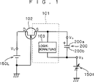
1 eine äquivalente Schaltung einer Halbleitervorrichtung nach einer ersten bevorzugten Ausführungsform dieser Erfindung; 1 an equivalent circuit of a semiconductor device according to a first preferred embodiment of this invention;
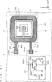
2 eine Draufsicht der Halbleitervorrichtungsstruktur nach der ersten bevorzugten Ausführungsform; 2 a plan view of the semiconductor device structure according to the first preferred embodiment;
3 bis 5 Querschnittsansichten der Halbleitervorrichtungsstruktur nach der ersten bevorzugten Ausführungsform; 3 to 5 Cross-sectional views of the semiconductor device structure according to the first preferred embodiment;
6 ein Schaltungsdiagramm der Halbleitervorrichtung nach der ersten bevorzugten Ausführungsform, wobei eine Spannungsquelle und ein Urladekapazitätselement direkt verbunden sind; 6 12 is a circuit diagram of the semiconductor device according to the first preferred embodiment, wherein a voltage source and a bootstrap capacitance element are directly connected;
7 ein Schaltungsdiagramm der Halbleitervorrichtung nach der ersten bevorzugten Ausführungsform, wobei die Spannungsquelle und das Urladekapazitätselement durch einen Begrenzungswiderstand verbunden sind; 7 12 is a circuit diagram of the semiconductor device according to the first preferred embodiment, wherein the voltage source and the bootstrap capacitance element are connected by a limiting resistor;
8A und 8B Illustrationen von Ladeeigenschaften beim Laden des Urladekapazitätselements; 8A and 8B Illustrations of loading characteristics when loading the boot capacity element;
9A bis 9C eine Darstellung, wie eine Verarmungsschicht ausgebildet wird; 9A to 9C a representation of how a depletion layer is formed;
10 bis 12 Querschnittsansichten einer Halbleitervorrichtungsstruktur nach einer zweiten bevorzugten Ausführungsform dieser Erfindung; 10 to 12 Cross-sectional views of a semiconductor device structure according to a second preferred embodiment of this invention;
13 eine Draufsicht einer Halbleitervorrichtungsstruktur nach einer dritten bevorzugten Ausführungsform dieser Erfindung; 13 a plan view of a semiconductor device structure according to a third preferred embodiment of this invention;
14 eine Querschnittsansicht der Halbleitervorrichtungsstruktur nach der dritten bevorzugten Ausführungsform; 14 a cross-sectional view of the semiconductor device structure according to the third preferred embodiment;
15 eine Querschnittsansicht einer Struktur einer Modifikation der Halbleitervorrichtung nach der dritten bevorzugten Ausführungsform; 15 FIG. 12 is a cross-sectional view of a structure of a modification of the semiconductor device according to the third preferred embodiment; FIG.
16 eine Draufsicht einer Halbleitervorrichtungsstruktur nach einer vierten bevorzugten Ausführungsform dieser Erfindung; 16 a plan view of a semiconductor device structure according to a fourth preferred embodiment of this invention;
17 eine Querschnittsansicht der Halbleitervorrichtungsstruktur nach der vierten bevorzugten Ausführungsform; 17 12 is a cross-sectional view of the semiconductor device structure according to the fourth preferred embodiment;
18 eine Draufsicht einer Halbleitervorrichtungsstruktur nach einer fünften bevorzugten Ausführungsform dieser Erfindung; 18 a plan view of a semiconductor device structure according to a fifth preferred embodiment of this invention;
19 bis 21 Querschnittsansichten der Halbleitervorrichtungsstruktur nach der fünften bevorzugten Ausführungsform; 19 to 21 Cross-sectional views of the semiconductor device structure according to the fifth preferred embodiment;
22 eine Darstellung der Beziehung zwischen einem Anlegepotential Vg und einem Anfangsladestrom; 22 a representation of the relationship between an application potential V g and an initial charging current;
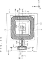
23 eine Draufsicht einer Halbleitervorrichtungsstruktur nach einer sechsten bevorzugten Ausführungsform dieser Erfindung; 23 a plan view of a semiconductor device structure according to a sixth preferred embodiment of this invention;
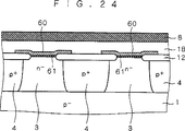
24 eine Querschnittsansicht der Halbleitervorrichtungsstruktur nach der sechsten bevorzugten Ausführungsform; 24 a cross-sectional view of the semiconductor device structure according to the sixth preferred embodiment;
25 eine Draufsicht einer Halbleitervorrichtungsstruktur nach einer siebten bevorzugten Ausführungsform dieser Erfindung; 25 a plan view of a semiconductor device structure according to a seventh preferred embodiment of this invention;
26 bis 28 Querschnittsansichten der Halbleitervorrichtungsstruktur nach der siebten bevorzugten Ausführungsform; 26 to 28 Cross-sectional views of the semiconductor device structure according to the seventh preferred embodiment;
29 eine äquivalente Schaltung der Halbleitervorrichtung nach der siebten bevorzugten Ausführungsform; 29 an equivalent circuit of the semiconductor device according to the seventh preferred embodiment;
30 eine Darstellung eins parasitären Bipolartransistors; 30 a representation of a parasitic bipolar transistor;
31 eine Draufsicht einer Halbleitervorrichtungsstruktur nach einer achten bevorzugten Ausführungsform dieser Erfindung; 31 a plan view of a semiconductor device structure according to a eighth preferred embodiment of this invention;
32A bis 32C Darstellungen von Potentialsignalverläufen eines Potentials Vb, eines Potentials V0 bzw. eines Detektionssignals DS0; 32A to 32C Representations of Potentialsignalverläufen a potential V b , a potential V0 and a detection signal DS0;
33 eine Draufsicht einer Halbleitervorrichtungsstruktur nach einer neunten bevorzugten Ausführungsform dieser Erfindung; 33 a plan view of a semiconductor device structure according to a ninth preferred embodiment of this invention;
34A bis 34C Darstellungen von Potentialsignalverläufen des Potentials Vb, des Potentials V0 bzw. eines Detektionssignals DS1. 34A to 34C Representations of Potentialsignalverläufen the potential V b , the potential V0 and a detection signal DS1.
Erste bevorzugte AusführungsformFirst preferred embodiment
1 zeigt eine äquivalente Schaltung einer Halbleitervorrichtung nach einer ersten bevorzugten Ausführungsform dieser Erfindung und von deren peripheren Schaltungen. Die Halbleitervorrichtung der ersten bevorzugten Ausführungsform ist ein HVIC, das eine Logikschaltung 103, die, wie später diskutiert wird, in einem Hochpotentialinselbereich 101 ausgebildet ist, und einen n-Kanal-Typ JFET (junction FET/Übergangs-FET) 102 beinhaltet, dessen Source mit der Logikschaltung 103 verbunden ist. Die Source des JFET 102 ist zum Beispiel mit einem positiven Leistungsversorgungsanschluß der Logikschaltung 103 verbunden. 1 Fig. 12 shows an equivalent circuit of a semiconductor device according to a first preferred embodiment of this invention and its peripheral circuits. The semiconductor device of the first preferred embodiment is an HVIC, which is a logic circuit 103 which, as discussed later, are in a high potential island region 101 is formed, and an n-channel type JFET (junction FET) 102 includes, its source with the logic circuit 103 connected is. The source of the JFET 102 is, for example, a positive power supply terminal of the logic circuit 103 connected.
Das eine Ende 200a und das andere Ende 200b eines Urladekapazitätselements 200 sind mit der Logikschaltung 103 verbunden. In diesem Beispiel sind das eine Ende 200a und das andere Ende 200b mit dem positiven Leistungsversorgungsanschluß bzw. einem negativen Leistungsversorgungsanschluß der Logikschaltung 103 verbunden. Das Potential an dem einen Ende 200a wird als ein ”Potential Vb” bezeichnet.The one end 200a and the other end 200b a boot capacity element 200 are with the logic circuit 103 connected. In this example, that's one end 200a and the other end 200b to the positive power supply terminal and a negative power supply terminal of the logic circuit, respectively 103 connected. The potential at one end 200a is referred to as a "potential V b ".
Der JFET 102 weist ein mit einer Spannungsquelle 150L verbundenes Drain und ein mit einem Massepotential versorgtes Gate auf. Ferner ist eine nicht gezeigte Last mit dem anderen Ende 200b des Urladekapazitätselements 200 verbunden und das Potential an dem Knoten variiert mit den Lastbedingungen. Zum Beispiel wird das Knotenpotential ein Massepotential oder ein hohes Potential von einigen hundert Volt (im weiteren als ein ”Potential VH” bezeichnet). Es wird deshalb angenommen, wie in 1 gezeigt ist, daß eine virtuelle Spannungsquelle 150H, die eine virtuelle variable Spannungsquelle ist, mit dem anderen Ende 200b verbunden ist, und ein Ausgangspotential VS an der virtuellen Spannungsquelle 150H wird ein Massepotential oder das Potential VH.The JFET 102 indicates with a voltage source 150L connected drain and a supplied to a ground potential gate. Further, a load, not shown, is at the other end 200b the boot capacity element 200 and the potential at the node varies with the load conditions. For example, the node potential becomes a ground potential or a high potential of several hundred volts (hereinafter referred to as a "potential V H "). It is therefore assumed as in 1 it is shown that a virtual voltage source 150H , which is a virtual variable voltage source, with the other end 200b is connected, and an output potential V S at the virtual voltage source 150H becomes a ground potential or the potential V H.
Die mit dem anderen Ende 200b des Urladekapazitätselements 200 verbundene Last kann zwei IGBT beinhalten, die Totem-Poleverbunden zwischen das Potential VH und ein Massepotential geschaltet sind, wobei der Knoten zwischen jenen beiden IGBT mit dem anderen Ende 200b verbunden ist. Die zwei IGBT führen zu voneinander verschiedenen Zeiten Schaltvorgänge durch und versorgen die mit dem Knoten zwischen ihnen verbundene Last mit dem Potential VH oder einem Massepotential. Die Spannungsquelle 150L ist z. B. eine Konstantspannungsquelle mit einem Ausgangspotential VL von einigen Dutzend Volt.The one with the other end 200b the boot capacity element 200 The connected load may include two IGBTs connected totem pole connections between the potential V H and a ground potential, the node between those two IGBTs having the other end 200b connected is. The two IGBTs perform switching operations at mutually different times and supply the load connected to the node between them with the potential V H or a ground potential. The voltage source 150L is z. B. a constant voltage source with an output potential V L of a few tens of volts.
Als nächstes wird der Betrieb der Halbleitervorrichtung nach der ersten bevorzugten Ausführungsform diskutiert. Wenn bei ungeladenem Urladekapazitätselement 200 das Ausgangspotential VS an der virtuellen Spannungsquelle 150H ein Massepotential (0V) ist, wird das Urladekapazitätselement 200 durch den JFET 102 mit der elektrischen Ladung von der Spannungsquelle 150L versorgt, so daß es geladen wird. Folglich wird die Spannung VL (= VL – 0V) in dem Urladekapazitätselement 200 akkumuliert. Währenddessen ist die Spannung VL an die Leistungsversorgung der Logikschaltung 103 angelegt, was den Betrieb der Logikschaltung 103 beeinflußt.Next, the operation of the semiconductor device according to the first preferred embodiment will be discussed. When with uncharged boot capacity element 200 the output potential V S at the virtual voltage source 150H is a ground potential (0V), becomes the boot capacity element 200 through the JFET 102 with the electrical charge from the voltage source 150L supplied so that it is loaded. As a result, the voltage becomes V L (= V L - 0V) in the bootstrap capacitance element 200 accumulated. Meanwhile, the voltage V L to the Power supply of the logic circuit 103 created, indicating the operation of the logic circuit 103 affected.
Wenn mit geladenem Urladekapazitätselement 200 das Ausgangspotential VS an der virtuellen Spannungsquelle 150H das Potential VH wird, steigt das Sourcepotential an dem JFET 102 um das Potential VH an, sodass es (VL + VH) wird, weil, wie später diskutiert wird, von der Source zu dem Drain des JFET 102 kaum ein Strom fließt. Folglich kommt die Stromversorgung von der Spannungsquelle 150L zu dem positiven Leistungsversorgungsanschluß der Logikschaltung 103 zu einem Halt und die elektrische Ladung in dem Urladekapazitätselement 200 wird an den positiven Leistungsversorgungsanschluß der Logikschaltung 103 geliefert. Das heißt, ein Potential (VL + VH) liegt an dem positiven Leistungsversorgungsanschluß der Logikschaltung 103 an und das Potential VH an dem negativen Leistungsversorgungspotential. Auf diese Weise wird immer die Spannung VL an die Leistungsversorgung der Logikschaltung 103 geliefert, was ermöglicht, daß die Logikschaltung 103 unabhängig von dem Wert des Ausgangspotentials VS an der virtuellen Spannungsquelle 150H mit einer konstanten Spannungsquelle arbeitet.When loaded with boot capacity element 200 the output potential V S at the virtual voltage source 150H the potential becomes V H , the source potential on the JFET rises 102 around the potential V H , so that it becomes (V L + V H ) because, as discussed later, from the source to the drain of the JFET 102 hardly any electricity flows. Consequently, the power supply comes from the power source 150L to the positive power supply terminal of the logic circuit 103 to a stop and the electric charge in the boot capacity element 200 is applied to the positive power supply terminal of the logic circuit 103 delivered. That is, a potential (V L + V H ) is applied to the positive power supply terminal of the logic circuit 103 and the potential V H at the negative power supply potential. In this way, the voltage V L is always applied to the power supply of the logic circuit 103 delivered, which allows the logic circuit 103 regardless of the value of the output potential V S at the virtual voltage source 150H works with a constant voltage source.
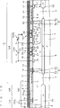
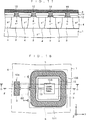
Als nächstes wird die Struktur der Halbleitervorrichtung nach der ersten bevorzugten Ausführungsform diskutiert. 2 ist eine schematische Draufsicht der Halbleitervorrichtungsstruktur und die 3 bis 5 sind Querschnittsansichten, die entlang den jeweiligen durch die Pfeile in 2 bezeichneten Linien A-A bis C-C genommen sind. Aus Gründen der Einfachheit ist eine Isolierschicht 8 in den 3 bis 5 nicht in 2 gezeigt, die nur die Elektroden 13 und 15 der auf einer Isolierschicht 18 ausgebildeten Elektroden zeigt. Dies trifft ebenfalls auf die folgenden Draufsichten zu.Next, the structure of the semiconductor device according to the first preferred embodiment will be discussed. 2 FIG. 12 is a schematic plan view of the semiconductor device structure and FIGS 3 to 5 are cross-sectional views taken along the respective one by the arrows in FIG 2 designated lines AA to CC are taken. For the sake of simplicity, an insulating layer 8th in the 3 to 5 not in 2 shown only the electrodes 13 and 15 on an insulating layer 18 trained electrodes shows. This also applies to the following plan views.
In der folgenden Erklärung bezeichnen die Symbole ”p”, ”p+”, ”p–”, ”n+”, ”n–” die Dotierungsleitungstypen und Dotierungskonzentrationen der Halbleitervorrichtung. Die Dotierungskonzentration steigt in der Reihenfolge ”p–”, ”p”, ”p+” an und ist bei ”n+” größer als bei ”n–”. Ferner ist die Dotierungskonzentration bei ”p”, ”p+” größer als bei ”n–” und ist bei ”p–”, ”p” niedriger als bei ”n+”.In the following explanation, the symbols "p", "p + ", "p - ", "n + ", "n - " denote the doping line types and doping concentrations of the semiconductor device. The doping concentration increases in the order "p - ", "p", "p + " and is greater at "n + " than at "n - ". Further, the doping concentration at "p", "p + " is greater than at "n - " and lower at "p - ", "p" than at "n + ".
Bei der Halbleitervorrichtung der ersten bevorzugten Ausführungsform ist, wie in den 2 bis 5 gezeigt, eine n–-Halbleiterschicht 3 auf einem p–-Halbleitersubstrat 1 ausgebildet. Sich von einer oberen Oberfläche der n–-Halbleiterschicht 3 zu der Grenzfläche zwischen der n–-Halbleiterschicht 3 und dem p–-Halbleitersubstrat 1 erstreckend ist ein p+-Dotierungsbereich 4 in der n–-Halbleiterschicht 3 ausgebildet. Der p+-Dotierungsbereich 4 ist derart ausgebildet, daß er einen Teil der n–-Halbleiterschicht 3 umgibt, und definiert den Hochpotentialinselbereich 101, in dem die Logikschaltung 103 angeordnet ist, einen Niedrigpotentialinselbereich 104, an den das Ausgangspotential VL an der Spannungsquelle 150L anliegt, und einen Schlitzbereich 105 in der n–-Halbleiterschicht 3.In the semiconductor device of the first preferred embodiment, as in FIGS 2 to 5 shown an n - semiconductor layer 3 on a p - semiconductor substrate 1 educated. Extending from an upper surface of the n - semiconductor layer 3 to the interface between the n - semiconductor layer 3 and the p - semiconductor substrate 1 extending is a p + doping region 4 in the n - semiconductor layer 3 educated. The p + doping region 4 is formed so as to form part of the n - semiconductor layer 3 surrounds and defines the high potential island area 101 in which the logic circuit 103 is arranged, a low potential island area 104 to which the output potential V L at the voltage source 150L is applied, and a slot area 105 in the n - semiconductor layer 3 ,
Die n–-Halbleiterschicht 3 in dem Hochpotentialinselbereich 101 und die n–-Halbleiterschicht 3 in dem Niedrigpotentialinselbereich 104 sind durch die n–-Halbleiterschicht 3 in dem Schlitzbereich 105 verbunden. Anders ausgedrückt ist die n–-Halbleiterschicht 3 in dem Schlitzbereich 105 zwischen den n–-Halb-leiterschichten 3 in dem Hochpotentialinselbereich 101 und dem Niedrigpotentialinselbereich 104 angeordnet und ist mit beiden verbunden.The n - semiconductor layer 3 in the high potential island area 101 and the n - semiconductor layer 3 in the low potential island area 104 are through the n - semiconductor layer 3 in the slot area 105 connected. In other words, the n - semiconductor layer 3 in the slot area 105 between the n - half semiconductor layers 3 in the high potential island area 101 and the low potential island area 104 arranged and is connected to both.
Wie in 2 gezeigt ist die n–-Halbleiterschicht 3 in dem Hochpotentialinselbereich 101 in Draufsicht wie ein Quadrat geformt und weist eine Mehrzahl von Seiten auf. Die n–-Halbleiterschichten 3 in dem Niedrigpotentialinselbereich 104 und dem Schlitzbereich 105 sind in Draufsicht wie ein Rechteck geformt.As in 2 the n - semiconductor layer is shown 3 in the high potential island area 101 formed in plan view like a square and has a plurality of sides. The n - semiconductor layers 3 in the low potential island area 104 and the slot area 105 are shaped like a rectangle in plan view.
In Draufsicht sind der Hochpotentialinselbereich 101, der Schlitzbereich 105 und der Niedrigpotentialinselbereich 104 linear in dieser Reihenfolge entlang der Richtung der X-Achse angeordnet. Und in Draufsicht ist eine Breite W der n–-Halbleiterschicht 3 in der Richtung der Y-Achse in dem Schlitzbereich 105 derart gesetzt, daß sie schmaler ist, als eine Breite HW der n–-Halbleiterschicht 3 in der Richtung der Y-Achse in dem Hochpotentialinselbereich 101. Hierbei ist die Richtung der Y-Achse senkrecht zu der Richtung der X-Achse. Deshalb können wir sagen, daß die Breite der n–-Halbleiterschicht 3 in dem Schlitzbereich 105 in der Richtung senkrecht zu der Richtung, entlang der der Hochpotentialinselbereich 101 und der Schlitzbereich 105 angeordnet sind, schmaler ist, als die in dem Hochpotentialinselbereich 101. Die Z-Achse in 2 ist orthogonal zu der X- und der Y-Achse. Das heißt, die X-, die Y- und die Z-Achse bilden ein orthogonales Koordinatensystem.In plan view are the high potential island area 101 , the slot area 105 and the low potential island area 104 arranged linearly in this order along the direction of the X-axis. And in plan view, a width W of the n - semiconductor layer 3 in the direction of the Y-axis in the slot area 105 is set to be narrower than a width HW of the n - semiconductor layer 3 in the Y-axis direction in the high potential island region 101 , Here, the direction of the Y-axis is perpendicular to the direction of the X-axis. Therefore we can say that the width of the n - semiconductor layer 3 in the slot area 105 in the direction perpendicular to the direction along which the high potential island region 101 and the slot area 105 are narrower than those in the high potential island region 101 , The z-axis in 2 is orthogonal to the X and Y axes. That is, the X, Y, and Z axes form an orthogonal coordinate system.
Wie oben diskutiert, ist die Breite W der n–-Halbleiterschicht 3 in dem Schlitzbereich 105 niedriger als die Breite HW der n–-Halbleiterschicht 3 in dem Hochpotentialinselbereich 101. Folglich kann in Draufsicht, wie in 2 gezeigt, die n–-Halbleiterschicht 3 in dem Schlitzbereich 105 teilweise mit einer Seite der n–-Halbleiterschicht 3 in dem Hochpotentialinselbereich 101 verbunden sein.As discussed above, the width W is the n -type semiconductor layer 3 in the slot area 105 lower than the width HW of the n - semiconductor layer 3 in the high potential island area 101 , Consequently, in plan view, as in FIG 2 shown the n - semiconductor layer 3 in the slot area 105 partially with one side of the n - semiconductor layer 3 in the high potential island area 101 be connected.
An der Grenzfläche zwischen der n–-Halbleiterschicht 3 und dem p–-Halbleitersubstrat 1 in dem Hochpotentialinselbereich 101 ist selektiv ein n+-vergrabener Dotierungsbereich 2 ausgebildet. Die Logikschaltung 103 ist in der n–-Halbleiterschicht 3 oberhalb des n+-vergrabenen Dotierungsbereichs 2 ausgebildet.At the interface between the n - semiconductor layer 3 and the p - semiconductor substrate 1 in the high potential island area 101 is selectively an n + buried dopant region 2 educated. The logic circuit 103 is in the n - semiconductor layer 3 above the n + buried doping region 2 educated.
Die Logikschaltung 103 beinhaltet zum Beispiel einen p-Kanal MOFET 130 und einen n-Kanal MOSFET 131. Der p-Kanal MOSFET 130 weist einen p+-Drainbereich 31, einen p+-Sourcebereich 32 und eine Gateelektrode 36 auf. Der Drainbereich 31 und der Sourcebereich 32 sind mit einem vorbestimmten Abstand in der oberen Oberfläche der n–-Halbleiterschicht 3 ausgebildet und die Gateelektrode 36 ist über eine Gateisolierschicht 34 auf der n–-Halbleiterschicht 3 zwischen dem Drainbereich 31 und dem Sourcebereich 32 ausgebildet. Ferner ist in der oberen Oberfläche der n–-Halbleiterschicht 3 ein n+-Dotierungsbereich 30 mit einem vorbestimmten Abstand benachbart zu dem Drainbereich 31 ausgebildet.The logic circuit 103 includes, for example, a p-channel MOFET 130 and an n-channel MOSFET 131 , The p-channel MOSFET 130 has a p + drain region 31 , a p + source area 32 and a gate electrode 36 on. The drainage area 31 and the source area 32 are at a predetermined distance in the upper surface of the n - semiconductor layer 3 formed and the gate electrode 36 is over a gate insulating layer 34 on the n - semiconductor layer 3 between the drainage area 31 and the source area 32 educated. Further, in the upper surface of the n - semiconductor layer 3 an n + doping region 30 at a predetermined distance adjacent to the drain region 31 educated.
Der n-Kanal MOSFET 131 ist benachbart zu dem p-Kanal MOSFET 130 angeordnet und in einem p-Grabenbereich 20 in der oberen Oberflache der n–Halbleiterschicht 3 ausgebildet. Der n-Kanal MOSFET 131 weist einen n+-Drainbereich 23, einen Sourcebereich 22 und eine Gateelektrode 26 auf. Der Drainbereich 23 und der Sourcebereich 22 sind mit vorbestimmtem Abstand in einer oberen Oberfläche des p-Grabenbereichs 20 ausgebildet und die Gateelektrode 26 ist über eine Gateisolierschicht 24 auf dem p-Grabenbereich 20 zwischen dem Drainbereich 23 und dem Sourcebereich 22 ausgebildet. Ferner ist in der oberen Oberfläche des p-Grabenbereichs 20 ein p+-Dotierungsbereich 21 mit vorbestimmtem Abstand benachbart zu dem Sourcebereich 22 ausgebildet.The n-channel MOSFET 131 is adjacent to the p-channel MOSFET 130 arranged and in a p-trench area 20 in the upper surface of the n - type semiconductor layer 3 educated. The n-channel MOSFET 131 has an n + drain region 23 , a source area 22 and a gate electrode 26 on. The drainage area 23 and the source area 22 are at a predetermined distance in an upper surface of the p-trench region 20 formed and the gate electrode 26 is over a gate insulating layer 24 on the p-trench area 20 between the drainage area 23 and the source area 22 educated. Further, in the upper surface of the p-trench region 20 a p + doping region 21 at a predetermined distance adjacent to the source region 22 educated.
Ebenfalls in der oberen Oberfläche der n–-Halbleiterschicht 3 in dem Hochpotentialinselbereich 101 ist ein n+-Dotierungsbereich 5, der n+-Dotierungsbereiche 5a und 5b beinhaltet, ausgebildet. Der n+-Dotierungsbereich 5 ist von der oberen Oberfläche der n–-Halbleiterschicht 3 bis zu dem n+-vergrabenen Dotierungsbereich 2 vorgesehen und mit der Peripherie des n+-vergrabenen Dotierungsbereichs 2 verbunden. Der n+-Dotierungsbereich 5 ist derart ausgebildet, daß er die Logikschaltung 103 umgibt. Der n+-Dotierungsbereich 5a ist in der Nähe der oberen Oberfläche der n–-Halbleiterschicht 3 ausgebildet und der n+-Dotierungsbereich 5b ist mit dem n+-Dotierungsbereich 5a verbunden und erstreckt sich zu dem n+-vergrabenen Dotierungsbereich 2.Also in the upper surface of the n - semiconductor layer 3 in the high potential island area 101 is an n + doping area 5 , the n + doping areas 5a and 5b includes, trained. The n + doping area 5 is from the upper surface of the n - semiconductor layer 3 to the n + buried doping region 2 and with the periphery of the n + buried doping region 2 connected. The n + doping area 5 is designed to be the logic circuit 103 surrounds. The n + doping area 5a is near the top surface of the n - semiconductor layer 3 trained and the n + -Dotierungsbereich 5b is with the n + doping range 5a and extends to the n + buried doping region 2 ,
Ferner ist in der oberen Oberfläche der n–-Halbleiterschicht 3 in dem Hochpotentialinselbereich 101 ein p+-Dotierungsbereich 7 entlang dem Umfang des Hochpotentialinselbereichs 101 außerhalb des n+-Dotierungsbereichs 5 ausgebildet, der mit dem p+-Dotierungsbereich 4 verbunden ist. Der p+-Dotierungsbereich 7 ist in der n–-Halbleiterschicht 3 an der Grenze zwischen dem Hochpotentialinselbereich 101 und dem Schlitzbereich 105 nicht vorgesehen. In der oberen Oberfläche der n–-Halbleiterschicht 3 in dem Niedrigpotentialinselbereich 104 ist ein n+-Dotierungsbereich 6 getrennt von dem p+-Dotierungsbereich 4 ausgebildet.Further, in the upper surface of the n - semiconductor layer 3 in the high potential island area 101 a p + doping region 7 along the circumference of the high potential island region 101 outside the n + doping range 5 formed with the p + doping region 4 connected is. The p + doping region 7 is in the n - semiconductor layer 3 at the boundary between the high potential island area 101 and the slot area 105 not provided. In the upper surface of the n - semiconductor layer 3 in the low potential island area 104 is an n + doping area 6 separated from the p + doping region 4 educated.
Eine Oxidschicht 12 ist auf den oberen Oberflächen der n–-Halbleiterschichten 3 in dem Hochpotentialinselbereich 101, dem Niedrigpotentialinselbereich 104 und dem Schlitzbereich 105, auf einer oberen Oberfläche des p+-Dotierungsbereichs 4 und auf der oberen Oberfläche des p-Grabenbereichs 20 derart ausgebildet, daß die n+-Dotierungsbereiche 5 und 30, die p+-Dotierungsbereiche 7 und 21, die Sourcebereiche 22 und 32, die Drainbereiche 23 und 31 und der n+-Dotierungsbereich 6 freigelegt sind. Auf der Oxidschicht 12 ist, auf der oberen Oberfläche der n–-Halbleiterschichten 3 zwischen dem n+-Dotierungsbereich 5 und dem p+-Dotierungsbereich 7 bereitgestellt, eine Mehrzahl von Elektroden 9 derart ausgebildet, daß sie den n+-Dotierungsbereich 5 und die Logikschaltung 103 in Draufsicht umgeben. Die Mehrzahl von Elektroden 9 bildet mehrere Feldplatten für eine verbesserte Durchbruchspannung der Halbleitervorrichtung der ersten bevorzugten Ausführungsform. Die Elektrode 9 sowie die Gateelektroden 26 und 36 bestehen z. B. aus Polysilizium.An oxide layer 12 is on the upper surfaces of the n - semiconductor layers 3 in the high potential island area 101 , the low-potential island area 104 and the slot area 105 , on an upper surface of the p + doping region 4 and on the upper surface of the p-trench region 20 formed such that the n + doping regions 5 and 30 , the p + doping regions 7 and 21 , the source areas 22 and 32 , the drain areas 23 and 31 and the n + doping region 6 are exposed. On the oxide layer 12 is, on the upper surface of the n - semiconductor layers 3 between the n + doping region 5 and the p + doping region 7 provided, a plurality of electrodes 9 designed to be the n + doping region 5 and the logic circuit 103 surrounded in plan view. The majority of electrodes 9 forms a plurality of field plates for an improved breakdown voltage of the semiconductor device of the first preferred embodiment. The electrode 9 as well as the gate electrodes 26 and 36 exist z. B. of polysilicon.
Bei der Halbleitervorrichtung der ersten bevorzugten Ausführungsform ist die Isolierschicht 18 derart ausgebildet, daß sie die n–-Halbleiterschichten 3, die Oxidschicht 12, die Gateelektroden 26 und 36 und die Elektroden 9 bedeckt. Durch die Isolierschicht 18 hindurch sind eine Elektrode 16 mit dem n+-Dotierungsbereich 6, die Elektrode 15 mit dem n+-Dotierungsbereich 5 und eine Elektrode 17 mit dem p+-Dotierungsbereich 7 verbunden. Eine Elektrode 35 ist durch die Isolierschicht 18 hindurch mit dem Drainbereich 31, dem Sourcebereich 32 und der Gateelektrode 36 des p-Kanal MOSFET 130 und dem n+-Dotierungsbereich 30 verbunden. Eine Elektrode 25 ist durch die Isolierschicht 18 hindurch mit dem Drainbereich 23, dem Sourcebereich 22 und der Gateelektrode 26 des n-Kanal MOSFET 131 und dem p+-Dotierungsbereich 21 verbunden.In the semiconductor device of the first preferred embodiment, the insulating layer is 18 formed such that they are the n - semiconductor layers 3 , the oxide layer 12 , the gate electrodes 26 and 36 and the electrodes 9 covered. Through the insulating layer 18 through are an electrode 16 with the n + doping region 6 , the electrode 15 with the n + doping region 5 and an electrode 17 with the p + doping region 7 connected. An electrode 35 is through the insulating layer 18 through to the drain area 31 , the source area 32 and the gate electrode 36 of the p-channel MOSFET 130 and the n + doping region 30 connected. An electrode 25 is through the insulating layer 18 through to the drain area 23 , the source area 22 and the gate electrode 26 of the n-channel MOSFET 131 and the p + doping region 21 connected.
Die Elektrode 15 ist entlang dem n+-Dotierungsbereich 5, mit dem die Elektrode 15 selbst verbunden ist, angeordnet, so daß sie die Logikschaltung 103 in Draufsicht umgibt. Die Elektrode 15 ist durch eine Elektrode 13 mit der Elektrode 35 auf dem Drainbereich 31 und dem n+-Dotierungsbereich 30 verbunden. Die Elektrode 17 ist entlang dem p+-Dotierungsbereich 7, mit dem die Elektrode 17 selbst verbunden ist, ausgebildet, so daß sie die Logikschaltung 103 und die Elektrode 15 in Draufsicht umgibt.The electrode 15 is along the n + doping region 5 with which the electrode 15 itself is connected, arranged so that it is the logic circuit 103 surrounds in plan view. The electrode 15 is through an electrode 13 with the electrode 35 on the drain area 31 and the n + doping region 30 connected. The electrode 17 is along the p + doping region 7 with which the electrode 17 itself is connected, trained so that it is the logic circuit 103 and the electrode 15 surrounds in plan view.
Eine Mehrzahl von schwebenden Elektroden 10 ist auf der Isolierschicht 18 über den Elektroden 9 angeordnet und kapazitive Kopplung zwischen den Elektroden 10 und 9 verbessert die Durchbruchsspannung der Halbleitervorrichtung der ersten bevorzugten Ausführungsform. Die Isolierschicht 8 ist auf der Isolierschicht 18 derart ausgebildet, daß sie die jeweiligen Elektroden bedeckt.A plurality of floating electrodes 10 is on the insulating layer 18 over the electrodes 9 arranged and capacitive coupling between the electrodes 10 and 9 improves the Breakdown voltage of the semiconductor device of the first preferred embodiment. The insulating layer 8th is on the insulating layer 18 formed so as to cover the respective electrodes.
Bei der Halbleitervorrichtung der ersten bevorzugten Ausführungsform ist der parasitäre JFET 102 derart ausgebildet, daß beide Endabschnitte in der Richtung der X-Achse der n–-Halbleiterschicht 3 in dem Schlitzbereich 105 als dessen Source und Drain dienen und der die n–-Halbleiterschicht 3 in der Richtung der Y-Achse dazwischenliegend einschließende p+-Dotierungsbereich 4 dient als dessen Gate. Der Betrieb dieses JFET 102 ermöglicht es, daß ausreichend elektrische Ladung zu dem Urladekapazitätselement 200 geliefert wird, wie später diskutiert wird. Zwischen den beiden Endabschnitten arbeitet der eine auf der Seite des Niedrigpotentialinselbereichs 104 als das Drain des JFET 102 und der andere auf der Seite des Hochpotentialinselbereichs 101 als die Source.In the semiconductor device of the first preferred embodiment, the parasitic JFET is 102 formed such that both end portions in the direction of the X-axis of the n - semiconductor layer 3 in the slot area 105 serve as its source and drain and the n - semiconductor layer 3 in the direction of the Y-axis intervening p + -type doping region 4 serves as its gate. The operation of this JFET 102 allows sufficient electrical charge to the bootstrap capacity element 200 is delivered, as discussed later. Between the two end sections, one works on the side of the low potential island area 104 as the drain of the JFET 102 and the other on the high potential island region side 101 as the source.
Bei der Halbleitervorrichtung der ersten bevorzugten Ausführungsform mit der obigen Struktur wird ein Massepotential an die p+-Dotierungsbereiche 4 und 7 und das p–-Halbleitersubstrat 1 angelegt. Währenddessen wird das Ausgangspotential VL an der Spannungsquelle 150L an die Elektrode 16 angelegt, wodurch das Potential VL an die n–-Halbleiterschicht 3 in dem Niedrigpotentialinselbereich 104 und an das Drain des JFET 102 angelegt wird.In the semiconductor device of the first preferred embodiment having the above structure, a ground potential becomes the p + -type regions 4 and 7 and the p - semiconductor substrate 1 created. Meanwhile, the output potential V L becomes at the power source 150L to the electrode 16 applied, whereby the potential V L to the n - semiconductor layer 3 in the low potential island area 104 and to the drain of the JFET 102 is created.
Die mit dem p+-Dotierungsbereich 21 verbundene Elektrode 25 ist der negative Leistungsversorgungsanschluß der Logikschaltung 103, an den das Ausgangspotential VS an der virtuellen Spannungsquelle 150H angelegt ist. Die mit dem n+-Dotierungsbereich 30 verbundene Elektrode 35 ist der positive Leistungsversorgungsanschluß der Logikschaltung 103, der elektrisch mit dem einen Ende 200a des Urladekapazitätselements 200 verbunden ist. Entsprechend liegt das Potential Vb an dem Potential an der n–-Halbleiterschicht 3 in dem Hochpotentialinselbereich 101 und an der Source des JFET 102 an.The one with the p + doping region 21 connected electrode 25 is the negative power supply terminal of the logic circuit 103 to which the output potential V S at the virtual voltage source 150H is created. The one with the n + doping range 30 connected electrode 35 is the positive power supply terminal of the logic circuit 103 that is electrical to one end 200a the boot capacity element 200 connected is. Accordingly, the potential V b is at the potential at the n - semiconductor layer 3 in the high potential island area 101 and at the source of the JFET 102 at.
Wenn bei ungeladenem Urladekapazitätselement 200 das Potential VS ein Massepotential ist, wird wie oben diskutiert das Urladekapazitätselement 200 durch die Spannungsquelle 150L geladen. Der Ladestrom geht durch die n–-Halbleiterschicht 3 in dem Niedrigpotentialinselbereich 104, die n–-Halbleiterschicht 3 in dem Schlitzbereich 105, die ein Kanal des JFET 102 ist, und die n–-Halbleiterschicht 3 in dem Hochpotentialinselbereich 101 in dieser Reihenfolge, so daß er an das Urladekapazitätselement 200 geliefert wird.When with uncharged boot capacity element 200 the potential V S is a ground potential, as discussed above, the bootstrap capacitance element becomes 200 through the voltage source 150L loaded. The charging current passes through the n - semiconductor layer 3 in the low potential island area 104 , the n - semiconductor layer 3 in the slot area 105 which is a channel of the JFET 102 is, and the n - semiconductor layer 3 in the high potential island area 101 in that order, so that it connects to the boot capacity element 200 is delivered.
Auf diese Art wird bei der ersten bevorzugten Ausführungsform der Ladestrom an das Urladekapazitätselement 200 geliefert ohne durch einen pn-Übergang zu gehen. Deshalb kann das Potential Vb auf das Ausgangspotential VL an der Spannungsquelle 150 L erhöht werden.In this way, in the first preferred embodiment, the charging current is applied to the boot capacity element 200 delivered without going through a PN junction. Therefore, the potential V b at the output potential V L at the voltage source 150 L be increased.
Wenn das Ausgangspotential VS an der virtuellen Spannungsquelle 150H das Potential VH wird, wird nachdem das Urladekapazitätselement 200 geladen wurde das Potential Vb zu (VL + VH). Das resultierende Anlegen einer Umkehrspannung einer Höhe von einigen hundert Volt an einen pn-Übergang, der von der n–-Halbleiterschicht 3 in dem Schlitzbereich 105 und dem ihn in der Richtung der Y-Achse dazwischenliegend einschließenden p+-Dotierungsbereich 4 gebildet ist, führt zu dem Ausbilden einer Verarmungsschicht über fast die gesamte n–-Halbleiterschicht 3 in dem Schlitzbereich 105. Selbst wenn das Potential Vb zu (VL + VH) wird, was wie oben diskutiert höher als das Ausgangspotential VL an der Spannungsquelle 150L ist, fließt als ein Ergebnis die akkumulierte elektrische Ladung in dem Urladekapazitätselement 200 kaum in Richtung der n–-Halbleiterschicht 3 in dem Niedrigpotentialinselbereich 104, was dem Potential Vb ermöglicht (VL + VH) zu halten. Deshalb wird zu allen Zeiten die Spannung VL an die Leistungsversorgung der Logikschaltung 103 geliefert.When the output potential V S at the virtual power source 150H the potential V becomes H becomes after the bootstrap capacity element 200 the potential V b was charged to (V L + V H ). The resulting application of a reverse voltage of a few hundred volts to a pn junction, that of the n - semiconductor layer 3 in the slot area 105 and the p + doping region sandwiching it in the direction of the Y axis 4 is formed, forming a depletion layer over almost the entire n - semiconductor layer 3 in the slot area 105 , Even if the potential V b becomes (V L + V H ), which, as discussed above, is higher than the output potential V L at the voltage source 150L As a result, the accumulated electric charge flows in the bootstrap capacitance element 200 hardly in the direction of the n - semiconductor layer 3 in the low potential island area 104 , which allows the potential V b (V L + V H ) to hold. Therefore, at all times, the voltage V L is applied to the power supply of the logic circuit 103 delivered.
Wenn das Ausgangspotential VS an der virtuellen Spannungsquelle 150H das Potential VH wird, wird ferner eine Umkehrspannung in der Höhe von einigen hundert Volt an einen pn-Übergang angelegt, der von der n–-Halbleiterschicht 3 in dem Hochpotentialinselbereich 101 und dem ihn umgebenden p+-Dotierungsbereich 4 gebildet ist. Ein resultierender RESURF-Effekt führt zu dem Ausbilden einer Verarmungsschicht in der n–-Halbleiterschicht 3 in dem Hochpotentialinselbereich 101 gegenüber der Logikschaltung 103 bezüglich des n+-Dotierungsbereichs 5, d. h. in der gesamten n–-Halbleiterschicht 3 außerhalb des n+-Dotierungsbereichs 5 in dem Hochpotentialinselbereich 101. Die Logikschaltung 103 ist folglich von der Verarmungsschicht umgeben, wodurch eine Halbleitervorrichtung mit einer hohen Durchbruchspannung erzielt wird. Ein durch die schräge Linie in 2 bezeichneter RESURF-Isolationsbereich 106 zeigt einen groben Umriß eines Bereichs, in dem die Verarmungsschicht ausgebildet wird, wenn das Ausgangspotential VS an der virtuellen Spannungsquelle 150H das Potential VH wird.When the output potential V S at the virtual power source 150H When the potential becomes V H , a reverse voltage as high as a few hundred volts is also applied to a pn-junction, that of the n -type semiconductor layer 3 in the high potential island area 101 and the p + doping region surrounding it 4 is formed. A resulting RESURF effect results in the formation of a depletion layer in the n -type semiconductor layer 3 in the high potential island area 101 opposite the logic circuit 103 with respect to the n + doping region 5 ie in the entire n - semiconductor layer 3 outside the n + doping range 5 in the high potential island area 101 , The logic circuit 103 is thus surrounded by the depletion layer, whereby a semiconductor device with a high breakdown voltage is achieved. A through the oblique line in 2 designated RESURF isolation range 106 FIG. 12 shows a rough outline of a region in which the depletion layer is formed when the output potential V S at the virtual power source 150H the potential V H becomes.
Bei der Halbleitervorrichtung der ersten bevorzugten Ausführungsform ist eine Schaltung (nicht gezeigt), die die Spannungsquelle 150L als deren positive Leistungsversorgung verwendet, ebenfalls in der n–-Halbleiterschicht 3 ausgebildet, die in einem anderen als dem Niedrigpotentialinselbereich 104, dem Schlitzbereich 105 und dem Hochpotentialinselbereich 101 ist und die mit diesen Bereichen durch den p+-Dotierungsbereich 4 verbunden ist. Diese Schaltung wird im weiteren als eine ”Niedrigdurchbruchsspannungschaltung” bezeichnet.In the semiconductor device of the first preferred embodiment, a circuit (not shown) that is the voltage source 150L used as their positive power supply, also in the n - semiconductor layer 3 formed in a different than the low potential island area 104 , the slot area 105 and the high potential island area 101 is and those with these areas through the p + -doping area 4 connected is. This circuit will be referred to hereinafter as a "low breakdown voltage circuit".
Bei der Halbleitervorrichtung der ersten bevorzugten Ausführungsform, bei der der parasitäre JFET 102 derart ausgebildet ist, daß beide Endabschnitte der n–-Halbleiterschicht 3 in der Richtung der X-Achse in dem Schlitzbereich 105 als dessen Source und Drain dienen, und der die n–-Halbleiterschicht 3 in der Richtung der Y-Achse dazwischen liegend anschließende p+-Dotierungsbereich 4 als dessen Gate dient, kann auf diese Art das Urladekapazitätselement 200 durch den JFET 102 geladen werden. Dementsprechend wird der Ladestrom ohne durch einen pn-Übergang zu gehen an das Urladekapazitätselement 200 geliefert, was es ermöglicht, daß ausreichendere elektrische Ladung an das Urladekapazitätselement 200 geliefert wird als durch eine Diode. Als ein Ergebnis kann eine Halbleitervorrichtung mit exzellenten elektrischen Eigenschaften erhalten werden.In the semiconductor device of the first preferred embodiment, in which the parasitic JFET 102 is formed such that both end portions of the n - semiconductor layer 3 in the X-axis direction in the slot area 105 serve as its source and drain, and the n - semiconductor layer 3 lying in the direction of the Y-axis intervening p + -doping region 4 serves as its gate, in this way the boot capacity element 200 through the JFET 102 getting charged. Accordingly, the charging current without going through a pn junction to the boot capacity element 200 which allows for more sufficient electrical charge to the bootstrap capacity element 200 is delivered as by a diode. As a result, a semiconductor device having excellent electrical characteristics can be obtained.
Ferner ist bei der ersten bevorzugten Ausführungsform die Breite W der n–-Halbleiterschicht 3 in dem Schlitzbereich 105 derart gesetzt, daß sie kleiner ist, als die Breite HW der n–-Halbleiterschicht 3 in dem Hochpotentialinselbereich 101. Falls umgekehrt die Breite W derart gesetzt ist, daß sie nicht kleiner als die Breite HW ist, führt das Vergrößern der Breite HW zum Ausbilden einer Logikschaltung 103 großen Ausmaßes mit einer großen Grundfläche ebenfalls zu dem Verbreitern der Breite W, was es, selbst wenn das Potential VS auf ein hohes Potential gesetzt ist, für eine Verarmungsschicht erschwert, über fast die gesamte n–Halbleiterschicht 3 in dem Schlitzbereich 105 ausgebildet zu werden. Dies erhöht die Möglichkeiten von Leckverlust der akkumulierten elektrischen Ladung in dem Urladekapazitätselement 200 in Richtung der n–-Halbleiterschicht 3 in dem Schlitzbereich 105.Further, in the first preferred embodiment, the width W is the n -type semiconductor layer 3 in the slot area 105 set such that it is smaller than the width HW of the n - semiconductor layer 3 in the high potential island area 101 , Conversely, if the width W is set to be not smaller than the width HW, increasing the width HW results in forming a logic circuit 103 also large extent with a large footprint also widening the width W, which makes it difficult for a depletion layer, even if the potential V S is set to a high potential, over almost the entire n - type semiconductor layer 3 in the slot area 105 to be trained. This increases the chances of leakage of the accumulated electric charge in the bootstrap capacitance element 200 in the direction of the n - semiconductor layer 3 in the slot area 105 ,
Bei der ersten bevorzugten Ausführungsform, bei der die Breite W derart gesetzt ist, daß sie kleiner als die Breite HW ist, kann andererseits die Breite W bei dem Vergrößern der Breite HW zum Ausbilden einer Logikschaltung 103 großen Ausmaßes auf einem kleinen Wert gehalten werden, was es für eine Verarmungsschicht leicht macht, über fast die gesamte n–-Halbleiterschicht 3 in dem Schlitzbereich 105 ausgebildet zu werden. Deshalb kann der Leckverlust der akkumulierten elektrischen Ladung in dem Urladekapazitätselement 200 reduziert werden und das Potential Vb kann bei (VL + VH) gehalten werden.On the other hand, in the first preferred embodiment in which the width W is set to be smaller than the width HW, the width W may be increased to increase the width HW to form a logic circuit 103 to a small extent, making it light for a depletion layer, over almost the entire n - semiconductor layer 3 in the slot area 105 to be trained. Therefore, the leakage of the accumulated electric charge in the boot capacity element can 200 can be reduced and the potential V b can be maintained at (V L + V H ).
Außerdem ist es wünschenswert, daß die Breite W der n–-Halbleiterschicht 3 in dem Schlitzbereich 105 in dem folgenden Ausdruck (1) genügt: In addition, it is desirable that the width W of the n - semiconductor layer 3 in the slot area 105 in the following expression (1) suffice:
In dem obigen Ausdruck gilt Na >> Nd, es bezeichnet die dielektrische Konstante (F/cm) des in der Halbleitervorrichtung der ersten bevorzugten Ausführungsform verwendeten Halbleiters, q bezeichnet die Einheitsladungsmenge (C), Nd bezeichnet die Dotierungskonzentration (cm–3) der n–-Halbleiterschicht 3 und Na bezeichnet die Dotierungskonzentration (cm–3) des p+-Dotierungsbereichs 4.In the above expression, N a >> N d , which denotes the dielectric constant (F / cm) of the semiconductor used in the semiconductor device of the first preferred embodiment, q denotes the unit charge amount (C), N d denotes the doping concentration (cm -3 ) of the n - semiconductor layer 3 and N a denotes the doping concentration (cm -3 ) of the p + -type impurity region 4 ,
Der obige Ausdruck (1) ist ein Konditionalausdruck, bei dem der Endabschnitt auf der Drainseite der n–-Halbleiterschicht 3 in dem Schlitzbereich 105 beim Laden des Urladekapazitätselements 200 in einen Abschnürzustand eintritt. Als ein Ergebnis arbeitet der JFET 102 als ein Strombegrenzungswiderstand gegen den Ladestrom, wodurch die für die Spannungsquelle 150L erforderlich Strombelastbarkeit reduziert werden kann. Der Grund dafür wird unten beschrieben.The above expression (1) is a conditional expression in which the end portion on the drain side of the n - semiconductor layer 3 in the slot area 105 loading the boot capacity element 200 enters a pinch-off state. As a result, the JFET operates 102 as a current limiting resistor against the charging current, thereby reducing the voltage source 150L required current carrying capacity can be reduced. The reason for this is described below.
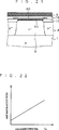
6 zeigt ein Schaltungsdiagramm der Halbleitervorrichtung der ersten bevorzugten Ausführungsform, bei der die Spannungsquelle 150L und das Urladekapazitätselement 200 direkt ohne Vorsehen des JFET 102 verbunden sind, und 7 zeigt ein Schaltungsdiagramm, bei dem ein Strombegrenzungswiderstand 201 anstelle des JFET 102 bereitgestellt ist. Die 8A und 8B illustrieren die Ladeeigenschaften der in den 6 und 7 gezeigten Schaltungen, wobei 8A das Verhältnis zwischen einem Ladestrom I und einer Ladezeit t bezüglich des Urladekapazitätselements 200 illustriert und 8B das Verhältnis zwischen dem Potential Vb und der Ladezeit t illustriert. Der Einfachheit halber ist die Logikschaltung 103 in den 6 und 7 nicht gezeigt. Die gestrichelten Linien und durchgehenden Linien in den 8A und 8B bezeichnen die Eigenschaften der in den 6 bzw. 7 gezeigten Schaltungen. 6 FIG. 12 is a circuit diagram of the semiconductor device of the first preferred embodiment in which the power source. FIG 150L and the boot capacity element 200 directly without providing the JFET 102 are connected, and 7 shows a circuit diagram in which a current limiting resistor 201 instead of the JFET 102 is provided. The 8A and 8B illustrate the charging characteristics of the in the 6 and 7 shown circuits, wherein 8A the relationship between a charging current I and a charging time t with respect to the boot capacity element 200 illustrated and 8B illustrates the relationship between the potential V b and the charging time t. For the sake of simplicity, the logic circuit 103 in the 6 and 7 Not shown. The dashed lines and solid lines in the 8A and 8B denote the properties of the in the 6 respectively. 7 shown circuits.
Wenn die Spannungsquelle 150L und das Urladekapazitätselement 200 wie in 6 gezeigt direkt verbunden sind, ist der Ladestrom direkt nach dem Start des Ladens (im weiteren als ein ”Anfangsladestrom” bezeichnet) beachtlich groß, wie in 8A gezeigt. Deswegen muß die Spannungsquelle 150L mit einer großen Strombelastbarkeit in diesem Fall verwendet werden, um eine mögliche Reduktion in dem Ausgangspotential VL an der Spannungsquelle 150L zu verhindern, wenn der Anfangsladestrom fließt. Da das Ausgangspotential VL wie oben ausgeführt als die positive Leistungsversorgung der nicht gezeigten Niedrigdurchbruchsspannungsschaltung verwendet ist, kann dessen Reduktion fehlerhaftes Arbeiten der Niedrigdurchbruchsspannungsschaltung verursachen. Deshalb muß die Spannungsquelle 150L mit einer großen Belastbarkeit vorbereitet sein, um die Reduktion zu verhindern. When the voltage source 150L and the boot capacity element 200 as in 6 are directly connected, charging current immediately after the start of charging (hereinafter referred to as a "start charging current") is remarkably large, as in 8A shown. Therefore, the voltage source must 150L with a high current carrying capacity in this case can be used to detect a possible reduction in the output potential V L at the voltage source 150L to prevent when the initial charging current flows. As described above, since the output potential V L is used as the positive power supply of the low breakdown voltage circuit, not shown, its reduction can cause erroneous operation of the low breakdown voltage circuit. Therefore, the voltage source must 150L be prepared with a high load capacity to prevent the reduction.
Wenn die Spannungsquelle 150L und das Urladekapazitätselement 200 wie in 7 gezeigt durch den Strombegrenzungswiderstand 201 verbunden sind, kann andererseits der Anfangsladestrom wie in 8A gezeigt reduziert werden. Folglich kann in diesem Fall die Spannungsquelle 150L mit einer kleineren Strombelastbarkeit verwendet werden, als wenn sie direkt verbunden sind. Das bedeutet, daß das Arbeiten des JFET 102 als ein Strombegrenzungswiderstand die Strombelastung der Spannungsquelle 150L reduzieren kann.When the voltage source 150L and the boot capacity element 200 as in 7 shown by the current limiting resistor 201 On the other hand, the initial charging current as in 8A be shown reduced. Consequently, in this case, the voltage source 150L be used with a smaller current carrying capacity than when they are directly connected. That means working the JFET 102 as a current limiting resistor, the current load of the voltage source 150L can reduce.
9 zeigt, wie die Verarmungsschicht in der n–-Halbleiterschicht 3 in dem Schlitzbereich 105 beim Laden des Urladekapazitätselements 200 ausgebildet wird, wobei es sich um eine Draufsicht von oben auf die n–-Halbleiterschicht 3 handelt. 9A zeigt eine Stufe, bei der Vb = 0 V gilt, d. h. wenn das Laden zu dem Urladekapazitätselement 200 beginnt, 9B zeigt eine Stufe, bei der 0 < Vb < VL gilt, d. h. die Periode, während der das Laden beginnt und abschließt und 9C zeigt eine Stufe, bei der Vb = VL gilt, d. h. wenn das Laden abgeschlossen ist. 9 shows how the depletion layer in the n - semiconductor layer 3 in the slot area 105 loading the boot capacity element 200 is formed, which is a top view of the n - semiconductor layer 3 is. 9A shows a stage where V b = 0 V, that is, when loading to the boot capacity element 200 begins 9B shows a stage where 0 <V b <V L , ie the period during which charging starts and ends and 9C shows a stage where V b = V L , that is, when the loading is completed.
Bei dem Beginn des Ladens erstrecken sich, wie in 9A gezeigt, Verarmungsschichten 250 von dem die n–-Halbleiterschicht 3 dazwischenliegend einschließendem p+-Dotierungsbereich 4 in die Richtung der Y-Achse an dem Endabschnitt der Drainseite der n–-Halbleiterschicht 3 in dem Schlitzbereich 105 und geraten in Kontakt zueinander, so daß in den Abschnürzustand eingetreten wird. Dies ermöglicht es dem JFET 102, am Anfang des Ladens als ein Strombegrenzungswiderstand zu arbeiten. Nachdem die elektrische Ladung in dem Urladekapazitätselement 200 akkumuliert ist und das Potential Vb ansteigt, wie in 9B gezeigt, erstrecken sich dann die Verarmungsschichten 250 auch von dem p+-Dotierungsbereich 4 an dem Endabschnitt auf der Sourceseite der n–-Halbleiterschicht 3 in dem Schlitzbereich 105.At the beginning of loading extend as in 9A shown, depletion layers 250 from which the n - semiconductor layer 3 intervening p + doping region 4 in the direction of the Y-axis at the end portion of the drain side of the n - semiconductor layer 3 in the slot area 105 and come in contact with each other, so that is entered into the Abschnürzustand. This allows the JFET 102 to work as a current limiting resistor at the beginning of charging. After the electric charge in the boot capacity element 200 is accumulated and the potential V b increases, as in 9B shown, then extend the depletion layers 250 also from the p + -doping area 4 at the end portion on the source side of the n - semiconductor layer 3 in the slot area 105 ,
Auf diese Art werden mit dem Fortschreiten des Ladens zu dem Urladekapazitätselement 200 die Verarmungsschichten 250 auch an dem Endabschnitt auf der Sourceseite der n–-Halbleiterschicht 3 in dem Schlitzbereich 105 ausgebildet, was ein Ansteigen der Impedanz des Kanals des JFET 102 einschließt. Das Ansteigen der Impedanz beeinflußt die Ladezeit jedoch nicht besonders, weil der erforderliche Ladestrom I mit voranschreitender Ladezeit t abfällt, wie in 8A gezeigt ist.In this way, as the loading progresses, it becomes the bootstrap capacity element 200 the depletion layers 250 also at the end portion on the source side of the n - semiconductor layer 3 in the slot area 105 formed, which is an increase in the impedance of the channel of the JFET 102 includes. However, the increase of the impedance does not particularly affect the charging time because the charging current I required decreases as the charging time t increases, as in FIG 8A is shown.
Wenn Vb auf VL ansteigt, wie in 9C gezeigt, sind dann die Verarmungsschichten 250 über die gesamte n–-Halbleiterschicht 3 in dem Schlitzbereich 105 ausgebildet. Selbst wenn das Potential VS danach auf das Potential VH gesetzt wird und das Potential Vb größer als das Potential VL wird, fließt deshalb die akkumulierte elektrische Ladung in dem Urladekapazitätselement 200 kaum in Richtung der n–-Halbleiterschicht 3 in dem Niedrigpotentialinselbereich 104, wodurch das Potential Vb zuverlässig auf (VL + VH) gehalten wird.When V b rises to V L , as in 9C are shown then the depletion layers 250 over the entire n - semiconductor layer 3 in the slot area 105 educated. Therefore, even if the potential V S is set to the potential V H and the potential V b becomes higher than the potential V L , the accumulated electric charge flows in the bootstrap capacitance element 200 hardly in the direction of the n - semiconductor layer 3 in the low potential island area 104 , whereby the potential V b is reliably maintained at (V L + V H ).
Auf diese Arten arbeitet der JFET 102 durch Setzen der Breite W der n–-Halbleiterschicht 3 in dem Schlitzbereich 105 so als ein Strombegrenzungswiderstand, daß der Ausdruck (1) erfüllt ist, wodurch die erforderliche Strombelastbarkeit für die Spannungsquelle 150L, die ein Potential an die n–-Halbleiterschicht 3 in dem Niedrigpotentialinselbereich 104 liefert, reduziert werden kann. Weil die n–-Halbleiterschicht 3 in dem Schlitzbereich 105 komplett mit der Verarmungsschicht bedeckt ist, wenn Vb auf VL ansteigt, kann weiterhin der Leckverlust der akkumulierten elektrischen Ladung in dem Urladekapazitätselement 200 reduziert werden und gleichzeitig zuverlässig das Potential Vb an dem einen Ende 200a des Urladekapazitätselements 200 auf das Potential VL erhöht werden.The JFET works in these ways 102 by setting the width W of the n - semiconductor layer 3 in the slot area 105 as a current limiting resistor, satisfies expression (1), thereby providing the required current capability for the voltage source 150L that has a potential to the n - semiconductor layer 3 in the low potential island area 104 supplies, can be reduced. Because the n - semiconductor layer 3 in the slot area 105 is completely covered with the depletion layer when V b rises to V L , further, leakage of the accumulated electric charge in the boot capacity element can 200 be reduced while reliably the potential V b at one end 200a the boot capacity element 200 be increased to the potential V L.
Zweite bevorzugte AusführungsformSecond preferred embodiment
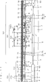
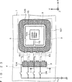
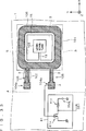
Die 10 bis 12 sind Querschnittsansichten einer Halbleitervorrichtungsstruktur nach einer zweiten bevorzugten Ausführungsform dieser Erfindung. Die 10 bis 12 sind Querschnittsansichten, die entlang der in 2 durch die Pfeile bezeichneten jeweiligen Linien A-A bis C-C genommen sind. Die Halbleitervorrichtung der zweiten bevorzugten Ausführungsform ist eine Modifikation, von der der zuvor erwähnten ersten bevorzugten Ausführungsform, die im wesentlichen ferner einen p+-vergrabenen Dotierungsbereich 50 beinhaltet.The 10 to 12 FIG. 15 are cross-sectional views of a semiconductor device structure according to a second preferred embodiment of this invention. FIG. The 10 to 12 are cross-sectional views taken along in 2 are taken by the arrows designated respective lines AA to CC. The semiconductor device of the second preferred embodiment is a modification of that of the aforementioned first preferred embodiment, which is further substantially a p + buried doping region 50 includes.
Wie in den 10 bis 12 gezeigt, ist der p+-vergrabene Dotierungsbereich 50 an der Grenzfläche zwischen der n–-Halbleiterschicht 3 und dem p–-Halbleitersubstrat 1 derart ausgebildet, daß der n+-vergrabene Dotierungsbereich 2 umgeben ist. Speziell ist der p+-vergrabene Dotierungsbereich 50 an der Grenzfläche zwischen der Peripherie der n–-Halbleiterschicht 3 und dem p–-Halbleitersubstrat 1 in dem Hochpotentialinselbereich 101 und an den Grenzflächen zwischen den n–-Halbleiterschichten 3 und dem p–-Halbleitersubstrat 1 ausgebildet, wobei die n–-Halbleiterschichten 3 sich in anderen als dem Hochpotentialinselbereich 101 befinden und jene in dem Niedrigpotentialinselbereich 104 und dem Schlitzbereich 105 beinhalten, so daß der vergrabene Dotierungsbereich Dotierungsbereich 2 umgeben ist. Anders als bei der ersten bevorzugten Ausführungsform ist der p+-Dotierungsbereich 4 derart ausgebildet, daß er den p+-vergrabenen Dotierungsbereich 50 erreicht. Die anderen Komponenten der Struktur sind identisch zu denen der Halbleitervorrichtung der ersten bevorzugten Ausführungsform und folglich wird deren Beschreibung unterlassen.As in the 10 to 12 is the p + buried dopant region 50 at the interface between the n - semiconductor layer 3 and the p - semiconductor substrate 1 formed such that the n + buried doping region 2 is surrounded. Specifically, the p + buried doping region 50 at the interface between the periphery of the n - semiconductor layer 3 and the p - semiconductor substrate 1 in the high potential island area 101 and at the interfaces between the n - semiconductor layers 3 and the p - semiconductor substrate 1 formed, wherein the n - semiconductor layers 3 in other than the high potential island area 101 and those in the low potential island area 104 and the slot area 105 include, so that the buried doping region doping region 2 is surrounded. Unlike the first preferred embodiment, the p + doping region is 4 is formed such that it has the p + buried doping region 50 reached. The other components of the structure are identical to those of the semiconductor device of the first preferred embodiment, and hence their description is omitted.
Wie oben ausgeführt, ist bei der Halbleitervorrichtung der zweiten bevorzugten Ausführungsform der p+-vergrabene Dotierungsbereich 50, der mit dem p+-Dotierungsbereich 4 verbunden ist und eine höhere Dotierungskonzentration als die n–-Halbleiterschicht 3 aufweist, an der Grenzfläche zwischen der n–-Halbleiterschicht 3 und dem p–-Halbleitersubstrats 1 in dem Schlitzbereich 105 vorgesehen. Entsprechend verursacht das Anlegen einer Umkehrspannung an einen pn-Übergang, der von dem p+-Dotierungsbereich 4, dem p+-vergrabenen Dotierungsbereich 50 und der n–-Halbleiterschicht 3 gebildet ist, daß sich Verarmungsschichten in einem großen Ausmaß in Richtung der n–-Halbleiterschicht 3 in dem Schlitzbereich 105 sowohl von dem p+-Dotierungsbereich 4, der die n–-Halbleiterschicht 3 in der Richtung der Y-Achse dazwischenliegend einschließt, sowie von dem p+-vergrabenen Dotierungsbereich 50 erstreckt. Dies verbessert die Impedanz des Kanals des JFET 102 während des Betriebs der Halbleitervorrichtung. Deshalb kann der Leckverlust der akkumulierten elektrischen Ladung in dem Urladekapazitätselement 200, wenn das Potential Vb größer als das Potential VL wird, weiter reduziert werden. As stated above, in the semiconductor device of the second preferred embodiment, the p + buried doping region is 50 that with the p + doping region 4 and a higher doping concentration than the n - semiconductor layer 3 at the interface between the n - semiconductor layer 3 and the p - semiconductor substrate 1 in the slot area 105 intended. Similarly, applying a reverse voltage to a pn junction causes the p + doping region 4 , the p + buried dopant region 50 and the n - semiconductor layer 3 is formed, that depletion layers in a large extent in the direction of the n - semiconductor layer 3 in the slot area 105 from both the p + doping region 4 , which is the n - semiconductor layer 3 in between in the direction of the Y axis and the p + buried doping region 50 extends. This improves the impedance of the channel of the JFET 102 during operation of the semiconductor device. Therefore, the leakage of the accumulated electric charge in the boot capacity element can 200 When the potential V b becomes higher than the potential V L , it can be further reduced.
Weiterhin kann der p+-Dotierungsbereich 4 der zweiten bevorzugten Ausführungsform, der derart ausgebildet ist, daß der vergrabene Dotierungsbereich Dotierungsbereich 50 erreicht wird, derart ausgebildet werden, daß er flacher diffundiert als der p+-Dotierungsbereich 4 der ersten bevorzugten Ausführungsform, der derart ausgebildet ist, daß die Grenzfläche zwischen der n–-Halbleiterschicht 3 und dem p–-Halbleitersubstrat 1 erreicht wird. Deshalb können Variationen der Breite W der n–-Halbleiterschicht 3 in dem Schlitzbereich 105 unter einer Mehrzahl von Halbleitervorrichtungen minimiert werden.Furthermore, the p + doping region 4 of the second preferred embodiment, which is formed such that the buried doping region doping region 50 is reached, be formed so that it diffuses shallower than the p + -Dotierungsbereich 4 of the first preferred embodiment, which is formed such that the interface between the n - semiconductor layer 3 and the p - semiconductor substrate 1 is reached. Therefore, variations of the width W of the n - semiconductor layer can be made 3 in the slot area 105 be minimized among a plurality of semiconductor devices.
Der Leckstrom der akkumulierten elektrischen Ladung in dem Urladekapazitätselement 200 kann auch in der zweiten bevorzugten Ausführungsform durch Setzen der Breite W der n–-Halbleiterschicht 3 in dem Schlitzbereich 105, so daß dem vorgenannten Ausdruck (1) genügt ist, weiter reduziert werden.The leakage current of the accumulated electric charge in the boot capacity element 200 can also in the second preferred embodiment by setting the width W of the n - semiconductor layer 3 in the slot area 105 so that the above expression (1) is sufficient to be further reduced.
Dritte bevorzugte AusführungsformThird preferred embodiment
13 ist eine schematische Draufsicht einer Halbleitervorrichtungsstruktur nach einer dritten bevorzugten Ausführungsform dieser Erfindung und 14 ist eine Querschnittsansicht, die entlang der durch die Pfeile in 13 bezeichneten Linie D-D genommen ist. Die Halbleitervorrichtung der dritten bevorzugten Ausführungsform ist eine Modifikation von der der vorgenannten ersten bevorzugten Ausführungsform, die eine Mehrzahl von Schlitzbereichen 105 beinhaltet. 13 FIG. 12 is a schematic plan view of a semiconductor device structure according to a third preferred embodiment of this invention and FIG 14 is a cross-sectional view taken along by the arrows in FIG 13 designated line DD is taken. The semiconductor device of the third preferred embodiment is a modification of that of the aforementioned first preferred embodiment having a plurality of slot regions 105 includes.
Wie in den 13 und 14 gezeigt, ist der p+-Dotierungsbereich 4 der dritten bevorzugten Ausführungsform derart ausgebildet, daß ein Teil der n–-Halbleiterschicht 3 umgeben ist, und definiert den Hochpotentialinselbereich 101, den Niedrigpotentialinselbereich 104 und die Mehrzahl von Schlitzbereichen 105. Jede der n–-Halbleiterschichten 3 in der Mehrzahl von Schlitzbereichen 105 ist zwischen den n–-Halbleiterschichten 3 in dem Hochpotentialinselbereich 101 und dem Niedrigpotentialinselbereich 104 angeordnet und ist mit beiden verbunden. Die weiteren Komponenten der Struktur sind identisch zu denen der Halbleitervorrichtung der ersten bevorzugten Ausführungsform und folglich wird deren Beschreibung ausgelassen.As in the 13 and 14 shown is the p + doping region 4 of the third preferred embodiment formed such that a part of the n - semiconductor layer 3 is surrounded and defines the high potential island area 101 , the low-potential island area 104 and the plurality of slot areas 105 , Each of the n - semiconductor layers 3 in the plurality of slot areas 105 is between the n - semiconductor layers 3 in the high potential island area 101 and the low potential island area 104 arranged and is connected to both. The other components of the structure are identical to those of the semiconductor device of the first preferred embodiment, and thus the description thereof is omitted.
Als solches sind in der Halbleitervorrichtung der dritten bevorzugten Ausführungsform, bei der die Mehrzahl von Schlitzbereichen 105 bereitgestellt ist, eine Mehrzahl von parasitären JFET 102 bereitgestellt. Folglich kann das Urladekapazitätselement 200 mit der Mehrzahl von parallel geschalteten JFET 102 geladen werden. Deshalb kann, selbst wenn ein ausreichender Ladestrom mit einem JFET 102 aufgrund der hohen Impedanz von dessen Kanal usw. nicht geliefert werden kann, die Mehrzahl von JFET 102 gemäß der Kapazität des Urladekapazitätselements 200 bereitgestellt sein, wodurch die Ladezeit reduziert wird.As such, in the semiconductor device of the third preferred embodiment, in which the plurality of slot regions 105 is provided, a plurality of parasitic JFET 102 provided. Consequently, the boot capacity element 200 with the plurality of JFETs connected in parallel 102 getting charged. Therefore, even if a sufficient charge current with a JFET 102 due to the high impedance of its channel, etc. can not be supplied, the plurality of JFET 102 according to the capacity of the boot capacity element 200 be provided, whereby the charging time is reduced.
Der Leckverlust der akkumulierten elektrischen Ladung in dem Urladekapazitätselement 200 kann auch in der dritten bevorzugten Ausführungsform durch Setzen der Breite W der n–-Halbleiterschicht 3 in jedem der Schlitzbereiche 105, so daß der vorgenannte Ausdruck (1) erfüllt ist, weiter reduziert werden. Es ist besonders effektiv, die Mehrzahl von JFET 102 durch Bereitstellen der Mehrzahl von Schlitzbereichen 105 wie in der dritten bevorzugten Ausführungsform zu bilden, weil in einem solchen Fall der Ladestrom zu dem Urladekapazitätselement 200 aufgrund eines Abschnüreffektes beachtlich begrenzt ist.The leakage of the accumulated electric charge in the bootstrap capacity element 200 can also in the third preferred embodiment by setting the width W of the n - semiconductor layer 3 in each of the slot areas 105 so that the aforementioned expression (1) is satisfied, further reduced. It is especially effective, the majority of JFET 102 by providing the plurality of slot areas 105 as in the third preferred embodiment, because in such a case the charge current to the bootstrap capacitance element 200 is considerably limited due to a choking effect.
Wie die der dritten bevorzugten Ausführungsform kann die Halbleitervorrichtung der zweiten bevorzugten Ausführungsform die Mehrzahl von Schlitzbereichen 105 beinhalten. 15 ist eine Querschnittsansicht in einem solchen Fall, die entlang der durch die Pfeile in 13 gezeigten Linie D-D genommen ist.Like the third preferred embodiment, the semiconductor device of the second preferred embodiment may include the plurality of slot regions 105 include. 15 is a cross-sectional view in such a case, along the arrow indicated by the arrows 13 shown line DD is taken.
Vierte bevorzugte AusführungsformFourth preferred embodiment
16 ist eine schematische Draufsicht einer Halbleitervorrichtungsstruktur nach einer vierten bevorzugten Ausführungsform dieser Erfindung und 17 ist eine Querschnittsansicht, die entlang der durch die Pfeile in 16 bezeichneten Linie E-E genommen ist. Die Halbleitervorrichtung der vierten bevorzugten Ausführungsform ist eine Modifikation von der der vorgenannten dritten bevorzugten Ausführungsform, die im wesentlichen den Niedrigpotentialinselbereich 104 in eine Mehrzahl von Bereichen unterteilt. 16 FIG. 12 is a schematic plan view of a semiconductor device structure according to a fourth preferred embodiment of this invention and FIG 17 is a cross-sectional view taken along by the arrows in FIG 16 designated line EE is taken. The semiconductor device of the fourth preferred embodiment is a modification of that of the aforementioned third preferred embodiment, which is substantially the low potential island region 104 divided into a plurality of areas.
Wie in den 16 und 17 gezeigt, ist der Niedrigpotentialinselbereich 104 der vierten bevorzugten Ausführungsform in eine Mehrzahl von geteilten Bereichen 104a unterteilt. Kurz gesagt, definiert der p+-Dotierungsbereich 4 der vierten bevorzugten Ausführungsform die Mehrzahl von geteilten Bereichen 104a in der n–-Halbleiterschicht 3. Die n–-Halbleiterschichten 3 in der Mehrzahl von geteilten Bereichen 104a sind mit den n–-Halbleiterschichten 3 in der Mehrzahl von Schlitzbereichen 105 jeweils eine mit einer verbunden. Der n+-Dotierungsbereich 6 und die Elektrode 16 sind unabhängig für jeden der geteilten Bereiche 104a bereitgestellt.As in the 16 and 17 shown is the low potential island area 104 of the fourth preferred embodiment into a plurality of divided areas 104a divided. In short, the p + doping region defines 4 According to the fourth preferred embodiment, the plurality of divided areas 104a in the n - semiconductor layer 3 , The n - semiconductor layers 3 in the majority of shared areas 104a are with the n - semiconductor layers 3 in the plurality of slot areas 105 one connected to each one. The n + doping area 6 and the electrode 16 are independent for each of the shared areas 104a provided.
Ferner ist in der Halbleitervorrichtung der vierten bevorzugten Ausführungsform eine Mehrzahl von Schalterschaltungen SW bereitgestellt. Die einen Enden der Schalterschaltungen SW sind mit der Mehrzahl von Elektroden 16 jeweils eins mit einer elektrisch verbunden und deren andere Enden mit der Spannungsquelle 150L.Further, in the semiconductor device of the fourth preferred embodiment, a plurality of switch circuits SW are provided. The one ends of the switch circuits SW are provided with the plurality of electrodes 16 one each electrically connected and their other ends connected to the voltage source 150L ,
Die Schalterschaltungen SW werden zuvor in dem An-Zustand oder dem Aus-Zustand fixiert. Durch Ausbilden der Schalterschaltungen SW mit einer Mehrzahl von zu der Mehrzahl von Elektroden 16 je einer zu einer verbundenen Elektrodenanschlüssen, den Elektrodenanschlüssen mit der Spannungsquelle 150L verbunden und sie verbindende Aluminiumverdrahtungen und durch Durchführen von Verdrahtungsverbinden oder nicht in einem Aufbauprozeß kann zum Beispiel zuvor der An-/Aus-Zustand der Schalterschaltungen SW fixiert werden.The switch circuits SW are previously fixed in the on state or the off state. By forming the switch circuits SW having a plurality of the plurality of electrodes 16 one each to a connected electrode terminals, the electrode terminals to the voltage source 150L connected and connecting aluminum wirings and by performing wiring connections or not in a building process, for example, the on / off state of the switch circuits SW can be previously fixed.
Alternativ kann der An-/Aus-Zustand der Schalterschaltungen SW zuvor durch Ausbilden der Schalterschaltungen SW mit einer Mehrzahl von mit der Mehrzahl von Elektroden 16 einer zu einer verbundenen Elektrodenanschlüssen, den Elektrodenanschlüssen mit der Spannungsquelle 150L verbunden und einer Mehrzahl von sie unabhängig verbindenden Verdrahtungen und durch Durchtrennen der Verdrahtungen oder nicht mit einem Laser oder ähnlichem in einem Aufbauprozeß fixiert werden.Alternatively, the on / off state of the switch circuits SW may be previously determined by forming the switch circuits SW having a plurality of the plurality of electrodes 16 one to a connected electrode terminals, the electrode terminals to the voltage source 150L and a plurality of wirings connecting them independently and fixed by cutting the wirings or not with a laser or the like in a building process.
Alternativ können Halbleiterschalter als die Schalterschaltungen SW angewandt werden. In diesem Fall sollte die Konfiguration derart sein, daß ein ROM in einem Wafer-Verfahren ausgebildet ist und die Halbleiterschalter durch in den ROM geschriebene Information steuerbar sind. Dann wird die An-/Aus-Information über die Halbleiterschalter in einem folgenden Testverfahren in den ROM geschrieben, wodurch der An-/Aus-Zustand von jedem der Halbleiterschalter zuvor fixiert wird. Die Schalterschaltungen SW und der ROM sind auf der vorgenannten Niedrigdurchbruchspannungsschaltung bereitgestellt. Die weiteren Komponenten der Struktur sind identisch zu denen der Halbleitervorrichtung der dritten bevorzugten Ausführungsform und folglich wird deren Beschreibung ausgelassen.Alternatively, semiconductor switches may be used as the switch circuits SW. In this case, the configuration should be such that a ROM is formed in a wafer process and the semiconductor switches are controllable by information written in the ROM. Then, the on / off information about the semiconductor switches is written in the ROM in a following test procedure, whereby the on / off state of each of the semiconductor switches is previously fixed. The switch circuits SW and the ROM are provided on the aforementioned low-breakdown voltage circuit. The other components of the structure are identical to those of the semiconductor device of the third preferred embodiment, and hence the description thereof is omitted.
Auf diese Weise gibt das Vorsehen der Schalterschaltungen SW bei der Halbleitervorrichtung der vierten bevorzugten Ausführungsform, bei der der Niedrigpotentialinselbereich 104 die Mehrzahl von geteilten Bereichen 104a enthält und die n–-Halbleiter-schichten 3 in der Mehrzahl von geteilten Bereichen 104a mit den n–-Halbleiterschichten 3 in der Mehrzahl von Schlitzbereichen 105 einer zu einer verbunden sind, eine Auswahlfreiheit unter der Mehrzahl von JFET 102, die zum Laden des Urladekapazitätselements 200 in einem Verfahren verwendet werden sollen, das einem Waferverfahren z. B. in einem Aufbauverfahren oder Testverfahren folgt. Deshalb kann eine Mehrzahl von Halbleitervorrichtungen, die die Urladekapazitätselemente 200 unterstützen, die unterschiedliche Kapazitäten aufweisen, durch Verwenden desselben Waferverfahrens hergestellt werden, wodurch die Herstellungskosten reduziert werden.In this way, the provision of the switch circuits SW in the semiconductor device of the fourth preferred embodiment gives the low-potential-island region 104 the majority of shared areas 104a contains and the n - semiconductor layers 3 in the majority of shared areas 104a with the n - semiconductor layers 3 in the plurality of slot areas 105 one to one, a freedom of choice among the plurality of JFETs 102 for loading the boot capacity element 200 to be used in a process that a wafer process z. B. in a construction process or test procedure follows. Therefore, a plurality of semiconductor devices including the boot capacitance elements 200 support having different capacities can be produced by using the same wafer process, thereby reducing the manufacturing cost.
Fünfte bevorzugte AusführungsformFifth Preferred Embodiment
18 ist eine schematische Draufsicht einer Halbleitervorrichtungsstruktur nach einer fünften bevorzugten Ausführungsform dieser Erfindung. Die 19 bis 21 sind Querschnittsansichten, die entlang jeweiligen durch die Pfeile in 18 gekennzeichneten Linien F-F bis H-H genommen sind. Die Halbleitervorrichtung der fünften bevorzugten Ausführungsform ist eine Modifikation von der der vorgenannten ersten bevorzugten Ausführungsform, die im wesentlichen ferner eine Gateelektrode 60 und eine Gateisolierschicht 61 beinhaltet. 18 FIG. 12 is a schematic plan view of a semiconductor device structure according to a fifth preferred embodiment of this invention. FIG. The 19 to 21 are cross-sectional views taken respectively through the arrows in FIG 18 marked lines FF to HH are taken. The semiconductor device of the fifth preferred embodiment is a modification of that of the aforementioned first preferred embodiment, which is also substantially a gate electrode 60 and a gate insulating layer 61 includes.
Wie in den 18 bis 21 gezeigt, ist die Gateisolierschicht 61, die viel dünner als die Oxidschicht 12 ist, anstelle der Oxidschicht 12 auf der n–-Halbleiterschicht 3 in dem Schlitzbereich 105 vorgesehen und die Gateelektrode 60 ist darauf bereitgestellt. Die Gateelektrode 60 ist auch teilweise über die Oxidschicht 12 auf dem die n–-Halbleiterschicht 3 in dem Schlitzbereich 105 in der Richtung der Y-Achse dazwischenliegend einschließenden p+-Dotierungsbereich 4 vorgesehen.As in the 18 to 21 is the gate insulating layer 61 that is much thinner than the oxide layer 12 is, instead of the oxide layer 12 on the n - semiconductor layer 3 in the slot area 105 provided and the gate electrode 60 is provided thereon. The gate electrode 60 is also partially over the oxide layer 12 on the the n - semiconductor layer 3 in the slot area 105 in the direction of the Y-axis intervening p + -type doping region 4 intended.
Die Gateelektrode 60 ist zum Beispiel eine aus Polysilizium bestehende leitende Schicht. Die Gateisolierschicht 61 besteht zum Beispiel aus einer Siliziumoxidschicht. Die weiteren Komponenten der Struktur sind identisch zu jenen der Halbleitervorrichtung der ersten bevorzugten Ausführungsform und folglich wird deren Beschreibung ausgelassen.The gate electrode 60 is, for example, a conductive layer made of polysilicon. The gate insulating layer 61 For example, it consists of a silicon oxide layer. The other components of the structure are identical to those of the semiconductor device of the first preferred embodiment, and hence the description thereof is omitted.
In dieser Weise führt bei der Halbleitervorrichtung der fünften bevorzugten Ausführungsform, bei der die Gateelektrode 60 über die Gateisolierschicht 61 auf der n–-Halbleiterschicht 3 in dem Schlitzbereich 105 vorgesehen ist, das Anwenden eines positiven Potentials auf die Gateelektrode 60 zu dem Ausbilden einer Akkumulationsschicht in der Nähe der oberen Oberfläche der n–-Halbleiterschicht 3 in dem Schlitzbereich 105. Dies verbessert die Mobilität der Elektronen in dem Kanal des JFET 102. Folglich steigt der Ladestrom zu dem Urladekapazitätselement 200, sodaß das Laden in einer kurzen Zeit komplettiert wird. In this way, in the semiconductor device of the fifth preferred embodiment, in which the gate electrode 60 over the gate insulating layer 61 on the n - semiconductor layer 3 in the slot area 105 is provided applying a positive potential to the gate electrode 60 for forming an accumulation layer near the upper surface of the n - semiconductor layer 3 in the slot area 105 , This improves the mobility of the electrons in the channel of the JFET 102 , Consequently, the charging current to the boot capacity element increases 200 , so that the loading will be completed in a short time.
Wenn ein Anlegepotential Vg zu der Gateelektrode 60 ansteigt, wird die Mobilität von Elektronen in der n–-Halbleiterschicht 3 in dem Schlitzbereich 105 verbessert, wodurch der Anfangsladestrom ansteigt. Kurz gesagt ist der Anfangsladestrom durch das an die Gateelektrode 60 angelegte Potential Vg steuerbar. 22 zeigt die Beziehung zwischen dem Anlegepotential Vg und dem Anfangsladestrom und erklärt, daß der Anfangsladestrom ansteigt, wenn das Potential Vg zu der Gateelektrode 60 ansteigt.When an application potential V g to the gate electrode 60 increases, the mobility of electrons in the n - semiconductor layer 3 in the slot area 105 improves, whereby the initial charging current increases. In short, the initial charging current is through that to the gate electrode 60 applied potential V g controllable. 22 FIG. 12 shows the relationship between the application potential V g and the initial charging current, and explains that the initial charging current increases when the potential V g to the gate electrode 60 increases.
Wenn das Laden zu dem Urladekapazitätselement 200 komplettiert ist und das Potential VS auf das Potential VH gesetzt ist, kann der Leckverlust der angesammelten elektrischen Ladung in dem Urladekapazitätselement 200 durch Anlegen eines Massepotentials an die Gateelektrode 60 reduziert werden. Während die Gateelektrode 60 auch teilweise über die Oxidschicht 12 auf dem p+-Dotierungsbereich 4 vorgesehen ist, ist es möglich durch Einstellen der Dicke der Oxidschicht 12 zu verhindern, daß eine Inversionsschicht in der Nähe der Oberfläche des p+-Dotierungsbereich 4 ausgebildet wird.When loading to the boot capacity element 200 is completed and the potential V S is set to the potential V H , the leakage of the accumulated electric charge in the boot capacity element 200 by applying a ground potential to the gate electrode 60 be reduced. While the gate electrode 60 also partially over the oxide layer 12 on the p + doping region 4 is provided, it is possible by adjusting the thickness of the oxide layer 12 to prevent an inversion layer near the surface of the p + doping region 4 is trained.
Die Halbleitervorrichtungen der vorgenannten dritten und vierten bevorzugten Ausführungsform können ebenfalls durch Ausbilden der Gateisolierschicht 61 auf den n–-Halbleiterschichten 3 in der Mehrzahl von Schlitzbereichen 105, Vorsehen der Gateelektrode 60 gemeinsam für die Mehrzahl von Schlitzbereichen 105 auf den Gateisolierschichten 61 und Anlegen eines positiven Potentials an die Gateelektrode 60 die Mobilität der Elektronen in dem Kanal von jedem JFET 102 verbessern, so daß ähnliche Effekte zu der Halbleitervorrichtung der fünften bevorzugten Ausführungsform erzeugt werden.The semiconductor devices of the aforementioned third and fourth preferred embodiments may also be formed by forming the gate insulating film 61 on the n - semiconductor layers 3 in the plurality of slot areas 105 , Provide the gate electrode 60 together for the plurality of slot areas 105 on the gate insulating layers 61 and applying a positive potential to the gate electrode 60 the mobility of the electrons in the channel of each JFET 102 so that similar effects are produced to the semiconductor device of the fifth preferred embodiment.
Sechste bevorzugte AusführungsformSixth preferred embodiment
23 ist eine schematische Draufsicht einer Halbleitervorrichtungsstruktur nach einer sechsten bevorzugten Ausführungsform dieser Erfindung. 24 ist eine Querschnittsansicht, die entlang der durch die Pfeile in 23 bezeichneten Linie I-I genommen ist. Die Halbleitervorrichtung der sechsten bevorzugten Ausführungsform ist eine Modifikation von der der vorgenannten dritten bevorzugten Ausführungsform, die im wesentlichen die Gateelektrode 60 und die Gateisolierschicht 61 für jeden der Schlitzbereiche 105 beinhaltet. 23 FIG. 12 is a schematic plan view of a semiconductor device structure according to a sixth preferred embodiment of this invention. FIG. 24 is a cross-sectional view taken along by the arrows in FIG 23 designated line II is taken. The semiconductor device of the sixth preferred embodiment is a modification of that of the aforementioned third preferred embodiment, which is substantially the gate electrode 60 and the gate insulating layer 61 for each of the slot areas 105 includes.
Wie in den 23 und 24 gezeigt, sind Gateisolierschichten 61 voneinander getrennt auf den jeweiligen n–-Halbleiterschichten 3 in der Mehrzahl von Schlitzbereichen 105 vorgesehen und die Gateelektroden 60 sind voneinander getrennt auf den jeweiligen Gateisolierschichten 61 vorgesehen. Kurz gesagt sind die Gateelektroden 60 jeweils eine für eine entsprechend für die n–-Halb-leiterschichten 3 in der Mehrzahl von Schlitzbereichen 105 vorgesehen.As in the 23 and 24 Shown are gate insulating layers 61 separated from each other on the respective n - semiconductor layers 3 in the plurality of slot areas 105 provided and the gate electrodes 60 are separated from each other on the respective gate insulating layers 61 intended. In short, the gate electrodes 60 one for a corresponding one for the n - half semiconductor layers 3 in the plurality of slot areas 105 intended.
Die Halbleitervorrichtung der sechsten bevorzugten Ausführungsform beinhaltet ferner die vorgenannte Mehrzahl von Schalterschaltungen SW, deren eine Enden elektrisch mit der Mehrzahl von Gateelektroden 60 je eines zu einer verbunden sind und deren andere Enden mit der Spannungsquelle 150L verbunden sind. Wie bei der vierten bevorzugten Ausführungsform wird in einem Verfahren, das einem Waferverfahren folgt, z. B. in einem Aufbauverfahren oder Testverfahren, für die Mehrzahl von Schalterschaltungen SW der sechsten bevorzugten Ausführungsform unabhängig bestimmt, ob sie in dem An-Zustand oder dem Aus-Zustand sein sollen.The semiconductor device of the sixth preferred embodiment further includes the aforementioned plurality of switch circuits SW having one ends electrically connected to the plurality of gate electrodes 60 one connected to one and the other ends connected to the voltage source 150L are connected. As in the fourth preferred embodiment, in a process following a wafer process, e.g. In a setup method or test method, for the plurality of switch circuits SW of the sixth preferred embodiment, independently determines whether they should be in the on state or the off state.
Auf diese Weise gibt bei der Halbleitervorrichtung der sechsten bevorzugten Ausführungsform, bei der die Gateelektroden 60 unabhängig durch die Gateisolierschichten 61 auf den jeweiligen n–-Halbleiterschichten 3 in der Mehrzahl von Schlitzbereichen 105 bereitgestellt sind, das Vorsehen der vorgenannten Schalterschaltungen SW in einem Verfahren, das einem Waferverfahren folgt, z. B. in einem Aufbauverfahren oder Testverfahren, die Auswahlfreiheit unter den n–-Halbleiterschichten 3 in der Mehrzahl von Schlitzbereichen 105, wo eine Akkumulationsschicht ausgebildet werden soll. Kurz gesagt kann nach einem Waferverfahren eine Entscheidung getroffen werden, in welchem JFET 102 unter der Mehrzahl von JFET 102 die Mobilität der Elektronen in dem Kanal verbessert wird. Deshalb kann eine Mehrzahl von Halbleitervorrichtungen, die die Urladekapazitätselemente 200 unterstützen, die unterschiedliche Kapazitäten aufweisen, durch Verwenden desselben Waferprozesses hergestellt werden, wodurch Herstellungskosten reduziert werden.In this way, in the semiconductor device of the sixth preferred embodiment, the gate electrodes 60 independently through the gate insulating layers 61 on the respective n - semiconductor layers 3 in the plurality of slot areas 105 are provided, the provision of the aforementioned switch circuits SW in a process following a wafer process, for. In a build-up process or test procedure, freedom of choice among the n - semiconductor layers 3 in the plurality of slot areas 105 where an accumulation layer is to be formed. In short, after a wafer process, a decision can be made in which JFET 102 among the majority of JFETs 102 the mobility of the electrons in the channel is improved. Therefore, a plurality of semiconductor devices including the boot capacitance elements 200 support having different capacities can be produced by using the same wafer process, thereby reducing manufacturing costs.
Siebte bevorzugte AusführungsformSeventh Preferred Embodiment
25 ist eine schematische Draufsicht einer Halbleitervorrichtungsstruktur nach einer siebten bevorzugten Ausführungsform dieser Erfindung. Die 26 bis 28 sind Querschnittsansichten, die entlang jeweiligen in 25 durch die Pfeile bezeichneten Linien J-J bis L-L genommen sind. Die Halbleitervorrichtung der siebten bevorzugten Ausführungsform ist eine Modifikation von der der vorgenannten ersten bevorzugten Ausführungsform, die einen p+-Dotierungsbereich 70 anstelle des n+-Dotierungsbereichs 6 beinhaltet und ferner einen n+-vergrabenen Dotierungsbereich 71 beinhaltet. 25 FIG. 12 is a schematic plan view of a semiconductor device structure according to a seventh preferred embodiment of this invention. FIG. The 26 to 28 are cross-sectional views taken along respective ones in FIG 25 lines JJ through LL are taken. The Semiconductor device of the seventh preferred embodiment is a modification of that of the aforementioned first preferred embodiment, the p + doping region 70 instead of the n + doping area 6 and further includes an n + buried doping region 71 includes.
Wie in den 25 bis 28 gezeigt, ist der p+-Dotierungsbereich 70 getrennt von dem p+-Dotierungsbereich 4 in der oberen Oberfläche der n–-Halbleiterschicht 3 in dem Niedrigpotentialinselbereich 104 vorgesehen. Die Elektrode 16 ist mit dem p+-Dotierungsbereich 70 verbunden. Der n+-vergrabene Dotierungsbereich 71 ist an der Grenzfläche zwischen der n–-Halbleiterschicht 3 und dem p–-Halbleitersubstrat 1 in dem Niedrigpotentialinselbereich 104 unterhalb des p+-Dotierungsbereichs 70 vorgesehen. Die weiteren Komponenten der Struktur sind identisch zu jenen der Halbleitervorrichtung der ersten bevorzugten Ausführungsform und folglich wird deren Beschreibung ausgelassen.As in the 25 to 28 shown is the p + doping region 70 separated from the p + doping region 4 in the upper surface of the n - semiconductor layer 3 in the low potential island area 104 intended. The electrode 16 is with the p + doping region 70 connected. The n + buried doping region 71 is at the interface between the n - semiconductor layer 3 and the p - semiconductor substrate 1 in the low potential island area 104 below the p + doping region 70 intended. The other components of the structure are identical to those of the semiconductor device of the first preferred embodiment, and hence the description thereof is omitted.
Wie oben diskutiert, ist bei der Halbleitervorrichtung der siebten bevorzugten Ausführungsform der p+-Dotierungsbereich 70 mit der Elektrode 16 verbunden, an die das Potential VL anliegt, in der oberen Oberfläche der n–-Halbleiterschicht 3 in dem Niedrigpotentialinselbereich 104 vorgesehen. Folglich bilden der p+-Dotierungsbereich 70 und die damit in Kontakt stehende n–-Halbleiterschicht 3 eine pn-Übergang-Diode.As discussed above, in the semiconductor device of the seventh preferred embodiment, the p + -type impurity region 70 with the electrode 16 connected to which the potential V L is applied, in the upper surface of the n - semiconductor layer 3 in the low potential island area 104 intended. Consequently, the p + doping region forms 70 and the n -type semiconductor layer in contact therewith 3 a pn-junction diode.
29 zeigt eine äquivalente Schaltung der Halbleitervorrichtung der siebten bevorzugten Ausführungsform. Wie in 29 gezeigt, bedeutet das Vorsehen des p+-Dotierungsbereichs 70 das äquivalente Einsetzen einer Diode 110 zwischen dem Drain des JFET 102 und der Spannungsquelle 150L, so daß der Ladestrom zu dem Urladekapazitätselement 200 durch die Diode 110 und den JFET 102 geliefert wird. Kurz gesagt geht der von der Spannungsquelle 150L gelieferte Ladestrom durch den p+-Dotierungsbereich 70, der ein Anodenbereich der Diode 110 ist, die n–-Halbleiterschicht 3 in dem Schlitzbereich 105 und die n–-Halbleiterschicht 3 in dem Hochpotentialinselbereich 101 in dieser Reihenfolge, so daß er zu dem Urladekapazitätselement 200 geliefert wird. 29 shows an equivalent circuit of the semiconductor device of the seventh preferred embodiment. As in 29 shows the provision of the p + doping region 70 the equivalent insertion of a diode 110 between the drain of the JFET 102 and the voltage source 150L such that the charging current to the bootstrap capacity element 200 through the diode 110 and the JFET 102 is delivered. In short, it goes from the voltage source 150L supplied charging current through the p + -Dotierungsbereich 70 , which is an anode region of the diode 110 is, the n - semiconductor layer 3 in the slot area 105 and the n - semiconductor layer 3 in the high potential island area 101 in that order, so that it belongs to the boot capacity element 200 is delivered.
Bei der Halbleitervorrichtung der siebten bevorzugten Ausführungsform, bei der der Ladestrom zu dem Urladekapazitätselement 200 durch die Diode geliefert wird, die von dem p+-Dotierungsbereich 70 und der damit in Kontakt stehenden n–-Halbleiterschicht 3 gebildet ist, kann auf diese Weise der Leckverlust der akkumulierten elektrischen Ladung in dem Urladekapazitätselement 200 reduziert werden, selbst wenn nachdem das Laden komplettiert ist, das Potential Vb größer als das Potential VL wird.In the semiconductor device of the seventh preferred embodiment, in which the charging current to the bootstrap capacitance element 200 is supplied by the diode, that of the p + -doping region 70 and the n - semiconductor layer in contact therewith 3 can be formed in this way, the leakage of the accumulated electric charge in the bootstrap capacity element 200 can be reduced, even after the charging is completed, the potential V b becomes larger than the potential V L.
Bei der Halbleitervorrichtung der siebten bevorzugten Ausführungsform, bei der der n+-vergrabene Dotierungsbereich 71 mit einer höheren Dotierungskonzentration als die n–-Halbleiterschicht 3 vorgesehen ist, kann weiterhin der durch einen in der Halbleitervorrichtung gebildeten parasitären Bipolartransistor verursachte Leckverlust reduziert werden. Dies wird unten im Detail erklärt.In the semiconductor device of the seventh preferred embodiment, wherein the n + buried doping region 71 with a higher doping concentration than the n - semiconductor layer 3 is provided, further, the leakage caused by a parasitic bipolar transistor formed in the semiconductor device can be reduced. This will be explained in detail below.
30 zeigt den in der Halbleitervorrichtung der siebten bevorzugten Ausführungsform gebildeten parasitären Bipolartransistor und ist eine Querschnittsansicht entlang der durch die Pfeile in 25 bezeichneten Linie L-L. Aus Gründen der Einfachheit sind in 30 die Elektrode 16 und die Isolierschichten 8 und 18 nicht gezeigt. 30 FIG. 12 shows the parasitic bipolar transistor formed in the semiconductor device of the seventh preferred embodiment, and FIG. 12 is a cross-sectional view taken along the direction indicated by arrows in FIG 25 designated line LL. For the sake of simplicity are in 30 the electrode 16 and the insulating layers 8th and 18 Not shown.
Wie in 30 gezeigt, bilden der p+-Dotierungsbereich 4, die n–-Halbleiterschicht 3 und der p+-Dotierungsbereich 70 einen parasitären pnp-Bipolartransistor 160. Währenddessen bilden das p–-Halbleitersubstrat 1, die n–-Halbleiterschicht 3, der n+-vergrabene Dotierungsbereich 71 und der p+-Dotierungsbereich 70 einen parasitären pnp-Bipolartransistor 161. Die Transistoren 160 und 161 sind parallel geschaltet.As in 30 shown form the p + doping region 4 , the n - semiconductor layer 3 and the p + doping region 70 a parasitic pnp bipolar transistor 160 , Meanwhile, the p - semiconductor substrate is formed 1 , the n - semiconductor layer 3 , the n + buried doping region 71 and the p + doping region 70 a parasitic pnp bipolar transistor 161 , The transistors 160 and 161 are connected in parallel.
Bei der Halbleitervorrichtung der siebten bevorzugten Ausführungsform, bei der die obigen parasitären pnp-Bipolartransistoren 160 und 161 ausgebildet sind, wird, wenn die Transistoren 160 und 161 zum Laden des Urladekapazitätselements 200 arbeiten, ein Teil des von der Spannungsquelle 150L gelieferten Ladestroms zu Kollektorströmen der Transistoren und entweicht in Richtung des p–-Halbleitersubstrats 1, das auf ein Massepotential gesetzt ist. Deshalb müssen die Stromverstärkungsfaktoren hFE der Transistoren 160 und 161 reduziert werden, um den Leckverlust des Ladestroms zu unterdrücken.In the semiconductor device of the seventh preferred embodiment, in which the above parasitic pnp bipolar transistors 160 and 161 are formed, when the transistors 160 and 161 for loading the boot capacity element 200 work, part of the voltage source 150L supplied charging current to collector currents of the transistors and escapes in the direction of the p - -Halbleitersubstrats 1 which is set to a ground potential. Therefore, the current gain factors must h FE of the transistors 160 and 161 be reduced to suppress the leakage of the charging current.
Bei der siebten bevorzugten Ausführungsform, bei der der n+-vergrabene Dotierungsbereich 71 an der Grenzfläche zwischen der n–-Halbleiterschicht 3 und dem p–-Halbleitersubstrat 1 in dem Niedrigpotentialinselbereich 104 unterhalb des p+-Dotierungsbereichs 70 vorgesehen ist, steigt die Dotierungskonzentration eines Basisbereiches des parasitären pnp-Bipolartransistors 161 höher an, als wenn der Bereich 71 nicht vorgesehen ist. Dies reduziert den Stromverstärkungsfaktor hFE des Transistors 161, wodurch der Leckverlust des Ladestroms unterdrückt wird.In the seventh preferred embodiment, wherein the n + buried doping region 71 at the interface between the n - semiconductor layer 3 and the p - semiconductor substrate 1 in the low potential island area 104 below the p + doping region 70 is provided, the doping concentration of a base region of the parasitic pnp bipolar transistor increases 161 higher than if the range 71 is not provided. This reduces the current amplification factor h FE of the transistor 161 , whereby the leakage of the charging current is suppressed.
Andererseits kann der Stromverstärkungsfaktor hFE des parasitären pnp-Bipolartransistors 160 durch Vergrößern eines Abstandes L zwischen dem p+-Dotierungsbereich 4 und dem p+-Dotierungsbereich 70 reduziert werden, wie in 28 gezeigt.On the other hand, the current amplification factor h FE of the parasitic pnp bipolar transistor 160 by increasing a distance L between the p + doping region 4 and the p + doping region 70 be reduced, as in 28 shown.
Bei der siebten bevorzugten Ausführungsform verhindert das Vorsehen des n+-vergrabenen Dotierungsbereichs 71 das Ausbreiten einer Verarmungsschicht in der n–-Halbleiterschicht 3 in dem Niedrigpotentialinselbereich 104. Die n–-Halbleiterschichten 3 in dem Niedrigpotentialinselbereich 104 und dem Hochpotentialinselbereich 101 sind jedoch zwar nicht direkt aber doch durch die n–-Halbleiterschicht 3 in dem Schlitzbereich 105 verbunden. Diese n–-Halbleiterschicht 3 in dem Schlitzbereich 105 kann leicht verarmt werden, weil deren Breite W derart gesetzt ist, daß sie geringer als die Breite HW der n–-Halbleiterschicht 3 in dem Hochpotentialinselbereich 101 ist. Dementsprechend kann die Logikschaltung 103 aufgrund des RESURF-Effektes zuverlässig von der Verarmungsschicht umgeben werden, wodurch eine durch das Vorsehen des n+-vergrabenen Dotierungsbereichs 7 verursachte Reduktion der Durchbruchsspannung reduziert wird.In the seventh preferred embodiment, the provision of the n + buried prevents dopant region 71 the spreading of a depletion layer in the n - semiconductor layer 3 in the low potential island area 104 , The n - semiconductor layers 3 in the low potential island area 104 and the high potential island area 101 although not directly but through the n - semiconductor layer 3 in the slot area 105 connected. This n - semiconductor layer 3 in the slot area 105 can be easily depleted because its width W is set to be smaller than the width HW of the n - semiconductor layer 3 in the high potential island area 101 is. Accordingly, the logic circuit 103 due to the RESURF effect, be reliably surrounded by the depletion layer, thereby providing a doping region buried by the provision of the n + -type 7 caused reduction of the breakdown voltage is reduced.
Achte bevorzugte AusführungsformEighth preferred embodiment
31 ist eine schematische Draufsicht einer Halbleitervorrichtungsstruktur nach einer achten bevorzugten Ausführungsform dieser Erfindung. Die Halbleitervorrichtung der achten bevorzugten Ausführungsform ist eine Modifikation von der der vorgenannten vierten bevorzugten Ausführungsform, die im wesentlichen nur zwei Paare, von denen jedes aus dem Schlitzbereich 105 und dem geteilten Bereich 104a besteht, und eine Detektionsschaltung 80 anstelle der Schalterschaltungen SW beinhaltet, die elektrisch mit der n–-Halbleiterschicht 3 in dem geteilten Bereich 104a eines Paares verbunden ist. 31 FIG. 12 is a schematic plan view of a semiconductor device structure according to an eighth preferred embodiment of this invention. FIG. The semiconductor device of the eighth preferred embodiment is a modification of that of the aforementioned fourth preferred embodiment, which is substantially only two pairs each of which is out of the slot region 105 and the shared area 104a consists, and a detection circuit 80 instead of the switch circuits SW which is electrically connected to the n - semiconductor layer 3 in the shared area 104a of a couple is connected.
Wie in 31 gezeigt, sind bei der achten bevorzugten Ausführungsform zwei Schlitzbereiche 105 und zwei geteilte Bereiche 104a bereitgestellt und die n–-Halbleiterschichten 3 in den geteilten Bereichen 104a und die n–-Halbleiterschichten 3 in den Schlitzbereichen 105 sind jeweils eine zu einer verbunden. Der n+-Dotierungsbereich 6 und die Elektrode 16 sind unabhängig für jeden der geteilten Bereiche 104a bereitgestellt.As in 31 are shown in the eighth preferred embodiment, two slot areas 105 and two shared areas 104a provided and the n - semiconductor layers 3 in the divided areas 104a and the n - semiconductor layers 3 in the slot areas 105 each one is connected to one. The n + doping area 6 and the electrode 16 are independent for each of the shared areas 104a provided.
Bei der achten bevorzugten Ausführungsform wird das Ausgangspotential VL an der Spannungsquelle 150L an die n–-Halbleiterschicht 3 in einem der zwei geteilten Bereiche 104a durch die Elektrode 16 und den n+-Dotierungsbereich 6 angelegt, während die Detektionsschaltung 80 elektrisch mit der n–-Halbleiterschicht 3 in dem anderen geteilten Bereich 104a verbunden ist. Der eine und der andere geteilte Bereich 104a werden im weiteren als ”geteilter Bereich 104aa” bzw. ”geteilter Bereich 104ab” bezeichnet. Ferner wird der eine der Schlitzbereiche 105, der mit dem geteilten Bereich 104aa gepaart ist, als ein ”Schlitzbereich 105aa” bezeichnet und der andere mit dem geteilten Bereich 104ab gepaarte Schlitzbereich 105 als ein ”Schlitzbereich 105ab”.In the eighth preferred embodiment, the output potential V L becomes the voltage source 150L to the n - semiconductor layer 3 in one of the two shared areas 104a through the electrode 16 and the n + doping region 6 created while the detection circuit 80 electrically with the n - semiconductor layer 3 in the other shared area 104a connected is. One and the other shared area 104a will be referred to as "shared area 104aa "Or" split range 104ab " designated. Further, the one of the slot areas becomes 105 that with the shared area 104aa paired as a "slot area 105aa "And the other with the shared area 104ab paired slot area 105 as a "slot area 105ab ".
Die Detektionsschaltung 80 detektiert ein Potential V0 an der n–-Halbleiterschicht 3 in dem geteilten Bereich 104ab und ist in der vorgenannten Niedrigdurchbruchspannungsschaltung vorgesehen. Die Detektionsschaltung 80 beinhaltet einen p-Kanal MOSFET 80p vom Anreicherungstyp, einen n-Kanal MOSFET 80n vom Anreicherungstyp und eine Schutzdiode 80d und als dessen positives Leistungsversorgungspotential ist das Potential VL angelegt.The detection circuit 80 detects a potential V0 on the n - semiconductor layer 3 in the shared area 104ab and is provided in the aforementioned low-breakdown voltage circuit. The detection circuit 80 includes a p-channel MOSFET 80p of the enhancement type, an n-channel MOSFET 80n of the enrichment type and a protection diode 80d and as its positive power supply potential, the potential V L is applied.
Der p-Kanal MOSFET 80p und der n-Kanal MOSFET 80n bilden einen CMOS-Invertierer 80pn und das Potential VL und ein Massepotential sind an die Source des p-Kanal MOSFET 80p bzw. des n-Kanal MOSFET 80n angelegt. Die Gates des p-Kanal MOSFET 80p und des n-Kanal MOSFET 80n sind elektrisch mit der n–-Halbleiterschicht 3 in dem geteilten Bereich 104ab und ferner mit der Kathode der Schutzdiode 80d verbunden. Ein Massepotential liegt an der Anode der Schutzdiode 80d an. Die Detektionsschaltung 80 gibt das Ausgangspotential an dem CMOS-Invertierer 80pn, d. h. das Potential an den Drains des p-Kanal MOSFET 80p und des n-Kanal MOSFET 80n, die miteinander verbunden sind, als ein Detektionssignal DS0 aus.The p-channel MOSFET 80p and the n-channel MOSFET 80n form a CMOS inverter 80pn and the potential V L and a ground potential are at the source of the p-channel MOSFET 80p or the n-channel MOSFET 80n created. The gates of the p-channel MOSFET 80p and the n-channel MOSFET 80n are electrically connected to the n - semiconductor layer 3 in the shared area 104ab and further to the cathode of the protection diode 80d connected. A ground potential is at the anode of the protection diode 80d at. The detection circuit 80 gives the output potential at the CMOS inverter 80pn ie the potential at the drains of the p-channel MOSFET 80p and the n-channel MOSFET 80n which are connected to each other as a detection signal DS0.
Die Detektionsschaltung 80 mit der obigen Struktur gibt das Detektionssignal DS0 eines hohen Pegels aus, wenn das Potential V0 an der n–-Halbleiterschicht 3 in dem geteilten Bereich 104ab niedriger als ein Schwellenpotential Vth0 an dem CMOS-Invertierer 80pn ist, und gibt das Detektionssignal DS0 eines niedrigen Pegels aus, wenn das Potential V0 das Schwellenpotential Vth0 übersteigt.The detection circuit 80 With the above structure, the detection signal DS0 outputs high level when the potential V0 at the n - semiconductor layer 3 in the shared area 104ab lower than a threshold potential V th0 at the CMOS inverter 80pn is, and outputs the detection signal DS0 of a low level when the potential V0 exceeds the threshold potential V th0 .
Bei der achten bevorzugten Ausführungsform kann das Potential an der n–-Halbleiterschicht 3 in dem Hochpotentialinselbereich 101, d. h. das Potential Vb, indirekt durch Detektieren des Potentials V0 mit der Detektionsschaltung 80 detektiert werden. Dies wird unten im Detail erklärt.In the eighth preferred embodiment, the potential at the n - semiconductor layer 3 in the high potential island area 101 , ie the potential V b , indirectly by detecting the potential V0 with the detection circuit 80 be detected. This will be explained in detail below.
Die 32A bis 32C zeigen Potentialsignalverläufe des Potentials Vb, des Potentials V0 bzw. des Detektionssignals DS0, 32A das Potential Vb anzeigend, 32B das Potential V0 anzeigend und 32C das Detektionssignal DS0 anzeigend. Wenn das Potential VL an die n–-Halbleiterschicht 3 in dem geteilten Bereich 104aa angelegt wird, um das Laden des Urladekapazitätselements 200 zu beginnen, steigt, wie in 32A gezeigt, das Potential Vb an. Mit dem Ansteigen des Potentials Vb wird das Potential V0, das als in einem schwebenden Zustand betrachtet werden kann, durch das Potential Vb induziert und steigt an, wie in 32B gezeigt. Dann steigt mit dem Ansteigen in den Potentialen Vb und V0 die Proportion einer Verarmungsschicht in der n–-Halbleiterschicht 3 in dem geteilten Bereich 104ab an.The 32A to 32C show potential signal waveforms of the potential V b , the potential V0 and the detection signal DS0, 32A indicating the potential V b , 32B indicating the potential V0 and 32C indicating the detection signal DS0. When the potential V L to the n - semiconductor layer 3 in the shared area 104aa is created to load the boot capacity element 200 to begin, as in 32A shown, the potential V b . With the increase of the potential V b , the potential V0, which can be regarded as being in a floating state, is induced by the potential V b and rises, as in FIG 32B shown. Then, as the potentials V b and V 0 increase, the proportion of a depletion layer in the n - semiconductor layer increases 3 in the shared area 104ab at.
Wenn das Laden zu dem Urladekapazitätselement 200 vervollständigt ist und Vb auf VL ansteigt, wird das Ausgangspotential VS an der virtuellen Spannungsquelle 150H auf das Potential VH gesetzt, wodurch das Potential Vb auf (VL + VH) ansteigt. Zu dieser Zeit steigt das Potential V0 dort, wo die n–-Halbleiterschicht 3 in dem geteilten Bereich 104ab komplett mit der Verarmungsschicht bedeckt ist, nur auf ein Potential VF an, das auf einige zig Volt gesetzt ist. Folglich steigt das Potential V0 nicht höher als einige zig Volt an. Der Wert des Potentials VF kann durch Variieren der Breite W der n–-Halbleiterschicht 3 in dem Schlitzbereich 1058ab eingestellt werden. Beispielsweise ist das Potential VF durch Setzen der Breite W, so daß der vorgenannte Ausdruck (1) erfüllt ist, auf einige zig Volt gesetzt. When loading to the boot capacity element 200 is completed and V b rises to V L , the output potential V s at the virtual power source 150H is set to the potential V H , whereby the potential V b rises to (V L + V H ). At this time, the potential V0 rises where the n - semiconductor layer 3 in the shared area 104ab is completely covered with the depletion layer, only to a potential V F , which is set to several tens of volts. Consequently, the potential V0 does not rise higher than several tens of volts. The value of the potential V F can be obtained by varying the width W of the n - semiconductor layer 3 in the slot area 1058ab be set. For example, by setting the width W so as to satisfy the aforementioned expression (1), the potential V F is set to several tens of volts.
Auf diese Weise steigt bei der achten bevorzugten Ausführungsform das Potential V0 an, wenn das Potential Vb ansteigt und steigt nicht höher als einige zig Volt an, selbst wenn das Potential Vb einige hundert Volt wird. Deshalb kann das Potential V0 mit einer Schaltung wie der Detektionsschaltung 80, die mit einer Leistungsversorgung von einigen zig Volt arbeitet, detektiert werden.In this way, in the eighth preferred embodiment, the potential V0 increases as the potential increases and V b does not rise higher than a few tens of volts, even if the potential V b is a few hundred volts. Therefore, the potential V0 may be connected to a circuit such as the detection circuit 80 , which works with a power supply of a few tens of volts, can be detected.
Bei der Detektionsschaltung 80 ist das Schwellenpotential Vth0 an dem CMOS-Invertierer 80pn derart gesetzt, daß es niedriger als das Potential VF ist. Dementsprechend gibt, wie in 32C gezeigt, die Detektionsschaltung 80 zu Beginn des Ladens des Urladekapazitätselements 200 das Detektionssignal DS0 eines niedrigen Pegels aus und gibt das Detektionssignal DS0 eines niedrigen Pegels aus, wenn das Laden komplettiert ist und das Potential Vb ein hohes Potential wird.In the detection circuit 80 is the threshold potential V th0 at the CMOS inverter 80pn set so that it is lower than the potential V F. Accordingly, as in 32C shown the detection circuit 80 at the beginning of the loading of the boot capacity element 200 the detection signal DS0 of a low level and outputs the detection signal DS0 of a low level when the loading is completed and the potential V b becomes a high potential.
Auf diese Weise können bei der Halbleitervorrichtung der achten bevorzugten Ausführungsform, bei der das Potential V0 an der n–-Halbleiterschicht 3 in dem geteilten Bereich 104ab mit einem Ansteigen in dem Potential Vb ansteigt, Beobachtungen der Potentialvariationen in der n–-Halbleiterschicht 3 in dem Hochpotentialinselbereich 101 durch Detektieren des Potentials V0 gemacht werden.In this way, in the semiconductor device of the eighth preferred embodiment, the potential V0 can be applied to the n - semiconductor layer 3 in the shared area 104ab increases with an increase in the potential V b , observations of the potential variations in the n - semiconductor layer 3 in the high potential island area 101 be made by detecting the potential V0.
Weil das Potential V0 aufhört anzusteigen, nachdem die Potentiale Vb und V0 ansteigen, so daß die n–-Halbleiterschicht 3 in dem Schlitzbereich 105ab komplett verarmt wird, kann ferner, selbst wenn ein hohes Potential an die n–-Halbleiterschicht 3 in dem Hochpotentialinselbereich 101 anliegt, die Detektionsschaltung 80 durch angemessenes Einstellen der Breite W der n–-Halbleiterschicht 3 in dem Schlitzbereich 105ab mit einer Leistungsversorgung relativ niedrigen Potentials wie bei der achten bevorzugten Ausführungsform arbeiten. Dies reduziert das Schaltungsausmaß der gesamten Halbleitervorrichtung.Because the potential V0 ceases to rise after the potentials V b and V0 increase, so that the n - semiconductor layer 3 in the slot area 105ab is completely depleted, further, even if a high potential to the n - semiconductor layer 3 in the high potential island area 101 is present, the detection circuit 80 by adequately adjusting the width W of the n - semiconductor layer 3 in the slot area 105ab operate with a power supply of relatively low potential as in the eighth preferred embodiment. This reduces the circuit scale of the entire semiconductor device.
Weil die Breite W der n–-Halbleiterschicht 3 in dem Schlitzbereich 105ab derart gesetzt ist, daß sie geringer als die Breite HW der n–-Halbleiterschicht 3 in dem Hochpotentialinselbereich 101 ist, kann noch ferner die Breite W bei gleichzeitigem Erhalten der Breite HW eingestellt werden. Deshalb kann das Potential V0, bei dem die gesamte n–-Halbleiterschicht 3 in dem Schlitzbereich 105ab verarmt ist, verringert werden und dabei ein Bereich, in dem die Logikschaltung 103 auszubilden ist, bewahrt werden.Because the width W of the n - semiconductor layer 3 in the slot area 105ab is set to be smaller than the width HW of the n - semiconductor layer 3 in the high potential island area 101 Further, the width W may be further set while maintaining the width HW. Therefore, the potential V0 at which the entire n - semiconductor layer 3 in the slot area 105ab is depleted, thereby reducing an area where the logic circuit 103 is to be trained.
Weiterhin kann dank der Detektionsschaltung 80, die das Detektionssignal DS0 eines niedrigen Pegels ausgibt, wenn das Potential V0 die positive Schwellenspannung Vth0 überschreitet, eine grobe Beurteilung gemacht werden, ob das Urladekapazitätselement 200 geladen wird oder nicht.Furthermore, thanks to the detection circuit 80 which outputs the detection signal DS0 of a low level when the potential V0 exceeds the positive threshold voltage V th0 , a rough judgment is made as to whether the bootstrap capacitance element 200 is loaded or not.
Neunte bevorzugte AusführungsformNinth preferred embodiment
33 ist eine schematische Draufsicht einer Halbleitervorrichtungsstruktur nach einer neunten bevorzugten Ausführungsform dieser Erfindung. Die Halbleitervorrichtung in der neunten bevorzugten Ausführungsform ist eine Modifikation von der der vorgenannten achten bevorzugten Ausführungsform, die eine Detektionsschaltung 81 anstelle der Detektionsschaltung 80 beinhaltet. 33 FIG. 12 is a schematic plan view of a semiconductor device structure according to a ninth preferred embodiment of this invention. FIG. The semiconductor device in the ninth preferred embodiment is a modification of that of the aforementioned eighth preferred embodiment, which is a detection circuit 81 instead of the detection circuit 80 includes.
Wie in 33 gezeigt, beinhaltet die Detektionsschaltung 81 einen n-Kanal MOSFET 81n des Verarmungstyps und einen Widerstand 81r und als dessen positives Leistungsversorgungspotential liegt das Potential VL an. Der n-Kanal MOSFET 81n weist ein Drain mit dem einen Ende des Widerstands 81r verbunden und eine Source auf, an die ein Massepotential anliegt. Das Potential VL liegt an dem anderen Ende des Widerstands 81r an. Die Detektionsschaltung 81 gibt das Drainpotential des n-Kanal MOSFET 81n als ein Detektionssignal DS1 aus. Die Detektionsschaltung 81 ist ebenfalls in der vorgenannten Niedrigdurchbruchsspannungsschaltung vorgesehen.As in 33 shown, includes the detection circuit 81 an n-channel MOSFET 81n of deprivation type and a resistance 81r and as its positive power supply potential is the potential V L on. The n-channel MOSFET 81n has a drain with one end of the resistor 81r connected and a source, to which a ground potential applied. The potential V L is at the other end of the resistor 81r at. The detection circuit 81 indicates the drain potential of the n-channel MOSFET 81n as a detection signal DS1. The detection circuit 81 is also provided in the aforementioned low breakdown voltage circuit.
Die Detektionsschaltung 81, die die obige Struktur aufweist, gibt das Detektiersignal DS1 eines niedrigen Pegels aus, wenn das Potential V0 an der n–-Halbleiterschicht 3 in dem geteilten Bereich 104ab größer als deren negatives Schwellenpotential Vth1 ist, und gibt das Detektionssignal DS1 eines hohen Pegels aus, wenn das Potential V0 niedriger ist als das Schwellenpotential Vth1.The detection circuit 81 having the above structure outputs the detection signal DS1 of a low level when the potential V0 on the n - semiconductor layer 3 in the shared area 104ab is greater than its negative threshold potential V th1 , and outputs the high-level detection signal DS1 when the potential V0 is lower than the threshold potential V th1.
Wie oben diskutiert, ist das andere Ende 200b des Urladekapazitätselements 200 zum Beispiel mit dem Knoten zwischen zwei IGBT verbunden, die zwischen dem Potential VH und einem Massepotential Totem-Pole-verbunden sind. Wenn eine Last einer Induktorkomponente mit dem Knoten verbunden ist, erzeugt ein Übergang des hochpotentialseitigen IGBT von dem An-Zustand in den Aus-Zustand zusammen mit einem Übergang des niedrigpotentialseitigen IGBT von dem An-Zustand in den Aus-Zustand aufgrund der Induktorkomponente Spitzenstörungen eines negativen Potentials an dem Knoten. Resultierendes Anlegen eines hohen negativen Potentials an das andere Ende 200b macht das Potential Vb negativ. Infolgedessen ist eine Vorwärtsspannung an einen pn-Übergang angelegt, der aus dem p–-Halbleitersubstrat 1 und der n–-Halbleiterschicht 3 gebildet ist, und ein hoher Strom geht durch das p–-Halbleitersubstrat 1 hindurch, was möglicherweise verursacht, daß die Niedrigdurchbruchsspannungsschaltung fehlerhaft arbeitet.As discussed above, the other end is 200b the boot capacity element 200 for example, connected to the node between two IGBTs connected between the potential V H and a ground potential totem pole. When a load of an inductor component is connected to the node, a transition of the high-potential-side IGBT from the on-state to the off-state, together with a transition of the low-potential-side IGBT from the on-state to the off-state, due to the inductor component, peak noise of a negative potential at the node. Resulting application of a high negative potential to the other end 200b makes the potential Vb negative. As a result, a forward voltage is applied to a pn junction that is out of the p - semiconductor substrate 1 and the n - semiconductor layer 3 is formed, and a high current passes through the p - semiconductor substrate 1 , possibly causing the low breakdown voltage circuit to malfunction.
Dementsprechend muß das Anliegen eines negativen Potentials an die n–-Halbleiterschicht 3 in dem Hochpotentialinselbereich 101 detektiert werden, um einen Schutzvorgang an der Niedrigdurchbruchsspannungsschaltung durchzuführen. Bei der Halbleitervorrichtung der neunten bevorzugten Ausführungsform kann das Anliegen eines negativen Potentials an der n–-Halbleiterschicht 3 in dem Hochpotentialinselbereich 101 indirekt durch Detektieren des Potentials V0 an der n–-Halbleiterschicht 3 in dem geteilten Bereich 104ab mit der Detektionsschaltung 81 detektiert werden. Dies ist unten im Detail erklärt.Accordingly, the application of a negative potential to the n - semiconductor layer must 3 in the high potential island area 101 are detected to perform a protection operation on the low breakdown voltage circuit. In the semiconductor device of the ninth preferred embodiment, the application of a negative potential to the n - semiconductor layer may occur 3 in the high potential island area 101 indirectly by detecting the potential V0 on the n - semiconductor layer 3 in the shared area 104ab with the detection circuit 81 be detected. This is explained in detail below.
Die 34A bis 34C zeigen Potentialsignalverläufe des Potentials Vb, des Potentials V0 bzw. des Detektionssignals DS1, 34A das Potential Vb anzeigend, 34B das Potential V0 anzeigend und 34C das Detektionssignal DS1 anzeigend. Wie in den 34A und 34B gezeigt, beginnt das Laden des Urladekapazitätselements 200 und das Potential Vb steigt an, wodurch das Potential V0 ansteigt. Dann vervollständigt das Laden und das Potential VS wird auf das Potential VH gesetzt, wodurch das Potential Vb zu (VL + VH) wird. Wie obig diskutiert, steigt zu dieser Zeit das Potential V0 nur dort auf das Potential VF an, wo die n–-Halbleiterschicht 3 in dem Schlitzbereich 105ab komplett mit einer Verarmungsschicht bedeckt ist.The 34A to 34C show potential waveforms of the potential V b , the potential V0 and the detection signal DS1, 34A indicating the potential V b , 34B indicating the potential V0 and 34C indicating the detection signal DS1. As in the 34A and 34B As shown, loading of the boot capacity element begins 200 and the potential V b rises, whereby the potential V0 increases. Then, the charging completes and the potential V S is set to the potential V H , whereby the potential V b becomes (V L + V H ). As discussed above, at this time the potential V0 only rises to the potential V F where the n - semiconductor layer 3 in the slot area 105ab completely covered with a depletion layer.
Zwischen den zwei mit dem anderen Ende 200b des Urladekapazitätselements 200 verbundenen IGBT reduziert ein Übergang des hochpotentialseitigen IGBT von dem An-Zustand in den Aus-Zustand zusammen mit einem Übergang des niedrigpotentialseitigen IGBT von dem Aus-Zustand in den An-Zustand das Potential VH, wodurch das Potential Vb reduziert wird. Dann wird das Potential VH aufgrund der mit den IGBT verbundenen Last der Induktorkomponente negativ, wodurch das Potential Vb ebenfalls negativ wird. Zu dieser Zeit wird, wie in 34B gezeigt, das Potential VO durch das Potential Vb induziert und wird ebenfalls negativ.Between the two with the other end 200b the boot capacity element 200 When the high-potential-side IGBT is transitioned from the on-state to the off-state, together with a transition of the low-potential-side IGBT from the off-state to the on-state, the potential V H reduces, thereby reducing the potential V b . Then, the potential V H becomes negative due to the load of the inductor component connected to the IGBT, whereby the potential V b also becomes negative. At that time, as in 34B shown, the potential VO induced by the potential V b and is also negative.
Wenn sich das Potential V0 negativ und niedriger als das negative Schwellenpotential Vth1 an dem n-Kanal MOSFET 81n in der Detektionsschaltung 81 erstreckt, tritt der n-Kanal MOSFET 81n in den Aus-Zustand ein und, wie in 34C gezeigt, gibt die Detektionsschaltung 81 das Detektionssignal DS1 eines hohen Pegels aus. Nachfolgend wird das Potential VH ein Massepotential, um das Potential Vb ebenfalls zu einem Massepotential zu ändern, wodurch das Potential V0 ebenfalls ein Massepotential wird. Wenn das Potential V0 ein Massepotential ist, das größer als das Schwellenpotential Vth1 an dem n-Kanal MOSFET 81n ist, dann gibt die Detektionsschaltung 81 das Detektionssignal DS1 eines niedrigen Pegels aus.When the potential V0 becomes negative and lower than the negative threshold potential V th1 at the n-channel MOSFET 81n in the detection circuit 81 extends, the n-channel MOSFET occurs 81n in the off state and, as in 34C shown, gives the detection circuit 81 the detection signal DS1 of a high level. Subsequently, the potential V H becomes a ground potential to also change the potential V b to a ground potential, whereby the potential V 0 also becomes a ground potential. When the potential V0 is a ground potential greater than the threshold potential V th1 at the n-channel MOSFET 81n is, then gives the detection circuit 81 the detection signal DS1 of a low level.
In dieser Weise kann bei der Halbleitervorrichtung der neunten bevorzugten Ausführungsform, bei der das Potential V0 durch das Potential an der n–-Halbleiterschicht 3 in dem Hochpotentialinselbereich 101 induziert ist, das Anlegen eines negativen Potentials an die n–-Halbleiterschicht 3 in dem Hochpotentialinselbereich 101 durch Detektieren mit der Detektionsschaltung 81, ob das Potential V0 negativ ist oder nicht, detektiert werden. Deshalb kann das Anlegen der Vorwärtsspannung an den pn-Übergang, der von dem p–-Halbleitersubstrat 1 und der n–-Halbleiterschicht 3 gebildet ist, verhindert werden, wodurch eine Fehlfunktion in der Niedrigdurchbruchsspannungsschaltung verhindert wird.In this way, in the semiconductor device of the ninth preferred embodiment, the potential V0 can be controlled by the potential at the n - semiconductor layer 3 in the high potential island area 101 is induced, the application of a negative potential to the n - semiconductor layer 3 in the high potential island area 101 by detecting with the detection circuit 81 Whether the potential V0 is negative or not is detected. Therefore, the application of the forward voltage to the pn junction, that of the p - semiconductor substrate 1 and the n - semiconductor layer 3 is formed, whereby a malfunction in the low-breakdown voltage circuit is prevented.
Weil das Potential V0 nachdem die Potentiale Vb und V0 ansteigen, so daß die n–-Halbleiterschicht 3 in dem Schlitzbereich 105ab komplett verarmt ist, aufhört anzusteigen, kann weiterhin wie bei der Halbleitervorrichtung der achten bevorzugten Ausführungsform, selbst wenn ein hohes Potential an die n–-Halbleiterschicht 3 in dem Hochpotentialinselbereich 101 angelegt ist, die Detektionsschaltung 81 durch angemessenes Einstellen der Breite W der n–-Halbleiterschicht 3 in dem Schlitzbereich 105ab wie bei der neunten bevorzugten Ausführungsform mit einer Leistungsversorgung eines relativ niedrigen Potentials arbeiten. Dies reduziert das Schaltungsausmaß der gesamten Halbleitervorrichtung.Since the potential V0 after the potentials V b and increase V0, so that the n - semiconductor layer 3 in the slot area 105ab is completely depleted, ceases to rise, can continue, as in the semiconductor device of the eighth preferred embodiment, even if a high potential to the n - semiconductor layer 3 in the high potential island area 101 is applied, the detection circuit 81 by adequately adjusting the width W of the n - semiconductor layer 3 in the slot area 105ab as in the ninth preferred embodiment operate with a power supply of a relatively low potential. This reduces the circuit scale of the entire semiconductor device.
Weil die Breite W der n–-Halbleiterschicht 3 in dem Schlitzbereich 105ab derart gesetzt ist, daß sie geringer als die Breite HW der n–-Halbleiterschicht 3 in dem Hochpotentialinselbereich 101 ist, kann ferner weiterhin die Breite W eingestellt werden und dabei die Breite HW erhalten werden. Deshalb kann das Potential V0, bei dem die gesamte n–-Halbleiterschicht 3 in dem Schlitzbereich 105ab verarmt ist, herabgesetzt werden und dabei ein Bereich, in dem die Logikschaltung 103 auszubilden ist, erhalten werden.Because the width W of the n - semiconductor layer 3 in the slot area 105ab is set to be smaller than the width HW of the n - semiconductor layer 3 in the high potential island area 101 Further, the width W can be further set and thereby the width HW can be obtained. Therefore, the potential V0 at which the entire n - semiconductor layer 3 in the slot area 105ab is depleted, be degraded while keeping an area where the logic circuit 103 is to be trained.
Wie aus der obigen Diskussion klar ist, weisen die Halbleitervorrichtungen der achten und der neunten bevorzugten Ausführungsform eine Struktur auf, bei der ein Paar, das aus dem Niedrigpotentialinselbereich 104 und dem Schlitzbereich 105 besteht, und eine Detektionsschaltung zum Detektieren des Potentials V0 an der n–-Halbleiterschicht 3 in dem zusätzlich bereitgestellten Niedrigpotentialinselbereich 104 bei der Halbleitervorrichtung der ersten bevorzugten Ausführungsform bereitgestellt sind. Alternativ erzeugen die Halbleitervorrichtungen der zweiten bis siebten bevorzugten Ausführungsform durch darin Vorsehen der ähnlichen Strukturen ähnliche Effekte zu denen der Halbleitervorrichtungen der achten und neunten bevorzugten Ausführungsform.As is clear from the above discussion, the semiconductor devices of the eighth and ninth preferred embodiments have a structure in which a pair coming out of the low potential island region 104 and the slot area 105 and a detection circuit for detecting the potential V0 on the n - semiconductor layer 3 in the additionally provided low potential island area 104 in the semiconductor device of the first preferred embodiment. Alternatively, by providing the similar structures, the semiconductor devices of the second to seventh preferred embodiments produce similar effects to those of the semiconductor devices of the eighth and ninth preferred embodiments.