Die Erfindung betrifft eine integrierte Schaltung und einen zugehörigen Halbleiterspeicherbaustein.The invention relates to an integrated circuit and an associated semiconductor memory device.
Bei der Entwicklung von hochfrequenten integrierten Schaltungsbausteinen, die mit Speichern mit doppelter Datenrate (DDR) verknüpft sind, werden mit fortschreitenden Funktionalitäten Wechselstrom(AC)-Eingabe/Ausgabe-Eigenschaften von Daten-, Adressen- und Steuersignalen in der Halbleiterbausteinindustrie immer wichtiger. Die AC-Eigenschaften werden stärker durch die Eigenschaften von Kanälen beeinflusst, die zwei oder mehr Geräte miteinander verbinden, als von den integrierten Schaltungsbausteinen oder Steuerschaltungen zum Betreiben dieser Geräte. Daher ist es wesentlich, die Kanalcharakteristiken bei der Entwicklung von hochfrequenten integrierten Schaltungsbausteinen zu betrachten.In the development of high frequency integrated circuit devices associated with double data rate (DDR) memories, as functionalities progress, AC input / output characteristics of data, address, and control signals are becoming increasingly important in the semiconductor device industry. The AC characteristics are more influenced by the characteristics of channels connecting two or more devices than by the integrated circuit devices or control circuits for operating these devices. Therefore, it is essential to consider the channel characteristics in the development of high-frequency integrated circuit devices.
Es gibt verschiedene Studien, um die Kanaleigenschaften zu verbessern, beispielsweise Techniken, die programmierbare Schaltungen für On-Chip-Abschluss und Off-Chip-Treiberfähigkeit verwenden. Verschiedene Ausführungsbeispiele von Schaltungen für On-Chip-Abschluss und Off-Chip-Treiberfähigkeit sind in den Patentschriften US 5.666.078 , US 5.955.894 , US 6.157.206 und KR 10-0332455 beschrieben.There are several studies to improve the channel characteristics, for example, techniques using programmable circuits for on-chip termination and off-chip driving capability. Various embodiments of on-chip termination and off-chip driving capability circuits are disclosed in the patents US 5,666,078 . US 5,955,894 . US 6,157,206 and KR 10-0332455 described.
Wie dem Fachmann allgemein bekannt, werden die Impedanzen von On-Chip-Abschlussschaltungen und Off-Chip-Treibern unterschiedlich eingestellt. Die Impedanz einer On-Chip-Abschlussschaltung wird beispielsweise auf 60 Ω eingestellt, während die Impedanz eines Off-Chip-Treibers auf 40 Ω eingestellt wird. Der bisherige Stand der Technik benutzt gewöhnlich zusätzliche Steuerschaltungen und externe Referenzwiderstände, um die Impedanz der On-Chip-Abschlussschaltungen und der Off-Chip-Treiberschaltungen zu steuern. Diese bekannten Techniken können jedoch die Chipabmessungen vergrößern und die Anschlussanzahl erhöhen und so den Entwurf von integrierten Halbleiterschaltungen erschweren.As is well known to those skilled in the art, the impedances of on-chip termination circuits and off-chip drivers are set differently. For example, the impedance of an on-chip termination circuit is set to 60Ω, while the impedance of an off-chip driver is set to 40Ω. The prior art usually uses additional control circuits and external reference resistors to control the impedance of the on-chip termination circuits and the off-chip driver circuits. However, these known techniques can increase chip dimensions and increase the number of terminals, thereby complicating the design of semiconductor integrated circuits.
Die Patentschrift US 5.793.223 offenbart eine Schaltungsanordnung zur Anpassung von Stromquellentreibern und Empfängern, die in mehreren integrierten Schaltkreisbauelementen vorgesehen sind, welche über einen Übertragungsleitungsbus miteinander verbunden sind. Die Schaltungsanordnung umfasst eine in einem der Bauelemente vorgesehenen Referenzsignalgenerator, der drei verschiedene Referenzsignale an parallelen Ausgängen abgibt, die allen Bauelementen parallel zugeführt werden. Eines der Referenzsignale ist ein Treiberstromsignal zur Anpassung eines Stromquellentreibers in jedem Bauelement, ein zweites Referenzsignal ist ein Vorspann-Stromsignal zur Anpassung einer vorspannenden Stromquelle im jeweiligen Bauelement, und ein drittes Referenzsignal ist ein Spannungssignal zur Anpassung einer Leitungsabschlussschaltung im jeweiligen Bauelement. Für jeden der drei Referenzsignale weist der Referenzsignalgenerator einen zugehörigen Signalerzeugungsschaltkreis mit einem Verstärkerteil auf.The patent US 5,793,223 discloses a circuit arrangement for matching current source drivers and receivers provided in a plurality of integrated circuit devices which are interconnected via a transmission line bus. The circuit arrangement comprises a reference signal generator provided in one of the components, which emits three different reference signals at parallel outputs, which are supplied in parallel to all the components. One of the reference signals is a drive current signal for matching a current source driver in each device, a second reference signal is a bias current signal for adjusting a biasing current source in the respective device, and a third reference signal is a voltage signal for adjusting a line termination circuit in the respective device. For each of the three reference signals, the reference signal generator has an associated signal generation circuit with an amplifier part.
Es ist Aufgabe der Erfindung, eine integrierte Schaltung anzugeben, die effiziente Schaltungsmechanismen zur Impedanzsteuerung von Abschlussschaltungen und von Off-Chip-Treiberschaltungen aufweist und z. B. nur einen Referenzwiderstand benutzt, und einen zugehörigen Halbleiterspeicherbaustein zur Verfügung zu stellen.It is an object of the invention to provide an integrated circuit having efficient circuit mechanisms for impedance control of termination circuits and off-chip driver circuits and z. B. only uses a reference resistor, and to provide an associated semiconductor memory device.
Die Erfindung löst diese Aufgabe durch eine integrierte Schaltung mit den Merkmalen des Patentanspruchs 1 und durch einen Halbleiterspeicherbaustein mit den Merkmalen des Patentanspruchs 11.The invention solves this object by an integrated circuit having the features of patent claim 1 and by a semiconductor memory module having the features of patent claim 11.
Vorteilhafte Weiterbildungen der Erfindung sind in den abhängigen Ansprüchen angegeben.Advantageous developments of the invention are specified in the dependent claims.
Vorteilhafte, nachfolgend beschriebene Ausführungsformen der Erfindung sind in den Zeichnungen dargestellt. Es zeigen:Advantageous embodiments of the invention described below are shown in the drawings. Show it:
1 ein Blockschaltbild einer integrierten Schaltung, 1 a block diagram of an integrated circuit,
2 ein Blockschaltbild eines Halbleiterspeicherbausteins, 2 a block diagram of a semiconductor memory device,
3 ein Blockschaltbild eines Generators für variable Impedanzcodes aus 2, 3 a block diagram of a generator for variable impedance codes off 2 .
4A und 4B jeweils ein Schaltbild von beispielhaften Schaltungsrealisierungen des Generators für variable Impedanzcodes aus 3, 4A and 4B each a circuit diagram of exemplary circuit implementations of the generator for variable impedance codes 3 .
5 ein Schaltbild einer beispielhaften Schaltungsrealisierung eines Generators für feste Impedanzcodes aus 2, 5 a circuit diagram of an exemplary circuit realization of a generator for fixed impedance codes 2 .
6 ein Blockschaltbild einer beispielhaften Schaltungsrealisierung einer Auswahlschaltung aus 2, 6 a block diagram of an exemplary circuit realization of a selection circuit 2 .
7 ein Schaltbild einer beispielhaften Schaltungsrealisierung einer Treibersteuerschaltung aus 2, 7 a circuit diagram of an exemplary circuit realization of a driver control circuit 2 .
8 ein Blockschaltbild eines Off-Chip-Treibers und einer Abschlussschaltung aus 2, 8th a block diagram of an off-chip driver and a termination circuit 2 .
9 ein Schaltbild einer beispielhaften Schaltungsrealisierung des Off-Chip-Treibers aus 8, 9 a circuit diagram of an exemplary circuit realization of the off-chip driver 8th .
10 ein Schaltbild einer beispielhaften Schaltungsrealisierung der Abschlussschaltung aus 8, 10 a circuit diagram of an exemplary circuit realization of the termination circuit 8th .
11 ein Schaltbild einer anderen beispielhaften Schaltungsrealisierung der Abschlussschaltung aus 8, 11 a circuit diagram of another exemplary circuit realization of the termination circuit 8th .
12 ein Blockschaltbild einer anderen Realisierung des Off-Chip-Treibers und der Abschlussschaltung aus 2, 12 a block diagram of another implementation of the off-chip driver and the termination circuit 2 .
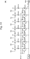
13 ein Schaltbild einer beispielhaften Schaltungsrealisierung des Off-Chip-Treibers aus 12 und 13 a circuit diagram of an exemplary circuit realization of the off-chip driver 12 and
14 ein Schaltbild einer beispielhaften Schaltungsrealisierung der Abschlussschaltung aus 12. 14 a circuit diagram of an exemplary circuit realization of the termination circuit 12 ,
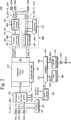
1 zeigt ein Blockschaltbild eines Ausführungsbeispiels einer erfindungsgemäßen integrierten Halbleiterspeicherschaltung 100. Wie aus 1 ersichtlich ist, ist der integrierte Halbleiterschaltungsbaustein 100 so ausgeführt, dass er mit anderen integrierten Schaltungsbausteinen kommuniziert, wobei er einen Empfänger 110 und einen Treiber 120 umfasst. Der Empfänger 110 ist über eine Signalübertragungsleitung TL0 mit einem Anschluss 131 verbunden, um externe Signale, wie Steuersignale oder Adressensignale, über den Anschluss 131 zu empfangen. Die Treiberschaltung 120 ist über eine Signalübertragungsleitung TL1 mit einem Anschluss 132 verbunden. Die Treiberschaltung 120 betreibt die Signalübertragungsleitung TL1 in Reaktion auf interne Signale, wie Datensignale. Der Empfänger 110 und der Treiber 120 sind beide mit einer internen Schaltung 140 verbunden. 1 shows a block diagram of an embodiment of an integrated semiconductor memory circuit according to the invention 100 , How out 1 is apparent, is the semiconductor integrated circuit device 100 designed to communicate with other integrated circuit devices, where it is a receiver 110 and a driver 120 includes. The recipient 110 is via a signal transmission line TL0 with a connection 131 connected to external signals, such as control signals or address signals, via the port 131 to recieve. The driver circuit 120 is via a signal transmission line TL1 with a connection 132 connected. The driver circuit 120 operates the signal transmission line TL1 in response to internal signals such as data signals. The recipient 110 and the driver 120 are both with an internal circuit 140 connected.
An die Signalübertragungsleitung TL0 ist eine Abschlussschaltung 150 gekoppelt. Der Anschluss 131 kann über eine externe Übertragungsleitung mit anderen integrierten Schaltungen verbunden sein. Die Abschlussschaltung 150 wird zur Verfügung gestellt, um die Signalübertragungsleitung TL0 abzuschließen und so Signalreflektionen zu reduzieren, die von Impedanzfehlanpassungen zwischen der nicht dargestellten externen Übertragungsleitung und dem Empfänger 110 verursacht werden. Eine Impedanzsteuerschaltung 160 ist mit einem Anschluss 133 verbunden, an den ein externer Referenzwiderstand REXT angeschlossen ist, und erzeugt einen variablen Steuercode gemäß der Impedanz des externen Referenzwiderstands REXT. Die Abschlussschaltung 150 und die Treiberschaltung 120 können mit variablen Impedanzen in gleichzeitiger Reaktion auf den Steuercode betrieben werden, der von der Impedanzsteuerschaltung 160 zugeführt wird. In anderen Worten ausgedrückt, die Impedanzsteuerschaltung 160 stellt die Impedanz der Abschlussschaltung 150 in variablen Optionen sowie auch der Treiberschaltung 120 gemäß der Impedanz variabel ein, die vom Referenzwiderstand REXT bereitgestellt wird.To the signal transmission line TL0 is a termination circuit 150 coupled. The connection 131 can be connected to other integrated circuits via an external transmission line. The final circuit 150 is provided to terminate the signal transmission line TL0 to reduce signal reflections resulting from impedance mismatches between the unillustrated external transmission line and the receiver 110 caused. An impedance control circuit 160 is with a connection 133 to which an external reference resistor REXT is connected, and generates a variable control code according to the impedance of the external reference resistor REXT. The final circuit 150 and the driver circuit 120 may be operated with variable impedances in concurrent response to the control code provided by the impedance control circuit 160 is supplied. In other words, the impedance control circuit 160 Represents the impedance of the termination circuit 150 in variable options as well as the driver circuit 120 in accordance with the impedance provided by the reference resistor REXT.
Das variable Impedanzsteuerschema kann für Halbleiterspeicherbausteine mit hoher Bandbreite als typische integrierte Schaltungschips verwendet werden und ist auch an andere Arten von integrierten Halbleiterschaltungsbausteinen anpassbar, die mit hohen Frequenzen betrieben werden.The variable impedance control scheme can be used for high bandwidth semiconductor memory devices as typical integrated circuit chips and is also adaptable to other types of semiconductor integrated circuit devices operating at high frequencies.
2 zeigt einen Halbleiterspeicherbaustein 200, der die Steuerfunktion für variable Impedanzen praktisch umsetzt. Der Halbleiterspeicherbaustein 200 kann mit hoher Bandbreite oder Frequenz und empfindlich gegenüber Kanalgegebenheiten betrieben werden, wie ein Speicher mit doppelter Datenrate (DDR) oder ein Speicher für höhere Frequenzen. 2 shows a semiconductor memory device 200 which practically implements the variable impedance control function. The semiconductor memory module 200 can operate at high bandwidth or frequency and sensitive to channel conditions, such as a double data rate (DDR) memory or higher frequency memory.
Wie aus 2 ersichtlich ist, umfasst der Speicherbaustein 200 ein Speicherzellenfeld 210, in dem Speicherzellen in einer Matrix aus Zeilen oder Wortleitungen und Spalten oder Bitleitungen angeordnet sind. Im Speicherbaustein 200 wählt ein Zeilendecoder 220 die Zeilen in Reaktion auf Zeilenadressen aus, die von einem Adressen- und Befehlspuffer 230 zur Verfügung gestellt werden. Ein Spaltendecoder 240 wählt die Spalten in Reaktion auf Spaltenadressen aus, die vom Adressen- und Befehlspuffer 230 zur Verfügung gestellt werden. Eine Abtastverstärkerschaltung 250 hält Daten, die aus dem Speicherzellenfeld 210 gelesen oder in das Speicherzellenfeld 210 geschrieben werden, auf einem ausreichenden Spannungspegel.How out 2 can be seen, includes the memory module 200 a memory cell array 210 in which memory cells are arranged in a matrix of rows or word lines and columns or bit lines. In the memory module 200 selects a row decoder 220 the lines in response to line addresses that come from an address and command buffer 230 to provide. A column decoder 240 selects the columns in response to column addresses from the address and command buffers 230 to provide. A sense amplifier circuit 250 Holds data from the memory cell array 210 read or in the memory cell array 210 written at a sufficient voltage level.
Eine Treibersteuerschaltung 260 empfängt Daten von der Abtastverstärkerschaltung 250 und erzeugt Aufwärts- bzw. Pull-up- sowie Abwärts- bzw. Pull-down-Steuersignale PUi und PDi in Reaktion auf Impedanzsteuercodes UPC und DNC. Hierbei wird der Code UPC benutzt, um die Impedanz zu erhöhen, während der Code DNC benutzt wird, um die Impedanz zu verkleinern. Eine Off-Chip-Treiberschaltung 270 gibt Ausgabesignalübertragungsleitungen TL_OUT1 bis TL_OUT3 in Reaktion auf die Aufwärts- und Abwärtssteuersignale PUi und PDi frei, die von der Treibersteuerschaltung 260 angelegt werden. Die Ausgabesignalübertragungsleitungen TL_OUT1 bis TL_OUT3 sind jeweils mit ihren korrespondierenden Anschlüssen PAD4 bis PAD6 verbunden. Eine Impedanz des Off-Chip-Treibers 270 ist gemäß der selektiven Aktivierung der Aufwärts- und Abwärtssteuersignale PUi und PDi variabel, was später detaillierter beschrieben wird. Die Dateneingabeschaltung 280 ist über Eingabesignalübertragungsleitungen TL_IN10 bis TL_IN30 mit den Anschlüssen PAD4 bis PAD6 verbunden, um Daten von den Anschlüssen PAD4 bis PAD6 zur Abtastverstärkerschaltung 250 zu übertragen. Mit den Eingabesignalübertragungsleitungen TL_IN10 bis TL_IN30 ist eine Abschlussschaltung 290 gekoppelt. Die Abschlussschaltung 290 wird in Reaktion auf den Impedanzsteuercode UPC oder auf beide Impedanzsteuercodes UPC und DNC betrieben und schließt die Eingabesignalübertragungsleitungen TL_IN10 bis TL_IN30 ab, um Signalreflektionen zu reduzieren, welche von Impedanzfehlanpassungen zwischen einer nicht dargestellten externen Übertragungsleitung und der Dateneingabeschaltung verursacht werden, welche mit dem Empfänger 110 aus 1 korrespondiert.A driver control circuit 260 receives data from the sense amplifier circuit 250 and generates pull-up and pull-down control signals PUi and PDi in response to impedance control codes UPC and DNC. Here, the code UPC is used to increase the impedance, while the code DNC is used to reduce the impedance. An off-chip driver circuit 270 enables output signal transmission lines TL_OUT1 to TL_OUT3 in response to the up and down control signals PUi and PDi sent from the driver control circuit 260 be created. The output signal transmission lines TL_OUT1 to TL_OUT3 are respectively connected to their corresponding terminals PAD4 to PAD6. An impedance of the off-chip driver 270 is variable according to the selective activation of the up and down control signals PUi and PDi, which will be described later in more detail. The data input circuit 280 is connected to the terminals PAD4 to PAD6 via input signal transmission lines TL_IN10 to TL_IN30 to input data from the terminals PAD4 to PAD6 to the sense amplifier circuit 250 transferred to. With the input signal transmission lines TL_IN10 to TL_IN30 is a termination circuit 290 coupled. The final circuit 290 is operated in response to the impedance control code UPC or both impedance control codes UPC and DNC and terminates the input signal transmission lines TL_IN10 to TL_IN30 to reduce signal reflections caused by impedance mismatches between an unillustrated external transmission line and the data input circuit connected to the receiver 110 out 1 corresponds.
Bei dieser Ausführungsform sind die Treibersteuerschaltung 260 und die Off-Chip-Treiberschaltung 270 während einer Aktivierung eines für einen Lesevorgang relevanten Steuersignals REN, d. h. eines Lesefreigabesignals, leitend geschaltet, während die Dateneingabeschaltung 280 und die Abschlussschaltung 290 während einer Aktivierung eines für einen Schreibvorgang relevanten Steuersignals WEN, d. h. eines Schreibfreigabesignals, leitend geschaltet sind.In this embodiment, the driver control circuit 260 and the off-chip driver circuit 270 during activation of a read-relevant control signal REN, ie, a read enable signal, turned on while the data input circuit 280 and the termination circuit 290 during an activation of a relevant for a write control signal WEN, ie a write enable signal, are turned on.
Wie aus 2 ersichtlich ist, ist der Adressen- und Befehlspuffer 230 über Eingabesignalübertragungsleitungen TL_IN11 bis TL_IN31 mit Anschlüssen PAD1 bis PAD3 verbunden, um Adressen- und Befehlssignale in vorgegebenen Zeittakten von einer externen Schaltung zu empfangen, wie von einer Speichersteuerschaltung. Zeilenadressen unter den eingegebenen Adressen werden zum Zeilendecoder 220 und Spaltenadressen werden zum Spaltendecoder 240 übertragen. An die Eingabesignalübertragungsleitungen TL_IN11 bis TL_IN31 ist eine Abschlussschaltung 300 gekoppelt. Die Abschlussschaltung 300 wird in Reaktion auf den Impedanzsteuercode UPC oder auf beide Impedanzsteuercodes UPC und DNC betrieben und schließt die Eingabesignalübertragungsleitungen TL_IN11 bis TL_IN31 ab, um Signalreflektionen zu reduzieren, welche von Impedanzfehlanpassungen zwischen einer nicht dargestellten, externen Übertragungsleitung und dem Adressen- und Befehlspuffer 230 verursacht werden, welcher mit dem Empfänger 110 aus 1 korrespondiert.How out 2 is apparent, is the address and command buffer 230 via input signal transmission lines TL_IN11 to TL_IN31 to terminals PAD1 to PAD3 for receiving address and command signals at predetermined timing from an external circuit, such as a memory control circuit. Row addresses below the entered addresses become the row decoder 220 and column addresses become the column decoder 240 transfer. To the input signal transmission lines TL_IN11 to TL_IN31 is a termination circuit 300 coupled. The final circuit 300 is operated in response to the impedance control code UPC or both impedance control codes UPC and DNC and terminates the input signal transmission lines TL_IN11 to TL_IN31 to reduce signal reflections resulting from impedance mismatches between an unillustrated external transmission line and the address and command buffer 230 caused, which with the receiver 110 out 1 corresponds.
Wie weiter aus 2 ersichtlich ist, ist ein Anschluss PAD7 mit einem externen Referenzwiderstand REXT und einem Generator 310 für variable Impedanzcodes verbunden. Der Generator 310 für variable Impedanzcodes erzeugt die Impedanzcodes UPCV und DNCV variabel in Abhängigkeit von einer Impedanz des externen Referenzwiderstandes REXT. Ein Generator 320 für feste Impedanzcodes erzeugt hingegen feste Impedanzsteuercodes UPCF und DNCF unabhängig von der Impedanz des externen Referenzwiderstandes REXT. Die Erzeugung der variablen und festen Impedanzsteuercodes wird später detaillierter beschrieben. Ein Programmregister 330 ist so gebildet, dass es durch Befehlssignale programmierbar ist, die von extern zur Verfügung gestellt werden, und erzeugt ein Codeauswahlsignal SEL und Offsetauswahlsignale OFFSET1 und OFFSET2. Das Programmregister 330 kann beispielsweise durch eine Schaltungsmethode eines Modusregistersatzes implementiert sein, die allgemein bekannt ist. Eine Auswahlschaltung 340 bestimmt in Reaktion auf das Codeauswahlsignal SEL die Steuercodes UPC und DNC aus den variablen Impedanzsteuercodes UPCV und DNCV, die vom Generator 310 zur Verfügung gestellt werden, und aus den festen Impedanzsteuercodes UPCF und DNCF, die vom Codegenerator 320 zur Verfügung gestellt werden. Die ausgewählten Steuercodes UPC und DNC werden an die Treibersteuerschaltung 260 und die Abschlussschaltungen 290 und 300 angelegt.How farther 2 is apparent, is a port PAD7 with an external reference resistor REXT and a generator 310 connected for variable impedance codes. The generator 310 for variable impedance codes, the impedance codes UPCV and DNCV are variably generated in response to an impedance of the external reference resistor REXT. A generator 320 for fixed impedance codes, on the other hand, fixed impedance control codes UPCF and DNCF are generated independently of the impedance of the external reference resistor REXT. The generation of the variable and fixed impedance control codes will be described later in more detail. A program register 330 is formed to be programmable by command signals provided externally, and generates a code selection signal SEL and offset selection signals OFFSET1 and OFFSET2. The program register 330 For example, it may be implemented by a circuit method of a mode register set which is well known. A selection circuit 340 In response to the code selection signal SEL, determines the control codes UPC and DNC from the variable impedance control codes UPCV and DNCV received from the generator 310 and from the fixed impedance control codes UPCF and DNCF generated by the code generator 320 to provide. The selected control codes UPC and DNC are sent to the driver control circuit 260 and the termination circuits 290 and 300 created.
Aus den obigen Ausführungen ergibt sich, dass die Impedanzen der Abschlussschaltungen 290 und 300 durch die Steuercodes UPC und DNC variabel sind, ebenso die Impedanz des Off-Chip-Treibers 270. Das bedeutet, dass ein einziger externer Referenzwiderstand, wie REXT, und ein Impedanzcodegenerator, wie der Generator 310, ausreichend sind, um die Impedanz des Off-Chip-Treibers 270 und der Abschlussschaltungen 290 und 300 in einem gleichzeitigen Modus zu steuern.From the above, it follows that the impedances of the termination circuits 290 and 300 are variable by the control codes UPC and DNC, as well as the impedance of the off-chip driver 270 , This means that a single external reference resistor, like REXT, and an impedance code generator, like the generator 310 , are sufficient to match the impedance of the off-chip driver 270 and the terminators 290 and 300 in a simultaneous mode to control.
3 zeigt ein Blockschaltbild einer bevorzugten funktionalen Struktur des Generators 310 für variable Impedanzcodes aus 2. Wie aus 3 ersichtlich ist, umfasst der Generator 310 für variable Impedanzcodes in diesem Beispiel einen ersten und einen zweiten Komparator 311 und 312, einen ersten und einen zweiten Zähler 313 und 314 und Schaltungen mit variabler Impedanz 315, 316 und 317. 3 shows a block diagram of a preferred functional structure of the generator 310 for variable impedance codes 2 , How out 3 can be seen, includes the generator 310 for variable impedance codes in this example a first and a second comparator 311 and 312 , a first and a second counter 313 and 314 and variable impedance circuits 315 . 316 and 317 ,
Der erste Komparator 311 detektiert, ob eine Spannung am Anschluss PAD7 höher als eine vorbestimmte Referenzspannung VREF ist oder nicht, die beispielsweise gleich VDDQ/2 sein kann. Der erste Zähler 313 erzeugt den variablen Impedanzsteuercode UPCV in Reaktion auf eine Ausgabe des ersten Komparators 311. Die Impedanzen der Schaltungen 315 und 316 sind vom Wert des variablen Impedanzsteuercodes UPCV abhängig. Diese Vorgänge werden so lange wiederholt, bis die Spannung am Anschluss PAD7 die Referenzspannung VREF erreicht. Währenddessen detektiert der zweite Komparator 312, ob eine Spannung an einem internen Knoten ND10 höher als eine Spannung am Anschluss PAD7 ist oder nicht. Der zweite Zähler 314 erzeugt den variablen Impedanzsteuercode DNCV in Reaktion auf eine Ausgabe des zweiten Komparators 312. Die Impedanz der dritten Schaltung 317 ist vom Wert des variablen Impedanzsteuercodes DNCV abhängig. Diese Vorgänge werden so lange wiederholt, bis die Spannung am internen Knoten ND10 die Spannung am Anschluss PAD7 erreicht.The first comparator 311 detects whether or not a voltage at the terminal PAD7 is higher than a predetermined reference voltage VREF, which may be, for example, equal to VDDQ / 2. The first counter 313 generates the variable impedance control code UPCV in response to an output of the first comparator 311 , The impedances of the circuits 315 and 316 are dependent on the value of the variable impedance control code UPCV. These operations are repeated until the voltage at terminal PAD7 reaches the reference voltage VREF. Meanwhile, the second comparator detects 312 Whether or not a voltage at an internal node ND10 is higher than a voltage at the terminal PAD7. The second counter 314 generates the variable impedance control code DNCV in response to an output of the second comparator 312 , The impedance of the third circuit 317 is of value of the variable impedance control code DNCV. These operations are repeated until the voltage at internal node ND10 reaches the voltage at terminal PAD7.
Wird beispielsweise angenommen, dass der externe Referenzwiderstand REXT einen Wert von 24 Ω aufweist, dann werden die Schaltungen 315 bis 317 mit variabler Impedanz durch den Betrieb der Komparatoren und Zähler 311 bis 314 so gesteuert, dass ihre Impedanzen jeweils einen Wert von 24 Ω haben.Assuming, for example, that the external reference resistor REXT has a value of 24 Ω, then the circuits become 315 to 317 with variable impedance through the operation of the comparators and counters 311 to 314 controlled so that their impedances each have a value of 24 Ω.
Bei diesem Ausführungsbeispiel sind der erste und zweite Zähler 313 und 314 als Aufwärts-/Abwärtszähler mit sieben Bit aufgebaut, so dass die variablen Impedanzsteuercodes UPCV und DNCV jeweils aus sieben Bits aufgebaut sind. Diese Codeinformationen können jedoch durch implementierte Kapazitäten im Gerät auch nach Bedarf verändert werden.In this embodiment, the first and second counters 313 and 314 is constructed as an up / down counter with seven bits, so that the variable impedance control codes UPCV and DNCV are each made up of seven bits. However, this code information can also be changed as needed by implemented capacities in the device.
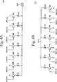
Die 4A und 4B zeigen jeweils ein Schaltbild von beispielhaften Realisierungen des Generators für variable Impedanzcodes aus 3. Die Schaltung 315 für variable Impedanz umfasst im Beispiel von 4A Paare von PMOS-Transistoren 64WP, 32WP, 16WP, ..., 2WP und 1WP und Widerständen 1R, 2R, 4R, ..., 64R, die mit je einem von einer Mehrzahl von verschiedenen Impedanzsteuercodes UPCV<6> bis UPCV<0> korrespondieren. In jedem Paar sind der PMOS-Transistor und der Widerstand in Reihe zwischen einer Versorgungsspannung und dem Anschluss PAD7 eingeschleift. Die PMOS-Transistoren 64WP bis 1WP der Schaltung 315 mit variabler Impedanz sind binär gewichtete Transistoren und die Widerstände 1R bis 64R der Schaltung 315 mit Variabler Impedanz sind binär gewichtete Widerstände. Die binär gewichteten Transistoren 64WP bis 1WP werden selektiv leitend geschaltet, gemäß einer passenden Aktivierung der variablen Impedanzsteuercodes UPCV<6> bis UPCV<0>, so dass die Schaltung 315 mit variabler Impedanz derart eingestellt wird, dass die Impedanz gleich derjenigen des externen Referenzwiderstandes REXT ist. Die zweite Schaltung 316 mit variabler Impedanz ist gleich wie die in 4A dargestellte Schaltung aufgebaut.The 4A and 4B each show a circuit diagram of exemplary realizations of the variable impedance generator 3 , The circuit 315 for variable impedance includes in the example of 4A Pairs of PMOS transistors 64WP, 32WP, 16WP, ..., 2WP and 1WP and resistors 1R, 2R, 4R, ..., 64R, each having one of a plurality of different impedance control codes UPCV <6> to UPCV <0 > correspond. In each pair, the PMOS transistor and the resistor are connected in series between a supply voltage and the terminal PAD7. The PMOS transistors 64WP to 1WP of the circuit 315 with variable impedance are binary weighted transistors and the resistors 1R to 64R of the circuit 315 with variable impedance are binary weighted resistors. The binary weighted transistors 64WP to 1WP are selectively turned on, in accordance with an appropriate activation of the variable impedance control codes UPCV <6> to UPCV <0>, so that the circuit 315 is set with variable impedance so that the impedance is equal to that of the external reference resistor REXT. The second circuit 316 with variable impedance is the same as the in 4A illustrated circuit constructed.
Die Schaltung 317 für variable Impedanz aus 4B umfasst Paare von NMOS-Transistoren (64WN, 32WN, 16WN, ..., 2WN und 1WN) und Widerständen (1R, 2R, 4R, ..., 64R), die mit je einem von einer Mehrzahl von verschiedenen Impedanzsteuercodes DNCV<6> bis DNCV<0> korrespondieren. In jedem Paar sind der NMOS-Transistor und der Widerstand in Reihe zwischen dem internen Knoten ND10 und einer Massespannung oder Substratspannung eingeschleift. Die NMOS-Transistoren 64WN bis 1WN der Schaltung 317 mit variabler Impedanz sind binär gewichtete Transistoren und die Widerstände 1R bis 64R der Schaltung 317 mit variabler Impedanz sind binär gewichtete Widerstände. Die binär gewichteten Transistoren 64WN bis 1WN werden selektiv leitend geschaltet, gemäß einer passenden Aktivierung der variablen Impedanzsteuercodes DNCV<6> bis DNCV<0>, so dass die Schaltung 317 mit variabler Impedanz derart eingestellt wird, dass die Impedanz gleich derjenigen des externen Referenzwiderstandes REXT ist.The circuit 317 for variable impedance 4B comprises pairs of NMOS transistors (64WN, 32WN, 16WN, ..., 2WN and 1WN) and resistors (1R, 2R, 4R, ..., 64R) each having one of a plurality of different impedance control codes DNCV <6 > to DNCV <0> correspond. In each pair, the NMOS transistor and the resistor are connected in series between the internal node ND10 and a ground voltage or substrate voltage. The NMOS transistors 64WN to 1WN of the circuit 317 with variable impedance are binary weighted transistors and the resistors 1R to 64R of the circuit 317 with variable impedance are binary weighted resistors. The binary weighted transistors 64WN to 1WN are selectively turned on, in accordance with an appropriate activation of the variable impedance control codes DNCV <6> to DNCV <0>, so that the circuit 317 is set with variable impedance so that the impedance is equal to that of the external reference resistor REXT.
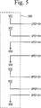
5 zeigt ein Schaltbild einer beispielhaften Realisierung des Generators 320 für feste Impedanzcodes aus 2. Wie aus 5 ersichtlich ist, ist der Generator 320 so ausgeführt, dass er feste Impedanzsteuercodes UPCF<0> bis UPCF<6> mit der Versorgungsspannung oder der Massespannung gemäß vorbestimmter Werte verbindet. In nicht dargestellter Weise kann der Generator 320 für feste Impedanzcodes auch so ausgeführt sein, dass die festen Impedanzsteuercodes durch externe Daten programmierbar sind. Daher können die festen Impedanzsteuercodes UPCF durch die Verbindungsoption aus 5 oder durch die Programmieroption erzeugt werden. Zusätzlich können die festen Impedanzsteuercodes UPCF als deren entsprechende Impedanzsteuercodes DNCF genutzt werden. 5 shows a circuit diagram of an exemplary implementation of the generator 320 for fixed impedance codes 2 , How out 5 it can be seen is the generator 320 is configured to connect fixed impedance control codes UPCF <0> to UPCF <6> to the supply voltage or the ground voltage according to predetermined values. In a manner not shown, the generator 320 for fixed impedance codes also be designed so that the fixed impedance control codes are programmable by external data. Therefore, the fixed impedance control codes UPCF can be enabled by the connection option 5 or generated by the programming option. In addition, the fixed impedance control codes UPCF may be used as their corresponding impedance control codes DNCF.
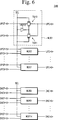
6 zeigt ein Ausführungsbeispiel der Auswahlschaltung 340 aus 2. Wie aus 6 ersichtlich ist, umfasst der Selektor 340 in diesem Fall eine Mehrzahl von 2:1-Multiplexern, z. B. vierzehn Multiplexer MUX1 bis MUX14. Jeder der Multiplexer ist aus einem Inverter INV10 und Übertragungsgattern TG10 und TG11 gebildet, wie im Block des MUX1 dargestellt ist. Die anderen Multiplexer MUX2 bis MUX14 sind gleich aufgebaut wie der MUX1. Jeder Multiplexer empfängt ein Paar der variablen und festen Impedanzsteuercodes, das ihm zugeordnet ist, und gibt den daraus ausgewählten Impedanzsteuercode aus. Eine erste Gruppe MUX1 bis MUX7 der Multiplexer wird benutzt, um die Impedanzsteuercodes UPC<6:0> in Reaktion auf die variablen und festen Impedanzsteuercodes UPCV<6:0> und UPCF<6:0> festzulegen. Eine zweite Gruppe MUX8 bis MUX14 der Multiplexer wird benutzt, um die Impedanzsteuercodes DNC<6:0> in Reaktion auf die variablen und festen Impedanzsteuercodes DNCV<6:0> und DNCF<6:0> festzulegen. So empfängt z. B. in der ersten Multiplexergruppe der Multiplexer MUX1 den variablen Impedanzsteuercode UPCV<6>, der vom Generator 310 für variable Impedanzsteuercodes zur Verfügung gestellt wird, und den festen Impedanzsteuercode UPCF<6>, der vom Generator 320 für feste Impedanzsteuercodes zur Verfügung gestellt wird, und gibt dann den Impedanzsteuercode UPC<6> durch Auswahl eines der Codes UPCV<6> und UPCF<6> aus. Auf die gleiche Weise empfängt der Multiplexer MUX8 in der zweiten Multiplexergruppe den variablen Impedanzsteuercode DNCV<6>, der vom Generator 310 für variable Impedanzsteuercodes zur Verfügung gestellt wird, und den festen Impedanzsteuercode DNCF<6>, der vom Generator 320 für feste Impedanzsteuercodes zur Verfügung gestellt wird, und gibt dann den Impedanzsteuercode DNC<6> durch Auswahl eines der Code DNCV<6> und DNCF<6> aus. 6 shows an embodiment of the selection circuit 340 out 2 , How out 6 is apparent, the selector includes 340 in this case a plurality of 2: 1 multiplexers, e.g. B. fourteen multiplexers MUX1 to MUX14. Each of the multiplexers is formed of an inverter INV10 and transmission gates TG10 and TG11, as shown in the block of MUX1. The other multiplexers MUX2 to MUX14 have the same structure as the MUX1. Each multiplexer receives a pair of the variable and fixed impedance control codes associated therewith and outputs the impedance control code selected therefrom. A first group MUX1 to MUX7 of the multiplexers is used to set the impedance control codes UPC <6: 0> in response to the variable and fixed impedance control codes UPCV <6: 0> and UPCF <6: 0>. A second group MUX8 to MUX14 of the multiplexers is used to set the impedance control codes DNC <6: 0> in response to the variable and fixed impedance control codes DNCV <6: 0> and DNCF <6: 0>. So z. B. in the first multiplexer group of the multiplexer MUX1 the variable impedance control code UPCV <6> from the generator 310 for variable Impedanzsteuercode is provided, and the fixed impedance control code UPCF <6>, the generator 320 for fixed impedance control codes, and then outputs the impedance control code UPC <6> by selecting one of the codes UPCV <6> and UPCF <6>. In the same way, the multiplexer MUX8 in the second multiplexer group receives the variable impedance control code DNCV <6> generated by the generator 310 for variable impedance control codes, and the fixed impedance control code DNCF <6> supplied by the generator 320 for fixed impedance control codes, and then outputs the impedance control code DNC <6> by selecting one of the codes DNCV <6> and DNCF <6>.
Ist das Codeauswahlsignal SEL auf einem niedrigen Pegel, dann gibt die Auswahlschaltung 340 jeweils die variablen Impedanzsteuercodes UPCV<6:0> bzw. DNCV<6:0> als Ausgabecodes UPC<6:0> bzw. DN<6:0> frei. Ist das Codeauswahlsignal SEL auf einem hohen Pegel, dann gibt die Auswahlschaltung 340 jeweils die festen Impedanzsteuercodes UPCF<6:0> bzw. DNCF<6:0> als Ausgabecodes UPC<6:0> bzw. DN<6:0> frei.If the code selection signal SEL is at a low level, then the selection circuit outputs 340 in each case the variable impedance control codes UPCV <6: 0> or DNCV <6: 0> as output codes UPC <6: 0> or DN <6: 0> free. If the code selection signal SEL is at a high level, then the selection circuit outputs 340 in each case the fixed impedance control codes UPCF <6: 0> or DNCF <6: 0> as output codes UPC <6: 0> and DN <6: 0>, respectively.
7 zeigt ein Schaltbild einer beispielhaften Realisierung der Treibersteuerschaltung 260 aus 2. Wie aus 7 ersichtlich ist, empfängt die Treibersteuerschaltung 260 die Impedanzsteuercodes UPC<6:0> und DNC<6:0> vom Selektor 340 und ein Datenbit DATA<0> der Daten DATA_OUT von der Abtastverstärkerschaltung 250 und erzeugt Aufwärts- und Abwärtssteuersignale PU<6:0> und PD<6:0>. Die Treibersteuerschaltung 260 ist aus sieben NAND-Gattern G10 bis G16, sieben NOR-Gattern G17 bis G23 und sieben Invertern INV11 bis INV17 aufgebaut. Jedes der NAND-Gatter G10 bis G16 empfängt einen der Impedanzsteuercodes UPC<6:0> und gibt eines der Aufwärtssteuersignale PU<6:0> aus, gesteuert vom Datenbit DATA<0>. Jedes der NOR-Gatter G17 bis G23 empfängt einen der Impedanzsteuercodes DNC<6:0> über den jeweiligen Inverter INV11 bis INV17 und gibt eines der Abwärtssteuersignale PD<6:0> aus, gesteuert vom Datenbit DATA<0>. 7 shows a circuit diagram of an exemplary implementation of the driver control circuit 260 out 2 , How out 7 can be seen receives the driver control circuit 260 the impedance control codes UPC <6: 0> and DNC <6: 0> from the selector 340 and a data bit DATA <0> of the data DATA_OUT from the sense amplifier circuit 250 and generates up and down control signals PU <6: 0> and PD <6: 0>. The driver control circuit 260 is composed of seven NAND gates G10 to G16, seven NOR gates G17 to G23 and seven inverters INV11 to INV17. Each of the NAND gates G10 to G16 receives one of the impedance control codes UPC <6: 0> and outputs one of the up-control signals PU <6: 0> controlled by the data bit DATA <0>. Each of the NOR gates G17 to G23 receives one of the impedance control codes DNC <6: 0> via the respective inverters INV11 to INV17 and outputs one of the down control signals PD <6: 0> controlled by the data bit DATA <0>.
Hat das Datenbit DATA<0>, das von der Abtastverstärkerschaltung 250 zur Verfügung gestellt wird, den Wert „1” (Binärcode), dann sind die Aufwärtssteuersignale PU<6:0> von den variablen Impedanzsteuercodes UPC<6:0> abhängig. Hat beispielsweise das Codesignal UPC<6:0> den Wert „1010101”, dann sind PU<6>, PU<4>, PU<2> und PU<0> auf einem niedrigen Pegel, während PU<5>, PU<3> und PU<1> auf einen hohen Pegel gesetzt sind. Da das Datenbit DATA<0> den Wert „1” hat, werden alle Ausgaben der NOR-Gatter G17 bis G23, d. h. die Signale PD<6:0>, unabhängig vom Zustand ihrer Eingabesignale DNC<6:0> auf einem niedrigen Pegel gehalten.Has the data bit DATA <0>, that of the sense amplifier circuit 250 is provided with the value "1" (binary code), then the up-control signals PU <6: 0> are dependent on the variable impedance control codes UPC <6: 0>. If, for example, the code signal UPC <6: 0> has the value "1010101", then PU <6>, PU <4>, PU <2> and PU <0> are at a low level, while PU <5>, PU <3> and PU <1> are set to a high level. Since the data bit DATA <0> has the value "1", all outputs of the NOR gates G17 to G23, that is, the signals PD <6: 0> become low regardless of the state of their input signals DNC <6: 0> held.
Wenn andererseits das Datenbit DATA<0>, das von der Abtastverstärkerschaltung 250 zur Verfügung gestellt wird, den Wert „0” hat, dann sind die Abwärtssteuersignale PD<6:0> von den variablen Impedanzsteuercodes DNC<6:0> abhängig. Hat beispielsweise das Codesignal DNC<6:0> den Wert „1010101”, dann sind PD<6>, PD<4>, PD<2> und PD<0> auf einem niedrigen Pegel, während PD<5>, PD<3> und PD<1> auf einen hohen Pegel gesetzt sind. Da das Datenbit DATA<0> den Wert „0” hat, werden alle Ausgaben der NAND-Gatter G10 bis G16, d. h. die Signale PU<6:0>, unabhängig vom Zustand ihrer Eingabesignale UPC<6:0> auf einem niedrigen Pegel gehalten.On the other hand, if the data bit DATA <0>, that from the sense amplifier circuit 250 is provided with the value "0", then the down control signals PD <6: 0> are dependent on the variable impedance control codes DNC <6: 0>. For example, if the code signal DNC <6: 0> has the value "1010101", then PD <6>, PD <4>, PD <2> and PD <0> are at a low level, while PD <5>, PD <3> and PD <1> are set to a high level. Since the data bit DATA <0> has the value "0", all outputs of the NAND gates G10 to G16, that is, the signals PU <6: 0> become low regardless of the state of their input signals UPC <6: 0> held.
Entsprechend werden, wie oben erwähnt, die Aufwärtssteuersignale PU<6:0> selektiv entsprechend den variablen Impedanzsteuercodes UPC<6:0> freigegeben, wenn das Datenbit DATA<0>, das von der Abtastverstärkerschaltung 250 zur Verfügung gestellt wird, einen Wert „1” hat, während die Abwärtssteuersignale PD<6:0> selektiv entsprechend den variablen Impedanzsteuercodes DNC<6:0> freigegeben werden, wenn das Datenbit DATA<0> den Wert „1” hat. Die Aufwärts- und Abwärtssteuersignale UPC<6:0> und DNC<6:0> sind zueinander exklusiv.Accordingly, as mentioned above, the up-control signals PU <6: 0> are selectively enabled according to the variable impedance control codes UPC <6: 0> when the data bit DATA <0> supplied from the sense amplifier circuit 250 is provided has a value "1" while the down control signals PD <6: 0> are selectively enabled according to the variable impedance control codes DNC <6: 0> when the data bit DATA <0> is "1". The up and down control signals UPC <6: 0> and DNC <6: 0> are exclusive to each other.
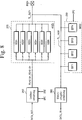
8 zeigt ein Blockschaltbild des Off-Chip-Treibers 270 und der Abschlussschaltung 290 aus 2 in einer vorteilhaften schaltungstechnischen Realisierung. Obwohl 8 nur Strukturen zeigt, die mit einem der Anschlüsse verknüpft sind, hier dem Anschluss PAD4, sind die anderen Anschlüsse IPAD5 bis PAD6 dazu entsprechend mit dem gleichen Schaltungsaufbau gemäß 8 angeordnet. 8th shows a block diagram of the off-chip driver 270 and the termination circuit 290 out 2 in an advantageous circuit implementation. Even though 8th only shows structures that are associated with one of the ports, here the port PAD4, the other ports IPAD5 to PAD6 are accordingly according to the same circuit configuration according to 8th arranged.
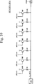
Wie aus 8 ersichtlich ist, umfasst der Off-Chip-Treiber 270 mehrere, z. B. sechs, Off-Chip-Treiberblöcke OCD1 bis OCD6. Die Off-Chip-Treiberblöcke OCD1 bis OCD6 aktivieren den zugehörigen Anschluss PAD4 bzw. die zugehörige Ausgabesignalübertragungsleitung TLOUT_1 in Reaktion auf die Aufwärts- und Abwärtssteuersignale PU<6:0> und PD<6:0>, die von der Treibersteuerschaltung 260 erzeugt werden. Jeder der Treiberblöcke ist z. B. aus binär gewichteten Transistoren und binär gewichteten Widerständen gebildet, wie aus einer möglichen schaltungstechnischen Realisierung gemäß 9 ersichtlich ist, die im übrigen selbsterklärend ist.How out 8th can be seen, includes the off-chip driver 270 several, z. B. six, off-chip driver blocks OCD1 to OCD6. The off-chip driver blocks OCD1 to OCD6 activate the associated port PAD4 and the associated output signal transmission line TLOUT_1 in response to the up and down control signals PU <6: 0> and PD <6: 0> generated by the driver control circuit 260 be generated. Each of the driver blocks is z. B. from binary weighted transistors and binary weighted resistors formed, as from a possible circuit implementation according to 9 which is otherwise self-explanatory.
Es wurde oben ausgeführt, dass im Generator 310 für variable Impedanzcodes die Schaltung 315 für variable Impedanz eine zur Impedanz des externen Referenzwiderstandes REXT identische Impedanz hat, wenn die Spannung am Anschluss PAD7 gleich der Referenzspannung VREF ist. Ebenfalls haben die Off-Chip-Treiberblöcke OCD1 bis OCD6, indem die Aufwärts- und Abwärtssteuersignale PU<6:0> und PD<6:0> selektiv gemäß den variablen Impedanzsteuercodes aktiviert werden, eine Impedanz, die zur Impedanz des externen Referenzwiderstands REXT identisch ist. Hat der externe Referenzwiderstand REXT beispielsweise einen Wert von 240 Ω, dann haben die Off-Chip-Treiberblöcke OCD1 bis OCD6 eine Impedanz von 240 Ω gemäß den Impedanzsteuercodes. Da die Off-Chip-Treiberblöcke OCD1 bis OCD6 zu jedem Anschluss parallel geschaltet sind, wird jeder Anschluss bzw. jede Ausgabesignalübertragungsleitung durch den Off-Chip-Treiber 270 mit einer Impedanz von 40 Ω getrieben.It was stated above that in the generator 310 for variable impedance codes the circuit 315 for variable impedance has an impedance identical to the impedance of the external reference resistor REXT when the voltage at the terminal PAD7 is equal to the reference voltage VREF. Also, by activating the up and down control signals PU <6: 0> and PD <6: 0> selectively in accordance with the variable impedance control codes, the off-chip driver blocks OCD1 to OCD6 have an impedance identical to the impedance of the external reference resistor REXT is. For example, if the external reference resistance REXT has a value of 240 Ω, the off-chip driver blocks OCD1 to OCD6 have an impedance of 240 Ω according to the impedance control codes. Because the off-chip driver blocks OCD1 to OCD6 are connected in parallel to each terminal, each terminal or each output signal transmission line is driven by the off-chip driver 270 driven with an impedance of 40 Ω.
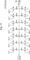
In 8 umfasst die Abschlussschaltung 290 vier Abschlussblöcke ODT1 bis ODT4, die parallel mit dem Anschluss PAD4 bzw. der Eingabesignalübertragungsleitung TL_IN10 verbunden sind. Jeder Abschlussblock schließt die Eingabesignalübertragungsleitung TL_IN10 in Reaktion auf den zugeordneten Impedanzsteuercode UPC ab und ist z. B. aus binär gewichteten Transistoren und binär gewichteten Widerständen aufgebaut, wie 10 für eine mögliche schaltungstechnische Realisierung zeigt, wobei der Schaltungsaufbau von 10 im übrigen selbsterklärend ist. Wie oben ausgeführt ist, hat im Generator 310 für variable Impedanzcodes die Schaltung 315 für variable Impedanz eine Impedanz, die mit der Impedanz des externen Referenzwiderstands REXT identisch ist, wenn die Spannung am Anschluss PAD7 gleich der Referenzspannung VREF ist. Ebenso haben die Abschlussblöcke ODT1 bis ODT6 eine Impedanz, die mit der Impedanz des externen Referenzwiderstandes identisch sind, indem die Impedanzsteuercodes UPC<6:0> identisch zu den variablen Impedanzsteuercodes sind. Hat der externe Referenzwiderstand REXT beispielsweise einen Wert von 240 Ω, dann haben die Off-Chip-Treiberblöcke OCD1 bis OCD6 gemäß den Impedanzsteuercodes eine Impedanz von 240 Ω. Da die vier Abschlussblöcke ODT1 bis ODT4 parallel mit dem betreffenden Anschluss verbunden sind, wird jeder Anschluss bzw. jede Ausgabesignalübertragungsleitung von der Abschlussschaltung 290 mit einer Impedanz von 60 Ω getrieben.In 8th includes the termination circuit 290 four termination blocks ODT1 to ODT4 connected in parallel with the terminal PAD4 and the input signal transmission line TL_IN10, respectively. Each termination block terminates the input signal transmission line TL_IN10 in response to the associated impedance control code UPC and is e.g. B. constructed of binary weighted transistors and binary weighted resistors, such as 10 for a possible circuit implementation shows, wherein the circuit structure of 10 otherwise self-explanatory. As stated above, in the generator 310 for variable impedance codes the circuit 315 for variable impedance, an impedance which is identical to the impedance of the external reference resistor REXT when the voltage at the terminal PAD7 is equal to the reference voltage VREF. Similarly, the termination blocks ODT1 to ODT6 have an impedance identical to the impedance of the external reference resistor in that the impedance control codes UPC <6: 0> are identical to the variable impedance control codes. For example, if the external reference resistor REXT has a value of 240 Ω, then the off-chip driver blocks OCD1 to OCD6 have an impedance of 240 Ω according to the impedance control codes. Since the four termination blocks ODT1 to ODT4 are connected in parallel with the respective terminal, each terminal or each output signal transmission line is terminated by the termination circuit 290 driven with an impedance of 60 Ω.
Während in 8 die Abschlussschaltung 290 so ausgeführt ist, dass sie von den Impedanzsteuercodes UPC gesteuert wird, die von der Auswahlschaltung 340 aus 2 erzeugt werden, kann sie auch so ausgeführt sein, dass sie mit allen Impedanzsteuercodes UPC<6:0> und DNC<6:0> betrieben wird, wofür eine schaltungstechnische Realisierung in der selbsterklärenden 11 dargestellt ist. Die andere Abschlussschaltung 300, die mit den Eingabesignalübertragungsleitungen TL_IN11 bis TL_IN31 assoziiert ist, kann mit der gleichen Struktur, wie sie in den 8, 10 und 11 dargestellt ist, ausgeführt sein, was nicht weiter dargestellt ist.While in 8th the termination circuit 290 is designed to be controlled by the impedance control codes UPC, that of the selection circuit 340 out 2 can be designed so that it is operated with all impedance control codes UPC <6: 0> and DNC <6: 0>, for which a circuit implementation in the self-explanatory 11 is shown. The other termination circuit 300 , which is associated with the input signal transmission lines TL_IN11 to TL_IN31, may have the same structure as described in FIGS 8th . 10 and 11 is shown, executed, which is not shown.
Nachfolgend wird die Funktionsweise zum Einstellen der Impedanz der Abschlussschaltung und des Off-Chip-Treibers in Verbindung mit den zugehörigen Figuren näher beschrieben.The operation for adjusting the impedance of the termination circuit and the off-chip driver in conjunction with the associated figures will be described in more detail below.
Das Programmregister 330 ist programmierbar festgelegt, um aus den festen Impedanzsteuercodes UPCF<6:0> und DNCF<6:0> und variablen Impedanzsteuercodes UPCV<6:0> und DNCV<6:0> auszuwählen. Im dargestellten Ausführungsbeispiel ist das Programmregister 330 so programmiert, dass es die variablen Impedanzsteuercodes UPCV<6:0> und DNCV<6:0> auswählt. Das Programmregister 310 erzeugt das Codeauswahlsignal SEL mit niedrigem Pegel, um die Auswahlschaltung 340 zu veranlassen, die Ausgabe des Generators 310 für variable Impedanzcodes auszuwählen. Der Generator 310 gibt die variablen Impedanzsteuercodes UPCV<6:0> und DNCV<6:0> orientiert an der Impedanz des externen Referenzwiderstands REXT aus, der mit dem Anschluss PAD7 verbunden ist. Die variablen Impedanzsteuercodes werden zu den Abschlussschaltungen 290 und 300 und zur Treibersteuerschaltung 260 übertragen. Die Auswahlschaltung 340 kann z. B. nur mit den Impedanzsteuercodes UPC<6:0> oder mit den beiden Arten von Impedanzsteuercodes UPC<6:0> und DNC<6:0> assoziiert sein.The program register 330 is programmably set to select from the fixed impedance control codes UPCF <6: 0> and DNCF <6: 0> and variable impedance control codes UPCV <6: 0> and DNCV <6: 0>. In the illustrated embodiment, the program register 330 programmed to select the variable impedance control codes UPCV <6: 0> and DNCV <6: 0>. The program register 310 generates the code selection signal SEL of low level to the selection circuit 340 to induce the output of the generator 310 for variable impedance codes. The generator 310 outputs the variable impedance control codes UPCV <6: 0> and DNCV <6: 0> based on the impedance of the external reference resistor REXT connected to the terminal PAD7. The variable impedance control codes become the termination circuits 290 and 300 and the driver control circuit 260 transfer. The selection circuit 340 can z. B. only with the impedance control codes UPC <6: 0> or with the two types of impedance control codes UPC <6: 0> and DNC <6: 0> be associated.
Die Abschlussschaltung 300 schließt die Eingabesignalübertragungsleitungen TL_IN11 bis TL_IN31 in Reaktion auf den Impedanzsteuercode UPC<6:0> ab. Die Abschlussschaltung 290 schließt die Eingabesignalübertragungsleitungen TL_IN10 bis TL_IN30 in Reaktion auf den Impedanzsteuercode UPC<6:0> während eines Schreibvorgangs ab. Die Abschlussschaltungen 290 und 300 haben die gleiche Impedanz, beispielsweise 60 Ω, wenn der externe Referenzwiderstand REXT, der mit dem Anschluss PAD7 verbunden ist, einen Wert von 240 Ω hat. Dies kommt daher, dass die vier Abschlussblöcke ODT1 bis ODT4 jeder Abschlussschaltung parallel mit deren korrespondierendem Anschluss bzw. Eingabesignalübertragungsleitung verbunden sind und durch den gleichen Impedanzsteuercode für die Impedanzübereinstimmung, z. B. 240 Ω, mit dem externen Referenzwiderstand gesteuert werden.The final circuit 300 terminates the input signal transmission lines TL_IN11 to TL_IN31 in response to the impedance control code UPC <6: 0>. The final circuit 290 terminates the input signal transmission lines TL_IN10 to TL_IN30 in response to the impedance control code UPC <6: 0> during a write operation. The termination circuits 290 and 300 have the same impedance, for example 60 Ω, when the external reference resistance REXT connected to the terminal PAD7 has a value of 240 Ω. This is because the four termination blocks ODT1 to ODT4 of each termination circuit are connected in parallel with their corresponding input signal transmission line and are given the same impedance control code for impedance matching, e.g. B. 240 Ω, are controlled with the external reference resistor.
Gleichzeitig wird der von der Auswahlschaltung 340 ausgewählte Impedanzsteuercode UPC<6:0> oder DNC<6:0> zur Treibersteuerschaltung 260 übertragen. Die Treibersteuerschaltung 260 erzeugt das Aufwärtssteuersignal PU<6:0> oder das Abwärtssteuersignal PD<6:0> gemäß den Daten DATA_OUT, d. h. DATA<0>, die von der Abtastverstärkerschaltung 250 zur Verfügung gestellt werden. Das Aufwärtssteuersignal PU<6:0> bzw. das Abwärtssteuersignal PD<6:0> ist identisch mit dem Impedanzsteuercode UPC<6:0> oder DNC<6:0>. Hat der externe Referenzwiderstand REXT, der mit dem Anschluss PAD7 verbunden ist, einen Wert von 240 Ω, dann hat der Off-Chip-Treiber 270 eine Impedanz von 40 Ω. Dies kommt daher, dass die sechs Off-Chip-Treiberblöcke OCD1 bis OCD6 jedes Off-Chip-Treibers parallel mit dessen korrespondierendem Anschluss bzw. Eingabesignalübertragungsleitung verbunden sind und durch die gleichen Aufwärts- und Abwärtssteuersignale für die Impedanzübereinstimmung, z. B. 240 Ω, mit dem externen Referenzwiderstand gesteuert werden.At the same time, that of the selection circuit 340 selected impedance control code UPC <6: 0> or DNC <6: 0> to the driver control circuit 260 transfer. The driver control circuit 260 generates the up-control signal PU <6: 0> or the down-control signal PD <6: 0> in accordance with the data DATA_OUT, that is, DATA <0> supplied from the sense amplifier circuit 250 to provide. The up control signal PU <6: 0> and the down control signal PD <6: 0> are identical to the impedance control code UPC <6: 0> or DNC <6: 0>. If the external reference resistor REXT connected to the terminal PAD7 has a value of 240 Ω, then the off-chip driver has 270 an impedance of 40 Ω. This is because the six off-chip driver blocks OCD1 to OCD6 of each off-chip driver are connected in parallel with its corresponding input signal transmission line and are driven by the same impedance matching up and down control signals, e.g. B. 240 Ω, are controlled with the external reference resistor.
Während eines Lesevorgangs werden die Abschlussschaltung 300 und der Off-Chip-Treiber 270 gleichzeitig von den Impedanzsteuercodes UPC<6:0> und DNC<6:0> gesteuert, die zur Angleichung der geforderten Impedanz ausgewählt werden. Analog werden während eines Schreibvorgangs die Abschlussschaltungen 290 und 300 von den Impedanzsteuercodes UPC<6:0> und DNC>6:0> stellen die Impedanz der Abschlussschaltungen 290 und 300 ein und steuern zudem die Impedanz der Off-Chip-Treiberschaltung 270. Deshalb ist es möglich, die Impedanz der Abschlussschaltungen 290 und 300 und des Off-Chip-Treibers 270 gleichzeitig mittels eines einzelnen externen Referenzwiderstandes, z. B. REXT, und eines Impedanzcodegenerators, z. B. 310 oder 320, einzustellen. During a read operation the termination circuit 300 and the off-chip driver 270 controlled simultaneously by the impedance control codes UPC <6: 0> and DNC <6: 0>, which are selected to equalize the required impedance. Similarly, during a write operation, the termination circuits become 290 and 300 of the impedance control codes UPC <6: 0> and DNC> 6: 0> represent the impedance of the termination circuits 290 and 300 and also control the impedance of the off-chip driver circuit 270 , Therefore, it is possible the impedance of the termination circuits 290 and 300 and the off-chip driver 270 simultaneously by means of a single external reference resistor, z. REXT, and an impedance code generator, e.g. B. 310 or 320 to adjust.
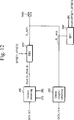
12 zeigt ein Blockschaltbild einer anderen Ausführungsform des Off-Chip-Treibers und der Abschlussschaltung aus 2. Im Gegensatz zur Schaltung aus 8 ist die Off-Chip-Treiberschaltung 270' mit einem einzelnen Off-Chip-Treiberblock OCD1 ausgeführt, dessen Impedanz gemäß den Offsetauswahlsignalen OFFSET0 und OFFSET1 genau einstellbar ist. Wie aus 13 ersichtlich ist, ist die Off-Chip-Treiberschaltung 270' aus einem Pull-up-Teil bzw. Aufwärtsteil 271 und einem Pull-down-Teil bzw. Abwärtsteil 272 aufgebaut. Der Aufwärtsteil 271 ist aus binär gewichteten Transistoren 64WP/N bis 1WP/N und binär gewichteten Widerständen 1R/N bis 64R/N aufgebaut. Um den Off-Chip-Treiber 270' mit einer Impedanz von 40 Ω zu implementieren, sind die binär gewichteten Transistoren 64WP/N bis 1WP/N und Widerstände 1R/N bis 64R/N als um den Faktor 1/N linear verkleinerte Transistoren und Widerstände aus den 9, 10 oder 11 ausgeführt. Die binär gewichteten Transistoren 64WP/N bis 1WP/N werden von den Aufwärtssteuersignalen PU<6:0> gesteuert, so dass der Anschluss PAD4 vom Off-Chip-Treiber 270' mit einer Impedanz von 40 Ω getrieben wird. 12 Figure 12 is a block diagram of another embodiment of the off-chip driver and the termination circuit 2 , Unlike the circuit 8th is the off-chip driver circuit 270 ' with a single off-chip driver block OCD1 whose impedance is precisely adjustable according to the offset select signals OFFSET0 and OFFSET1. How out 13 is apparent, is the off-chip driver circuit 270 ' from a pull-up part or upwards part 271 and a pull-down part 272 built up. The upside part 271 is constructed of binary weighted transistors 64WP / N through 1WP / N and binary weighted resistors 1R / N through 64R / N. To the off-chip driver 270 ' with an impedance of 40 Ω, the binary weighted transistors 64WP / N through 1WP / N and resistors 1R / N through 64R / N are linearly reduced by a factor of 1 / N, and resistors are made of the 9 . 10 or 11 executed. The binary weighted transistors 64WP / N through 1WP / N are controlled by the boost control signals PU <6: 0>, so that the port PAD4 from the off-chip driver 270 ' with an impedance of 40 Ω.
Der Aufwärtsteil 271 umfasst des Weiteren Offsetwiderstände OFR1 bis OFR7 und Offsettransistoren OFT1 bis OFT7. Die Offsettransistoren OFT1 bis OFT7 werden gleichzeitig vom Offsetauswahlsignal OFFSET1 gesteuert. Die Impedanz des Aufwärtsteils 271 kann gemäß einer Aktivierung des Offsetauswahlsignals OFFSET1 eingestellt werden. Die Offsettransistoren OFT1 bis OFT7 können in der gleichen Transistordimension oder in der binär gewichteten Form ausgeführt sein. Ebenso können die Offsetwiderstände OFR1 bis OFR7 mit der gleichen Widerstanddimensionierung oder in der binär gewichteten Form ausgeführt sein.The upside part 271 further comprises offset resistors OFR1 to OFR7 and offset transistors OFT1 to OFT7. The offset transistors OFT1 to OFT7 are simultaneously controlled by the offset selection signal OFFSET1. The impedance of the upward part 271 can be set in accordance with activation of the offset selection signal OFFSET1. The offset transistors OFT1 to OFT7 may be implemented in the same transistor dimension or in the binary weighted form. Likewise, the offset resistors OFR1 to OFR7 may be implemented with the same resistance dimensioning or in the binary weighted form.
Der Abwärtsteil 272 ist aus binär gewichteten Transistoren 64WN/N bis 1WN/N und binär gewichteten Widerständen 1R/N bis 64R/N aufgebaut. Um den Off-Chip-Treiber 270' mit einer Impedanz von 60 Ω zu implementieren, sind die binär gewichteten Transistoren 64WN/N bis 1WN/N und Widerstände IRIN bis 64R/N als um den Faktor 1/N linear verkleinerte Transistoren und Widerstände aus den 9, 10 oder 11 ausgeführt. Die binär gewichteten Transistoren 64WN/N bis 1WN/N werden von den Abwärtssteuersignalen PD<6:0> gesteuert, wodurch der Anschluss PAD4 von der Off-Chip-Treiberschaltung 270' mit einer Impedanz von 60 Ω getrieben wird.The downside part 272 is constructed of binary weighted transistors 64WN / N through 1WN / N and binary weighted resistors 1R / N through 64R / N. To the off-chip driver 270 ' With an impedance of 60 Ω, the binary weighted transistors 64WN / N to 1WN / N and resistors IRIN to 64R / N are linearly reduced by a factor of 1 / N, and resistors are made of the 9 . 10 or 11 executed. The binary weighted transistors 64WN / N through 1WN / N are controlled by the down control signals PD <6: 0>, whereby the terminal PAD4 from the off-chip driver circuit 270 ' is driven with an impedance of 60 Ω.
Der Abwärtsteil 272 umfasst des Weiteren Offsetwiderstände OFR8 bis OFR14 und Offsettransistoren OFT8 bis OFT14. Die Offsettransistoren OFT8 bis OFT14 werden gleichzeitig vom Offsetauswahlsignal OFFSET2 gesteuert. Die Impedanz des Abwärtsteils 272 kann gemäß einer Aktivierung des Offsetauswahlsignals OFFSET2 eingestellt werden. Die Offsettransistoren OFT8 bis OFT14 können mit der gleichen Transistordimension oder in der binär gewichteten Form ausgeführt sein. Ebenso können die Offsetwiderstände OFR8 bis OFR14 mit der gleichen Widerstanddimensionierung oder in der binär gewichteten Form ausgeführt sein.The downside part 272 further comprises offset resistors OFR8 to OFR14 and offset transistors OFT8 to OFT14. The offset transistors OFT8 to OFT14 are simultaneously controlled by the offset selection signal OFFSET2. The impedance of the downward part 272 can be set in accordance with activation of the offset selection signal OFFSET2. The offset transistors OFT8 to OFT14 may be implemented with the same transistor dimension or in the binary weighted form. Likewise, the offset resistors OFR8 to OFR14 may be implemented with the same resistance dimensioning or in the binary weighted form.
Wie aus 12 weiter ersichtlich ist, ist im Vergleich zur 8 eine andere Abschlussschaltung 290' mit einem einzigen Abschlussblock ODT1 vorgesehen. Die Impedanz der Abschlussschaltung 290' kann gemäß den Offsetauswahlsignalen OFFSET0 und OFFSET1 genau eingestellt werden. Wie aus 14 ersichtlich ist, ist die Abschlussschaltung 290' in der dort gezeigten Realisierung aus binär gewichteten Transistoren 64WN/N bis 1WN/N und binär gewichteten Widerständen 1R/N bis 64R/N aufgebaut. Um die Abschlussschaltung 290' mit einer Impedanz von 40 Ω zu implementieren, sind die binär gewichteten Transistoren 64WN/N bis 1WN/N und Widerstände 1R/N bis 64R/N als um den Faktor 1/N linear verkleinerte Transistoren und Widerstände aus den 9, 10 oder 11 ausgeführt. Die binär gewichteten Transistoren 64WN/N bis 1WN/N werden von den Aufwärtssteuersignalen PU<6:0> gesteuert, wobei die Eingabesignalübertragungsleitung TL_IN10 durch die Abschlussschaltung 290' mit einer Impedanz von 40 Ω abgeschlossen wird.How out 12 is apparent, is compared to 8th another termination circuit 290 ' provided with a single termination block ODT1. The impedance of the termination circuit 290 ' can be set accurately according to the offset selection signals OFFSET0 and OFFSET1. How out 14 is apparent, is the termination circuit 290 ' In the realization shown there, constructed from binary weighted transistors 64WN / N to 1WN / N and binary weighted resistors 1R / N to 64R / N. To the termination circuit 290 ' With an impedance of 40 Ω, the binary weighted transistors 64WN / N through 1WN / N and resistors 1R / N through 64R / N are transistors linearly reduced by a factor of 1 / N, and resistors of the 9 . 10 or 11 executed. The binary weighted transistors 64WN / N through 1WN / N are controlled by the boost control signals PU <6: 0>, the input signal transmission line TL_IN10 being driven by the termination circuit 290 ' is completed with an impedance of 40 Ω.
Die Abschlussschaltung 290' umfasst des Weiteren Offsetwiderstände OFR15 bis OFR21 und Offsettransistoren OFT15 bis OFT21. Die Offsettransistoren OFT15 bis OFT21 werden gleichzeitig vom Offsetauswahlsignal OFFSET1 gesteuert. Die Impedanz der Abschlussschaltung 290' kann gemäß einer Aktivierung des Offsetauswahlsignals OFFSET1 eingestellt werden. Die Offsettransistoren OFT15 bis OFT21 können mit der gleichen Transistordimension oder in der binär gewichteten Form ausgeführt sein. Ebenso können die Offsetwiderstände OFR15 bis OFR21 mit der gleichen Widerstanddimensionierung oder in der binär gewichteten Form ausgeführt sein.The final circuit 290 ' further comprises offset resistors OFR15 to OFR21 and offset transistors OFT15 to OFT21. The offset transistors OFT15 to OFT21 are simultaneously controlled by the offset selection signal OFFSET1. The impedance of the termination circuit 290 ' can be set in accordance with activation of the offset selection signal OFFSET1. The offset transistors OFT15 to OFT21 may be implemented with the same transistor dimension or in the binary weighted form. Likewise, the offset resistors OFR15 to OFR21 may be implemented with the same resistance dimensioning or in the binary weighted form.
Obwohl nicht dargestellt, kann auch die Abschlussschaltung 300 aus 2 mit der Schaltungsstruktur ausgeführt werden, die in 14 dargestellt ist.Although not shown, can also be the termination circuit 300 out 2 be executed with the circuit structure in 14 is shown.
Gemäß der oben beschriebenen Erfindung ist es möglich, die Impedanz der Abschlussschaltung und des Off-Chip-Treibers mittels eines einzelnen Referenzwiderstandes und eines Impedanzcodegenerators passend einzustellen.According to the invention described above, it is possible to appropriately set the impedance of the termination circuit and the off-chip driver by means of a single reference resistor and an impedance code generator.