DE102004009600A1 - Self-organizing organic dielectric layers based on phosphonic acid derivatives - Google Patents
Self-organizing organic dielectric layers based on phosphonic acid derivatives Download PDFInfo
- Publication number
- DE102004009600A1 DE102004009600A1 DE102004009600A DE102004009600A DE102004009600A1 DE 102004009600 A1 DE102004009600 A1 DE 102004009600A1 DE 102004009600 A DE102004009600 A DE 102004009600A DE 102004009600 A DE102004009600 A DE 102004009600A DE 102004009600 A1 DE102004009600 A1 DE 102004009600A1
- Authority
- DE
- Germany
- Prior art keywords
- gate electrode
- organic compound
- field effect
- effect transistor
- silicon
- Prior art date
- Legal status (The legal status is an assumption and is not a legal conclusion. Google has not performed a legal analysis and makes no representation as to the accuracy of the status listed.)
- Granted
Links
- 229940042400 direct acting antivirals phosphonic acid derivative Drugs 0.000 title abstract description 3
- 150000003007 phosphonic acid derivatives Chemical class 0.000 title abstract description 3
- 230000005669 field effect Effects 0.000 claims abstract description 42
- 150000002894 organic compounds Chemical class 0.000 claims abstract description 38
- ABLZXFCXXLZCGV-UHFFFAOYSA-N phosphonic acid group Chemical group P(O)(O)=O ABLZXFCXXLZCGV-UHFFFAOYSA-N 0.000 claims abstract description 21
- 239000013545 self-assembled monolayer Substances 0.000 claims abstract description 18
- 239000002094 self assembled monolayer Substances 0.000 claims abstract description 17
- 238000004519 manufacturing process Methods 0.000 claims abstract description 15
- 125000000217 alkyl group Chemical group 0.000 claims abstract description 4
- 125000004432 carbon atom Chemical group C* 0.000 claims abstract description 3
- 239000010410 layer Substances 0.000 claims description 44
- 239000000463 material Substances 0.000 claims description 24
- 239000004065 semiconductor Substances 0.000 claims description 22
- 239000000758 substrate Substances 0.000 claims description 20
- XUIMIQQOPSSXEZ-UHFFFAOYSA-N Silicon Chemical compound [Si] XUIMIQQOPSSXEZ-UHFFFAOYSA-N 0.000 claims description 15
- 229910052710 silicon Inorganic materials 0.000 claims description 15
- 239000010703 silicon Substances 0.000 claims description 15
- 238000000034 method Methods 0.000 claims description 14
- 239000010936 titanium Substances 0.000 claims description 9
- WFKWXMTUELFFGS-UHFFFAOYSA-N tungsten Chemical compound [W] WFKWXMTUELFFGS-UHFFFAOYSA-N 0.000 claims description 8
- 229910052721 tungsten Inorganic materials 0.000 claims description 8
- 239000010937 tungsten Substances 0.000 claims description 8
- NRTOMJZYCJJWKI-UHFFFAOYSA-N Titanium nitride Chemical compound [Ti]#N NRTOMJZYCJJWKI-UHFFFAOYSA-N 0.000 claims description 7
- RAXXELZNTBOGNW-UHFFFAOYSA-N imidazole Natural products C1=CNC=N1 RAXXELZNTBOGNW-UHFFFAOYSA-N 0.000 claims description 7
- KAESVJOAVNADME-UHFFFAOYSA-N Pyrrole Chemical compound C=1C=CNC=1 KAESVJOAVNADME-UHFFFAOYSA-N 0.000 claims description 6
- VYPSYNLAJGMNEJ-UHFFFAOYSA-N Silicium dioxide Chemical compound O=[Si]=O VYPSYNLAJGMNEJ-UHFFFAOYSA-N 0.000 claims description 6
- ZUOUZKKEUPVFJK-UHFFFAOYSA-N diphenyl Chemical compound C1=CC=CC=C1C1=CC=CC=C1 ZUOUZKKEUPVFJK-UHFFFAOYSA-N 0.000 claims description 6
- 229910052760 oxygen Inorganic materials 0.000 claims description 6
- 229910001925 ruthenium oxide Inorganic materials 0.000 claims description 6
- WOCIAKWEIIZHES-UHFFFAOYSA-N ruthenium(iv) oxide Chemical compound O=[Ru]=O WOCIAKWEIIZHES-UHFFFAOYSA-N 0.000 claims description 6
- 239000002356 single layer Substances 0.000 claims description 6
- 239000002904 solvent Substances 0.000 claims description 6
- KDLHZDBZIXYQEI-UHFFFAOYSA-N Palladium Chemical compound [Pd] KDLHZDBZIXYQEI-UHFFFAOYSA-N 0.000 claims description 5
- KYQCOXFCLRTKLS-UHFFFAOYSA-N Pyrazine Chemical compound C1=CN=CC=N1 KYQCOXFCLRTKLS-UHFFFAOYSA-N 0.000 claims description 5
- JUJWROOIHBZHMG-UHFFFAOYSA-N Pyridine Chemical compound C1=CC=NC=C1 JUJWROOIHBZHMG-UHFFFAOYSA-N 0.000 claims description 5
- YTPLMLYBLZKORZ-UHFFFAOYSA-N Thiophene Chemical compound C=1C=CSC=1 YTPLMLYBLZKORZ-UHFFFAOYSA-N 0.000 claims description 5
- RTAQQCXQSZGOHL-UHFFFAOYSA-N Titanium Chemical compound [Ti] RTAQQCXQSZGOHL-UHFFFAOYSA-N 0.000 claims description 5
- 239000010931 gold Substances 0.000 claims description 5
- 229910052751 metal Inorganic materials 0.000 claims description 5
- 239000002184 metal Substances 0.000 claims description 5
- BASFCYQUMIYNBI-UHFFFAOYSA-N platinum Chemical compound [Pt] BASFCYQUMIYNBI-UHFFFAOYSA-N 0.000 claims description 5
- 229910052717 sulfur Inorganic materials 0.000 claims description 5
- 229910052719 titanium Inorganic materials 0.000 claims description 5
- 229910052782 aluminium Inorganic materials 0.000 claims description 4
- XAGFODPZIPBFFR-UHFFFAOYSA-N aluminium Chemical compound [Al] XAGFODPZIPBFFR-UHFFFAOYSA-N 0.000 claims description 4
- IVHJCRXBQPGLOV-UHFFFAOYSA-N azanylidynetungsten Chemical compound [W]#N IVHJCRXBQPGLOV-UHFFFAOYSA-N 0.000 claims description 4
- 239000010949 copper Substances 0.000 claims description 4
- 229910044991 metal oxide Inorganic materials 0.000 claims description 4
- 150000004706 metal oxides Chemical class 0.000 claims description 4
- HBMJWWWQQXIZIP-UHFFFAOYSA-N silicon carbide Chemical compound [Si+]#[C-] HBMJWWWQQXIZIP-UHFFFAOYSA-N 0.000 claims description 4
- 229910052715 tantalum Inorganic materials 0.000 claims description 4
- GUVRBAGPIYLISA-UHFFFAOYSA-N tantalum atom Chemical compound [Ta] GUVRBAGPIYLISA-UHFFFAOYSA-N 0.000 claims description 4
- MZLGASXMSKOWSE-UHFFFAOYSA-N tantalum nitride Chemical compound [Ta]#N MZLGASXMSKOWSE-UHFFFAOYSA-N 0.000 claims description 4
- XGZGDYQRJKMWNM-UHFFFAOYSA-N tantalum tungsten Chemical compound [Ta][W][Ta] XGZGDYQRJKMWNM-UHFFFAOYSA-N 0.000 claims description 4
- MAKDTFFYCIMFQP-UHFFFAOYSA-N titanium tungsten Chemical compound [Ti].[W] MAKDTFFYCIMFQP-UHFFFAOYSA-N 0.000 claims description 4
- JFWLFXVBLPDVDZ-UHFFFAOYSA-N [Ru]=O.[Sr] Chemical compound [Ru]=O.[Sr] JFWLFXVBLPDVDZ-UHFFFAOYSA-N 0.000 claims description 3
- 235000010290 biphenyl Nutrition 0.000 claims description 3
- 239000004305 biphenyl Substances 0.000 claims description 3
- PCHJSUWPFVWCPO-UHFFFAOYSA-N gold Chemical compound [Au] PCHJSUWPFVWCPO-UHFFFAOYSA-N 0.000 claims description 3
- 229910052737 gold Inorganic materials 0.000 claims description 3
- 229910052757 nitrogen Inorganic materials 0.000 claims description 3
- JBRZTFJDHDCESZ-UHFFFAOYSA-N AsGa Chemical compound [As]#[Ga] JBRZTFJDHDCESZ-UHFFFAOYSA-N 0.000 claims description 2
- RYGMFSIKBFXOCR-UHFFFAOYSA-N Copper Chemical compound [Cu] RYGMFSIKBFXOCR-UHFFFAOYSA-N 0.000 claims description 2
- LFQSCWFLJHTTHZ-UHFFFAOYSA-N Ethanol Chemical compound CCO LFQSCWFLJHTTHZ-UHFFFAOYSA-N 0.000 claims description 2
- 229910001218 Gallium arsenide Inorganic materials 0.000 claims description 2
- PCNDJXKNXGMECE-UHFFFAOYSA-N Phenazine Natural products C1=CC=CC2=NC3=CC=CC=C3N=C21 PCNDJXKNXGMECE-UHFFFAOYSA-N 0.000 claims description 2
- BQCADISMDOOEFD-UHFFFAOYSA-N Silver Chemical compound [Ag] BQCADISMDOOEFD-UHFFFAOYSA-N 0.000 claims description 2
- XBDYBAVJXHJMNQ-UHFFFAOYSA-N Tetrahydroanthracene Natural products C1=CC=C2C=C(CCCC3)C3=CC2=C1 XBDYBAVJXHJMNQ-UHFFFAOYSA-N 0.000 claims description 2
- 150000001768 cations Chemical class 0.000 claims description 2
- 229910052802 copper Inorganic materials 0.000 claims description 2
- 229910052763 palladium Inorganic materials 0.000 claims description 2
- 229910052697 platinum Inorganic materials 0.000 claims description 2
- 239000002798 polar solvent Substances 0.000 claims description 2
- UMJSCPRVCHMLSP-UHFFFAOYSA-N pyridine Natural products COC1=CC=CN=C1 UMJSCPRVCHMLSP-UHFFFAOYSA-N 0.000 claims description 2
- 229910010271 silicon carbide Inorganic materials 0.000 claims description 2
- LIVNPJMFVYWSIS-UHFFFAOYSA-N silicon monoxide Chemical compound [Si-]#[O+] LIVNPJMFVYWSIS-UHFFFAOYSA-N 0.000 claims description 2
- 229910052814 silicon oxide Inorganic materials 0.000 claims description 2
- 229910052709 silver Inorganic materials 0.000 claims description 2
- 239000004332 silver Substances 0.000 claims description 2
- IFLREYGFSNHWGE-UHFFFAOYSA-N tetracene Chemical compound C1=CC=CC2=CC3=CC4=CC=CC=C4C=C3C=C21 IFLREYGFSNHWGE-UHFFFAOYSA-N 0.000 claims description 2
- 229930192474 thiophene Natural products 0.000 claims description 2
- 238000007740 vapor deposition Methods 0.000 claims 2
- 229910004121 SrRuO Inorganic materials 0.000 claims 1
- QAKZFDCCFWBSGH-UHFFFAOYSA-N [Ru].[Sr] Chemical compound [Ru].[Sr] QAKZFDCCFWBSGH-UHFFFAOYSA-N 0.000 claims 1
- 125000005582 pentacene group Chemical group 0.000 claims 1
- 150000001491 aromatic compounds Chemical class 0.000 abstract 1
- 150000002390 heteroarenes Chemical class 0.000 abstract 1
- XTQHKBHJIVJGKJ-UHFFFAOYSA-N sulfur monoxide Chemical group S=O XTQHKBHJIVJGKJ-UHFFFAOYSA-N 0.000 abstract 1
- 230000003993 interaction Effects 0.000 description 9
- 230000008021 deposition Effects 0.000 description 7
- 230000008569 process Effects 0.000 description 5
- 230000015572 biosynthetic process Effects 0.000 description 4
- 238000010276 construction Methods 0.000 description 4
- YMWUJEATGCHHMB-UHFFFAOYSA-N Dichloromethane Chemical compound ClCCl YMWUJEATGCHHMB-UHFFFAOYSA-N 0.000 description 3
- 150000001875 compounds Chemical class 0.000 description 3
- 239000011521 glass Substances 0.000 description 3
- SLIUAWYAILUBJU-UHFFFAOYSA-N pentacene Chemical compound C1=CC=CC2=CC3=CC4=CC5=CC=CC=C5C=C4C=C3C=C21 SLIUAWYAILUBJU-UHFFFAOYSA-N 0.000 description 3
- 230000006641 stabilisation Effects 0.000 description 3
- 238000011105 stabilization Methods 0.000 description 3
- CSCPPACGZOOCGX-UHFFFAOYSA-N Acetone Chemical compound CC(C)=O CSCPPACGZOOCGX-UHFFFAOYSA-N 0.000 description 2
- XKRFYHLGVUSROY-UHFFFAOYSA-N Argon Chemical compound [Ar] XKRFYHLGVUSROY-UHFFFAOYSA-N 0.000 description 2
- IJGRMHOSHXDMSA-UHFFFAOYSA-N Atomic nitrogen Chemical compound N#N IJGRMHOSHXDMSA-UHFFFAOYSA-N 0.000 description 2
- NBIIXXVUZAFLBC-UHFFFAOYSA-N Phosphoric acid Chemical group OP(O)(O)=O NBIIXXVUZAFLBC-UHFFFAOYSA-N 0.000 description 2
- 239000002253 acid Substances 0.000 description 2
- 229910021417 amorphous silicon Inorganic materials 0.000 description 2
- 125000003118 aryl group Chemical group 0.000 description 2
- 239000011248 coating agent Substances 0.000 description 2
- 238000000576 coating method Methods 0.000 description 2
- 238000005516 engineering process Methods 0.000 description 2
- 125000001072 heteroaryl group Chemical group 0.000 description 2
- 238000009413 insulation Methods 0.000 description 2
- 239000012212 insulator Substances 0.000 description 2
- 239000011159 matrix material Substances 0.000 description 2
- 229920000620 organic polymer Polymers 0.000 description 2
- 229910021420 polycrystalline silicon Inorganic materials 0.000 description 2
- 239000010453 quartz Substances 0.000 description 2
- 239000010409 thin film Substances 0.000 description 2
- 229920000144 PEDOT:PSS Polymers 0.000 description 1
- 238000005411 Van der Waals force Methods 0.000 description 1
- 229910052786 argon Inorganic materials 0.000 description 1
- QVGXLLKOCUKJST-UHFFFAOYSA-N atomic oxygen Chemical compound [O] QVGXLLKOCUKJST-UHFFFAOYSA-N 0.000 description 1
- 239000003990 capacitor Substances 0.000 description 1
- 229940126214 compound 3 Drugs 0.000 description 1
- 238000001035 drying Methods 0.000 description 1
- 239000007772 electrode material Substances 0.000 description 1
- 230000008020 evaporation Effects 0.000 description 1
- 238000001704 evaporation Methods 0.000 description 1
- 238000009472 formulation Methods 0.000 description 1
- 239000012634 fragment Substances 0.000 description 1
- 239000007789 gas Substances 0.000 description 1
- 238000010438 heat treatment Methods 0.000 description 1
- 230000006872 improvement Effects 0.000 description 1
- 238000010348 incorporation Methods 0.000 description 1
- 239000011261 inert gas Substances 0.000 description 1
- 239000011147 inorganic material Substances 0.000 description 1
- -1 irridium oxide Chemical compound 0.000 description 1
- 238000011068 loading method Methods 0.000 description 1
- 150000002739 metals Chemical class 0.000 description 1
- 239000000203 mixture Substances 0.000 description 1
- 229910021421 monocrystalline silicon Inorganic materials 0.000 description 1
- 239000011368 organic material Substances 0.000 description 1
- 239000001301 oxygen Substances 0.000 description 1
- 238000000059 patterning Methods 0.000 description 1
- 125000001997 phenyl group Chemical group [H]C1=C([H])C([H])=C(*)C([H])=C1[H] 0.000 description 1
- 150000003009 phosphonic acids Chemical class 0.000 description 1
- 150000003013 phosphoric acid derivatives Chemical class 0.000 description 1
- 229920000767 polyaniline Polymers 0.000 description 1
- 229920000642 polymer Polymers 0.000 description 1
- 229920006254 polymer film Polymers 0.000 description 1
- 238000002360 preparation method Methods 0.000 description 1
- 230000001681 protective effect Effects 0.000 description 1
- 230000009467 reduction Effects 0.000 description 1
- 150000003839 salts Chemical class 0.000 description 1
- 238000001338 self-assembly Methods 0.000 description 1
- 239000000377 silicon dioxide Substances 0.000 description 1
- 150000004655 tetrazenes Chemical class 0.000 description 1
- JSPLKZUTYZBBKA-UHFFFAOYSA-N trioxidane Chemical compound OOO JSPLKZUTYZBBKA-UHFFFAOYSA-N 0.000 description 1
Classifications
-
- H—ELECTRICITY
- H01—ELECTRIC ELEMENTS
- H01L—SEMICONDUCTOR DEVICES NOT COVERED BY CLASS H10
- H01L29/00—Semiconductor devices adapted for rectifying, amplifying, oscillating or switching, or capacitors or resistors with at least one potential-jump barrier or surface barrier, e.g. PN junction depletion layer or carrier concentration layer; Details of semiconductor bodies or of electrodes thereof ; Multistep manufacturing processes therefor
- H01L29/40—Electrodes ; Multistep manufacturing processes therefor
- H01L29/43—Electrodes ; Multistep manufacturing processes therefor characterised by the materials of which they are formed
- H01L29/49—Metal-insulator-semiconductor electrodes, e.g. gates of MOSFET
- H01L29/51—Insulating materials associated therewith
-
- B—PERFORMING OPERATIONS; TRANSPORTING
- B82—NANOTECHNOLOGY
- B82Y—SPECIFIC USES OR APPLICATIONS OF NANOSTRUCTURES; MEASUREMENT OR ANALYSIS OF NANOSTRUCTURES; MANUFACTURE OR TREATMENT OF NANOSTRUCTURES
- B82Y10/00—Nanotechnology for information processing, storage or transmission, e.g. quantum computing or single electron logic
-
- B—PERFORMING OPERATIONS; TRANSPORTING
- B82—NANOTECHNOLOGY
- B82Y—SPECIFIC USES OR APPLICATIONS OF NANOSTRUCTURES; MEASUREMENT OR ANALYSIS OF NANOSTRUCTURES; MANUFACTURE OR TREATMENT OF NANOSTRUCTURES
- B82Y30/00—Nanotechnology for materials or surface science, e.g. nanocomposites
-
- H—ELECTRICITY
- H01—ELECTRIC ELEMENTS
- H01L—SEMICONDUCTOR DEVICES NOT COVERED BY CLASS H10
- H01L29/00—Semiconductor devices adapted for rectifying, amplifying, oscillating or switching, or capacitors or resistors with at least one potential-jump barrier or surface barrier, e.g. PN junction depletion layer or carrier concentration layer; Details of semiconductor bodies or of electrodes thereof ; Multistep manufacturing processes therefor
- H01L29/40—Electrodes ; Multistep manufacturing processes therefor
- H01L29/43—Electrodes ; Multistep manufacturing processes therefor characterised by the materials of which they are formed
- H01L29/49—Metal-insulator-semiconductor electrodes, e.g. gates of MOSFET
- H01L29/4908—Metal-insulator-semiconductor electrodes, e.g. gates of MOSFET for thin film semiconductor, e.g. gate of TFT
-
- H—ELECTRICITY
- H10—SEMICONDUCTOR DEVICES; ELECTRIC SOLID-STATE DEVICES NOT OTHERWISE PROVIDED FOR
- H10K—ORGANIC ELECTRIC SOLID-STATE DEVICES
- H10K10/00—Organic devices specially adapted for rectifying, amplifying, oscillating or switching; Organic capacitors or resistors having a potential-jump barrier or a surface barrier
- H10K10/40—Organic transistors
- H10K10/46—Field-effect transistors, e.g. organic thin-film transistors [OTFT]
- H10K10/462—Insulated gate field-effect transistors [IGFETs]
- H10K10/468—Insulated gate field-effect transistors [IGFETs] characterised by the gate dielectrics
-
- H—ELECTRICITY
- H01—ELECTRIC ELEMENTS
- H01L—SEMICONDUCTOR DEVICES NOT COVERED BY CLASS H10
- H01L21/00—Processes or apparatus adapted for the manufacture or treatment of semiconductor or solid state devices or of parts thereof
- H01L21/02—Manufacture or treatment of semiconductor devices or of parts thereof
- H01L21/04—Manufacture or treatment of semiconductor devices or of parts thereof the devices having at least one potential-jump barrier or surface barrier, e.g. PN junction, depletion layer or carrier concentration layer
- H01L21/18—Manufacture or treatment of semiconductor devices or of parts thereof the devices having at least one potential-jump barrier or surface barrier, e.g. PN junction, depletion layer or carrier concentration layer the devices having semiconductor bodies comprising elements of Group IV of the Periodic System or AIIIBV compounds with or without impurities, e.g. doping materials
- H01L21/28—Manufacture of electrodes on semiconductor bodies using processes or apparatus not provided for in groups H01L21/20 - H01L21/268
- H01L21/28008—Making conductor-insulator-semiconductor electrodes
- H01L21/28017—Making conductor-insulator-semiconductor electrodes the insulator being formed after the semiconductor body, the semiconductor being silicon
- H01L21/28158—Making the insulator
- H01L21/28167—Making the insulator on single crystalline silicon, e.g. using a liquid, i.e. chemical oxidation
- H01L21/28194—Making the insulator on single crystalline silicon, e.g. using a liquid, i.e. chemical oxidation by deposition, e.g. evaporation, ALD, CVD, sputtering, laser deposition
Abstract
Die vorliegende Erfindung stellt einen Feldeffekttransitor bereit, der als Gatedielektrikum eine Selbsorganisierte Monolage einer organischen Verbindung aufweist, die eine Phosphonsäuregruppe enthält. Die Phosphonsäuregruppe weist außerdem einen organischen Rest auf, der aus der Gruppe, bestehend aus a) eine Alkylkette mit 1 bis 20 C-Atomen, b) Oligo(thio)etherketten oder c) aromatischen bzw. heteroaromatischen Verbindungen ausgewählt ist. Des Weiteren stellt die vorliegende Erfindung ein Verfahren zur Herstellung eines Feldeffekttransistors bereit, der als Gatedielektrikum eine selbstorganisierte Monolage eine organische Verbindung aufweist, die eine Phosphonsäuregruppe enthält. Die vorliegende Erfindung stellt außerdem die Verwendung organischer Phosphonsäurederivate bereit bei der Herstellung von Feldeffekttransistoren.The present invention provides a field effect transistor having as a gate dielectric a self-assembled monolayer of an organic compound containing a phosphonic acid group. The phosphonic acid group also has an organic radical selected from the group consisting of a) an alkyl chain having 1 to 20 carbon atoms, b) oligo (thio) ether chains or c) aromatic or heteroaromatic compounds. Furthermore, the present invention provides a method of fabricating a field effect transistor having as a gate dielectric a self-assembled monolayer of an organic compound containing a phosphonic acid group. The present invention also provides the use of organic phosphonic acid derivatives in the fabrication of field effect transistors.
Description
Selbstorganisierende organische Dielektrikumsschichten auf der Basis von Phosphonsäure-Derivaten Qualitativ hochwertige, extrem dünne Dielektrikumsschichten sind für eine Vielzahl von Anwendungen von außerordentlichem Interesse. Besonders die Realisierung preiswerter Elektronik auf großenflächigen flexiblen Substraten, welche mit niedrigen Versorgungsspannungen arbeitet, erfordert die Verfügbarkeit solcher Schichten zum Aufbau von Transistoren, Kondensatoren etc.. Zum Beispiel eignen sich organische Feldeffekttransistoren als Pixelsteuerelemente in Aktiv-Matrix-Bildschirmen. Solche Bildschirme werden gewöhnlich mit Feldeffekttransistoren auf der Basis amorpher oder polykristalliner Siliziumschichten hergestellt. Die für die Herstellung hochwertiger Transistoren auf der Basis amorpher oder polykristalliner Siliziumschichten notwendigen Temperaturen von gewöhnlich mehr als 250°C erfordern die Verwendung starrer und zerbrechlicher Glas- oder Quarzsubstrate. Dank der relativ niedrigen Temperaturen, bei denen Transistoren auf der Basis organischer Halbleiter hergestellt werden, die gewöhnlich weniger als 200°C betragen, erlauben organische Transistoren die Herstellung von Aktiv-Matrix-Bildschirmen unter Verwendung billiger, flexibler, transparenter, unzerbrechlicher Polymerfolien mit erheblichen Vorteilen gegenüber Glas- oder Quarzsubstraten.self-organizing organic dielectric layers based on phosphonic acid derivatives High quality, extremely thin dielectric layers are for a variety of applications of extraordinary interest. Especially the realization of cheap electronics on large area flexible Substrates that operate at low supply voltages, requires availability Such layers for the construction of transistors, capacitors, etc .. For example, organic field effect transistors are suitable as pixel control elements in active matrix screens. Such screens are usually with Field effect transistors based on amorphous or polycrystalline silicon layers produced. The for the production of high quality transistors based on amorphous or polycrystalline silicon layers necessary temperatures of usually more than 250 ° C require the use of rigid and fragile glass or quartz substrates. Thanks to the relatively low temperatures at which transistors are produced on the basis of organic semiconductors, which are usually less as 200 ° C are organic transistors allow the production of active matrix screens using cheaper, more flexible, more transparent, more unbreakable Polymer films with significant advantages over glass or quartz substrates.
Ein weiteres Anwendungsgebiet für organische Feldeffekttransistoren liegt in der Herstellung von sehr preiswerten integrierten Schaltungen, wie sie zum Beispiel für die aktive Kennzeichnung und Identifizierung von Waren und Gütern zum Einsatz kommen. Diese so genannten Transponder werden gewöhnlich unter Verwendung von integrierten Schaltkreisen auf der Basis von einkristallinem Silizium hergestellt, was zu erheblichen Kosten bei der Aufbau- und Verbindungstechnik führt. Die Herstellung von Transpondern auf der Grundlage organi scher Transistoren würde zu ernormen Kostensenkungen führen und könnte der Transponder-Technologie zum weltweiten Durchbruch verhelfen.One further field of application for Organic field effect transistors are very much in the making inexpensive integrated circuits, such as those for the active Identification and identification of goods and goods for Use come. These so-called transponders are usually under Use of integrated circuits based on monocrystalline Silicon, resulting in considerable costs in the construction of and connection technology leads. The production of transponders based on organic transistors would be too lead to significant cost reductions and could help transponder technology to make a worldwide breakthrough.
Bei der Herstellung von Dünnfilmtransistoren sind gewöhnlich viele Schritte erforderlich, in denen die verschiedenen Schichten des Transistors abgeschieden werden. In einem ersten Schritt wird die Gateelektrode auf einem Substrat abgeschieden, anschließend wird auf der Gateelektrode das Gatedielektrikum abgeschieden und in einem weiteren Schritt die Source- und Drainelektrode strukturiert. Im letzten Schritt wird der Halbleiter zwischen der Source- und der Drainelektrode auf dem Gatedielektrikum abgeschieden.at the manufacture of thin-film transistors are usually Many steps are needed in which the different layers of the transistor are deposited. In a first step will be the gate electrode is deposited on a substrate, then becomes deposited on the gate electrode, the gate dielectric and in a further step structured the source and drain electrodes. In the last Step becomes the semiconductor between the source and drain electrodes deposited on the gate dielectric.
Es werden daher hohe Anstrengungen unternommen, um einerseits den Herstellungsprozess zu vereinfachen und andererseits Dünnschichtfeldeffekttransistoren mit geringeren Dielektrikumsschichtdicken herzustellen, da diese direkt die benötigte Versorgungsspannung bestimmen.It Therefore, a great deal of effort is made, on the one hand, to increase the manufacturing process simplify and on the other hand thin-film field effect transistors produce with lower dielectric layer thicknesses, since these directly the needed Determine supply voltage.
In
den deutschen Patentanmeldungen
Bei
der Nutzung anderer Gatematerialien, zum Beispiel Aluminium und
Titan, wie es zum Aufbau integrierter Schaltungen auf Glas oder
flexiblen polymeren Substraten vorteilhaft ist, welche durch die
Ausbildung einer natürlichen
Oxidschicht ebenfalls geeignete Substrate für die Bildung von Monolagen
aus Molekülen
der in den
Die Aufgabe der vorliegenden Erfindung besteht darin, neue Verbindungsklassen bereitzustellen, die als monomolekulares Dielektrikum für die Verwendung bei den Feldeffekttransistoren auf Basis von organischen Halbleitern dienen können. Eine weitere Aufgabe der Erfindung ist, Feldeffekttransistoren bereitzustellen, die eine Dielektrikumsschicht aufweisen, die sowohl für die Feldeffekttransistoren auf der Basis von Silizium auch für Feldeffekttransistoren auf der Basis von organischen Halbleitermaterialien dienen können. Eine weitere Aufgabe der Erfindung besteht darin, Materialien vorzuschlagen, die zur Verwendung bei der Herstellung von Feldeffekttransistoren dienen können.The The object of the present invention is to provide new classes of compounds to be used as a monomolecular dielectric for use in the field effect transistors based on organic semiconductors can serve. Another object of the invention is to provide field effect transistors, which have a dielectric layer which is common to both the field effect transistors the base of silicon also for Field effect transistors based on organic semiconductor materials can serve. Another object of the invention is to propose materials those for use in the manufacture of field effect transistors can serve.
Die Aufgaben wurden gemäß der Gegenstände der unabhängigen Ansprüche 1, 11 und 19 gelöst.The Tasks were performed according to the objects of independent claims 1, 11 and 19 solved.
Der Gegenstand des unabhängigen Anspruchs 1 ist daher ein Feldeffekttransistor mit einem Substrat, mit einer Source-, einer Drain- und einer Gateelektrode sowie mit einem Halbleitermaterial, wobei auf der Gateelektrode eine Dielektrikumsschicht (Gatedielektrikum) angeordnet ist, die aus einer selbstorganisierten Monolage einer organischen Verbindung, die eine Phosphorsäuregruppe aufweist, ausgebildet ist. Die erfindungsgemäßen Dielektrikumsschichten sind derart stabil, dass es problemlos möglich ist, auf deren Oberfläche Fotolithographieprozesse zu realisieren, wie zum Beispiel Abscheidung und Strukturierung der weiteren Metalllagen, Abscheiden eines organischen oder anorganischen Halbleiters usw. Damit lassen sich elektronische Bauelemente, wie zum Beispiel organische Feldeffekttransistoren, herstellen und zu integrierten Schaltungen erweitern.The subject matter of independent claim 1 is therefore a field effect transistor comprising a substrate, with a source, a drain and a gate electrode and with a semiconductor material, wherein on the gate electrode, a dielectric layer (gate dielectric) is arranged, the egg from ner self-organized monolayer of an organic compound having a phosphoric acid group is formed. The dielectric layers according to the invention are so stable that it is easily possible to realize photolithographic processes on their surface, such as deposition and patterning of the further metal layers, deposition of an organic or inorganic semiconductor, etc. This makes it possible to use electronic components, such as organic field-effect transistors, for example. manufacture and expand to integrated circuits.
In
einer besonderen Ausführungsform
weist die organische Verbindung der allgemeinen Formel I ![]()
den
Rest R, ausgewählt
aus der Gruppe bestehend aus:
- a) eine Alkylkette mit 2 bis 20 C-Atomen, die linear oder verzweigt und/oder substituiert sein können und/oder ungesättigte Bindung enthält, wobei besonders bevorzugt ist eine n-Alkylkette der Formel -(CH2)X-CH3, wobei x eine ganze Zahle zwischen 1 und 19 ist;
- b) Oligothioetherkette der allgemeinen Formel II
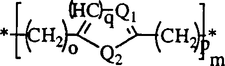
- c) eine Kette der allgemeinen Formel III wobei o und p unabhängig voneinander 0 oder eine ganze Zahl von 1 bis 3 sein können, m eine ganze Zahl von 1 bis 5 ist, q 1 oder 2 ist und Q1 und Q2 unabhängig voneinander CH, O, S oder N(H) ist und insbesondere die Reste Phenyl, Biphenyl, Tertphenyl, Quartphenyl, (Oligo)thiophen, (Oligo)pyrrol, (Oligo)imidazol, (Oligo)pyridin oder (Oligo)pyrazin oder eine Kombination aus a) und b), aus c) oder aus a), b) und c) auf, wobei M H, ein organischer Rest oder ein Metall kation) ist.
the rest R, selected from the group consisting of:
- a) an alkyl chain having 2 to 20 carbon atoms, which may be linear or branched and / or substituted and / or contains unsaturated bond, with particular preference is an n-alkyl chain of the formula - (CH 2 ) X -CH 3 , wherein x is an integer between 1 and 19;
- b) Oligothioetherkette the general formula II
- c) a chain of general formula III wherein o and p independently of one another may be 0 or an integer of 1 to 3, m is an integer of 1 to 5, q is 1 or 2 and Q1 and Q2 are independently CH, O, S or N (H) and in particular the radicals phenyl, biphenyl, tert-phenyl, quartophenyl, (oligo) thiophene, (oligo) pyrrole, (oligo) imidazole, (oligo) pyridine or (oligo) pyrazine or a combination of a) and b), from c) or from a), b) and c), wherein MH, an organic radical or a metal cation) is.
Im Allgemeinen eignen sich alle organischen Reste, die bewegliche oder starre lineare Einheiten mit den unter a), b) und c) aufgeführten Gruppen bilden. Die Länge des Restes bestimmt nicht nur die Flexibilität und die Ausrichtung der selbstorganisierten Monolage sondern auch die Dicke der Isolationsschicht und somit die Größe der Versorgungsspannung im Bauelement. Eine geeignete Kombination von linearen, flexiblen und aromatischen bzw. heteroaromatischen Molekülfragmenten im organischen Rest kann sogar zu einer Verbesserung der Schichteigenschaften beitragen und zwar in der Weise, dass durch den Einbau von aromatischen bzw. heteroaromatischen Gruppen eine Stabilisierung der Schicht erreicht wird, welche auf der ππ-Wechselwirkung gleicher Gruppen benachbarter Ketten beruht. Neben der oben genannten Gruppen können auch weitere Gruppen im organischen Rest vorhanden sein, um einerseits die Ausrichtung des Moleküls zu bestimmen und andererseits zu einer Stabilisierung durch Wechselwirkungen, wie z. B. Dipol-Dipol, CT-Wechselwirkungen, ππ-Wechselwirkungen oder durch eine Stabilisierung durch die van der Waals-Kräfte. Die erfindungsgemäßen Materialien richten sich dabei in der Weise auf der Oberfläche der Gateelektrode aus, dass die Phosphonsäuregruppe als Ankergruppe in möglichst dichter Weise die oxidische Substratoberfläche besetzt und die linearen organischen Reste sich parallel zu benachbarten Resten von der Substratoberfläche weg anordnet. Die parallele Ausrichtung der organischen Reste erfolgt im Allgemeinen nicht orthogonal zum Substrat sondern unter Ausbildung eines Winkels, wobei die Größe des Winkels nicht entscheidend ist.in the In general, all organic radicals that are mobile or rigid linear units with the groups listed under a), b) and c) form. The length the rest not only determines the flexibility and the orientation of the self-organized Monolayer but also the thickness of the insulation layer and thus the size of the supply voltage in the component. A suitable combination of linear, flexible and aromatic or heteroaromatic molecule fragments in the organic radical can even contribute to an improvement of the coating properties in such a way that by the incorporation of aromatic or heteroaromatic groups achieved a stabilization of the layer which is the same on the ππ interaction Groups of adjacent chains based. In addition to the above groups can Also, additional groups may be present in the organic residue, on the one hand the orientation of the molecule and on the other hand to a stabilization through interactions, such as As dipole-dipole, CT interactions, ππ interactions or by a stabilization by the van der Waals forces. Direct the materials according to the invention doing so in the way on the surface of the gate electrode, that the phosphonic acid group as Anchor group in as possible densely occupied the oxidic substrate surface and the linear organic residues are parallel to adjacent residues away from the substrate surface arranges. The parallel alignment of the organic radicals takes place in Generally not orthogonal to the substrate but under training an angle, where the size of the angle is not crucial.
Die Stärke der selbstorganisierten Monolage (Schichtdicke) wird durch die Länge des organischen Moleküls bestimmt. In einer besonders bevorzugten Ausführungsform weist die Dielektrikumsschicht eine Stärke von etwa 1 bis etwa 10 nm, vorzugsweise von etwa 2 bis etwa 5 nm auf.The Strength of the self - assembled monolayer (layer thickness) is determined by the length of the organic molecule certainly. In a particularly preferred embodiment, the dielectric layer a strength from about 1 to about 10 nm, preferably from about 2 to about 5 nm on.
Als Materialien für die Gateelektrode, eignen sich im Prinzip alle Materialien, die entweder eine native Oxidschicht aufweisen, die mit den Phosphonsäure-Gruppen eine Wechselwirkung eingehen. In einer besonderen Ausführungsform weist die Ober fläche der Gateelektrode eine Metalloxidschicht auf. Es ist aber anzumerken, dass auch andere Metallschichten mit den Phosphonsäuregruppen eine Wechselwirkung eingehen können, was zur Ausbildung einer selbstorganisierten Monolage führt. Solche Oberflächen können zum Beispiel Hydroxyoxidoberflächen sein.When Materials for the gate electrode, in principle, are all materials that either a native oxide layer having the phosphonic acid groups to interact. In a particular embodiment has the upper surface the gate electrode has a metal oxide layer. It should be noted, however, that other metal layers with the phosphonic acid groups to be able to interact which leads to the formation of a self-organized monolayer. Such surfaces can for example, hydroxy oxide surfaces be.
Die bevorzugten Materialien für die Gateelektrode sind Aluminium (Al), Titan (Ti), Titanitrid (TiN), Tantal (Ta), Tantalnitrid (TaN), Wolfram (W), Titanwolfram (TiW), Tantalwolfram (TaW), Wolframnitrid (WN), Wolframcarbonitrid (WCN), Irridiumoxid (IrO), Rutheniumoxid (RuO), Strontiumrutheniumoxid (SrRuO) bzw. eine Kombination dieser Schichten und/oder Materialien. Die Gateelektrode weist gegebenenfalls zusätzlich auch eine Schicht aus Silizium (Si), Titannitridsilizium (TiNSi), Siliziumoxynitrid (SiON), Siliziumoxid (SiO), Siliziumcarbid (SiC) oder Siliziumcarbonitrid (SiCN) auf. Wenn das Elektrodenmaterial keine native Oxidschicht aufweist, kann die Oberfläche gezielt behandelt werden, um entweder eine Oxidschicht oder eine andere Schicht zu erhalten, die mit den Phosphonsäuregruppen eine Wechselwirkung eingehen.The preferred materials for the gate electrode are aluminum (Al), titanium (Ti), titanium nitride (TiN), tantalum (Ta), tantalum nitride (TaN), tungsten (W), titanium tungsten (TiW), tantalum tungsten (TaW), tungsten nitride (WN ), Tungsten carbonitride (WCN), irridium oxide (IrO), ruthenium oxide (RuO), strontium ruthenium oxide (SrRuO) or a combination of these layers and / or materials. Optionally, the gate electrode additionally has a layer of silicon (Si), titanium nitride silicon (TiNSi), silicon oxynitride (SiON), silicon oxide (SiO), silicon carbide (SiC) or silicon carbonitride (SiCN). If the electrode material does not have a native oxide layer, the surface may be selectively treated to receive either an oxide layer or another layer which interact with the phosphonic acid groups.
Es ist lediglich notwendig, dass die Oberfläche der Gateelektrode so gestaltet ist, dass eine Wechselwirkung mit Phosphonsäuregruppen möglich ist.It is only necessary that the surface of the gate electrode designed so is that an interaction with phosphonic acid groups is possible.
Die Materialien für die Source- und Drainelektrode sind für die Funktion des Bauelementes in der Weise nicht entscheidend, da keine direkte Wechselwirkung (Anbindung etc.) der erfindungsgemäßen Phosphonsäureverbindungen besteht. Prinzipiell eignen sich alle leitfähigen Metalle, Formulierungen dieser oder Polymere. Beispielsweise werden folgende Materialien genannt: Gold (Au), Silber (Ag), Kupfer (Cu), Titan (Ti), Titannitrid (TiN), Tantal (Ta), Tantalnitrid (TaN), Wolfram (W), Titanwolfram (TiW), Tantalwolfram (TaW), Wolframnitrid (WN), Wolframcarbonitrid (WCN), Irridiumoxid, Rutheniumoxid, Strontiumrutheniumoxid, Platin, Palladium, Gal liumarsenid usw. Auch die Source- bzw. Drainelektrode können zusätzlich eine Schicht aus Si, TiNSi, SiON, SiO, SiC oder SiCN aufweisen. Als polymere Kontaktmaterialien sind beispielsweise PEDOT:PSS (Baytron®)oder Polyanilin geeignet.The materials for the source and drain electrodes are not critical to the function of the device, as there is no direct interaction (attachment, etc.) of the phosphonic acid compounds of the invention. In principle, all conductive metals, formulations of these or polymers are suitable. For example, the following materials are named: gold (Au), silver (Ag), copper (Cu), titanium (Ti), titanium nitride (TiN), tantalum (Ta), tantalum nitride (TaN), tungsten (W), titanium tungsten (TiW). , Tantalum tungsten (TaW), tungsten nitride (WN), tungsten carbonitride (WCN), irridium oxide, ruthenium oxide, strontium ruthenium oxide, platinum, palladium, gallium arsenide, etc. The source or drain electrode may additionally comprise a layer of Si, TiNSi, SiON, SiO, SiC or SiCN have. Useful polymeric contact materials are for example PEDOT: PSS (Baytron ®) or polyaniline suitable.
Die erfindungsgemäße Dielektrikumsschicht aus einer organischen Verbindung mit Phosphonsäuregruppen eignet sich insbesondere dann, wenn ein Halbleitermaterial verwendet wird, das auf der Basis eines organischen Halbleiters ausgebildet ist. Der Begriff Phosphorsäuregruppe ist so zu verstehen, dass auch Phosporsäure-Derivate wie z. B. FsW oder Salze darunter verstanden werden sollen.The inventive dielectric layer an organic compound having phosphonic acid groups is particularly suitable when a semiconductor material is used based on a organic semiconductor is formed. The term phosphoric acid group is to be understood that also phosphoric acid derivatives such. B. FsW or Salts should be understood.
In einer besonderen Ausführungsform wird das Halbleitermaterial auf der Basis eines organischen Halbleiters aufgebaut. Der organische Halbleiter kann zum Beispiel aus der Gruppe, bestehend aus Pentazen, Tetrazen und Oligothiophen ausgewählt werden.In a particular embodiment becomes the semiconductor material based on an organic semiconductor built up. The organic semiconductor may, for example, be selected from the group consisting of pentacene, tetracene and oligothiophene.
Die Versorgungsspannung eines Feldeffekttransistors hängt insbesondere von der Stärke der auf der Gateelektrode angeordneten Dielektrikumsschicht (des Gatedielektrikums) ab. Deshalb kann der erfindungsgemäße Feldeffekttransistor mit einer Versorgungsspannung von weniger als 5 Volt und insbesondere von weniger als 3 Volt, nämlich im Bereich von 1 bis 3 Volt betrieben werden.The Supply voltage of a field effect transistor depends in particular of the strength the dielectric layer (the Gate dielectric). Therefore, the field effect transistor according to the invention with a supply voltage of less than 5 volts and in particular less than 3 volts, viz be operated in the range of 1 to 3 volts.
Falls aber eine höhere Versorgungsspannung gewünscht ist, kann auf die Oberfläche der selbstorganisierten Monolage beispielsweise eine inorganische oder organische Isolationsschicht aufgebracht werden. Wenn die Isolationsschicht auf Basis zum Beispiel eines organischen Polymers ausgebildet ist, weist diese Schicht eine Stärke von 10 bis 30 nm auf.If but a higher one Supply voltage desired is, can on the surface the self-assembled monolayer, for example, an inorganic or organic insulating layer are applied. If the insulation layer formed on the basis of, for example, an organic polymer, this layer has a strength from 10 to 30 nm.
Die erfindungsgemäßen Feldeffekttransistoren eignen sich insbesondere zur Verwendung im so genannten "Low Cost"-Be reich der Elektronik und speziell für organische Feldeffekttransistoren mit niedrigen Versorgungsspannungen.The Field effect transistors according to the invention are particularly suitable for use in the so-called "low cost" -Be rich electronics and especially for organic field-effect transistors with low supply voltages.
In einem Aspekt der Erfindung wird ein Herstellungsverfahren bereitgestellt, zur Herstellung von Feldeffekttransistoren.In In one aspect of the invention, a manufacturing method is provided. for the production of field effect transistors.
In dem erfindungsgemäßen Verfahren, wird ein Substrat auf der Basis von inorganischen oder organischen Materialien bereitgestellt, worauf eine Gateelektrode abgeschieden wird. Die Gateelektrode kann dann mit einer organischen Verbindung, die eine Phosphonsäuregruppe aufweist, in Kontakt gebracht werden, um eine auf der Gateelektrode angeordnete selbstorganisierte Monolage der organischen Verbindung zu erhalten. Wie vorstehend beschrieben, weist die Oberfläche der Gateelektrode solche Eigenschaften auf, dass die Phosphonsäuregruppe mit der Oberfläche der Gateelektrode eine Wechselwirkung eingeht. Eine so erhaltene selbstorganisierte Monolage der organischen Verbindung kann dann weiteren Herstellungsschritten unterzogen werden. In dem erfindungsgemäßen Verfahren wird daher als nächster Schritt das Abscheiden und Strukturieren einer Source- und einer Drainelektrode mit dem nachfolgenden Abscheiden eines Halbleitermaterials vorgesehen.In the method according to the invention, becomes a substrate based on inorganic or organic Materials are provided, whereupon a gate electrode is deposited becomes. The gate electrode can then be filled with an organic compound, the one phosphonic acid group has to be brought into contact with one on the gate electrode arranged self-assembled monolayer of the organic compound to obtain. As described above, the surface of the Gate electrode has such properties that the phosphonic acid group with the surface the gate electrode enters into an interaction. Such a preserved Self-assembled monolayer of the organic compound can then be subjected to further manufacturing steps. In the method according to the invention is therefore next Step the deposition and structuring of a source and a Drain electrode with the subsequent deposition of a semiconductor material intended.
Das in Kontakt bringen der organischen Verbindung mit dem Material der Gateelektrode kann entweder dadurch erfolgen, dass ein Substrat mit der daran angeordneten Gateelektrode in eine Lösung eingetaucht wird, die die erfindungsgemäße organische Verbindung aufweist.The contact the organic compound with the material of the Gate electrode can either be done by a substrate immersed in a solution with the gate electrode arranged thereon is, which is the inventive organic Compound has.
Als Lösungsmittel eignen sich insbesondere protische, polare Lösungsmittel, wie zum Beispiel Alkohol.When solvent In particular, protic, polar solvents, such as, for example, are suitable Alcohol.
Die Dichte der selbstorganisierten Monolage der organischen Verbindung und die Dauer der Abscheidung kann durch die Konzentration der Lösung der organischen Verbindung in die das Substrat eingetaucht wird, beeinflusst werden. Die Konzentration der Lösung im Bereich von etwa 10–4 bis 0,1 mol-% der organischen Verbindung eigner sich besonders zur Herstellung dichter Schichten. Nachdem das Substrat in die Lösung der organischen Verbindung eingetaucht wurde, kann anschließend ein Spülschritt mit reinem Prozesslösungsmittel erfolgen. Danach kann gegebenenfalls das Substrat mit einem leicht flüchtigen Lösungsmittel wie zum Beispiel Aceton oder Dichlormethan gespült werden und abschließend getrocknet. Das Trocknen kann zum Beispiel im Ofen oder auf einer Hot-Plate unter Schutzgas erfolgen.The density of the self-assembled monolayer of the organic compound and the duration of the deposition can be influenced by the concentration of the solution of the organic compound into which the substrate is immersed. The concentration of the solution in the range of about 10 -4 to 0.1 mol% of the organic compound is particularly suitable for producing dense layers. After the substrate has been immersed in the organic compound solution, a pure process solvent rinse step can then be performed. Thereafter, if necessary, the substrate may be rinsed with a volatile solvent such as acetone or dichloromethane and finally dried. The drying can take place, for example, in the oven or on a hot plate under protective gas.
Die organische Verbindung kann aber auch durch Aufdampfen der organischen Verbindung auf die Gateelektrode mit der Gateelektrode in Kontakt gebracht werden.The Organic compound can also by evaporation of the organic Connection to the gate electrode brought into contact with the gate electrode become.
Das Abscheiden der organischen Verbindung kann dann in einem geschlossenen Reaktor mit Heizung erfolgen. Der Reaktorinnenraum wird nach der Beladung mit dem Substrat mit definierter Gateelektrode evakuiert und mit Inertgas wie zum Beispiel Argon oder Stickstoff belüftet, um Reste von Sauerstoff zu entfernen. Anschließend werden Arbeitsdruck und Arbeitstemperatur angestellt, die sich im Wesentlichen nach dem organischen Rest richten. Ein Druck von etwa 10–6 bis 400 mbar und eine Temperatur von etwa 80 bis 200°C sind besonders bevorzugt. Die idealen Prozessbedingungen richten sich nach der Flüchtigkeit der organischen Verbindung. Die Beschichtungszeiten betragen in der Regel je nach Prozessbedingungen zwischen 3 min und 24 h.The deposition of the organic compound can then take place in a closed reactor with heating. The reactor interior is evacuated after loading with the substrate with a defined gate electrode and aerated with inert gas such as argon or nitrogen to remove residues of oxygen. Subsequently, working pressure and working temperature are set, which essentially depend on the organic residue. A pressure of about 10 -6 to 400 mbar and a temperature of about 80 to 200 ° C are particularly preferred. The ideal process conditions depend on the volatility of the organic compound. The coating times are usually between 3 minutes and 24 hours depending on the process conditions.
Eine der Aufgaben wird durch die Verwendung einer organischen Verbindung, die eine Phosphonsäuregruppe aufweist, bei der Herstellung von Feldeffekttransistoren gelöst.A The tasks are accomplished through the use of an organic compound, the one phosphonic acid group has dissolved in the production of field effect transistors.
In einer besonderen Ausführungsform bildet die organische Verbindung mit der Phosphonsäuregruppe auf der Gateelektrode eine selbstorganisierte Monolage aus.In a particular embodiment forms the organic compound with the phosphonic acid group on the gate electrode from a self-assembled monolayer.
Dabei dient die organische Verbindung mit der Phosphonsäuregruppe als Gatedielektrikum.there the organic compound serves with the phosphonic acid group as a gate dielectric.
Die Erfindung wird nun anhand der Figuren näher erläutert.The The invention will now be explained in more detail with reference to FIGS.
Es zeigt:It shows:
Die
elektronischen Eigenschaften des erfindungsgemäßen Feldeffekttransistors sind
in
- 11
- Gateelektrodegate electrode
- 22
- Monolage der organischen Verbindungmonolayer the organic compound
- 33
- Substratsubstratum
- 44
- Sourceelektrodesource electrode
- 55
- Halbleitersemiconductor
- 66
- Drainelektrodedrain
Claims (21)
Priority Applications (2)
| Application Number | Priority Date | Filing Date | Title |
|---|---|---|---|
| DE102004009600A DE102004009600B4 (en) | 2004-02-27 | 2004-02-27 | Self-organizing organic dielectric layers based on phosphonic acid derivatives |
| US11/066,617 US20050189536A1 (en) | 2004-02-27 | 2005-02-28 | Self-assembly organic dielectric layers based on phosphonic acid derivatives |
Applications Claiming Priority (1)
| Application Number | Priority Date | Filing Date | Title |
|---|---|---|---|
| DE102004009600A DE102004009600B4 (en) | 2004-02-27 | 2004-02-27 | Self-organizing organic dielectric layers based on phosphonic acid derivatives |
Publications (2)
| Publication Number | Publication Date |
|---|---|
| DE102004009600A1 true DE102004009600A1 (en) | 2005-09-22 |
| DE102004009600B4 DE102004009600B4 (en) | 2008-04-03 |
Family
ID=34877158
Family Applications (1)
| Application Number | Title | Priority Date | Filing Date |
|---|---|---|---|
| DE102004009600A Expired - Fee Related DE102004009600B4 (en) | 2004-02-27 | 2004-02-27 | Self-organizing organic dielectric layers based on phosphonic acid derivatives |
Country Status (2)
| Country | Link |
|---|---|
| US (1) | US20050189536A1 (en) |
| DE (1) | DE102004009600B4 (en) |
Cited By (6)
| Publication number | Priority date | Publication date | Assignee | Title |
|---|---|---|---|---|
| WO2005109538A2 (en) * | 2004-05-07 | 2005-11-17 | Qimonda Ag | Ultra-thin dielectric and use thereof in organic field-effect transistors |
| WO2006058858A2 (en) * | 2004-11-30 | 2006-06-08 | Qimonda Ag | Method for synthesizing long-chain phosphonic acid derivatives and thiol derivatives |
| DE102006049432A1 (en) * | 2006-10-16 | 2008-04-17 | Philipps-Universität Marburg | Process for the preparation of self-aggregating monolayers on solid surfaces |
| DE102009037691A1 (en) * | 2009-08-17 | 2011-03-03 | Siemens Aktiengesellschaft | Dielectric protective layer for a self-assembling monolayer (SAM) |
| US8614875B2 (en) | 2008-09-23 | 2013-12-24 | Siemens Aktiengesellschaft | Anchor group for monolayers of organic compounds on metal and component produced therewith by means of organic electronics |
| DE102013202252A1 (en) * | 2013-02-12 | 2014-08-28 | Siemens Aktiengesellschaft | Thin-film capacitors with high integration density |
Families Citing this family (14)
| Publication number | Priority date | Publication date | Assignee | Title |
|---|---|---|---|---|
| WO2006098416A1 (en) * | 2005-03-15 | 2006-09-21 | Pioneer Corporation | Organic thin-film transistor and method for manufacturing same |
| KR100708720B1 (en) * | 2005-10-19 | 2007-04-17 | 삼성에스디아이 주식회사 | A organic thin film transistor, a method for preparing the same and a flat panel display comprising the same |
| KR100719566B1 (en) * | 2005-10-22 | 2007-05-17 | 삼성에스디아이 주식회사 | An organic thin film transistor, and a flat panel display therewith |
| WO2007099690A1 (en) * | 2006-02-28 | 2007-09-07 | Pioneer Corporation | Organic transistor and method for manufacturing same |
| JP4379450B2 (en) * | 2006-08-22 | 2009-12-09 | ソニー株式会社 | Electronic device and manufacturing method thereof |
| KR101249090B1 (en) * | 2006-11-14 | 2013-03-29 | 삼성전자주식회사 | Composition for Preparing Organic Insulator and the Organic Insulator prepared by using the same |
| DE102007029837A1 (en) | 2007-06-28 | 2009-01-02 | Siemens Ag | Additive, useful e.g. in a cleaning or care-product, which is in the form of a compound formed as linear molecule having a molecular chain and an anchoring group, which binds to a metallic surface and forms a monomolecular layer |
| DE102007029836A1 (en) | 2007-06-28 | 2009-01-02 | Siemens Ag | Additive, useful e.g. in a cleaning or care-product, which is in the form of a compound formed as linear molecule having a molecular chain and an anchoring group, which binds to a metallic surface and forms a monomolecular layer |
| DE102007046444A1 (en) * | 2007-09-28 | 2009-04-02 | Siemens Ag | Organic photodetector with reduced dark current |
| DE102009023350A1 (en) | 2009-05-29 | 2010-12-02 | Osram Opto Semiconductors Gmbh | Electronic component and method for producing an electronic component |
| US9299941B2 (en) * | 2011-01-13 | 2016-03-29 | Samsung Electronics Co., Ltd. | Organic semiconductor device and method of manufacturing the same |
| US8124485B1 (en) | 2011-02-23 | 2012-02-28 | International Business Machines Corporation | Molecular spacer layer for semiconductor oxide surface and high-K dielectric stack |
| KR102450399B1 (en) * | 2015-10-06 | 2022-09-30 | 삼성전자주식회사 | Thin film transistor, method of manufacturing same, and electronic device including thin same |
| US20220045274A1 (en) * | 2020-08-06 | 2022-02-10 | Facebook Technologies Llc | Ofets having organic semiconductor layer with high carrier mobility and in situ isolation |
Family Cites Families (10)
| Publication number | Priority date | Publication date | Assignee | Title |
|---|---|---|---|---|
| US5892244A (en) * | 1989-01-10 | 1999-04-06 | Mitsubishi Denki Kabushiki Kaisha | Field effect transistor including πconjugate polymer and liquid crystal display including the field effect transistor |
| US5946551A (en) * | 1997-03-25 | 1999-08-31 | Dimitrakopoulos; Christos Dimitrios | Fabrication of thin film effect transistor comprising an organic semiconductor and chemical solution deposited metal oxide gate dielectric |
| US6344662B1 (en) * | 1997-03-25 | 2002-02-05 | International Business Machines Corporation | Thin-film field-effect transistor with organic-inorganic hybrid semiconductor requiring low operating voltages |
| JP2000269504A (en) * | 1999-03-16 | 2000-09-29 | Hitachi Ltd | Semiconductor device, its manufacture and liquid crystal display device |
| WO2001097297A1 (en) * | 2000-06-16 | 2001-12-20 | The Penn State Research Foundation | Aqueous-based photolithography on organic materials |
| US7141644B2 (en) * | 2002-01-11 | 2006-11-28 | Xerox Corporation | Polthiophenes and devices thereof |
| US7285440B2 (en) * | 2002-11-25 | 2007-10-23 | International Business Machines Corporation | Organic underlayers that improve the performance of organic semiconductors |
| US6869821B2 (en) * | 2002-12-30 | 2005-03-22 | Xerox Corporation | Method for producing organic electronic devices on deposited dielectric materials |
| DE10328810B4 (en) * | 2003-06-20 | 2005-10-20 | Infineon Technologies Ag | A synthesis method of a compound for forming a self-assembling monolayer, a compound for forming a self-assembling monolayer, and a layer structure for a semiconductor device |
| DE10328811B4 (en) * | 2003-06-20 | 2005-12-29 | Infineon Technologies Ag | A compound for forming a self-assembling monolayer, a layered structure, a semiconductor device having a layered structure and a method for producing a layered structure |
-
2004
- 2004-02-27 DE DE102004009600A patent/DE102004009600B4/en not_active Expired - Fee Related
-
2005
- 2005-02-28 US US11/066,617 patent/US20050189536A1/en not_active Abandoned
Non-Patent Citations (4)
| Title |
|---|
| Halik, M. et al.: "Relationsship between molecular and electrical performance of oligothiophene or- ganic thin film transistors". In: Adv.Mater., 5 June 2003, Vol.15, No.11, pp.917-922 |
| Halik, M. et al.: "Relationsship between molecularand electrical performance of oligothiophene or- ganic thin film transistors". In: Adv.Mater., 5 June 2003, Vol.15, No.11, pp.917-922 * |
| Ulman, A. et al.: "Formation and Structure of Self -Assembled Monolayers". In: Chem. Rev., 1996, Vol. 96,No.4, pp.1533-1554 |
| Ulman, A. et al.: "Formation and Structure of Self-Assembled Monolayers". In: Chem. Rev., 1996, Vol.96,No.4, pp.1533-1554 * |
Cited By (13)
| Publication number | Priority date | Publication date | Assignee | Title |
|---|---|---|---|---|
| WO2005109538A3 (en) * | 2004-05-07 | 2006-09-08 | Infineon Technologies Ag | Ultra-thin dielectric and use thereof in organic field-effect transistors |
| WO2005109538A2 (en) * | 2004-05-07 | 2005-11-17 | Qimonda Ag | Ultra-thin dielectric and use thereof in organic field-effect transistors |
| WO2006058858A2 (en) * | 2004-11-30 | 2006-06-08 | Qimonda Ag | Method for synthesizing long-chain phosphonic acid derivatives and thiol derivatives |
| WO2006058858A3 (en) * | 2004-11-30 | 2006-09-21 | Infineon Technologies Ag | Method for synthesizing long-chain phosphonic acid derivatives and thiol derivatives |
| DE102006049432A1 (en) * | 2006-10-16 | 2008-04-17 | Philipps-Universität Marburg | Process for the preparation of self-aggregating monolayers on solid surfaces |
| US8842414B2 (en) | 2008-09-23 | 2014-09-23 | Siemens Aktiengesellschaft | Anchor group for monolayers of organic compounds on metal and component produced therewith by means of organic electronics |
| EP2706585A3 (en) * | 2008-09-23 | 2017-01-25 | Siemens Aktiengesellschaft | Component based on organic electronics |
| US8614875B2 (en) | 2008-09-23 | 2013-12-24 | Siemens Aktiengesellschaft | Anchor group for monolayers of organic compounds on metal and component produced therewith by means of organic electronics |
| EP2326746B1 (en) * | 2008-09-23 | 2014-04-16 | Siemens Aktiengesellschaft | Anchor group for monolayers of organic compounds on metal and component produced therewith by means of organic electronics |
| DE102009037691A8 (en) * | 2009-08-17 | 2011-06-01 | Siemens Aktiengesellschaft | Dielectric protective layer for a self-assembling monolayer (SAM) |
| US8945297B2 (en) | 2009-08-17 | 2015-02-03 | Siemens Aktiengesellschaft | Dielectric protective layer for a self-organizing monolayer (SAM) |
| DE102009037691A1 (en) * | 2009-08-17 | 2011-03-03 | Siemens Aktiengesellschaft | Dielectric protective layer for a self-assembling monolayer (SAM) |
| DE102013202252A1 (en) * | 2013-02-12 | 2014-08-28 | Siemens Aktiengesellschaft | Thin-film capacitors with high integration density |
Also Published As
| Publication number | Publication date |
|---|---|
| DE102004009600B4 (en) | 2008-04-03 |
| US20050189536A1 (en) | 2005-09-01 |
Similar Documents
| Publication | Publication Date | Title |
|---|---|---|
| DE102004009600B4 (en) | Self-organizing organic dielectric layers based on phosphonic acid derivatives | |
| WO2005109538A2 (en) | Ultra-thin dielectric and use thereof in organic field-effect transistors | |
| DE10328811B4 (en) | A compound for forming a self-assembling monolayer, a layered structure, a semiconductor device having a layered structure and a method for producing a layered structure | |
| DE10006257B4 (en) | Thin-film transistors with organic-inorganic hybrid materials as semiconducting channels | |
| EP2436057B1 (en) | Electronic component and method for producing an electronic component | |
| DE102004025423B4 (en) | Thin-film field-effect transistor with gate dielectric of organic material and method for its production | |
| EP1702369A1 (en) | Semiconductor arrangement with non-volatile memories | |
| EP1516374A1 (en) | Reduction in the contact resistance in organic field effect transistors with palladium contacts by the use of nitriles and isonitriles | |
| DE102012200896A1 (en) | Electronic component | |
| DE10151036A1 (en) | Isolator for an organic electronic component | |
| DE102006003572A1 (en) | Hybrid silicon-molecular memory cell based on Fc-BzCN and Por-BzCN molecular complexes | |
| DE102004010094B3 (en) | Semiconductor device having at least one organic semiconductor layer and method for its production | |
| DE102004008784B3 (en) | Process for the through-contacting of field effect transistors with a self-assembled monolayer of an organic compound as a gate dielectric | |
| DE102004009601B4 (en) | Method for producing a field effect transistor | |
| EP1704606B1 (en) | Method for the production of an organic transistor comprising a self-adjusting gate electrode | |
| EP1644995B1 (en) | Semiconductor component, and method for the production thereof | |
| DE10340610B4 (en) | Connection with at least one storage unit made of organic storage material, in particular for use in CMOS structures, semiconductor component and a method for producing a semiconductor component | |
| EP1803173B1 (en) | Method for the production of a semi-conductor component by means of inorganic-organic hybrid polymers | |
| DE102005005589A1 (en) | Hybrid organic thin layered field effect transistor for use in polymer circuit, has source and drain electrodes including thin copper layer whose surface area facing semiconductor layer is modified to form copper oxide layer between layers | |
| DE102004026108B4 (en) | Integrated semiconductor circuit arrangement and method for its production | |
| DE102005048774B4 (en) | Substrate, which is at least partially provided on a surface with a coating of a metal, and its use | |
| EP1771897A1 (en) | Method for forming memory layers |
Legal Events
| Date | Code | Title | Description |
|---|---|---|---|
| OP8 | Request for examination as to paragraph 44 patent law | ||
| 8127 | New person/name/address of the applicant |
Owner name: QIMONDA AG, 81739 MUENCHEN, DE |
|
| 8364 | No opposition during term of opposition | ||
| R081 | Change of applicant/patentee |
Owner name: POLARIS INNOVATIONS LTD., IE Free format text: FORMER OWNER: QIMONDA AG, 81739 MUENCHEN, DE Owner name: INFINEON TECHNOLOGIES AG, DE Free format text: FORMER OWNER: QIMONDA AG, 81739 MUENCHEN, DE |
|
| R081 | Change of applicant/patentee |
Owner name: POLARIS INNOVATIONS LTD., IE Free format text: FORMER OWNER: INFINEON TECHNOLOGIES AG, 85579 NEUBIBERG, DE |
|
| R119 | Application deemed withdrawn, or ip right lapsed, due to non-payment of renewal fee |