CN203446121U - Printed circuit board through hole tool - Google Patents
Printed circuit board through hole tool Download PDFInfo
- Publication number
- CN203446121U CN203446121U CN201320557548.7U CN201320557548U CN203446121U CN 203446121 U CN203446121 U CN 203446121U CN 201320557548 U CN201320557548 U CN 201320557548U CN 203446121 U CN203446121 U CN 203446121U
- Authority
- CN
- China
- Prior art keywords
- hole
- perforation
- circuit board
- printed circuit
- printing table
- Prior art date
- Legal status (The legal status is an assumption and is not a legal conclusion. Google has not performed a legal analysis and makes no representation as to the accuracy of the status listed.)
- Withdrawn - After Issue
Links
Images

Abstract
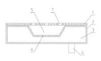
Provided is a printed circuit board through hole tool which comprises a through hole printing template and a through hole printing table. The through hole printing template is fixed on the upper surface of the through hole printing table. The internal part of the through hole printing table is a hollow cavity. The bottom part of the through hole printing table is provided with an exhaust inlet used for absorbing vacuum. The middle of the upper surface of the through hole printing table is provided with a trapezoid-shaped groove which dents inwardly. A negative pressure cavity is formed by the through hole printing template and the trapezoid-shaped groove. The bottom part of the trapezoid-shaped groove is provided with through holes which are communicated with the cavity. The through hole printing template is provided with mould holes which are arranged within the range of the upper surface of the trapezoid-shaped groove. The beneficial effects of the printed circuit board through hole tool are that: the through hole tool is manufactured by using organic glass, and existing through hole equipment is improved so that the printed circuit board through hole tool is low in cost, easy to manufacture and convenient and practical, and thus quality of printed circuit board through hole products is substantially enhanced.
Description
Technical field
This utility model relates to a kind of printed circuit board (PCB) perforation tool, particularly a kind of bad perforation tool of perforation plug-hole that solves for carbon slurry perforation, when silver paste hole filled.
Background technology
Traditional carbon slurry perforation, silver paste hole filled silk-screen, rely on the self-contained vacuum pump of screen printing device to vacuumize, and the ink on screen cloth is sucked and needed in the hole of perforation, forms via.Because not every hole in a carbon slurry perforation product or silver paste hole filled product all needs to carry out perforation operation, but also necessary moulding of these holes before perforation, this has just disperseed the suction of vacuum pump, easily cause ink to be blocked in hole, cause the obstructed or poor flow in hole, thereby cause scrapping of substrate.And the expense of a vacuum pump of reforming equipment increase is higher, and on obstructed product, the quantity in hole is inconsistent, needs the quantity of perforation also inconsistent, has caused the increase of vacuum pump might not play expected effect.
Summary of the invention
Goal of the invention: the purpose of this utility model is to provide and a kind ofly can improves silk-screen perforation quality, printed circuit board (PCB) perforation tool simple to operate.
Technical scheme: a kind of printed circuit board (PCB) perforation tool, comprise perforation printing stencil and perforation printing table, described perforation printing stencil is fixed on perforation printing table upper surface, described perforation printing table inside is the shape chamber of hollow, described perforation printing table bottom is provided with the inlet scoop of inhaling vacuum, in the middle of described perforation printing table upper surface, be provided with the dovetail groove of indent, described perforation printing stencil and dovetail groove form airtight negative pressure shape chamber, described dovetail groove bottom is provided with the through hole that is communicated with shape chamber, described perforation printing stencil is provided with die hole, described die hole is positioned at dovetail groove upper surface scope.Owing to needing the hole of perforation on the equal corresponding circuits base board of the die hole on perforation printing stencil, hole on perforation printing table and perforation printing stencil forms funnel type, increased suction, and do not need the hole of perforation on perforation printing stencil, not hole, and avoided the dispersion of suction, improved the suction of perforation, use the ink of perforation can run through easily substrate, and be attached on hole wall uniformly, aperture opening ratio is higher, and hole wall is more smooth.When saving production cost, improved product quality.
In order to improve the efficiency of perforation operation, on described perforation printing stencil, be also provided with location hole.Need to carry out location hole on the circuit board substrate of perforation and the overlapping realization of location hole on perforation printing stencil accurately locates.
In order further to reduce costs, the material of described perforation printing stencil is polymethyl methacrylate.
Beneficial effect: the utility model, by using polymethyl methacrylate to manufacture perforation tool, improves existing perforation equipment, with low cost, makes simply, convenient and practical, has significantly improved the quality of printed circuit board (PCB) perforation product.
Accompanying drawing explanation
Fig. 1 is structural representation of the present utility model;
Fig. 2 is the front view of the utility model perforation printing stencil.
Embodiment
Below in conjunction with accompanying drawing, the utility model is described in further detail.
As shown in Figure 1, a kind of printed circuit board (PCB) perforation tool, comprise perforation printing stencil 1 and perforation printing table 2, described perforation printing stencil 1 is fixed on perforation printing table 2 upper surfaces, described perforation printing table 2 inside are the shape chamber 3 of hollow, described perforation printing table 2 bottoms are provided with the inlet scoop 4 of inhaling vacuum, in the middle of described perforation printing table 2 upper surfaces, be provided with the dovetail groove 5 of indent, described perforation printing stencil 1 forms airtight negative pressure shape chamber with dovetail groove 5, described dovetail groove 5 bottoms are provided with the through hole 6 that is communicated with shape chamber 3, described perforation printing stencil 1 is provided with die hole 7, described die hole 7 is positioned at dovetail groove 5 upper surface scopes.Owing to needing the hole of perforation on the equal corresponding circuits base board of die hole 7 on perforation printing stencil 1, perforation printing table 2 forms funnel type with the hole on perforation printing stencil 1, increased suction, and do not need the hole of perforation on perforation printing stencil 1, not hole, and avoided the dispersion of suction, improved the suction of perforation, use the ink of perforation can run through easily substrate, and be attached on hole wall uniformly, aperture opening ratio is higher, and hole wall is more smooth.When saving production cost, improved product quality.
As shown in Figure 2, the material of described perforation printing stencil 1 is polymethyl methacrylate, can process special-purpose perforation printing stencil 1 for every money circuit board.In order further to improve the efficiency of perforation operation, on described perforation printing stencil 1, be also provided with location hole 8.
Claims (3)
1. a printed circuit board (PCB) perforation tool, it is characterized in that: comprise perforation printing stencil (1) and perforation printing table (2), described perforation printing stencil (1) is fixed on perforation printing table (2) upper surface, described perforation printing table (2) inside is the shape chamber (3) of hollow, described perforation printing table (2) bottom is provided with the inlet scoop (4) of inhaling vacuum, in the middle of described perforation printing table (2) upper surface, be provided with the dovetail groove (5) of indent, described perforation printing stencil (1) forms airtight negative pressure shape chamber with dovetail groove (5), described dovetail groove (5) bottom is provided with the through hole (6) that is communicated with shape chamber (3), described perforation printing stencil (1) is provided with die hole (7), described die hole (7) is positioned at dovetail groove (5) upper surface scope.
2. printed circuit board (PCB) perforation tool according to claim 1, is characterized in that: on described perforation printing stencil (1), be also provided with location hole (8).
3. printed circuit board (PCB) perforation tool according to claim 1, is characterized in that: the material of described perforation printing stencil (1) is polymethyl methacrylate.
Priority Applications (1)
| Application Number | Priority Date | Filing Date | Title |
|---|---|---|---|
| CN201320557548.7U CN203446121U (en) | 2013-09-10 | 2013-09-10 | Printed circuit board through hole tool |
Applications Claiming Priority (1)
| Application Number | Priority Date | Filing Date | Title |
|---|---|---|---|
| CN201320557548.7U CN203446121U (en) | 2013-09-10 | 2013-09-10 | Printed circuit board through hole tool |
Publications (1)
| Publication Number | Publication Date |
|---|---|
| CN203446121U true CN203446121U (en) | 2014-02-19 |
Family
ID=50097128
Family Applications (1)
| Application Number | Title | Priority Date | Filing Date |
|---|---|---|---|
| CN201320557548.7U Withdrawn - After Issue CN203446121U (en) | 2013-09-10 | 2013-09-10 | Printed circuit board through hole tool |
Country Status (1)
| Country | Link |
|---|---|
| CN (1) | CN203446121U (en) |
Cited By (3)
| Publication number | Priority date | Publication date | Assignee | Title |
|---|---|---|---|---|
| CN103561547A (en) * | 2013-09-10 | 2014-02-05 | 镇江华印电路板有限公司 | Printed circuit board through hole fixture |
| CN107278055A (en) * | 2017-08-02 | 2017-10-20 | 常熟东南相互电子有限公司 | The method for lifting pcb board perforation rate |
| CN107891533A (en) * | 2017-11-27 | 2018-04-10 | 蚌埠承永玻璃制品有限公司 | A kind of device for glass drilling |
-
2013
- 2013-09-10 CN CN201320557548.7U patent/CN203446121U/en not_active Withdrawn - After Issue
Cited By (4)
| Publication number | Priority date | Publication date | Assignee | Title |
|---|---|---|---|---|
| CN103561547A (en) * | 2013-09-10 | 2014-02-05 | 镇江华印电路板有限公司 | Printed circuit board through hole fixture |
| CN103561547B (en) * | 2013-09-10 | 2016-07-06 | 镇江华印电路板有限公司 | Printed circuit board (PCB) perforation tool |
| CN107278055A (en) * | 2017-08-02 | 2017-10-20 | 常熟东南相互电子有限公司 | The method for lifting pcb board perforation rate |
| CN107891533A (en) * | 2017-11-27 | 2018-04-10 | 蚌埠承永玻璃制品有限公司 | A kind of device for glass drilling |
Similar Documents
| Publication | Publication Date | Title |
|---|---|---|
| CN203446121U (en) | Printed circuit board through hole tool | |
| CN103561547A (en) | Printed circuit board through hole fixture | |
| CN203945830U (en) | A kind of device that can be continuous embossed | |
| CN202705535U (en) | Copper electroplating device for circuit board | |
| CN204869761U (en) | Mould of vapour car trunk carpet | |
| CN203387843U (en) | Novel sucker | |
| CN203887062U (en) | Gold processing mold | |
| CN205185515U (en) | Carrier is supported in solder paste printing process vacuum | |
| CN203219622U (en) | Resin hole plugging tool for printed circuit board | |
| CN207139287U (en) | A kind of bloom hardware fixing device | |
| CN201456531U (en) | PCB positioning vacuum suction cavity device | |
| CN204377256U (en) | Pcb board gum vacuum adsorption bonding frock | |
| CN202799411U (en) | Multi-tube suction nozzle | |
| CN203251525U (en) | Printed circuit board screen printing hole plugging general backing plate | |
| CN207533816U (en) | A kind of punching press mold suitable for more size plain cushions | |
| CN206821080U (en) | One kind printing board component forming frock | |
| CN104175321B (en) | Monoblock type vacuum take out device | |
| CN204377263U (en) | A kind of jig structure of filling holes with resin | |
| CN204524809U (en) | Board base fixture | |
| CN204223336U (en) | A kind of art glass applique shaped device | |
| CN203251524U (en) | Printed circuit board screen printing hole plugging general-purpose backing plate | |
| CN203558276U (en) | Back glue paper adhering jig | |
| CN204025817U (en) | A kind of gas circuit structure of diaphragm type electromagnetic valve body | |
| CN203525967U (en) | Vacuum system and spin coater applying same | |
| CN204155560U (en) | A kind of SMD-type digital pipe |
Legal Events
| Date | Code | Title | Description |
|---|---|---|---|
| C14 | Grant of patent or utility model | ||
| GR01 | Patent grant | ||
| AV01 | Patent right actively abandoned |
Granted publication date: 20140219 Effective date of abandoning: 20160706 |
|
| C25 | Abandonment of patent right or utility model to avoid double patenting |