CN201611416U - Laminated layer, touch sensing system, touch screen and computer system - Google Patents
Laminated layer, touch sensing system, touch screen and computer system Download PDFInfo
- Publication number
- CN201611416U CN201611416U CN2010201083672U CN201020108367U CN201611416U CN 201611416 U CN201611416 U CN 201611416U CN 2010201083672 U CN2010201083672 U CN 2010201083672U CN 201020108367 U CN201020108367 U CN 201020108367U CN 201611416 U CN201611416 U CN 201611416U
- Authority
- CN
- China
- Prior art keywords
- touch
- pixel
- display pixel
- display
- district
- Prior art date
- Legal status (The legal status is an assumption and is not a legal conclusion. Google has not performed a legal analysis and makes no representation as to the accuracy of the status listed.)
- Expired - Lifetime
Links
Images


Classifications
-
- G—PHYSICS
- G06—COMPUTING; CALCULATING OR COUNTING
- G06F—ELECTRIC DIGITAL DATA PROCESSING
- G06F3/00—Input arrangements for transferring data to be processed into a form capable of being handled by the computer; Output arrangements for transferring data from processing unit to output unit, e.g. interface arrangements
- G06F3/01—Input arrangements or combined input and output arrangements for interaction between user and computer
- G06F3/03—Arrangements for converting the position or the displacement of a member into a coded form
- G06F3/041—Digitisers, e.g. for touch screens or touch pads, characterised by the transducing means
- G06F3/0412—Digitisers structurally integrated in a display
-
- G—PHYSICS
- G02—OPTICS
- G02F—OPTICAL DEVICES OR ARRANGEMENTS FOR THE CONTROL OF LIGHT BY MODIFICATION OF THE OPTICAL PROPERTIES OF THE MEDIA OF THE ELEMENTS INVOLVED THEREIN; NON-LINEAR OPTICS; FREQUENCY-CHANGING OF LIGHT; OPTICAL LOGIC ELEMENTS; OPTICAL ANALOGUE/DIGITAL CONVERTERS
- G02F1/00—Devices or arrangements for the control of the intensity, colour, phase, polarisation or direction of light arriving from an independent light source, e.g. switching, gating or modulating; Non-linear optics
- G02F1/01—Devices or arrangements for the control of the intensity, colour, phase, polarisation or direction of light arriving from an independent light source, e.g. switching, gating or modulating; Non-linear optics for the control of the intensity, phase, polarisation or colour
- G02F1/13—Devices or arrangements for the control of the intensity, colour, phase, polarisation or direction of light arriving from an independent light source, e.g. switching, gating or modulating; Non-linear optics for the control of the intensity, phase, polarisation or colour based on liquid crystals, e.g. single liquid crystal display cells
- G02F1/133—Constructional arrangements; Operation of liquid crystal cells; Circuit arrangements
- G02F1/1333—Constructional arrangements; Manufacturing methods
- G02F1/13338—Input devices, e.g. touch panels
-
- G—PHYSICS
- G06—COMPUTING; CALCULATING OR COUNTING
- G06F—ELECTRIC DIGITAL DATA PROCESSING
- G06F3/00—Input arrangements for transferring data to be processed into a form capable of being handled by the computer; Output arrangements for transferring data from processing unit to output unit, e.g. interface arrangements
- G06F3/01—Input arrangements or combined input and output arrangements for interaction between user and computer
- G06F3/03—Arrangements for converting the position or the displacement of a member into a coded form
- G06F3/041—Digitisers, e.g. for touch screens or touch pads, characterised by the transducing means
- G06F3/0416—Control or interface arrangements specially adapted for digitisers
- G06F3/04166—Details of scanning methods, e.g. sampling time, grouping of sub areas or time sharing with display driving
-
- G—PHYSICS
- G06—COMPUTING; CALCULATING OR COUNTING
- G06F—ELECTRIC DIGITAL DATA PROCESSING
- G06F3/00—Input arrangements for transferring data to be processed into a form capable of being handled by the computer; Output arrangements for transferring data from processing unit to output unit, e.g. interface arrangements
- G06F3/01—Input arrangements or combined input and output arrangements for interaction between user and computer
- G06F3/03—Arrangements for converting the position or the displacement of a member into a coded form
- G06F3/041—Digitisers, e.g. for touch screens or touch pads, characterised by the transducing means
- G06F3/0416—Control or interface arrangements specially adapted for digitisers
- G06F3/0418—Control or interface arrangements specially adapted for digitisers for error correction or compensation, e.g. based on parallax, calibration or alignment
- G06F3/04184—Synchronisation with the driving of the display or the backlighting unit to avoid interferences generated internally
-
- G—PHYSICS
- G06—COMPUTING; CALCULATING OR COUNTING
- G06F—ELECTRIC DIGITAL DATA PROCESSING
- G06F3/00—Input arrangements for transferring data to be processed into a form capable of being handled by the computer; Output arrangements for transferring data from processing unit to output unit, e.g. interface arrangements
- G06F3/01—Input arrangements or combined input and output arrangements for interaction between user and computer
- G06F3/03—Arrangements for converting the position or the displacement of a member into a coded form
- G06F3/041—Digitisers, e.g. for touch screens or touch pads, characterised by the transducing means
- G06F3/044—Digitisers, e.g. for touch screens or touch pads, characterised by the transducing means by capacitive means
- G06F3/0443—Digitisers, e.g. for touch screens or touch pads, characterised by the transducing means by capacitive means using a single layer of sensing electrodes
-
- G—PHYSICS
- G06—COMPUTING; CALCULATING OR COUNTING
- G06F—ELECTRIC DIGITAL DATA PROCESSING
- G06F3/00—Input arrangements for transferring data to be processed into a form capable of being handled by the computer; Output arrangements for transferring data from processing unit to output unit, e.g. interface arrangements
- G06F3/01—Input arrangements or combined input and output arrangements for interaction between user and computer
- G06F3/03—Arrangements for converting the position or the displacement of a member into a coded form
- G06F3/041—Digitisers, e.g. for touch screens or touch pads, characterised by the transducing means
- G06F3/044—Digitisers, e.g. for touch screens or touch pads, characterised by the transducing means by capacitive means
- G06F3/0446—Digitisers, e.g. for touch screens or touch pads, characterised by the transducing means by capacitive means using a grid-like structure of electrodes in at least two directions, e.g. using row and column electrodes
-
- G—PHYSICS
- G06—COMPUTING; CALCULATING OR COUNTING
- G06F—ELECTRIC DIGITAL DATA PROCESSING
- G06F2203/00—Indexing scheme relating to G06F3/00 - G06F3/048
- G06F2203/041—Indexing scheme relating to G06F3/041 - G06F3/045
- G06F2203/04103—Manufacturing, i.e. details related to manufacturing processes specially suited for touch sensitive devices
Abstract
The utility model relates to a laminated layer, a touch sensing system, a touch screen and a computer system. The laminated layer of a plurality of display pixels comprises the following components: a first conductive material layer which comprises a gate line; a second conductive material layer which comprises a data line; a third conductive material layer which comprises a plurality of first conductive lines in a first direction while each first conductive line comprises a plurality of first line parts that are separated from one another; and a plurality of second conductive lines in a second direction that is crossed with the first direction, while each second conductive line comprises a plurality of second line parts that are separated from one another. The circuit components of the displaying pixels in the first area are electrically connected together in the first direction through the plurality of first line parts and are electrically connected in a second direction by the plurality of second line parts. One embodiment of the utility model settles the problems of weight, brightness and power efficiency of prior-art touch screen. One use of the embodiment according to the utility model is manufacturing a display with integrated touch sensing capability with fewer components and/or processing steps.
Description
Technical field
The utility model relates generally to comprise the display of display pixel lamination (stackup), relates in particular to the touch-sensing circuit in the display pixel lamination that is integrated into display.
Background technology
Have the input equipment of many types to be used in executable operations in the computing system at present, such as button or button, mouse, trace ball, operating rod, touch sensor panel, touch-screen, or the like.Especially, touch-screen owing to its processing ease and multi-functional with and the price that descends become universal day by day.Touch-screen can comprise: the touch sensor panel, and it can be the transparent panel with touch sensitive surface; And display device, such as LCD (LCD), it makes this touch sensitive surface can cover at least a portion of the viewing area of this display device after can partially or completely being positioned at this panel.Touch-screen can allow the user usually to carry out various functions by the specified position of the shown user interface of this display device (UI) by touching with finger, stylus or other objects on this touch sensor panel.Substantially, but the touch-screen identification touches and this touches position on the touch sensor panel, and the displaying contents that computing system can be followed according to appearance when this touchs takes place comes this touch of decipher, and can touch based on this thereafter and carry out one or more actions.Under the situation of some touch-sensing systems, needn't just can detect touch by the entity touch display.For example, in some capacitor type touch-sensing systems,, and can detect at this near surface and move closer to this surperficial object and needn't in fact touch this surface in order to the extensible surface that surpasses display of the fringing field of senses touch.
The capacitive touch sensor panel can by the conductive material of substantial transparent (such as, tin indium oxide (ITO)) the drive wire and the matrix of sense wire form, and described line reaches in the horizontal direction on the substrate of substantial transparent usually and is configured to multirow and multiple row on the vertical direction.Part is owing to its substantially transparent, the capacitive touch sensor panel can on overlay on the display to form touch-screen (as described above).Yet, can have shortcoming with covering display on the touch sensor panel, increase, need additional power to drive touch sensor panel, and the brightness deterioration of display such as weight and thickness.
The utility model content
The purpose of an embodiment of the present disclosure is, uses less part and/or treatment step manufacturing to have the display of integrated touch sensing function, and display self can be thinner, brighter and need less electric power.
The utility model relates to the touch-sensing circuit that is integrated in the display display pixel lamination of (such as, LCD display) (that is, forming the stacked material layers of display pixel).Circuit component in the display pixel lamination can be grouped into together to form on the sensor display or near the touch-sensing circuit of touch.The touch-sensing circuit can comprise (for example) touch signal line (such as, drive wire and sense wire), access area and other circuit.Integrated touch screen can comprise the multifunction electric circuit component, described multifunction electric circuit component can form and be designed as the circuit operation of display system producing the part of the display circuit of image on display, and described multifunction electric circuit component also can form on this display of sensing of touch-sensing system or near the part of the touch-sensing circuit of one or more touches.Capacitor in the display pixel that described multifunction electric circuit component can be (for example) LCD, it can be configured to as the holding capacitor/electrode of the display circuit in this display system, common electrode (common electrode), lead/conductive path etc. and operate, and also can be configured to as the circuit component of this touch-sensing circuit and operate.For example, in this way, in certain embodiments, can use less part and/or treatment step manufacturing to have the display of integrated touch sensing function, and display self can be thinner, brighter and need less electric power.
According to an embodiment, a kind of lamination of a plurality of display pixels is provided, this lamination comprises: the ground floor conductive material that comprises gate line; The second layer conductive material that comprises data line; Be included in the 3rd layer of conductive material of a plurality of first conductor wires on the first direction, each conductor wire in described first conductor wire comprise extend through a plurality of display pixels and on first direction by the disconnection in the 3rd layer and separate a plurality of first line parts; With a plurality of second conductor wires on the second direction of crosscut first direction, each conductor wire in described second conductor wire comprise extend through a plurality of display pixels and on second direction by means of disconnection separate a plurality of second line parts; Wherein, the circuit component of the display pixel in first district is electrically connected on first direction by more than first first line parts, and the circuit component of the display pixel in first district is electrically connected on second direction by more than first second line parts.
According to an embodiment, a kind of touch-sensing system that comprises lamination is provided, described lamination comprises: the ground floor conductive material that comprises gate line; The second layer conductive material that comprises data line; Be included in the 3rd layer of conductive material of a plurality of first conductor wires on the first direction, each conductor wire in described first conductor wire comprise extend through a plurality of display pixels and on first direction by the disconnection in the 3rd layer and separate a plurality of first line parts; With a plurality of second conductor wires on the second direction of crosscut first direction, each conductor wire in described second conductor wire comprise extend through a plurality of display pixels and on second direction by means of disconnection separate a plurality of second line parts; Wherein, the circuit component of the display pixel in first district is electrically connected on first direction by more than first first line parts, and the circuit component of the display pixel in first district is electrically connected on second direction by more than first second line parts.Described lamination also comprises: the 3rd district of display pixel, wherein the circuit component of the display pixel in the 3rd district is electrically connected on first direction and second direction by more than the 3rd first line parts and more than the 3rd second line part respectively, the 3rd district is positioned between first district and second district, and described lamination also comprises: the circuit component in first district is connected at least one conductive path of the circuit component in second district, and wherein said at least one conductive path passes one or more display pixels in the 3rd district and is not electrically connected to the circuit component in the 3rd district.And described lamination also comprises: the 4th district of the display pixel between first district and second district, at least a portion in the wherein said conductive path is passed the one or more display pixels in the 4th district and is not electrically connected to circuit component in the 4th district.And described touch-sensing system also comprises: the conductor wire that the 4th district is connected to ground.
According to an embodiment, a kind of touch-sensing system that comprises lamination is provided, described lamination comprises: the ground floor conductive material that comprises gate line; The second layer conductive material that comprises data line; Be included in the 3rd layer of conductive material of a plurality of first conductor wires on the first direction, each conductor wire in described first conductor wire comprise extend through a plurality of display pixels and on first direction by the disconnection in the 3rd layer and separate a plurality of first line parts; With a plurality of second conductor wires on the second direction of crosscut first direction, each conductor wire in described second conductor wire comprise extend through a plurality of display pixels and on second direction by means of disconnection separate a plurality of second line parts; Wherein, the circuit component of the display pixel in first district is electrically connected on first direction by more than first first line parts, and the circuit component of the display pixel in first district is electrically connected on second direction by more than first second line parts.Described lamination also comprises: the 3rd district of display pixel, wherein the circuit component of the display pixel in the 3rd district is electrically connected on first direction and second direction by more than the 3rd first line parts and more than the 3rd second line part respectively, the 3rd district is positioned between first district and second district, and described lamination also comprises: the circuit component in first district is connected at least one conductive path of the circuit component in second district, and wherein said at least one conductive path passes one or more display pixels in the 3rd district and is not electrically connected to the circuit component in the 3rd district.And described touch-sensing system also comprises: the driving signal generator that is connected to one of first district and second district; With the sense channel that is connected to the 3rd district.
According to an embodiment, a kind of touch-screen is provided, it comprises: display circuit, described display circuit comprise first circuit component of display pixel and being connected to display driver; With the touch-sensing circuit, described touch-sensing circuit comprises: first conductor wire, described first conductor wire comprises some in first circuit component of described display pixel, with second conductor wire, described second conductor wire comprises at least two conductor wire parts, the coupling arrangement that described at least two conductor wires partly are electrically connected, described coupling arrangement comprises the different second circuit element of described display pixel, wherein in first conductor wire and second conductor wire is the drive wire of described touch-sensing circuit, and in described first conductor wire and second conductor wire another is the sense wire of described touch-sensing circuit.
According to an embodiment, a kind of computer system is provided, it comprises: processor; Storer; Touch-screen; Display controller; And touch controller.Wherein, described touch-screen comprises: display circuit, described display circuit comprise first circuit component of display pixel and being connected to display driver; With the touch-sensing circuit, described touch-sensing circuit comprises: first conductor wire, described first conductor wire comprises some in first circuit component of described display pixel, with second conductor wire, described second conductor wire comprises at least two conductor wire parts, the coupling arrangement that described at least two conductor wires partly are electrically connected, described coupling arrangement comprises the different second circuit element of described display pixel, wherein in first conductor wire and second conductor wire is the drive wire of described touch-sensing circuit, and in described first conductor wire and second conductor wire another is the sense wire of described touch-sensing circuit.
According to an embodiment, a kind of touch-screen with integrated display is provided, described touch-screen comprises: a plurality of display pixels, each display pixel has corresponding circuit component; A plurality of drive wires, each drive wire comprise more than first circuit component of described display pixel at least; With respect to described drive wire lateral arrangement and comprise a plurality of sense wires of more than second circuit component of described display pixel at least; With a plurality of touch pixels that form by drive wire adjacent in described a plurality of drive wires and the described a plurality of sense wire and sense wire; Described a plurality of display pixel comprises first type of pixel, and described first type of pixel comprises the related circuit element that is connected to first type of pixel and is electrically connected to first conductive layer of the first adjacent type of pixel along positive first direction and negative first direction and positive second direction and negative second direction at least.
According to an embodiment, a kind of touch-screen is provided, it has a plurality of touch pixels that touch or the described touch-screen of approaching touch responds, and each touches pixel and comprises: the first group of display pixel that forms the part of drive wire; Adjacent with first group of display pixel and form second group of display pixel of the part of sense wire along first direction; Adjacent with second group of display pixel and form the 3rd group of display pixel of another part of drive wire along first direction, wherein, the display pixel in described first group, second group and the 3rd group of display pixel comprises common electrode; The coupling arrangement that connects first group of display pixel and the 3rd group of display pixel and second group of display pixel of bypass simultaneously; With along or be parallel to first direction and along or be parallel to that different second directions is electrically connected the common electrode of the display pixel in first group of display pixel and along or be parallel to first direction and along or be parallel to the drive wire conductor that second direction is electrically connected the common electrode of the display pixel in the 3rd group of display pixel.
According to an embodiment, a kind of touch-screen is provided, it comprises: have the LCD of a plurality of display pixels, described display pixel comprises the pixel electrode and the common electrode of the separation that is used for each display pixel; To a plurality of touch pixels that touch or the described touch-screen of approaching touch responds, wherein each touch pixel comprises: the first group of display pixel that forms the part of a drive wire in a plurality of drive wires; Adjacent with first group of display pixel and form second group of display pixel of the part of sense wire; Adjacent with second group of display pixel and form the 3rd group of display pixel of another part of the described drive wire in described a plurality of drive wire, and along or be parallel to first direction and along or be parallel to that different second directions is electrically connected the common electrode of the display pixel in first group of display pixel and along or be parallel to first direction and along or be parallel to the drive wire conductor that second direction is electrically connected the common electrode of the display pixel in the 3rd group of display pixel.
A technique effect according to an embodiment of the present disclosure is, can use less part and/or treatment step manufacturing to have the display of integrated touch sensing function, and display self can be thinner, brighter and need less electric power.
Description of drawings
Figure 1A to Fig. 1 C illustrates an exemplary mobile phone, an exemplary digital media player and an exemplary personal computer, and it comprises the exemplary integrated touch-screen according to embodiment of the present utility model separately.
Fig. 1 D to Fig. 1 G explanation is according to the exemplary integrated touch-screen system that comprises touch-screen of embodiment of the present utility model.
Fig. 2 is the block diagram of an exemplary computer system, and its explanation is according to a kind of enforcement of the exemplary integrated touch-screen of embodiment of the present utility model.
Fig. 3 is the more detailed view of the touch-screen of Fig. 2, and it shows the exemplary configuration according to drive wire and the sense wire of embodiment of the present utility model.
Fig. 4 explanation is according to the exemplary configuration of embodiment of the present utility model, and wherein the touch-sensing circuit comprises common electrode (Vcom).
Fig. 5 explanation is according to the exemplary configuration of the conductor wire of embodiment of the present utility model.
Fig. 6 to Fig. 8 illustrates planimetric map and the side view of displaying according to the more details of the exemplary display pixel of embodiment of the present utility model.
Fig. 9 is the partial circuit figure according to the example touch screen that comprises a plurality of sub-pixels of embodiment of the present utility model.
Figure 10 to Figure 12 B explanation is according to the exemplary touch-sensing operation of embodiment of the present utility model.
Figure 13 A to Figure 13 B shows that the touch-sensing circuit serves as in described district during the touch stage of touch-screen according to another exemplary configuration of the multi-functional display pixel that is grouped into a plurality of districts of embodiment of the present utility model.
Figure 14 A to Figure 16 C explanation is according to another exemplary configuration of the multifunction electric circuit component of the display pixel of embodiment of the present utility model.
Figure 17 to Figure 20 explanation is according to the exemplary display pixel in the different fabrication phases of embodiment of the present utility model.
Figure 21 A explanation is according to the exemplary layout of the display pixel that is used for an exemplary touch pixel of embodiment of the present utility model.
Figure 21 B is the enlarged drawing of the part of Figure 21 A, and the exemplary driver tunnel according to embodiment of the present utility model is described.
Figure 22-1 and Figure 22-2 explanation can comprise the exemplary touch pixel exemplary touch pixel layout of (such as, the touch pixel of being showed among Figure 21 A).
Figure 23 is the side view according to the example touch screen that comprises high resistance (R) screen layer of embodiment of the present utility model.
Figure 24 is the part vertical view according to another exemplary integrated touch-screen of embodiment of the present utility model.
Wherein, the implication of the Reference numeral among each figure is as follows:
Among Figure 1A-1G, 124: touch-screen, 126: touch-screen, 128: touch-screen, 136: mobile phone, 140: media player, 144: personal computer, 153: touch-screen, 155: display pixel, 157: multifunctional element (showing and touch), 159: multifunctional element (showing and touch), 161: multifunctional element (showing and touch), 163: multifunctional element (shows, touch and electric power), 165: the display system element, 167: touch sensitive elements, 170: display system controller, 180: the touch-sensing system controller, 190: power system controller, 169a-169e: switch.
Among Fig. 2,200: computing system, 202: touch processor, 204: peripheral equipment, 206: touch controller, 208: sense channel, 210: channel scan logic, 212:RAM, 214: driver logic, 215: charge pump, 216: pumping signal, 217: sensing signal, 220: touch-screen, 222: drive wire, 223: sense wire, 224: driving interface, 225: the sensing interface, 226: touch pixel, 227: touch pixel, 228: host-processor, 232: program storage, the 234:LCD driver, 2-1: control signal.
Among Fig. 3,220: touch-screen, 222: drive wire, 223: sense wire, 226: touch pixel, 227: touch pixel, 301: drive wire section, 303: drive wire link, 305: connect 307: bypass.
Among Fig. 4,401: common electrode, 403: drive trivial section, 405: sensing area.
Among Fig. 5,226: touch pixel, 401: common electrode, 403: drive trivial section, 405: sensing area, 503:yVcom, 503a:yVcom, 503b:yVcom, 505:x-y-com connects, 507:y-com connects, and 509: open circuit 511: drive wire, 511a: drive wire, 511b: drive wire, 512: sense wire, 513: bypass, 515: pixel, 517: pixel.
Among Fig. 6,401: common electrode, 505:x-y-com connects, and 507:y-com connects, 509: open circuit 513: do not have the bypass of connection, 515: pixel, 517: pixel, 601: pixel electrode, 603:R data line, 605:G data line, 607:B data line, 609: transistor, 611: gate line, 613: conductor wire, 615: conductor wire, 6-1: data, 6-2:xVcom, 6-3:xVcom, 6-4:yVcom, 6-5: common electrode (ITO), 6-6:xVcom, 6-7:yVcom.
Among Fig. 7-Fig. 8,401: common electrode (ITO), 501:xVcom, 503:yVcom, 513: do not have connection (bypass), 601: pixel electrode (ITO), the 607:B data line, 609:TFT, 611: gate line, 701: drain electrode, 703: conductive through hole, 705: gate insulator, 707a: dielectric layer II, 707b: dielectric layer I, 801: conductive through hole, 7-1: dielectric layer III, 8-1: dielectric layer III.
Among Fig. 9,921:xVcom, 913: gate line, 915:R data, 917:G data, 919:B data, 925:yVcom, 9-1: do not have and open circuit 9-2: open circuit.
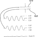
Among Figure 10,1001: drive the district, 1003: sensing area, 1007:TFT, 1009:TFT, 1011: gate line, 1012: gate line, 1013: data line, 1014: data line, the 1015:xVcom line, 1016:yVcom line, 1017:yVcom line part, 1019: pixel electrode, 1021: pixel electrode, 1023: common electrode Vcom, 1025: common electrode Vcom, 1026: charge amplifier.
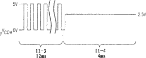
Among Figure 11 A-B, 11-1:LCD, 11-2: touch (VSTIM) 11-3:LCD, 11-4: touch.
Among Figure 13 A-13B, 1301: driving-sensing access area, 1303: driving-driving access area, 1304: grid, 1305: in the plane/open circuit (Y-disconnections) 1308 in the layer: outside the plane/layer outer bypass (Z-bypass), 1309: in the plane/layer in open circuit (X-disconnections) 1310: the connection, 1311: multiplexer, 1313: ground, 1321: grid, 1325: the bypass conductive path, 13-1: drive 13-2: sensing, 13-3:xVcom, 13-4:yVcom, 13-5: sensing area, 13-6: drive wire.
Among Figure 14 A, Figure 15 A, Figure 16 A, Figure 14 B, Figure 15 B and Figure 16 B, 1403: gate line, 1405:xVcom, 1407:vVcom, 1409: data line, 1411:x-y-com connects, 1413: common electrode (Vcom), 1503: gate line, 1505:xVcom (driving tunnel), 1507: data line, 14-1: expansion xVcom, 14-2:CON1,14-3: polysilicon transistors (part), 14-4: polysilicon transistors (part), 14-5:COM2,14-6:CON 2.
Among Figure 14 C, Figure 15 C and Figure 16 C, 1509: connect grid, 1603: connect grid, 14-7: pixel electrode, the 14-8:M3 layer, 14-9:CON 3, the 15-1:M3 layer.
Among Figure 17,17-1:A pixel, 17-2:B_ pixel, 17-3:C_ pixel, 17-4:D_ pixel, 17-5:E_ pixel, 17-6:F_ pixel, 17-7:G_ pixel, 17-8:H_ pixel, 17-9: shelter sequence (polysilicon/grid/CON1/ data).
Among Figure 18,18-1:A_ pixel, 18-2:B_ pixel, 18-3:C_ pixel, 18-4:D_ pixel, 18-5:E_ pixel, 18-6:F_ pixel, 18-7:G_ pixel, 18-8:H_ pixel, 18-9: shelter sequence (data/CON2/ITOVCOM).
Among Figure 19,19-1:A_ pixel, 19-2:B_ pixel, the 19-3:C_ pixel, 19-4:D_ pixel, 19-5:E_ pixel, the 19-6:F_ pixel, the 19-7:G_ pixel, 19-8:H_ pixel, 19-9: shelter sequence (ITOVCOM/ the 3rd metal level/CON3), 19-10:X-connects, 19-11:X-disconnects, and 19-12:Y-connects, and 19-13:Y-disconnects.
Among Figure 20,20-1:A_ pixel, 20-2:B_ pixel, 20-3:C_ pixel, 20-4:D_ pixel, 20-5:E_ pixel, 20-6:F_ pixel, 20-7:G_ pixel, 20-8:H_ pixel, 20-9: shelter sequence (the 3rd metal level/CON3/ pixel ITO/BM).
Among Figure 21 A, 2101: touch-screen, 2103: touch pixel, 2105: drive the tunnel, 21-1: 64 * 64 display pixels of every touch pixel, 21-2:10 unit (C0 to C9), 21-3:15 unit (R0 to R14), and the 21-4:A_ pixel (x-con, y-con), 21-5:B_ pixel (+x-discon, y-con), the 21-6:C_ pixel (x-con ,-y-discon), 21-7:D_ pixel (+x-discon,-y-discon), and the 21-8:E_ pixel (+x-discon, y-con), 21-9:F_ pixel (x-con, y-con), and the 21-10:G_ pixel (+x-discon, y-con), the 21-11:H_ pixel (x-con, y-con)
Among Figure 22-1,221-1:LCD FPC, 221-2: touch FPC, 221-3: anterior outshot, 221-4: 64 pixels of every row, 221-5: gate drivers, 221-6:LCD drives, the 221-7:M2/M3 bilayer, 221-8: the 3rd metal, 221-9: metal 2,221-10: metal 1.
Among Figure 22-2,222-1: pin assignment, 222-2:TSW (data multiplexer), 222-3:Z data line, 222-4: the 3rd metal, 222-5:x and y data line.
Among Figure 23,2301: overlayer, 2302: adhesive coating, 2303: polarizer, 2304: high R screen layer, 2305:CF glass, 2309: drive district's part, 2313: sensing area, 2315: the access area, 2316:TFT glass, 2317: the second polarizers, 23-1: drive 23-2: sensing.
Embodiment
Cross reference to related application
The application advocates the U.S. Provisional Application No.61/149 of application on February 2nd, 2009, the U.S. Provisional Application No.61/156 of application on February 27th, 340 and 2009, and 463 right, the content of described application is incorporated herein with way of reference in full for all purposes.
In the following description to exemplary embodiment, referring to accompanying drawing, described accompanying drawing forms the part of this paper and shows the specific embodiment that can put into practice embodiment of the present utility model in the mode of explanation therein.Should be understood that under the situation of the scope that does not break away from embodiment of the present utility model, can use other embodiment and can make structural change.
Below describe and comprise that the touch-sensing circuit can be integrated into the example in the display display pixel lamination (that is, forming the stacked material layers of display pixel) of (such as, LCD display).Though describe herein embodiment with reference to LCD display, should be understood that to utilize to substitute display and replace LCD display, but such as the general any electric imageable layer that contains the electricity image forming material.But the electricity image forming material can be luminescent material or light modulating materials.Luminescent material can be inorganic or organic in essence.Suitable material can comprise organic light emitting diode (OLED) or polymerization light-emittingdiode (PLED).Light modulating materials can be reflection or transmission.Light modulating materials can be including but not limited to electrochemical material, electrophoresis material (such as, twist type (Gyricon) particle), electrochromic material or liquid crystal material.Liquid crystal material can be (being not limited to) twisted nematic (TN), STN Super TN (STN), ferroelectric, magnetic or to palm property to row (chiral nematic) liquid crystal.Other suitable materials can comprise thermochromic material, charged particle and magnetic particle.The touch-sensing circuit can comprise (for example) touch signal line (such as, drive wire and sense wire), access area and other circuit.The display pixel lamination is made by the technology that comprises the following usually: such as conductive material (for example, the conductor of metal, substantial transparent), semiconductive material (for example, polysilicon (Poly-Si)) and the deposition of the material of dielectric material (for example, SiO2, organic material, SiNx), shelter, etching, doping etc.Be formed at various structures in the display pixel lamination and can be designed circuit operation as display system on display, to produce image.In other words, some in the described rhythmo structure can be the circuit components of display circuit.Some embodiment of integrated touch screen can comprise the multifunction electric circuit component, described multifunction electric circuit component can form the part of the display circuit of display system, and also can form the part of the touch-sensing circuit of touch-sensing system, on this touch-sensing system sensor display or near one or more touches.Described multifunction electric circuit component can be the capacitor in the display pixel of (for example) LCD, it can be configured to as the holding capacitor/electrode of the display circuit in this display system, common electrode, lead/conductive path etc. and operate, and also can be configured to as the circuit component of this touch-sensing circuit and operate.For example, in this way, in certain embodiments, can use less part and/or treatment step manufacturing to have the display of integrated touch sensing function, and display self can be thinner, brighter and need less electric power.
Can describe exemplary embodiment with reference to cartesian coordinate system herein, wherein x direction and y direction can be equal to horizontal direction and vertical direction respectively.Yet, it will be understood by those skilled in the art that with reference to the preferred coordinate system only for purpose clearly, and be not that direction with described structure is limited to specific direction or preferred coordinate system.In addition, although in the description of exemplary embodiment, may comprise concrete material and material type, it will be appreciated by those skilled in the art that and to use the other materials of reaching identical function.For example, should be understood that as " metal level " described in the following example and can be any conductive material layer.
In some exemplary embodiments, the matrix that LCD display with integrated touch sensing function can comprise the voltage data line with during the demonstration stage to the multifunction electric circuit component addressing of display pixel with display image, and during the touch-sensing stage to the multifunction electric circuit component addressing of display with sensing touch.Therefore, in certain embodiments, described multifunction electric circuit component can be used as the part operation of display system during the demonstration stage, and can be used as the part operation of touch-sensing system during the touch-sensing stage.For example, in certain embodiments, available first drive signal of some during the touch-sensing stage in the described pressure-wire drives to drive the driving district of touch-screen.In addition, one or more available second drive signal in the described pressure-wire drives, and this second drive signal is asynchronous with respect to first drive signal in order to the driving district that drives touch-screen, phase phasic difference 180 degree.These asynchronous pressure-wires can be used for reducing the direct capacitance of touch-screen.
In the potential advantage of various embodiment of the present utility model some (such as, thin, brightness and electrical efficiency) can be particularly useful for portable set, although the purposes of embodiment of the present utility model is not limited to portable set.Figure 1A to Fig. 1 C shows the example system that can implement according to the integrated touch screen of embodiment of the present utility model.Figure 1A explanation comprises the exemplary mobile phone 136 of integrated touch screen 124.Figure 1B explanation comprises the exemplary digital media player 140 of integrated touch screen 126.Fig. 1 C explanation comprises the exemplary personal computer 144 of integrated touch screen 128.
Fig. 1 D to Fig. 1 G explanation is according to the exemplary integrated touch-screen system 150 of comprising of embodiment of the present utility model of exemplary integrated touch-screen 153.Referring to Fig. 1 D, touch-screen 153 comprises display pixel 155, and display pixel 155 comprises the multifunction electric circuit component.Fig. 1 D shows the enlarged drawing of a display pixel 155, it comprises multifunction electric circuit component 157,159 and 161, described multifunction electric circuit component can be used as the part operation by the display system of display system controller 170 controls, and can be used as the part operation of the touch-sensing circuit of the touch-sensing system of being controlled by touch-sensing system controller 180.Display pixel 155 also comprises multifunction electric circuit component 163, and its display circuit, this touch-sensing system that can be used as this display system reaches the part operation by the electric system of power system controller 190 controls.Display pixel 155 also comprises: single function display circuit element 165, its in certain embodiments can be only as the part operation of this display circuit; And single function touch-sensing circuit component 167, its in certain embodiments can be only as the part operation of this touch-sensing circuit.
The exemplary operation of Fig. 1 E to Fig. 1 G explanation touch-screen system 150 comprises the different operating stage.Fig. 1 E is illustrated in the exemplary operation during the demonstration stage, and wherein the circuit component of display pixel 155 can be operated with display image on touch-screen 153.Operation during this demonstration stage can comprise that (for example) makes touch-sensing circuit component 167 separate with the circuit component electricity of this display circuit by (for example) with switch 169a to 169e or disconnect display pixel 155 is configured to configurations shown on one's own initiative.The circuit component that disposes display pixel on one's own initiative can comprise with the part operation as the circuit of the particular system of integrated touch screen, for example, switch connection, unlatching/turn off circuit component between the line of different system, change pressure-wire voltage level, change signal (such as, control signal) or the like.Active arrangement can occur in touch-screen operating period and can be to the static configuration of small part based on this touch-screen, that is, and structural arrangements.Structural arrangements can comprise that size, shape, placement, the material of the structure in the lamination of (for example) display pixel form or the like, such as the number of the conductive path in the display pixel lamination and placement, the permanent connection (such as, the conductor filled through hole that connects the contact point of two conductive layers), forever open circuit (such as, the part that in design, has removed conductive material of conductive path) or the like.
Fig. 1 F is illustrated in the exemplary operation during the touch-sensing stage, and wherein the circuit component of display pixel 155 can be operated to make touch-sensing circuit component 167 and switch 169b and 169c be electrically connected and make display system circuit component 165 and switch 169a and 169d electricity to disconnect sensing touch (comprise and dispose display pixel on one's own initiative to be used for touch-sensing) by (for example).But touch-sensing system controller 180 transmission of control signals 181 and accessible information signal 183 and 185.In certain embodiments, control signal 181 can be the drive signal that (for example) be used for capacitance sensing, the drive signal that is used for the optics sensing or the like.In certain embodiments, information signal 183 can be the sensing signal that (for example) is used for capacitance sensing, optics sensing or the like, and information signal 185 can be the feedback signal of (for example) this touch-sensing system.
Fig. 1 G is illustrated in the exemplary operation during the electric system stage, and wherein the multifunction electric circuit component 163 of display pixel 155 can disconnect with this display system and this touch-sensing system electricity by switch 169c, 169d and 169e.Power system controller 190 can be come transmission signals 192 via multifunction electric circuit component 163.Signal 192 can be the signal that (for example) indicates the state that recharges of this electric system, supply voltage or the like.
In embodiment more of the present utility model, this touch-sensing system can be based on electric capacity.By the change that detects each electric capacity that touches the pixel place and mark described touch locations of pixels, but a plurality of objects of this touch-sensing system identification, and when described object is mobile on touch-screen, judge position, pressure, direction, speed and/or the acceleration of described object.
For example, some embodiment of integrated touch sensing system can be based on self-capacitance, and some embodiment can be based on mutual capacitance.In the touch system based on self-capacitance, each touches pixel and can be formed by the individual electrode that forms self-capacitance over the ground.When an object touched pixel near this, another ground capacitance (capacitance to ground) can be formed between this object and this touch pixel.The net increase of the self-capacitance that this touch pixel that can cause this another ground capacitance is stood.This self-capacitance increase can detect and measure to judge the position of a plurality of objects when touching this touch-screen by this touch-sensing system.In the touch system based on mutual capacitance, this touch-sensing system can comprise that (for example) drives district and sensing area, such as drive wire and sense wire.In an example case, drive wire can form multirow, and sense wire can form multiple row (for example, quadrature).Described touch pixel can be arranged at row and locate with the point of crossing of row.During operation, available AC waveform encourages described row, and mutual capacitance can be formed between the row and row of this touch pixel.When an object touches pixel near this, be coupled in the row of this touchs pixel and be listed as between some electric charges can change into and being coupled on this object.The clean minimizing of the mutual capacitance between this minimizing that is coupled in the electric charge on this touch pixel can cause row and be listed as and be coupled in the minimizing of the AC waveform on this touch pixel.This minimizing of electric charge coupling AC waveform can detect and measure to judge the position of a plurality of objects when touching this touch-screen by this touch-sensing system.In certain embodiments, integrated touch screen can be multiple point touching, single-point touches, projection scanning, full imaging multiple point touching, or any capacitance touch.
Fig. 2 is the block diagram of an exemplary computer system 200, and its explanation is according to a kind of enforcement of the exemplary integrated touch-screen 220 of embodiment of the present utility model.Computing system 200 can be included in (for example) mobile phone 136, digital media player 140, personal computer 144, or comprises in any mobile or non-moving computing equipment of touch-screen.Computing system 200 can comprise touch-sensing system, and it comprises one or more touch processor 202, peripheral equipment 204, touch controller 206 and touch-sensing circuit (describing in more detail hereinafter).Peripheral equipment 204 can include, but is not limited to the internal memory of random-access memory (ram) or other types or storer, watchdog timer (watchdog timer), or the like.Touch controller 206 can include, but is not limited to one or more sense channel 208, channel scan logic 210 and driver logic 214.But channel scan logic 210 access RAM 212, independently read and control to described sense channel is provided from the data of described sense channel.In addition, as described in greater detail below, channel scan logic 210 controllable driver logics 214 are in the pumping signal 216 of various frequencies and phase place with generation, and described pumping signal 216 optionally puts on the driving district (as more detailed description hereinafter) of the touch-sensing circuit of touch-screen 220.In certain embodiments, touch controller 206, touch processor 202 and peripheral equipment 204 can be integrated in the single asic (ASIC).
Computing system 200 can comprise that also host-processor 228 carries out action to be used to receive from the output of touch processor 202 and based on described output.For example, host-processor 228 can be connected to program storage 232 and display controller, such as lcd driver 234.Host-processor 228 can use lcd driver 234 to produce image on touch-screen 220, image such as user interface (UI), and can use touch processor 202 and touch controller 206 to come on the senses touch screen 220 or near touch, such as touch input to shown UI.This touch input can be by being stored in computer program in the program storage 232 in order to carry out following action, described action can include, but is not limited to move the object such as vernier or index, scrolling or translation (panning), adjusting control sets, open file or document, check menu, select, execution command, be operatively connected peripheral equipment to main process equipment, answer the call, make a phone call, hang up, change volume or audio settings, storage is such as the address, often dial the number, incoming call, the information relevant of missed call with telephone communication, log into thr computer or computer network, allowance is through the confined area of authorized individuals access computing machine or computer network, be written into the computer desktop of user preference and arrange the user profiles that is associated, permit access network (web) content, the beginning specific program, encrypt or decode messages, and/or similar action.Host-processor 228 also can be carried out may not relevant with touching processing additional functionality.
Touch-screen 220 can comprise the touch-sensing circuit, and it can comprise the capacitance sensing medium with a plurality of drive wires 222 and a plurality of sense wire 223.Should note, understandable as those skilled in the art institute, term " line " only means conductive path sometimes when using in this article, and is not limited to strict linear structure, but comprise the path that changes direction, and comprise the path of different sizes, shape, material or the like.Drive wire 222 can be by driving via the pumping signal 216 of driving interface 224 from driver logic 214, and the gained sensing signal 217 that produces in sense wire 223 can transfer to sense channel 208 (also being called event detection and demodulator circuit) in the touch controller 206 via sensing interface 225.In this way, drive wire and sense wire can be the parts of this touch-sensing circuit, and described drive wire and sense wire can interact to form the capacitance sensing node, and described node can be taken as and touch element (touch pixel), such as touching pixel 226 and 227.When touch-screen 220 was regarded as catching " image " of touch, this understanding mode can be particularly useful.In other words, after touch controller 206 has judged whether the touch of each in this touch-screen pixel place detects touch, the pattern that the touch pixel of touch takes place in the touch-screen can be taken as " image " (for example, pattern of this touch-screen of finger touch) of touch.
Fig. 3 is the more detailed view of touch-screen 220, and it shows the exemplary configuration according to drive wire 222 and the sense wire 223 of embodiment of the present utility model.Such as among Fig. 3 displaying, each drive wire 222 can be formed by one or more drive wire sections 301, described section can be electrically connected by drive wire link 303 connecting 305 places.Drive wire link 303 is not electrically connected to sense wire 223, and on the contrary, the drive wire link can be walked around sense wire via bypass 307.But drive wire 222 interacts with sense wire 223 condenser types and touches pixel to form, such as touching pixel 226 and 227.Drive wire 222 (that is, drive wire section 301 and respective drive wired link 303) and sense wire 223 can be formed by the circuit component in the touch-screen 220.In the exemplary configuration of Fig. 3, each that touches in the pixel 226 and 227 can comprise the part of a drive wire section 301, the part of a sense wire 223 and the part of another drive wire section 301.For example, touch the right half part 309 of the drive wire section on the side of a part 311 that pixel 226 can be included in a sense wire, and the left-half 313 of the drive wire section on the opposite side of the part 311 of this sense wire.
As described above, described circuit component can comprise that (for example) can be present in the structure in traditional LCD display.Note that circuit component is not limited to the entire circuit assembly, such as whole capacitor device, whole transistor or the like, but can comprise the part of circuit, such as only one in two plates of plane-parallel capacitor.Fig. 4 illustrates an exemplary configuration, and wherein common electrode (Vcom) can form the part according to the touch-sensing circuit of the touch-sensing system of embodiment of the present utility model.Common electrode be some type traditional LCD display (for example, the lamination of display pixel fringing field switching (FFS) display) (promptly, the circuit component of the display system circuit the stacked material layers of formation display pixel), its part operation that can be used as display system is with display image.In the example of in Fig. 4, being showed, common electrode (Vcom) 401 (for example, the element 161 of Fig. 1 D) can serve as the multifunction electric circuit component, this multifunction electric circuit component can be used as the display circuit operation of the display system of touch-screen 220, and also can be used as the touch-sensing circuit operation of this touch-sensing system.In this example, common electrode 401 can be used as the common electrode operation of the display circuit of this touch-screen, and also can be with the touch-sensing circuit operation of other common electrodes as this touch-screen after grouping.For example, the group of common electrode 401 can operate as the drive wire of this touch-sensing circuit or the capacitive part of sense wire during the touch-sensing stage together.Common electrode 401 by (for example) Jiang Yi district is electrically connected, switches electrical connection or the like, and other circuit components of touch-screen 220 can form the part of touch-sensing circuit.Generally speaking, each in the described touch-sensing circuit component can be: the multifunction electric circuit component, and it can form the part of this touch-sensing circuit and can carry out one or more other functions, such as the part that forms display circuit; Or can be the unifunctional circuit element, it only can be used as the touch-sensing circuit operation.Similarly, each in the display circuit element can be: the multifunction electric circuit component, and it can be used as display circuit operation and carries out one or more other functions, such as the touch-sensing circuit operation; Or can be the unifunctional circuit element, it only can be used as the display circuit operation.Therefore, in certain embodiments, some in the circuit component in the display pixel lamination can be the multifunction electric circuit component, and other circuit components can be the unifunctional circuit element.In other embodiments, all circuit components of display pixel lamination can be the unifunctional circuit element.
In addition, although exemplary embodiment herein may be described as display circuit showing the stage manipulate, and the touch-sensing circuit is described as in touch-sensing stage manipulate, but should understand, demonstration stage and touch-sensing stage can operate simultaneously, for example, partially or completely overlapping, or demonstration stage and touch stage can operate at different time.Although exemplary embodiment herein is described as some circuit component multi-functional and other circuit components is described as unifunctional, should be understood that circuit component is not limited to particular functionality in other embodiments again.In other words, the circuit component that is described to the unifunctional circuit element in the exemplary embodiment in this article can be configured to the multifunction electric circuit component in other embodiments, and vice versa.
For example, Fig. 4 shows and to be grouped into together the common electrode 401 that drives trivial section 403 and sensing area 405 to form that described section corresponds respectively to drive wire section 301 and sense wire 223 substantially.The grouping of the multifunction electric circuit component of display pixel can be meaned that the multifunction electric circuit component that makes described display pixel operates together to carry out the common function in this district to the district.Being grouped into functional areas can make up via a kind of method or method and finish, for example, operative configuration of the structural arrangements of system (for example, entity opens circuit and the configuration of bypass, pressure-wire), system (for example, voltage level and/or the signal on connections/cut-out circuit component, the change pressure-wire) or the like.
In certain embodiments, the grouping of circuit component can be embodied as the layout of display pixel, and each display pixel is the set that is selected from a finite population display pixel configuration.In certain embodiments, a specific function of touch-sensing circuit can be provided by the display pixel of the particular type with the configuration that can carry out this function.For example, hereinafter can comprise referring to the described embodiment of Figure 17 to Figure 22: the display pixel of the type that the one or more neighbors in the articulamentum of lamination can be linked together, can provide to the display pixel of the type of the contact of another layer of lamination, and the display pixel of the type that the one or more neighbors in another layer can be linked together.
In certain embodiments, the district can be reconfigurable (for example) to allow group pixels to the district of different sizes, difformity or the like.For example, some embodiment can comprise that switching array able to programme (depends on the display pixel grouping to allow reconfigurable handover scheme to the district of different sizes, for example, the variation of environmental noise, treat sensing article the size and/or its distance apart from touch-screen, or the like).Can allow other aspects of the configuration of dividing into groups may be not for reconfigurable, for example, it not be reconfigurable that the entity in the line in the lamination of display pixel opens circuit.Yet, by comprise reconfigurable other circuit components (such as, programmable switch, signal generator or the like), comprise that the touch-screen configuration that (for example) entity opens circuit still can allow display pixel is divided into groups to the district of different sizes, difformity or the like reconfigurablely.
The multifunction electric circuit component of the display pixel of touch-screen can be operated in demonstration stage and touch stage.For example, during the touch stage, common electrode 401 can be grouped into together to form the touch signal line, such as driving district and sensing area.In certain embodiments, circuit component can be through grouping to form one type the continuous touch signal line and the sectional type touch signal line of another kind of type.For example, Fig. 4 shows an exemplary embodiment, wherein drives trivial section 403 and sensing area 405 drive wire section 301 and the sense wire 223 corresponding to touch-screen 220.In other embodiments, other are configured to possible, and for example, common electrode 401 can be grouped into together, so that each free continuous drive district of drive wire forms, and each freedom of sense wire forms via walking around the connection link a plurality of sensing area sections together that drive the district.The more details of the operation in exemplary demonstration stage and exemplary touch stage are described referring to Figure 11 A to Figure 11 B hereinafter.
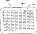
Driving district in the example of Fig. 3 is shown as the rectangle region of a plurality of common electrodes that comprise display pixel in Fig. 4, and the sensing area of Fig. 3 is shown as the rectangle region of a plurality of common electrodes that comprise display pixel that extend in the vertical length of LCD in Fig. 4.In certain embodiments, the touch pixel of the configuration of Fig. 4 can comprise the zone of (for example) 64 * 64 display pixels.Yet, drive district and sensing area and be not limited to shape, orientation and the position showed, but can comprise any suitable configurations according to embodiment of the present utility model.Should be understood that being used to form the display pixel that touches pixel is not limited to above-mentioned display pixel, but can be any suitable size or the shape of the ability that touches according to the allowance of embodiment of the present utility model.
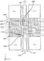
Fig. 5 explanation is according to the exemplary configuration of the conductor wire of embodiment of the present utility model, in the district that described conductor wire can be used for common electrode 401 is divided into groups to Fig. 4 to be showed and link drive trivial section to form drive wire.Illustrated in the exemplary embodiment as show in Figure 13, some embodiment can comprise other districts, such as between the drive wire and/or the access area between drive wire and sense wire.
Fig. 5 shows a plurality of yVcom lines 503 that reach along the y direction along a plurality of xVcom lines 501 of x direction.In this embodiment, each row common electrode 401 can have corresponding xVcom line 501, and each row common electrode 401 can have corresponding yVcom line 503.Fig. 5 further shows trivial section 403 of a plurality of driving (by the dotted line explanation), wherein each drives trivial section 403 group that can form the common electrode 401 that links together via x-y-com connection 505, as described in greater detail below, described x-y-com connects 505 each common electrode is connected to xVcom line 501 and yVcom line 503 in driving trivial section.Extend through the yVcom line 503 that drives trivial section 403 (such as, yVcom line 503a) and can comprise that providing each to drive trivial section opens circuit 509 with other electricity that drive trivial section (for example, the section of trivial section top of given driving and below) separate.Opening circuit 509 can provide y to disconnect (electricity on the y direction disconnects).
But drive wire 511 each free a plurality of driving form for trivial section 403, and these a plurality of drivings can be formed by common electrode 401 and interconnecting electroconductive wires by means xVcom thereof for trivial section 403.Particularly, can form drive wire 511 for trivial section 403 by using xVcom line 501 to stride across sensing area 405 connection drivings.Such as among Fig. 5 displaying, the first drive wire 511a can be formed for trivial section 403 by the driving of top row, and next drive wire 511b can drive trivial section 403 by next line and forms.As described in greater detail below, the xVcom line is walked around the conductive path of the yVcom line in the sensing area 405 for using bypass 513.
Fig. 5 further shows a plurality of sensing areas 405 (by the dotted line explanation).Each sensing area 405 can form the group that connects 507 common electrodes that link together 401 via y-com, and described y-com connects 507 one of each common electrode of sensing area 405 can be connected in the yVcom line 503.Extra connect (seeing (for example) Figure 10) can link together the yVcom line of each sensing area 405.For example, described extra connection can be included in the switch in the border of touch-screen 220, and it can be during the touch stage of operation links together the yVcom line of each sensing area.The yVcom line 503 (such as, yVcom line 503b) that extends through sensing area 405 can be electrically connected all common electrodes 401 on the y direction, so the yVcom line of sensing area does not comprise and opening circuit.In this way, for example, one sensing area can be formed by a plurality of vertical common voltage line yVcom that is connected to each other and be connected to the circuit component of respective display pixel, forms the sense wire of being made up of the circuit component of the electrical connection of the display pixel in the sensing area 512 by this.In the exemplary sensing area of being showed in Fig. 5, vertical common voltage line yVcom can (at 513 places) be connected with horizontal common voltage line xVcom and can crosses horizontal common voltage line xVcom to be formed for the structure of capacitance touch sensing.This crosses yVcom and xVcom also can and drive formation additional parasitic electric capacity between the district at sensing area.
Each common electrode 401 can be corresponding to the display pixel of touch-screen 220, such as display pixel 515 and 517.During the demonstration stage, common electrode 401 is operated with display image on touch-screen as the display circuit of the display system of touch-screen 220 together with other display pixel assemblies.During the touch stage, the group of common electrode 401 can be used as the touch-sensing circuit operation of the touch-sensing system of touch-screen 220 and goes up or near one or more touches with the senses touch screen.
In the operation during the touch stage, horizontal common voltage line xVcom 501 can transmit pumping signal and form electric field with excitation drive wire 511 and between excited target drive wire and sense wire 512 to produce the touch pixel, such as the touch pixel 226 among Fig. 3.Such as the object of finger near or touch when touching pixel, this object can influence the electric field that extends between drive wire 511 and sense wire 512, minimizing is capacitively coupled to the quantity of electric charge of sense wire by this.This electric charge reduces and can be sensed by sense channel, and is stored in the storer to produce " image " that touches together with other similar information that touch pixel.
In certain embodiments, drive wire and/or sense wire can be formed by other structures, comprise (for example) be present in the typical LCD display other structures (for example, other electrodes, conduction and/or semi-conductive layer, metal wire, circuit component in its LCD display that also will serve as a model, for example, the carrying signal, storage voltage or the like), and atypia LCD rhythmo structure be formed in the LCD lamination other structures (for example, other metal wires, plate, its function will be used for the touch-sensing system of touch-screen substantially) and be formed at the outer structure of LCD lamination (for example, such as the current-carrying plate of outside substantially transparent, line and other structures).For example, the part of touch-sensing system can comprise the structure that is similar to known touch panel superstratum.Partially or completely use the structure that has been present in the display to form touch-sensing system and can increase the image quality of touch-screen, brightness or the like potentially by reducing the amount of covering the structure that mainly is exclusively used in touch-sensing of display in the common meeting.
In certain embodiments, for example, display pixel can divide into groups to one drive between district and the sensing area and/or two districts that drive between distinguishing in, and these districts can be connected to ground connection or virtual ground forming the access area, drive between the district and/or drive interference between district and the sensing area so that further minimize.Figure 13 A to Figure 13 B shows the exemplary layout according to the district of embodiment of the present utility model, and it is included in and drives between the district and the access area between driving district and sensing area.In other embodiments, can save vertical common voltage line and open circuit, and described line is driving the interval by intactly shared.
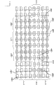
In Fig. 5, display pixel 515 can divide into groups to sensing area 405, and display pixel 517 can divide into groups to driving in trivial section 403.Fig. 6 to Fig. 8 illustrates the display pixel 515 in the exploded view 5 " square frame A " and the planimetric map and the side view of 517 more details, and show according to exemplary opening circuit/bypass in the comprising in the plane of embodiment of the present utility model/layer and plane outer/exemplary configuration of layer exemplary opening circuit/bypass outward.
Fig. 6 is the enlarged drawing of " square frame A " among Fig. 5, and it shows the more details of display pixel 515 and 517 and according to other structures of the touch-screen 220 of embodiment of the present utility model.Display pixel 515 and 517 can comprise community electrode 401 and three display pixel electrodes 601 separately, described display pixel electrode is used for redness (R) sub-pixel, green (G) sub-pixel and blueness (B) sub-pixel corresponding to R data line 603, G data line 605 and B data line 607 separately, when connecting the transistor 609 of described sub-pixel by being applied to the voltage on the gate line 611 during the demonstration stage at touch-screen, described data line offers described sub-pixel with color data.
In certain embodiments, can use the display pixel of other types, such as monochromatic (for example, black and white) display pixel, comprise display pixel greater or less than three sub-pixels, invisible spectrum (such as, infrared ray) display pixel of operation in, or the like.Different embodiment can comprise the display pixel with different sizes, shape, optical property.The display pixel of some embodiment relative to each other can have different sizes, shape, optical property or the like, and in certain embodiments, the dissimilar different functionalities that provide of the display pixel that is utilized in the touch-screen.
Fig. 6 also illustrates that the yVcom line 503 that extends through display pixel 517 has makes display pixel 517 (and the driving of display pixel 517 trivial section 403, see Fig. 5) open circuit 509 with trivial section of adjacent driven is separated.509 the examples that open circuit for opening circuit in the plane, it is the open circuit of the electricity between the conductive path that extends substantially (electrical open) in same plane, this plane is the x-y plane that yVcom line 503 extends therein in such cases.Equally, such as hereinafter description, opening circuit 509 is the example that opens circuit in the layer, it is the open circuit of the electricity between the conductive path that extends in one deck, be second metal level at this layer in such cases.Though opening circuit in many layers also may be for opening circuit in the plane, situation must be not like this.For example, opening circuit in the conductive path of the material layer in the lamination can appear at this layer and be formed at different stack height (promptly, Different Plane) position of locating, and therefore in opening circuit of this position will be for layer, open circuit outside the plane, but not in the layer, open circuit in the plane.
On the other hand, the yVcom line 503 that extends through the display pixel 515 of sensing area 405 does not comprise and opening circuit, make display pixel 515 can be electrically connected to other display pixels of sensing area 405 on the y direction, that is, the display pixel in this sensing area is (y-connected) that y connects.
XVcom line 501 extends through display pixel 515 and 517 on the x direction.Such as in the enlarged drawing at the xVcom of R data line 603 back of display pixel 515 left upper displaying, xVcom line 501 is located at other R data line 603 of branch, G data line 605 and B data line 607 back.Being connected in the exploded view that is showed in more detail among Fig. 6 between display pixel 515 and 517 xVcom line and yVcom line and the common electrode 401, it also shows that xVcom line 501 is located at yVcom line 503 back, and yVcom line 503 is located at common electrode 401 back.For the display pixel 515 of sensing area, the y-com of display pixel 515 connects 507 shown in exploded view y-com and (for example is connected to the yVcom line 503 of this display pixel and the conductor wire 613 between the electrode 401 jointly, be filled with the through hole of conductive material), and showed between xVcom line 501 and yVcom line 503, not have and be connected, promptly, bypass 513 (and therefore, do not have between xVcom line and this common electrode be connected).Because bypass 513, display pixel 515 can be the x disconnection, or isolate on the x direction, that is, and along x direction and adjacent display pixels disconnection or isolation.In this exemplary embodiment, the extra connection of the yVcom line 503 of sensing area (such as, above-mentioned boundary switch) common electrode 401 of display pixel 515 is electrically connected to common electrode at the adjacent sensing area display pixel on display pixel 515 left sides, therefore bypass 513 make display pixel 515 with at the adjacent driven district on display pixel 515 the right display pixel 517 " the right disconnection " (in other words, display pixel 515 can disconnect with display pixel x on positive x direction, that is, positive x disconnects).
For the display pixel 517 of trivial section of driving, the x-y-com of display pixel 517 connects this x-y-com of shown in exploded view of 505 and connects and can comprise the conductor wire 615 that the xVcom line is connected to the yVcom line, and the yVcom line is connected in the conductor wire 613 of common electrode one.Therefore, the common electrode of each display pixel in driving trivial section can be electrically connected, and this is because each display pixel can be connected to the same conductive grid of perpendicular line (yVcom) (that is, y connects) and horizontal line (xVcom) (that is, x-connects).In this exemplary configuration, common electrode, perpendicular line and horizontal line are can be in different cardinal principle coplanar flat directed and connect and link together via two groups, and one group connects perpendicular line and horizontal line, and another group connects perpendicular line and common electrode.This configuration (comprising opening circuit in the perpendicular line) is for being grouped into the circuit component of display together the example with the touch-sensing circuit that forms a drive wire in driving trivial section, this drive wire can chain to other drive wire sections via the drive wire link of the sense wire of walking around intervention.
Fig. 7 to Fig. 8 is respectively the cross-sectional view of the part of the part of explanation display pixel 515 laminations and display pixel 517 laminations.Fig. 7 shows along the view from the xsect of the display pixel 515 of the line intercepting that arrow is arranged of the 7-7 ' of Fig. 6.Fig. 7 comprises the gate line 611 and the xVcom line 501 that are formed in the first metal layer (M1), is formed at B data line 607, drain electrode 701 and yVcom line 503 in second metal level (M2).This figure also comprise by transparent conductor (such as, ITO) common electrode 401 of Xing Chenging and display pixel electrode 601.Common electrode 401 can be electrically connected to yVcom line 503 via the through hole among the dielectric layer 707a (conductive through hole 703, it is an example of the conductor wire 613 of Fig. 6), and this through hole can be filled with conductive material.Fig. 7 also shows the bypass 513 (do not have and be connected) between xVcom 501 and the yVcom 503.Thus, bypass 513 can be taken as and make xVcom 501 and yVcom 503 separated structures, and it can comprise the part of dielectric layer 707b.Gate insulator 705 can comprise dielectric material, such as SiO2, SiNx or the like.It then is colored filter that liquid crystal layer can be placed in the pixel electrode top, and polarizer can be positioned on the top and bottom of lamination (not shown).About Fig. 7, touch-screen is watched from the top.
Fig. 8 shows along the view from the xsect of the display pixel 517 of the line intercepting that arrow is arranged of the 8-8 ' of Fig. 6.The bypass 513 that conductive through hole 801 in Fig. 8 is replaced among Fig. 7, Fig. 8 is identical with Fig. 7.Therefore, in driving trivial section display pixel 517, xVcom 501 can be electrically connected to yVcom 503.Therefore, the conductor wire among Fig. 6 615 through hole that is filled with conductor in the exemplary stack for this reason.
In a word, Fig. 7 to Fig. 8 explanation plane according to embodiment of the present utility model outer/layer is outer to open circuit/how the use of bypass can provide an example of the effective ways of the multi-functional touch-sensing LCD structure that generation comprises the multifunction electric circuit component in certain embodiments.In such cases, in certain embodiments, connection/bypass of making between the conductive path in Different Plane/layer can allow the more multiselect item of the design of multi-functional configuration, and can reduce potentially should need to add with in same plane/layer, form bypass added the number of structure (for example, line).Thus, in certain embodiments, can only in the Different Plane/layer of display pixel lamination, form conductive path by (for example) and form y disconnection and/or x disconnection expediently.Equally, in certain embodiments, the conductive path that can use the conductive path between Different Plane/layer to connect in Different Plane/layer forms y connection and/or x connection expediently.Especially, it is functional to add integrated touch according to embodiment of the present utility model that this can allow more easily to revise existing LCD design.Thus, to in the plane/layer in and the plane outer/layer is outer to open circuit and the selectivity of bypass uses more structures that can allow in the existing LCD design to be used as circuit component in the touch-sensing system, and can reduce existing manufacture process (such as, shelter, mix, deposit or the like) number of required change.
The more details of the illustrative methods of example touch screen and operating multifunction touch-screen LCD circuit component will be described referring to Fig. 9 to Figure 12 B.Fig. 9 is the partial circuit figure according to the example touch screen that comprises a plurality of sub-pixels 900 of embodiment of the present utility model.As in above-mentioned exemplary embodiment, the sub-pixel of touch-screen 900 can be configured, so that it can have the multifunctionality as LCD sub-pixel and touch sensor circuit component.That is, sub-pixel can comprise the part operation of the LCD circuit that can be used as display pixel and also can be used as the circuit component of the circuit component operation of touch-sensing circuit.In this way, touch-screen 900 can be used as the LCD operation with integrated touch sensing function.Fig. 9 shows the sub-pixel 901,902 of touch- screen 900 and 903 details.In this exemplary embodiment, each sub-pixel can be redness (R), green (G) or blue (B) sub-pixel, and wherein all three R, G and B sub-pixel is combined to form a color display pixel.Although this exemplary embodiment comprises redness, green and blue subpixels, sub-pixel can or can dispose based on monochrome based on the electromagnetic radiation (for example, infrared ray) of light or other wavelength of other colors.
Sub-pixel 902 can comprise have grid 955a, source electrode 955b and the drain electrode 955c thin film transistor (TFT) (TFT) 955.Sub-pixel 902 also can comprise community electrode (Vcom) 957b, and it can be (for example) at 901,902 and 903 shared continuous slabs of the material of conduction substantially of sub-pixel, such as the common electrode of being showed among Fig. 6 401.Sub-pixel 902 also can comprise can be with the pixel electrode 957a of common electrode 957b as the part operation of display system circuit.Pixel electrode 957a can (for example) pixel electrode 601 for being showed among Fig. 6 to Fig. 8.Touch-screen 900 can be used as the operation of FFS display system, and wherein the pixel electrode of each sub-pixel and common electrode produce the fringing field of the liquid crystal that is applied to this sub-pixel, and also can form the holding capacitor of this sub-pixel.Sub-pixel 902 can comprise the holding capacitor 957 that is formed by pixel electrode 957a and common electrode 957b.Sub-pixel 902 also can comprise a part of 917a of the data line (G data line 917) that is used for green (G) color data, and a part of 913b of a gate line 913.Grid 955a can be connected to gate line part 913b, and source electrode 955b is connected to G data line part 917a.Pixel electrode 957a can be connected to the drain electrode 955c of TFT 955.
Sub-pixel 901 can comprise have grid 905a, source electrode 905b and the drain electrode 905c thin film transistor (TFT) (TFT) 905.Sub-pixel 901 also can comprise a pixel electrode 907a, and this pixel electrode can be operated with generation with common electrode 957b and be used for the fringing field of this sub-pixel and form holding capacitor 907.Sub-pixel 901 also can comprise a part of 915a of the data line (R data line 915) that is used for redness (R) color data, and a part of 913a of gate line 913.Grid 905a can be connected to gate line part 913a, and source electrode 905b can be connected to R data line part 915a.Pixel electrode 907a can be connected to the drain electrode 905c of TFT 905.Sub-pixel 901 and 902 can comprise most or all structures of (for example) traditional LC D sub-pixel.
Sub-pixel 903 can comprise have grid 975a, source electrode 975b and the drain electrode 975c thin film transistor (TFT) (TFT) 975.Sub-pixel 903 also can comprise a pixel electrode 977a, and this pixel electrode can be operated with generation with common electrode 957b and be used for the fringing field of this sub-pixel and form holding capacitor 977.Sub-pixel 903 also can comprise a part of 919a of the data line (B data line 919) that is used for blueness (B) color data, and a part of 913c of gate line 913.Grid 975a can be connected to gate line part 913c, and source electrode 975b can be connected to B data line part 919a.Pixel electrode 977a can be connected to the drain electrode 975c of TFT 975.Be different from sub-pixel 901 and 902, sub-pixel 903 also can be included in a part of 925a of the upwardly extending common voltage line in y side (yVcom 925), and a tie point 929.In other embodiments, this yVcom is extensible by red sub-pixel or green sub-pixels, but not blue subpixels.One connection (such as, above connecting 505 referring to described y-com connection 507 of Fig. 6 or x-y-com) can carry out at tie point 929 places, so that (for example) is connected to common electrode 957b yVcom 925 (it vertically extends through other display pixels), common electrode 957b is connected to yVcom 925 and xVcom 921 (its horizontal-extending is by other pixels) or the like.For example, in this way, common electrode 957b can be connected to produce the district of connected common electrode with the common electrode of other display pixels.
Described in some exemplary embodiment, a kind of method that produces the Disengagement zone is for forming open circuit (open circuit) in level and/or vertical common line as mentioned.For example, yVcom 925 can have optional as show in Figure 9 opening circuit, and it can allow the sub-pixel of this top of opening circuit and the sub-pixel of this below of opening circuit to isolate, that is, described sub-pixel can disconnect the bottom.Can be by forming at tie point 929 places that y-com connects but not x-y-com connect and produce x-and disconnect, xVcom921 and common electrode 957b are disconnected.In certain embodiments, xVcom 921 can comprise and opening circuit that it can allow the sub-pixel on this right of opening circuit and the sub-pixel on this left side of opening circuit to isolate.Other configurations can allow the display pixel circuits element to divide into groups by the bypass link drive wire section together via sense wire as described above.
In this way, the common electrode of touch-screen 900 can be grouped into together to form a structure in display pixel, and this structure can be used as the part operation of the touch-sensing circuit of touch-sensing system.For example, described common electrode can be configured to form and drive district or sensing area, forms bypass and link as describing about some embodiment as mentioned, or the like.Thus, circuit component (such as, common electrode, xVcom line, or the like) can be used as the multifunctional circuit element operation.
Generally speaking, touch-screen 900 can be configured, so that the common electrode of all sub-pixels in this screen can (for example) linked together via at least one vertical common voltage line that has to the connection of a plurality of horizontal common voltage lines.Another touch-screen can be configured, so that different subpixel group can be joined together to form a plurality of Disengagement zone of the common electrode that links together.
To describe according to the touch-sensing of embodiment of the present utility model referring to Figure 10 to Figure 12 B and operate.Figure 10 shows according to the driving district 1001 of the example touch screen of embodiment of the present utility model and the partial circuit figure of some the touch-sensing circuit in the display pixel in the sensing area 1003.For clarity sake, Figure 10 comprises with the circuit component of dotted line explanation to represent that some circuit component is mainly as display circuit but not the part operation of touch-sensing circuit.In addition, mainly the touch-sensing operation is described according to single driving display pixel 1001a (for example, driving the single display pixel in district 1001) and single sensing display pixel 1003a (for example, the single display pixel of sensing area 1003).Yet, should understand, drive in the district 1001 other and drive display pixels and can comprise with hereinafter at driving the identical touch-sensing circuit of touch-sensing circuit that display pixel 1001a describes, and other sensing display pixels in the sensing area 1003 can comprise and hereinafter at the identical touch-sensing circuit of touch-sensing circuit of sensing display pixel 1003a description.Therefore, can be considered as description respectively to the description of the operation that drives display pixel 1001a and sensing display pixel 1003a to the operation that drives district 1001 and sensing area 1003.
Referring to Figure 10, drive district 1001 and comprise a plurality of driving display pixels, comprise driving display pixel 1001a.Drive display pixel 1001a and comprise TFT 1007, gate line 1011, data line 1013, xVcom line part 1015 and yVcom line part 1017, pixel electrode 1019, and common electrode 1023.Figure 10 shows common electrode 1023, and it is connected to via xVcom line part 1015 and yVcom line part 1017 and drives in the district 1001 other and drive common electrode in display pixels to be formed for the structure (as described in greater detail below) of touch-sensing in the display pixel that drives district 1001.Sensing area 1003 comprises a plurality of sensing display pixels, comprises sensing display pixel 1003a.Sensing display pixel 1003a comprises TFT 1009, gate line 1012, data line 1014, yVcom line part 1016, pixel electrode 1021, and common electrode 1025.Figure 10 shows common electrode 1025, and it is connected to common electrode in other sensing display pixels in the sensing area 1003 to be formed for the structure (as described in greater detail below) of touch-sensing in the display pixel of sensing area 1003 via the yVcom line part 1016 that can (for example) connects in the frontier district of touch-screen.
During the touch-sensing stage, the drive signal that puts on xVcom line part 1015 produces electric field between the structure through being connected common electrode 1025 of the structure through connecting common electrode 1023 that drives district 1001 and sensing area 1003, this structure of common electrode 1025 is connected to sensing amplifier, such as charge amplifier 1026.Electric charge is injected in the structure through connecting common electrode of sensing area 1003, and charge amplifier 1026 converts the electric charge injection to measurable voltage.The quantity of electric charge that is injected and therefore measured voltage can be depending on and touch the object (such as, finger 1027) and the degree of approach that drives district and sensing area.In this way, measured voltage can provide on the touch-screen or near the indication of touch.
Figure 11 A was illustrated in exemplary L CD or demonstration stage and is applied to the exemplary signal of the driving display pixel (comprise and drive display pixel 1001a) that drives district 1001 via xVcom 1015 during the exemplary touch stage.During the LCD stage, available 2.5V+/-square-wave signal of 2.5V drives xVcom 1015 and yVcom 1017, so that carry out the LCD counter-rotating.The duration in this LCD stage is 12ms.
In the touch stage, available AC signal (such as, sine wave, square wave, triangular wave or the like) drive xVcom 1015.In the example of being showed in Figure 11 A, available 15 to 20 excitation phases in succession that continue 200 microseconds separately drive xVcom, and yVcom 1016 is maintained the virtual ground of charge amplifier 1026, such as among Figure 11 B displaying.In such cases, drive signal can be 2.5V+/-square-wave signal or the sine wave signal of 2V, it has the relative phase of same frequency and 0 degree or 180 degree (corresponding to "+" among Figure 11 A and "-") separately.The duration in this touch stage is 4ms.
Figure 12 A shows the details of the operation of common electrode 1023 during the touch stage.Especially, because the electric capacity of the holding capacitor that is formed by common electrode 1023 and pixel electrode 1019 far above other electric capacity in this system (promptly, between the various conductive structures and common electrode and the stray capacitance of finger between 1027), so put on the 2.5V+ of common electrode 1023/-almost whole (about 90%) of the AC component of 2V sine wave drive signal also puts on pixel electrode 1019.Therefore, the voltage difference between common electrode 1023 and the pixel electrode 1019 can remain little, and liquid crystal will experience minimum changing owing to the electric field that touches excitation, and makes its state of charge be maintained the state of charge that sets during the LCD stage.Common electrode 1023 and 1025 during the demonstration stages operating of LCD, can charge to usually 0 volt or 5 volts of DC (square wave 2.5+/-2.0V).Yet, during touch mode, drive the chargeable 2.5V dc voltage of common electrode in the district 1023 to overlapping sine wave signal with 2V amplitude.Similarly, the common electrode in the sensing area 1025 can remain on charge amplifier 1026 virtual ground, be in 2.5V volt DC level.During the touch stage, the sine wave signal on the common electrode 1023 in the driving district 1001 can be passed to the common electrode 1025 of sensing area 1003.Owing to the coupling of the height between the common pixel electrode that drives in district and the sensing area, what voltage on the common electrode changed 90% is transferred to the respective pixel electrode, and the disturbance to the image charge stored during the demonstration stage is minimized.In this way, the common electrode that drives district and sensing area can be used as the circuit component operation of touch-sensing circuit by the structure that is formed for the capacitance touch sensing, and does not influence the LCD image.
Simultaneously, common electrode and pixel electrode are configured to the circuit component operation as the touch-sensing circuit, and described electrode can continue the part operation as the LCD system.Such as among Figure 12 A to Figure 12 B displaying, respectively hang oneself when the voltage of the structure of pixel electrode 1021 be modulated to approximately+/-during 2V, pixel electrode 1021 and the relative voltage between the electrode 1025 jointly roughly remain in steady state value+/-0.1V.This relative voltage is the voltage that liquid crystal stood that is used for the display pixel of LCD operation, and its value can determine the gray level (for example, in Figure 12 A, this relative voltage is 2V) of image.Relative voltage changes and will have acceptable low influence to LCD at touch (sensing) 0.1V AC during the stage, and this especially can have the frequency of the response time that is higher than liquid crystal usually because this AC changes.For example, the frequency of exciting signal frequency and therefore AC variation can be higher than 100kHz usually.Yet the response time of liquid crystal is usually less than 100Hz.Therefore, common electrode and pixel electrode will not disturb the LCD function as the function of the circuit component in the touch system.
Referring now to Figure 10, Figure 11 B and Figure 12 B,, the exemplary operation of sensing area 1003 will be described now.Figure 11 B is illustrated in above-mentioned LCD and puts on the signal of the display pixel (comprising display pixel 1003a) of sensing area during the touch stage via yVcom 1016.As the situation that drives the district, with 2.5V+/-square-wave signal of 2.5V drives yVcom 1016 and reverses so that carry out LCD during the LCD stage.During the touch stage, yVcom 1016 is connected to charge amplifier 1026, and its sustaining voltage is in or approaches the virtual ground of 2.5V.Therefore, pixel electrode 1021 also remains in 2.5V.Such as among Figure 10 displaying, fringe field is transmitted to common electrode 1025 from common electrode 1023.As described above, by being in approximately of driving that district's modulated edge electric field makes+/-2V.When pixel electrode 1021 received these, the major part of this signal was sent to common electrode 1025, because display pixel 1003a has identical with display pixel 1001a or similar stray capacitance and memory capacitance.
Because yVcom 1016 is connected to charge amplifier 1026, and remain in virtual ground, so be injected into the output voltage that electric charge among the yVcom 1016 will produce charge amplifier.This output voltage provides touch-sensing information for touch-sensing system.For example, when finger 1027 approached fringing field, it caused disturbance in described.This disturbance can the system of being touched be used as charge amplifier 1026 output voltage disturbance and detect.Strike against about 90% of fringing field on the pixel electrode 1021 of the drain electrode that is connected to TFT 1009 and will be transferred to charge amplifier 1026.Strike against 100% of electric charge on the common electrode 1025 that is connected directly to yVcom 1016 and will be transferred to charge amplifier 1026.The ratio that strikes against the electric charge on each electrode will depend on the LCD design.For non-IPS, 100% pointed the electric charge that influences and can strike against on the common electrode almost is because patterned CF plate approaches finger most.For the IPS escope, this be than can more approaching 50%, because each part of electrode is towards the area of finger (or 1/4 pair 3/4) about equally.For some subtype of IPS display, pixel electrode is also non-coplanar, and supine regional major part is used for common electrode.
Figure 13 A shows that it works according to another exemplary configuration of the grouping of the embodiment of the present utility model multi-functional display pixel to a plurality of districts in touch-sensing system during the touch stage of touch-screen.Figure 13 B shows the more detailed view of the touch-screen of the access area with Figure 13 A.Such as among Figure 13 A to Figure 13 B displaying, for example, a display pixel district can be formed at and drive between district and the sensing area, and this district can be grounded to true ground connection to form driving-sensing access area 1031.Figure 13 A to Figure 13 B also shows two similar groupings that drive the display pixels between the district, its equally ground connection with formation driving-driving access area 1303.Access area and other districts can be formed by (for example) syndeton (such as the grid of, conductor wire part).For example, Figure 13 A to Figure 13 B shows that the access area in level and vertical conduction path connects grid 1304, described conductive path comprises in the plane/open circuit in the layer (y disconnections) 1305 and plane in/layer in (the x disconnection) 1309 of opening circuit.Link drive the district line can by on the plane outside/floor bypass 1308 outward and walk around access area and sensing area.In the exemplary configuration of Figure 13 A to Figure 13 B, driving-sensing access area 1301 is via connecting 1310 and be electrically connected to driving-driving access area 1303, and all access areas all can be grounded to individually 1313 via the multiplexer 1311 of a boundary of touch-screen.
Figure 13 B shows that the access area connects the common electrode that grid 1304 can connect access area 1301 and 1303 via connection 1310, keeps with the electricity in other districts by 1309 (the x disconnections) of opening circuit in open circuit in the plane 1305 (y disconnections) and the plane simultaneously and separates.The common electrode that can connect sensing area in a similar manner by grid.Figure 13 B also shows that the common electrode that drives the district can connect grid 1321 by forming by the different grids that connect 1323 conductor wires that connect to form the driving district.The horizontal line that drives district's connection grid can be walked around access area and sensing area to prevent to drive electrically contacting between district and access area and the sensing area by the bypass conductive path 1325 that extends through access area and sensing area uses bypass 1308 outside (for example) planes.The bypass conductive path can be (for example) and hereinafter drives the tunnel in greater detail.In the exemplary configuration of Figure 13 A to Figure 13 B, access area 1301 and 1,303 two display pixels of respectively doing for oneself are wide; Yet the width of access area is not limited to two display pixels, but its width can be still less or more display pixels.Equally, although Figure 13 A to Figure 13 B shows the driving-driving access area that is connected to driving-sensing access area, in other embodiments, the access area can be separated with other access area electricity.In other embodiments, the access area can be grounded to the ground connection of other types, such as AC ground connection.Access area 1301 and 1303 can help to reduce the direct capacitance that can be formed between driving district and sensing area and/or driving district and the driving district.In the touch system configuration, reduce accuracy and the power consumption that these direct capacitances can improve (for example) touch-screen.
Figure 14 A to Figure 16 C explanation is according to another exemplary configuration (it comprises one the 3rd metal (M3) layer) of the multifunction electric circuit component of the display pixel of embodiment of the present utility model, and explanation is according to the illustrative methods that is used to make display pixel of embodiment of the present utility model.Figure 14 A to Figure 16 C is only for being easy to compare with the exemplary collection of three different display pixels of view shows side by side, and is not intended to hint the particular sorted of display pixel.Figure 14 A to Figure 14 C shows that one drives the exemplary display pixel 1401 in the district, all display pixels of describing referring to Fig. 5 to Fig. 6 as mentioned 517.Figure 15 A to Figure 15 C shows the exemplary display pixel 1501 that has in the sensing area that drives the tunnel, such as the pixel of describing referring to Fig. 5 to Fig. 6 515.Figure 16 A to Figure 16 C shows the exemplary display pixel 1601 that does not have in the sensing area that drives the tunnel.In the following description, only for purpose clearly, be described as whole display pixels 1401,1501 and 1601 total process and structures at the single display pixel.
Figure 14 A, Figure 15 A and Figure 16 A show the stage early of the processing that comprises the phase one that forms polysilicon layer, and this polysilicon layer comprises the circuit component of electric crystal.Subordinate phase is included in the M1 layer of all display pixels and forms gate line, and forms the xVcom line in the M1 of display pixel 1401 and 1501 layer.The xVcom line of display pixel 1401 is included in an expansion in left side to allow to be connected to the yVcom line.The xVcom line of display pixel 1501 serves as the driving tunnel of other conductive paths of walking around in the sensing area, and this is because be not connected (that is, having bypass) between other conductive paths of xVcom line and sensing area.Next, form articulamentum (CON1), it is included in the connection on the electric crystal circuit component of display pixel.Display pixel 1401 is included in the extra connection on this expansion xVcom part.In the M2 of display pixel layer, form data line, and the M2 layer of display pixel 1401 comprises the yVcom line.
Stage between among Figure 14 B, Figure 15 B and Figure 16 B displaying are handled.Only for reference, also show the M2 layer.Form one second articulamentum (CON2) so that the electric crystal drain electrode is connected to a pixel electrode.Display pixel 1401 comprises another connection that yVcom is connected to common electrode among the CON2.Next, form common electrode by (for example) ITO.
Figure 14 C, Figure 15 C and Figure 16 C show handle than after-stage, and for reference to and show Vcom from first pre-treatment.Form the 3rd metal (M3) layer.As shown in the figure, the M3 layer of display pixel 1401 is different from the M3 layer of display pixel 1501 and 1601.Sensing area display pixel 1501 and the configuration of 1601 M3 layer comprise the perpendicular line of the display pixel that is connected to top and below, therefore allow the sensing area display pixel to connect on the y direction and need not to use the yVcom line.This M3 structure of imitation can help to reduce the vision incompatibility (incongruity) of the touch-screen that can be caused by the additional metal in the sensing area in driving district's display pixel 1401.Form the 3rd articulamentum (CON3) and then on all display pixels, form the display pixel electrode.
In a word, Figure 14 A to Figure 14 C shows the display pixel 1401 of configuration at driving the district, and it is similar to above-mentioned display pixel 517.Display pixel 1401 comprises gate line 1403 and the xVcom line 1405 in first metal (M1) layer, and yVcom line 1407 and data line 1409 in second metal (M2) layer.Display pixel 1401 can comprise the connection such as x-y-com connection 1411, such as above-mentioned connection 505.X-y-com connection 1411 is connected xVcom line 1405, yVcom line 1407 with common electrode (Vcom) 1413.
In a word, Figure 15 A to Figure 15 C shows the screen displaying pixel 1501 that disposes at sensing area, and it is similar to above-mentioned display pixel 515.Display pixel 1501 comprises gate line 1503 and the xVcom line 1505 in the M1 layer, and the data line 1507 in the M2 layer.Because xVcom line 1505 is formed in the lower layer (M1) of lamination, and be not connected because be not provided with between xVcom and the yVcom, so the common electrode (Vcom) 1513 of sensing area " worn tunnel " by sensing area display pixel 1501 and is not connected in the horizontal direction by the xVcom line.This situation is for driving an example in tunnel, its can via the district that extends through another type (such as, sensing area) display pixel lamination walk around simultaneously those districts (that is, not with the display pixel lamination in the district that is walked around in the touch-sensing circuit component electrically contact) conductive path be connected and drive the district.Equally, in other embodiments, can use the tunnel of other types, such as the sensing tunnel that connects sensing area.Figure 15 C exposition ground with the 3rd metal (M3) layer as the syndeton that on x direction and y direction, is electrically connected the display pixel circuits element in the sensing area, such as by connect grid 1509 displaying.Though note that in driving pixel electrode 1401 and use yVcom, in sensor pixel electrode 1501 and 1601, do not use yVcom.On the contrary, provide y connectivity by the M3 layer.In certain embodiments, can in the horizontal direction the display pixel in the sensing area be linked together via connection in the border of touch-screen and switch.
In a word, Figure 16 A to Figure 16 C shows display pixel 1601, and it is identical with display pixel 1501, does not drive the tunnel except display pixel 1601 does not comprise.Display pixel 1601 is included in syndeton in the M3 layer being electrically connected the display pixel circuits element in the sensing area, such as by the connection grid 1603 among Figure 16 C displaying.
Figure 17 to Figure 23 explanation is according to other exemplary configuration, the illustrative methods that is used to make display pixel, the exemplary touch pixel layout of the display pixel of another configuration that comprises the 3rd metal (M3) layer of embodiment of the present utility model, and example touch screen.As above-mentioned Figure 14 A to Figure 16 C, only compare the view side by side of Figure 17 to Figure 20 explanation exemplary collection of display pixel in the different fabrication phases for being easy to.Figure 21 A and Figure 21 B explanation are according to the exemplary layout of the display pixel that is used for an exemplary touch pixel of embodiment of the present utility model.Figure 22-1 and Figure 22-2 explanation can comprise the exemplary touch pixel exemplary touch pixel layout of (such as, the touch pixel of being showed among Figure 21 A).
Referring to Figure 17 to Figure 20, its show eight exemplary display pixels (be designated as A_ pixel, B_ pixel ..., the H_ pixel) the exemplary fabrication of display pixel lamination of set.As hereinafter explaining in more detail, each display pixel in this set is in the display pixel of three types (articulamentum type, contact type and tunnel types), and is as described in greater detail below.In the following description, only for purpose clearly, can be described as whole display pixel A-H total process and structure at the single display pixel.
Figure 17 shows the stage early of the exemplary process that comprises the phase one that forms polysilicon layer, and this polysilicon layer comprises the circuit component of electric crystal 1701.Subordinate phase is included in and forms gate line 1703 in the M1 layer of all display pixels, and forms xVcom line 1705 in the M1 of display pixel E-H layer.The xVcom line of display pixel E-F comprises that at the intermediate sub-pixels place expansion 1706 is to allow to be connected to common electrode.The xVcom line of display pixel G-H serves as the driving tunnel of other conductive paths of walking around in the sensing area, and this is because be not connected (that is, having bypass) between other conductive paths of xVcom line and this sensing area.Next, forming articulamentum (CON1) on the electric crystal circuit component of display pixel and on expansion xVcom part 1706, it comprises connection 1707.In the M2 of display pixel layer, form data line 1709.
Stage between Figure 18 shows among the exemplary process.For reference, also show the M2 layer.Form one second articulamentum (CON2) the electric crystal drain electrode is connected to community electrode (Vcom) 1805 with connection 1801.Display pixel E-F is included in another connection 1803 that xVcom 1705 is connected to common electrode 1805 among the CON2.Next, can (for example) by the conductor of substantial transparent (such as, ITO) form common electrode 1805.
Figure 19 show exemplary process than after-stage, and for the Vcom 1805 of reference shows from first pre-treatment.In the processing of in Figure 19, being showed, form the 3rd metal (M3) layer and the 3rd articulamentum (CON3).CON3 layer 1905 is connected to the display pixel electrode.What formation M3 layer made electrically contacts with Vcom 1805.The M3 layer of each display pixel comprises two perpendicular line 1901 and a horizontal line 1903.In certain embodiments, this M3 layer can reach with other embodiment in the identical purpose of yVcom line.Substantially, in certain embodiments, the M3 layer can have some advantage, described advantage be its can provide be coupled in himself with data line/gate line between relative low cross capacitance.In addition, in sensing area, the level in the M3 layer (x direction) connects can be in order to be coupled in all sensing common electrodes together to strengthen the charge sensing of y direction.For homogeneity, can in driving the district, connect by the x-y of the common electrode in the repeat sensing district.Further again, by vertical M3 line (y direction) is positioned data line on, can reach the void ratio of enhancing.Because even still can use when the M3 layer is arranged and drive the tunnel to walk around sensing area, therefore the level (x direction) of M3 layer can be connected be placed in drive the tunnel go up and with drive any xVcom layer of aiming in the tunnel on so that the increase void ratio.In the pixel embodiment that does not use the xVcom line, excitation drive wire signal can be fed in the M3 layer.Substantially, this excitation drive wire signal can be fed in xVcom line and the M3 layer one or both.Perpendicular line 1901 in each display pixel can comprise that y-disconnects or y connects, and this depends on the particular display pixel (that is, A_ pixel, B_ pixel or the like) of this set.Highlighting the y connection of B_ pixel and the y of C_ pixel in Figure 19 disconnects.Horizontal line 1903 in each display pixel can comprise that x-disconnects or x connects, and this depends on the particular display pixel of this set.Highlighting the x connection of A_ pixel and the x of E_ pixel in Figure 19 disconnects.The perpendicular line 1901 of the M3 layer of display pixel A, F and H and horizontal line 1903 extend to the edge (top, bottom, the left side and the right) of this display pixel, and can on each direction display pixel A, F and H be connected to adjacent display pixels potentially.Therefore, display pixel A, F and H provide x to connect and y connection (x-con, y-con).Display pixel A, F and H are labeled as the display pixel that connects and connect through y through x, this is to form conductive path because the horizontal line 1903 of each display pixel reaches between the adjacent display pixels on the left side on the right, and the perpendicular line 1901 of each display pixel forms conductive path between the adjacent display pixels of top and bottom.Yet, though having on x direction and y direction, display pixel A, F and H carry out connection structure connecting, but described display pixel may not be connected to adjacent display pixels, and this is because one or more in the described adjacent display pixels can comprise (for example) disconnection that adjacent display pixels and pixel A, F or H are disconnected in the M3 layer.
M3 layer among display pixel B, E and the G each extends fully in vertical direction, but does not extend to the right hand edge of display pixel.These display pixels provide x to disconnect and y connects (x-discon, y-con).More specifically, display pixel B, E and G are " the right disconnection ", that is, it is not attached to the M3 layer at the display pixel on its right.Equally, the M3 layer of display pixel C provides x to connect and y disconnects (x-con, y-discon), and more specifically, pixel C is " bottom disconnection ".The M3 layer of display pixel D provides x to disconnect and y disconnects (x-discon, y-discon), and more specifically, pixel D is " the right and bottom disconnect ".Note that to disconnect to be not limited to the right and/or bottom, but can be at the top, place, the left side or in the M3 of display pixel layer inside and be any number and disconnection in any combination.
That Figure 20 shows exemplary process even after-stage more.Show M3 layer and CON3 layer for reference.On all display pixels, form display pixel electrode 2001 and black mask (BM) 2003.In Figure 17 to Figure 20, not with the embodiment of Fig. 5 in the same yVcom line connectivity.On the contrary, the M3 layer can be reached the purpose that connects common electrode on x direction and y direction.Yet xVcom still can be used for driving tunnel (that is sensing area bypass) to provide in some pixels (that is, E, F, G, H).
Figure 21 A and Figure 21 B show the exemplary layout of the display pixel that is used for an exemplary touch pixel 2103.Touch the district that pixel 2103 comprises 64 * 64 display pixels, each in the described display pixel is one of display pixel A-H that above describes according to the legend of the display pixel of being showed among this figure.Figure 21 A also shows the example touch screen 2101 of the exemplary configuration that comprises the individual touch pixel 2103 in 150 (15 * 10).This display pixel layout produces the grouping of display pixel, its can be substantially corresponding to above referring to Fig. 4 and trivial section of the described driving of Figure 13, sensing area and access area.Especially, the layout of display pixel forms two X districts (X1 and X2), two Y districts (Y1 and Y2) and a Z district.X1 district and X2 district can be (for example) one and drive trivial section right half part and another drives trivial section left-half, such as the right half part 309 and the left-half 313 that are respectively among Fig. 3.Described Y district can be the part of (for example) access area, such as driving-sensing access area 1301 of Figure 13.This Z district can be the part of (for example) sensing area, such as the sense wire 223 of Fig. 3.The customized configuration of the set of eight display pixels being showed among Figure 17 to Figure 20 produces the grouping that can be used in the touch-sensing system with the circuit component of senses touch together with the particular design pixel layout showed among Figure 21 A and Figure 21 B.
As seen, from the display pixel of row 1-23 and come voluntarily the display pixel of 1-64 in the M3 floor, to connect together to drive district X1 to form according to the legend of Figure 17 to Figure 20 and Figure 21 A.Access area Y1 comprises the display pixel of row 24-25 and row 1-64.Sensing area Z comprises row 26-39, row 1-64.Access area Y2 comprises the display pixel of row 40-41 and row 1-64.Drive district X2 and comprise row 42-64, row 1-64.
Driving district X1 and X2 is electrically connected via the circuit component of the display pixel that drives tunnel (bypass) 2105.Drive tunnel 2105 and comprise display pixel E, H, G and F.Referring to Figure 20, display pixel E and F provide " contact (contact) " to be connected (as described seen in the figure) with xVcom in the M1 layer via conductive layer Vcom ITO, CON2, M2 and CON1 at (at contact point 2005 places of Figure 20) between the M3 layer.Therefore, display pixel E and the F M3 floor that allow to drive the district is walked around access area and sensing area by wearing tunnel (produce to the floor of xVcom (M1) floor/plane outside bypass).
Display pixel G and H comprise circuit component xVcom, and do not comprise between in other circuit components of xVcom and the display pixel of operating in the touch-sensing system in greater detail hereinafter any and being connected.Therefore, display pixel type G and H wear the example that tunnel connects, and it walks around the access area and sensing area links together to drive district's (for example, driving district X1 and X2) with two.
Referring to Figure 17 to Figure 20, now three example types of display pixel will be described in more detail referring to the exemplary display pixel layout of Figure 21 A and Figure 21 B: articulamentum type, contact type and tunnel type once more.In this example, the common electrode of the display pixel in each district mainly links together via the M3 floor, and the M3 layer is known as articulamentum herein.A_ pixel, B_ pixel, C_ pixel and D_ pixel are the display pixel of articulamentum type, and it can provide the common function that the common electrode of display pixel is linked together via articulamentum.Especially, as described above, perpendicular line 1901 and horizontal line 1903 are electrically connected to the common electrode of display pixel.Four different M3 layer configurations of the display pixel of articulamentum type are provided at four kinds of distinct methods that connect the M3 layer between the display pixel.The A_ pixel can connect the M3 layer in all adjacent display pixels (top, bottom, the left side and the right).The B_ pixel can be connected to top, bottom and the left side, but the disconnection with the display pixel on the right is provided.The C_ pixel can be connected to top, the left side and the right, but the disconnection with the below display pixel is provided.The D_ pixel can be connected to the top and the left side, but the disconnection with the display pixel and the below display pixel on the right is provided.Referring to Figure 21 A, the major part of the display pixel of this display pixel layout can be the A_ pixel, and its interior zone that can be arranged in the district usually is to connect all neighbors effectively.
B_ pixel, C_ pixel and D_ pixel can be positioned at the boundary in district, and this is because the x of these display pixels disconnects and y disconnects the disconnection that the border that forms the district can be provided.For example, such as among Figure 21 A displaying, the right B_ pixel that disconnects configurable in perpendicular line to separate left side district and the right district.Such as among Figure 21 A displaying, the C_ pixel configurable in horizontal line to separate top district and below district.The D_ pixel can place the corner in district to separate left side district and the right district and top district and below district.
Use pixel A-D separately, might form trivial section of driving, sense wire and the access area showed among Figure 21 A.Yet, in embodiment more of the present utility model, drive trivial section via walk around other districts (such as, access area and sensing area) conductive path and be electrically connected.The display pixel (that is, G_ pixel and H_ pixel) of display pixel of contact type (that is, E_ pixel and F_ pixel) and tunnel type can form the conductive path of walking around other districts.The pixel of contact type can make two or more conductive layers in the lamination of display pixel be electrically connected or disconnect.The display pixel of exemplary contact type described herein comprises being connected between M3 layer and the xVcom line, and this xVcom line can be formed in the first metal layer (M1 layer).Therefore, the pixel of contact type forms/layer outer bypass by an articulamentum (M3 layer) that drives trivial section being connected to different conductive paths (the xVcom line in the M1 layer) on the plane outside.The display pixel of tunnel type comprises the xVcom line, but does not comprise the connection between any other circuit component (such as, M3 layer) of xVcom line and display pixel lamination.
Now the bypass conductive path will be described in more detail.Such as among Figure 21 A and Figure 21 B displaying, touch pixel 2103 and comprise three driving tunnels 2105.Each drives the display pixel that tunnel 2105 comprises the following pattern that is the pixel type: E, H, G, H ..., H, G, H, G, F.Driving tunnel 2105 is an example of bypass conductive path.Start from driving the left-end point place in tunnel 2105, the bypass conductive path starts from the E_ pixel, and its right side that is included in the articulamentum disconnects so that the articulamentum between trivial section of driving among Figure 21 and the access area disconnects.Therefore, the right side of E_ pixel disconnect cause in two articulamentums between driving trivial section+x disconnects, and/outer connection of layer cause two x connections in another layer (M1) between driving trivial section on the plane of E_ pixel outside.
In case be formed up to outside the plane of another layer/layer is outer to be connected, and the bypass conductive path just uses the display pixel of tunnel type to extend through other districts (that is, access area and sensing area).The display pixel of tunnel type comprises the xVcom line separately, and or comprises that x disconnects and x connects.More specifically, the G_ pixel comprises right the disconnection, and the H_ pixel comprises right the connection.X connection/the disconnection of the display pixel of tunnel type can (for example) allow more than one other districts be formed at two drive trivial section between.Especially, such as among Figure 21 displaying, the G_ pixel can be formed in the B_ pixel of a vertical row and disconnect to produce, and to form the border between border, sensing area Z and the access area Y2 between access area Y1 and the sensing area Z, reaches the border between access area Y2 and trivial section X2 of driving.The H_ pixel can be positioned at other districts (such as, access area and sensing area) interior zone in, this is because the articulamentum (M3 layer) of H_ pixel is connected to all neighbors, is similar to the A_ pixel.
Exemplary touch pixel layout and touch-screen 2201 that Figure 22-1 and Figure 22-2 shows according to embodiment of the present utility model.Touch-screen 2201 comprises: LCD FPC (flexible printed circuit), and it is connected to LCD circuit (not shown) with 2201; Lcd driver, it drives display pixel in the demonstration stage; The Vcom line, its carrying is used for the common voltage of touch-screen.Touching FPC comprises to roll off the production line: r0-r14 and r14-r0 line, and its transmission drive signal is to driving the district; The c0-c9 line, its self-inductance measurement district receives sensing signal; TswX, tswY and tswZ (being called " tswX, Y, Z " herein sometimes) line, it is connected to the soft-touch control (TSW) of the various switchings of may command, switch to and during the demonstration stage data line out of the ordinary is being connected to corresponding data output, during the touch-sensing stage, between sensing area, switching such as in the leisure touch stage all data lines being connected to virtual ground from lcd driver, or the like.Touch FPC and also comprise g1 and g0 line, be respectively applied for data line and access area are connected to virtual ground.The gate drivers that comprises the driving grid line.
Figure 22-2 also shows the side view of touch-screen 2201.This side view illustrates in greater detail some in the connection.For example, Figure 22-2 shows that the M3 connection from the Y district allows the they district to be grounded to g0.M3 connection from the Z district allows the Z district to be connected to the c0-c9 line.M2 connected the permission data line and be grounded to g1 during the touch-sensing stage.
Figure 23 is the side view according to the example touch screen that comprises high resistance (R) screen layer of embodiment of the present utility model.Figure 23 shows the part of touch-screen 2300, it comprises overlayer 2301, adhesive coating 2302, polarizer 2303, high resistance (R) screen layer 2304, colorized optical filtering sheet glass 2305, drives district 2309, sensing area 2313, access area 2315, TFT glass 2316, and second polarizer 2317.Liquid crystal layer can be placed in colorized optical filtering sheet glass below.The high resistance screen layer (such as, high R screen layer 2304) can place between CF glass and the preceding polarizer to replace being used for the low-resistivity screen layer of (for example) FFS LCD.The sheet resistance of high R screen layer can be (for example) 200M ohm-sq~2G ohm-sq.In certain embodiments, the polarizer with high resistivity screened film can be used as high R screen layer, therefore replaces polarizer 2303 and high R screen layer 2304 with (for example) single high R shielding polarizer.High R screen layer can help to stop near the operation of the low frequency/dc voltage interferoscope of display.Simultaneously, high R screen layer can allow radio-frequency signal (such as, be generally used for the capacitance touch sensed signal) see through this screen layer.Therefore, high R screen layer can help to shield display and still allows simultaneously display sensing touch incident.High R screen layer can be made by the organic material of (for example) high resistance, carbon nano-tube or the like.
Figure 24 is the part vertical view according to the integrated touch screen 2400 of another exemplary capacitive type of embodiment of the present utility model.This specific touch screen 2400 is based on self-capacitance, and therefore it comprises a plurality of touch-sensings district 2402, and described touch-sensing district 2402 represents the different coordinates in the plane of touch-screen 2400 separately.Touch pixel 2402 and form by the display pixel 2404 that comprises the multifunction electric circuit component, its as the part operation of display circuit with shield with sensing touch at display image on the touch-screen 2400 and as the part operation of touch-sensing circuit or near touch.In this exemplary embodiment, touch-sensing circuit and system operate based on self-capacitance, and therefore operate based on the self-capacitance that touches the circuit component in the pixel 2402.In certain embodiments, can use the combination of self-capacitance and mutual capacitance to come sensing touch.
Although describe embodiment of the present utility model fully referring to accompanying drawing, but please note, according to this description and accompanying drawing, those skilled in the art are obvious various changes and modification, include, but is not limited to make up different embodiment feature, save one or more features or the like.
For example, one or more in the function of computing system 200 as described above can be by (for example being stored in storer, one of peripheral equipment 202 among Fig. 2) carries out in and by touch processor 202, or be stored in the program storage 232 and and carry out by the firmware that host-processor 228 is carried out.This firmware also can and/or be carried for instruction execution system, device or equipment and use or be used in combination with it in any computer-readable medium stored, this instruction execution system, device or equipment such as computer based system, contain the system of processor, or can take out instruction and carry out the other system of described instruction from this instruction execution system, device or equipment.In the background of this file, " computer-readable medium " can be any medium that can contain or store the program of using or being used in combination with it for this instruction execution system, device or equipment.This computer-readable medium can include, but is not limited to electronics, magnetic, optics, electromagnetism, infrared ray or semiconductor system, device or equipment, portable computer diskette (magnetic), random-access memory (ram) (magnetic), ROM (read-only memory) (ROM) (magnetic), Erasable Programmable Read Only Memory EPROM (EPROM) (magnetic), portable optic disk (such as CD, CD-R, CD-RW, DVD, DVD-R or DVD-RW), or flash memory (such as, compact flash card, safe digital card, USB storage equipment, memory stick, or the like).
This firmware also can be propagated in any transmission medium for instruction execution system, device or equipment and use or be used in combination with it, this instruction execution system, device or equipment such as computer based system, contain the system of processor, or can take out instruction and carry out the other system of described instruction from this instruction execution system, device or equipment.In the background of this file, " transmission medium " can be any medium that can pass on, propagate or transmit the program of using or being used in combination with it for this instruction execution system, device or equipment.This transmission computer-readable recording medium can include, but is not limited to electronics, magnetic, optics, electromagnetism or ultrared wired or wireless propagation medium.
Other preferred embodiments can be described below.
A kind of lamination of a plurality of display pixels has: the ground floor conductive material that comprises gate line; The second layer conductive material that comprises data line; And be included in the 3rd layer of conductive material of a plurality of first conductor wires on the first direction.Each conductor wire in described first conductor wire comprise extend through a plurality of display pixels and on first direction by the disconnection in the 3rd layer and separate a plurality of first line parts.Also be provided at a plurality of second conductor wires on the second direction of crosscut first direction, each conductor wire in described second conductor wire comprise extend through a plurality of display pixels and on second direction by means of disconnection separate a plurality of second line parts.The circuit component of the display pixel in first district is electrically connected on first direction by more than first first line parts, and the circuit component of the display pixel in first district is electrically connected on second direction by more than first second line parts.The 3rd layer of this lamination can comprise second conductor wire, and second line partly disconnects and can be arranged in the 3rd layer.Second district of display pixel also can be provided, wherein the circuit component of the display pixel in second district is electrically connected on first direction and second direction by more than second first lines parts and more than second second line part respectively, and in the 3rd floor with first district in the electric disconnection of circuit component.Described circuit component can be the common electrode of described display pixel.This lamination can comprise the 3rd district of display pixel, wherein the circuit component of the display pixel in the 3rd district is electrically connected on first direction and second direction by more than the 3rd first line parts and more than the 3rd second line part respectively, and the 3rd district is positioned between first district and second district; And the circuit component in first district is connected at least one conductive path of the circuit component in second district, wherein said at least one conductive path passes one or more display pixels in the 3rd district and is not electrically connected to the circuit component in the 3rd district.The described conductive path of this lamination can comprise: the common line in the ground floor; At least some circuit components in first district are electrically connected to first conductive contact of described common line; With second conductive contact that at least some circuit components in second district is electrically connected to described common line.
The 4th district of the display pixel between first district and second district also can be provided, and at least a portion in the wherein said conductive path is passed the one or more display pixels in the 4th district and is not electrically connected to circuit component in the 4th district.In other embodiments, also can provide the conductor wire that the 4th district is connected to ground.
Touch-sensing system also can comprise: the driving signal generator that is connected to one of first district and second district; With the sense channel that is connected to the 3rd district.
Each display pixel has independent common electrode, and described more than first first lines parts and more than first second line partly link together the common electrode of the display pixel in first district.Described more than second first line parts and more than second second line partly link together the common electrode of the display pixel in second district.Described more than the 3rd first line parts and more than the 3rd second line partly link together the common electrode of the display pixel in the 3rd district.Described driving signal generator is connected at least one in first line part of described more than first in first district or more than first second line part, perhaps is connected at least one in partly of first line part of described more than second in second district or more than second second line.Described sense channel can be connected in described more than the 3rd first line parts or described more than the 3rd individual second lines parts, and described sense channel can comprise charge amplifier.
A kind of touch-screen comprises: display circuit, described display circuit comprise first circuit component of display pixel and being connected to display driver; With the touch-sensing circuit, described touch-sensing circuit comprises first conductor wire and second conductor wire, described first conductor wire comprises some in first circuit component of described display pixel, described second conductor wire comprises at least two conductor wire parts that are electrically connected by at least one conductive path, and described conductive path comprises the different second circuit element of described display pixel.One in described first conductor wire and second conductor wire is the drive wire of described touch-sensing circuit, and in described first conductor wire and second conductor wire another is the sense wire of described touch-sensing circuit.Further again, described at least two conductor wires partly comprise at least some in first circuit component, and first circuit component can comprise the common electrode of described display pixel, and the second circuit element can comprise the common voltage line.Conduction region between two conductor wires in first conductor wire and second conductor wire substantially also can be provided, and wherein said conduction region is grounded.Further again, described conduction region can be grounding to interchange (AC).
Other embodiment can be described as a kind of computer system again, comprising: processor: storer; Display system, it comprises display circuit and display controller, this display circuit comprises a plurality of circuit components of display pixel; And touch-sensing system.This touch-sensing system can comprise the touch-sensing circuit, and this touch-sensing circuit comprises these a plurality of circuit components that divide into groups to a plurality of first districts and a plurality of second district, and wherein the conductive path by second district connects a plurality of first districts and second district of bypass simultaneously.The circuit component of each in described first district can reach along the second direction of crosscut first direction along first direction and be electrically connected, and touch controller can be provided.Further again, the circuit component of each in described second district can be electrically connected along one of first direction and second direction.
Other preferred embodiments can be described as the touch-screen with integrated display.This touch-screen comprises: a plurality of display pixels, and each display pixel has corresponding circuit component; A plurality of drive wires, each drive wire comprise more than first circuit component of described display pixel at least; With respect to described drive wire lateral arrangement and comprise a plurality of sense wires of more than second circuit component of described display pixel at least; With a plurality of touch pixels that form by drive wire adjacent in described a plurality of drive wires and the described a plurality of sense wire and sense wire.Described a plurality of display pixel comprises first type of pixel, and described first type of pixel comprises the related circuit element that is connected to first type of pixel and is electrically connected to first conductive layer of the first adjacent type of pixel along positive first direction and negative first direction and positive second direction and negative second direction at least.The display of this touch-screen can be LCD.This touch-screen can further comprise: a plurality of gate lines that are connected to described a plurality of display pixels; With a plurality of data lines that are connected to described a plurality of display pixels.Further again, the related circuit element of each display pixel comprises a common electrode of described LCD in described a plurality of display pixels.
Second type of pixel can further be provided, and described second type of pixel comprises the related circuit element that is connected to second type of pixel and is electrically connected to first conductive layer of the second adjacent type of pixel along direction in positive first direction and negative first direction and positive second direction and negative second direction or all directions the both direction at least.Further again, the 3rd type of pixel can be provided, described the 3rd type of pixel comprises the related circuit element that is connected to the 3rd type of pixel, and all directions in positive first direction and negative first direction and positive second direction and the negative second direction or all directions the direction in positive first direction and negative first direction and positive second direction and negative second direction first conductive layer of being electrically connected to the 3rd adjacent type of pixel at least, first conductive layer of described the 3rd type of pixel is connected to the driving tunnel that forms by with one or more insulation courses and separated second conductive layer of described first conductive layer; And the 4th type of pixel, described the 4th type of pixel comprises the related circuit element that is connected to the 4th type of pixel, and all directions in positive first direction and negative first direction and positive second direction and the negative second direction or all directions the direction in described positive first direction and negative first direction and positive second direction and negative second direction first conductive layer of being electrically connected to the 4th adjacent type of pixel at least, described the 4th type of pixel has the driving tunnel that is formed by described second conductive layer, and first conductive layer of described the 4th type of pixel is free of attachment to the driving tunnel of described the 4th type of pixel, and the driving tunnel of described the 4th type of pixel is connected to the driving tunnel of the 4th adjacent type of pixel.
Other preferred embodiment can be described below again.
A kind of touch-screen has integrated display, and comprises: a plurality of display pixels, and it has a related circuit element separately; A plurality of drive wires, it comprises more than first circuit component of described display pixel separately at least; A plurality of sense wires, more than second circuit component that it is arranged to the described drive wire of crosscut and comprises described display pixel at least; A plurality of touch pixels, it is formed by the neighbor of these a plurality of drive wires with these a plurality of sense wires.These a plurality of display pixels comprise one first type of pixel, this first type of pixel comprises first conductive layer, and this first conductive layer is connected to the related circuit element of this first type of pixel and reaches negative first direction and positive second direction and negative second direction along positive first direction and is electrically connected to the first adjacent type of pixel at least; And second type of pixel, it comprises first conductive layer, this first conductive layer be connected to the related circuit element of this second type of pixel and in positive first direction and negative first direction and positive second direction and negative second direction all directions or all directions except that both direction except that a direction be electrically connected to adjacent second type of pixel at least.In these a plurality of drive wires each comprises the circuit component that reaches the display pixel of negative first direction and positive second direction and negative second direction layout along positive first direction.Further again, this circuit component can be arranged to form row along positive first direction and negative first direction, and form row along the circuit component that positive second direction and negative second direction are arranged, and the number in the driving tunnel in the described drive wire each is the line number purpose subclass of circuit component.A plurality of grounding circuit elements of display pixel can further be provided, and it is between the drive wire or between drive wire and the sense wire.
The integrated touch-screen of a kind of and display can comprise: a plurality of display pixels, and it is arranged along first direction and second direction; A plurality of drive wires, it comprises in these a plurality of display pixels some of arranging along this first direction; A plurality of sense wires, it comprises in these a plurality of display pixels other that arrange along this second direction of intersecting with this first direction.In these a plurality of drive wires each comprises first group of the circuit component of these a plurality of display pixels; In these a plurality of sense wires each comprises second group of the circuit component of these a plurality of display pixels.One conductive layer further is provided, in first district that the part of its at least one in a plurality of drive wires by this defines along or be parallel to interconnect in one the circuit component in described first group at least some of this first direction at least substantially; This conductive layer further in second district that defines of at least a portion of at least one in a plurality of sense wires by this along or be parallel to interconnect in the circuit component of this second group at least some of this second direction at least substantially; This first district and this second district electricity in this conductive layer disconnects; Reach one and drive the tunnel conduction layer, it is electrically connected another the circuit component at least some circuit components of one in described first group and described first group, and this driving tunnel conduction layer passes the display pixel of described sense wire or the circuit component of this second group of bypass circuit element from the display pixel of the described sense wire of beneath process but on the electricity substantially.These a plurality of drive wires can comprise the circuit component of arranging along this first direction and this second direction of described display pixel, and in this a plurality of sense wires each can comprise the circuit component that disposes along this first direction and this second direction of described display pixel.The display of this touch-screen can comprise LCD; The circuit component of the display pixel of the circuit component of the display pixel of described first group and this second group can comprise the common electrode of this LCD.In addition, this conductive layer is along the interconnect common electrode in this first district of this LCD of this first direction and this second direction, and this conductive layer is along the interconnect common electrode in this second district of this LCD of this first direction and this second direction.
Other preferred embodiment can be described below again.
A kind of touch-screen, it has a plurality of touch pixels that touch or the described touch-screen of approaching touch responds, and wherein each touch pixel comprises: the first group of display pixel that forms the part of drive wire; Adjacent with first group of display pixel and form second group of display pixel of the part of sense wire along first direction; With adjacent along first direction and form the 3rd group of display pixel of another part of drive wire with second group of display pixel.Display pixel in described first group, second group and the 3rd group of display pixel comprises common electrode.The device (for example, driving the tunnel) that connects first group of display pixel and the 3rd group of display pixel and second group of display pixel of bypass simultaneously is provided.The drive wire conductor along or be parallel to substantially first direction and along or be parallel to different second directions substantially the common electrode of the display pixel in first group of display pixel be electrically connected, and along or be parallel to substantially first direction and along or be parallel to second direction substantially the common electrode of the display pixel in the 3rd group of display pixel be electrically connected.Described first group, second group and the 3rd group of display pixel arrange along first direction, and each the group display pixel in described first group, second group and the 3rd group of display pixel comprise along or be parallel to substantially first direction and along or be parallel to the display pixel that second direction is arranged substantially.Described coupling arrangement (for example, drive tunnel) is electrically connected at least one common electrode in first group of display pixel with at least one common electrode in the 3rd group of display pixel.In other embodiments, a plurality of driving tunnel is connected corresponding a plurality of common electrodes of the display pixel in a plurality of common electrodes of the display pixel in first group of display pixel and the 3rd group of display pixel.Described display pixel is the part of LCD.The sense wire conductor can along or be parallel to second direction the common electrode of the display pixel in second group of display pixel be electrically connected.One driving signal generator can further be provided, and it is provided at the excitation AC waveform that touch-sensing operating period puts on drive wire.In described first group of display pixel, second group of display pixel and the 3rd group of display pixel, only there is the common electrode of second group of display pixel to be connected to the touch-sensing passage.。Described touch-sensing passage can comprise charge amplifier.
A kind of touch-screen has LCD, and this LCD has a plurality of display pixels, and described display pixel comprises the pixel electrode and the common electrode of the separation that is used for each display pixel; To a plurality of touch pixels that touch or the described touch-screen of approaching touch responds, wherein each touch pixel comprises: the first group of display pixel that forms the part of a drive wire in a plurality of drive wires; Adjacent with first group of display pixel and form second group of display pixel of the part of sense wire; Adjacent with second group of display pixel and form the 3rd group of display pixel of another part of the described drive wire in described a plurality of drive wire.The drive wire conductor can along or be parallel to substantially first direction and along or be parallel to substantially that different second directions is electrically connected the common electrode of the display pixel in first group of display pixel and along or be parallel to substantially first direction and along or be parallel to second direction substantially the common electrode of the display pixel in the 3rd group of display pixel be electrically connected.The sense wire conductor along or be parallel to second direction substantially the common electrode of the display pixel in second group of display pixel be electrically connected.
A kind of computer system can comprise processor; Storer; And integrated touch screen.This touch-screen can comprise: first display pixel, and it comprises one first articulamentum of conductive material, this first articulamentum is connected to a circuit component of this display pixel this first articulamentum of one or more adjacent display pixels; Second display pixel, it has this first articulamentum and comprises a connection, this connection is connected this first articulamentum of this second display pixel with second articulamentum of conductive material, wherein this second articulamentum of this second display pixel is connected to this second articulamentum of adjacent display pixels; And the 3rd display pixel, it has this first articulamentum and comprises this second articulamentum and do not have between this first articulamentum of this second articulamentum of the 3rd display pixel and the 3rd display pixel and be connected, and wherein this second articulamentum of the 3rd display pixel is connected to adjacent display pixels.
Other preferred embodiments comprise the method for making the integrated touch screen lamination, and this lamination has a plurality of display pixels and comprises the circuit component of the common electrode of described display pixel.This method comprises formation one sectional type touch signal line, it comprises: form first line segment in first district of this touch-screen, this first district comprises a plurality of display pixels and this first line segment circuit component at the display pixel in this first district of connection on the first direction and on different second directions; In second district of this touch-screen, form second line segment, this second district by the 3rd district of this touch-screen with this first distinguish from, this second district and the 3rd district comprise a plurality of display pixels, and this second line segment is at the circuit component that connects the display pixel in this second district on this first direction and on this second direction; And form the conductive path extend through the 3rd district, the circuit component of the display pixel on this conductive path electricity in bypass the 3rd district and be electrically connected this first line segment and this second line segment.This first line segment can comprise first structure of conductive material, and it is connected to the circuit component of a plurality of display pixels in this first district, and this second line segment can comprise second structure of conductive material, and it is connected to the circuit component of a plurality of display pixels in this second district.This first structure and this second structure can be formed in the ground floor of this lamination, and this ground floor can comprise the disconnection between this first structure and this second structure.This conductive path can comprise: the 3rd structure of conductive material, and it is formed in the second layer that is different from this ground floor of this lamination; And being connected between the circuit component in the 3rd structure and this first district; And the 3rd being connected between the circuit component in structure and this second district.The circuit component in this first district and this second district can (for example) be the common electrode of described display pixel.Can form described connection by the through hole that forms this second layer of contact.Forming this first structure and this second structure can comprise this ground floor is deposited on the zone that comprises described circuit component.This conductive path can comprise the 3rd structure of conductive material, and it is formed in the second layer, and this first structure and this second structure are formed at outside this second layer.Further again, this method can form the touch-sensing signal wire, this touch-sensing signal wire is formed in the 3rd district and defines another structure of conductive material, and this another structure is connected to the circuit component of a plurality of display pixels in the 3rd district, and this touch-sensing signal wire and this conductive path disconnect.This sectional type touch signal line can form drive wire.
In addition, according to an embodiment, provide a kind of lamination of a plurality of display pixels, this lamination comprises: the ground floor conductive material that comprises gate line; The second layer conductive material that comprises data line; Be included in the 3rd layer of conductive material of a plurality of first conductor wires on the first direction, each conductor wire in described first conductor wire comprise extend through a plurality of display pixels and on first direction by the disconnection in the 3rd layer and separate a plurality of first line parts; With a plurality of second conductor wires on the second direction of crosscut first direction, each conductor wire in described second conductor wire comprise extend through a plurality of display pixels and on second direction by means of disconnection separate a plurality of second line parts; Wherein, the circuit component of the display pixel in first district is electrically connected on first direction by more than first first line parts, and the circuit component of the display pixel in first district is electrically connected on second direction by more than first second line parts.
According to an embodiment, the 3rd layer comprises second conductor wire, and the disconnection of separating second line part is arranged in the 3rd layer.
According to an embodiment, described lamination also comprises: second district of display pixel, wherein the circuit component of the display pixel in second district is electrically connected on first direction and second direction by more than second first lines parts and more than second second line part respectively, and in the 3rd floor with first district in the electric disconnection of circuit component.
According to an embodiment, described circuit component is the common electrode of described display pixel.
According to an embodiment, described lamination also comprises: the 3rd district of display pixel, wherein the circuit component of the display pixel in the 3rd district is electrically connected on first direction and second direction by more than the 3rd first line parts and more than the 3rd second line part respectively, the 3rd district is positioned between first district and second district, and described lamination also comprises: the circuit component in first district is connected at least one conductive path of the circuit component in second district, and wherein said at least one conductive path passes one or more display pixels in the 3rd district and is not electrically connected to the circuit component in the 3rd district.
According to an embodiment, described conductive path comprises: the common line in the ground floor; At least some circuit components in first district are electrically connected to first conductive contact of described common line; With second conductive contact that at least some circuit components in second district is electrically connected to described common line.
According to an embodiment, described lamination also comprises: the 4th district of the display pixel between first district and second district, at least a portion in the wherein said conductive path is passed the one or more display pixels in the 4th district and is not electrically connected to circuit component in the 4th district.
According to an embodiment, a kind of touch-sensing system that comprises lamination is provided, described lamination comprises: the ground floor conductive material that comprises gate line; The second layer conductive material that comprises data line; Be included in the 3rd layer of conductive material of a plurality of first conductor wires on the first direction, each conductor wire in described first conductor wire comprise extend through a plurality of display pixels and on first direction by the disconnection in the 3rd layer and separate a plurality of first line parts; With a plurality of second conductor wires on the second direction of crosscut first direction, each conductor wire in described second conductor wire comprise extend through a plurality of display pixels and on second direction by means of disconnection separate a plurality of second line parts; Wherein, the circuit component of the display pixel in first district is electrically connected on first direction by more than first first line parts, and the circuit component of the display pixel in first district is electrically connected on second direction by more than first second line parts.Described lamination also comprises: the 3rd district of display pixel, wherein the circuit component of the display pixel in the 3rd district is electrically connected on first direction and second direction by more than the 3rd first line parts and more than the 3rd second line part respectively, the 3rd district is positioned between first district and second district, and described lamination also comprises: the circuit component in first district is connected at least one conductive path of the circuit component in second district, and wherein said at least one conductive path passes one or more display pixels in the 3rd district and is not electrically connected to the circuit component in the 3rd district.And described lamination also comprises: the 4th district of the display pixel between first district and second district, at least a portion in the wherein said conductive path is passed the one or more display pixels in the 4th district and is not electrically connected to circuit component in the 4th district.And described touch-sensing system also comprises: the conductor wire that the 4th district is connected to ground.
According to an embodiment, a kind of lamination touch-sensing system that comprises is provided, described lamination comprises: the ground floor conductive material that comprises gate line; The second layer conductive material that comprises data line; Be included in the 3rd layer of conductive material of a plurality of first conductor wires on the first direction, each conductor wire in described first conductor wire comprise extend through a plurality of display pixels and on first direction by the disconnection in the 3rd layer and separate a plurality of first line parts; With a plurality of second conductor wires on the second direction of crosscut first direction, each conductor wire in described second conductor wire comprise extend through a plurality of display pixels and on second direction by means of disconnection separate a plurality of second line parts; Wherein, the circuit component of the display pixel in first district is electrically connected on first direction by more than first first line parts, and the circuit component of the display pixel in first district is electrically connected on second direction by more than first second line parts.Described lamination also comprises: the 3rd district of display pixel, wherein the circuit component of the display pixel in the 3rd district is electrically connected on first direction and second direction by more than the 3rd first line parts and more than the 3rd second line part respectively, the 3rd district is positioned between first district and second district, and described lamination also comprises: the circuit component in first district is connected at least one conductive path of the circuit component in second district, and wherein said at least one conductive path passes one or more display pixels in the 3rd district and is not electrically connected to the circuit component in the 3rd district.And described touch-sensing system also comprises: the driving signal generator that is connected to one of first district and second district; With the sense channel that is connected to the 3rd district.
According to an embodiment, each display pixel has independent common electrode, and wherein: described more than first first line parts and more than first second line partly link together the common electrode of the display pixel in first district; Described more than second first line parts and more than second second line partly link together the common electrode of the display pixel in second district; Described more than the 3rd first line parts and more than the 3rd second line partly link together the common electrode of the display pixel in the 3rd district; And described driving signal generator is connected in first line part of described more than first in first district or more than first second line part at least one, perhaps is connected at least one in partly of first line part of described more than second in second district or more than second second line.
According to an embodiment, described sense channel is connected in described more than the 3rd first line parts or described more than the 3rd individual second lines parts, and described sense channel comprises charge amplifier.
According to an embodiment, a kind of touch-screen is provided, it comprises: display circuit, described display circuit comprise first circuit component of display pixel and being connected to display driver; With the touch-sensing circuit, described touch-sensing circuit comprises: first conductor wire, described first conductor wire comprises some in first circuit component of described display pixel, with second conductor wire, described second conductor wire comprises at least two conductor wire parts, the coupling arrangement that described at least two conductor wires partly are electrically connected, described coupling arrangement comprises the different second circuit element of described display pixel, wherein in first conductor wire and second conductor wire is the drive wire of described touch-sensing circuit, and in described first conductor wire and second conductor wire another is the sense wire of described touch-sensing circuit.
According to an embodiment, described at least two conductor wires partly are arranged on the relative both sides of first conductor wire, and described coupling arrangement comprises the conductive path of bypass first conductor wire.
According to an embodiment, described at least two conductor wires partly comprise at least some in first circuit component.
According to an embodiment, first circuit component comprises the common electrode of described display pixel.
According to an embodiment, the second circuit element comprises the common voltage line.
According to an embodiment, described touch-sensing circuit also comprises: the conduction region between two conductor wires in first conductor wire and second conductor wire, wherein said conduction region is grounded.
According to an embodiment, described conduction region is grounding to and exchanges ground.
According to an embodiment, a kind of computer system is provided, it comprises: processor; Storer; Above-mentioned touch-screen; Display controller; And touch controller.
According to an embodiment, a kind of touch-screen with integrated display is provided, described touch-screen comprises: a plurality of display pixels, each display pixel has corresponding circuit component; A plurality of drive wires, each drive wire comprise more than first circuit component of described display pixel at least; With respect to described drive wire lateral arrangement and comprise a plurality of sense wires of more than second circuit component of described display pixel at least; With a plurality of touch pixels that form by drive wire adjacent in described a plurality of drive wires and the described a plurality of sense wire and sense wire; Described a plurality of display pixel comprises first type of pixel, and described first type of pixel comprises the related circuit element that is connected to first type of pixel and is electrically connected to first conductive layer of the first adjacent type of pixel along positive first direction and negative first direction and positive second direction and negative second direction at least.
According to an embodiment, described display comprises LCD, and described touch-screen also comprises: a plurality of gate lines that are connected to described a plurality of display pixels; With a plurality of data lines that are connected to described a plurality of display pixels.
According to an embodiment, the related circuit element of each display pixel comprises a common electrode of described LCD in described a plurality of display pixels.
According to an embodiment, described touch-screen also comprises second type of pixel, and described second type of pixel comprises the related circuit element that is connected to second type of pixel and is electrically connected to first conductive layer of the second adjacent type of pixel along direction in positive first direction and negative first direction and positive second direction and negative second direction or all directions the both direction at least.
According to an embodiment, described touch-screen also comprises: the 3rd type of pixel, described the 3rd type of pixel comprises the related circuit element that is connected to the 3rd type of pixel, and all directions in positive first direction and negative first direction and positive second direction and the negative second direction or all directions the direction in positive first direction and negative first direction and positive second direction and negative second direction first conductive layer of being electrically connected to the 3rd adjacent type of pixel at least, first conductive layer of described the 3rd type of pixel is connected to the driving tunnel that forms by with one or more insulation courses and separated second conductive layer of described first conductive layer; With the 4th type of pixel, described the 4th type of pixel comprises the related circuit element that is connected to the 4th type of pixel, and all directions in positive first direction and negative first direction and positive second direction and the negative second direction or all directions the direction in described positive first direction and negative first direction and positive second direction and negative second direction first conductive layer of being electrically connected to the 4th adjacent type of pixel at least, described the 4th type of pixel has the driving tunnel that is formed by described second conductive layer, and first conductive layer of described the 4th type of pixel is free of attachment to the driving tunnel of described the 4th type of pixel, and the driving tunnel of described the 4th type of pixel is connected to the driving tunnel of the 4th adjacent type of pixel.
According to an embodiment, a kind of touch-screen is provided, have a plurality of touch pixels that touch or the described touch-screen of approaching touch responds, each touches pixel and comprises: the first group of display pixel that forms the part of drive wire; Adjacent with first group of display pixel and form second group of display pixel of the part of sense wire along first direction; Adjacent with second group of display pixel and form the 3rd group of display pixel of another part of drive wire along first direction, wherein, the display pixel in described first group, second group and the 3rd group of display pixel comprises common electrode; The coupling arrangement that connects first group of display pixel and the 3rd group of display pixel and second group of display pixel of bypass simultaneously; With along or be parallel to first direction and along or be parallel to that different second directions is electrically connected the common electrode of the display pixel in first group of display pixel and along or be parallel to first direction and along or be parallel to the drive wire conductor that second direction is electrically connected the common electrode of the display pixel in the 3rd group of display pixel.
According to an embodiment, described first group, second group and the 3rd group of display pixel arrange along first direction, and each the group display pixel in described first group, second group and the 3rd group of display pixel comprise along or be parallel to first direction and along or be parallel to the display pixel that second direction is arranged.
According to an embodiment, each display pixel comprises the common electrode with the adjacent layout of pixel electrode.
According to an embodiment, described coupling arrangement is electrically connected at least one common electrode in first group of display pixel with at least one common electrode in the 3rd group of display pixel.
According to an embodiment, described coupling arrangement comprises the driving tunnel that the corresponding a plurality of common electrodes with the display pixel in a plurality of common electrodes of the display pixel in first group of display pixel and the 3rd group of display pixel are connected.
According to an embodiment, described display pixel is the part of LCD.
According to an embodiment, described touch-screen also comprise along or be parallel to the sense wire conductor that second direction is electrically connected the common electrode of the display pixel in second group of display pixel.
According to an embodiment, described touch-screen also is included in the driving signal generator that the excitation AC wave shape is provided to drive wire in the touch-sensing operating process.
According to an embodiment, in described first group of display pixel, second group of display pixel and the 3rd group of display pixel, only there is the common electrode of second group of display pixel to be connected to the touch-sensing passage.
According to an embodiment, described touch-sensing passage comprises charge amplifier.
According to an embodiment, a kind of touch-screen is provided, it comprises: have the LCD of a plurality of display pixels, described display pixel comprises the pixel electrode and the common electrode of the separation that is used for each display pixel; To a plurality of touch pixels that touch or the described touch-screen of approaching touch responds, wherein each touch pixel comprises: the first group of display pixel that forms the part of a drive wire in a plurality of drive wires; Adjacent with first group of display pixel and form second group of display pixel of the part of sense wire; Adjacent with second group of display pixel and form the 3rd group of display pixel of another part of the described drive wire in described a plurality of drive wire, and along or be parallel to first direction and along or be parallel to that different second directions is electrically connected the common electrode of the display pixel in first group of display pixel and along or be parallel to first direction and along or be parallel to the drive wire conductor that second direction is electrically connected the common electrode of the display pixel in the 3rd group of display pixel.
According to an embodiment, described first group, second group and the 3rd group of display pixel arrange along described first direction, and each the group display pixel in described first group, second group and the 3rd group of display pixel comprise along or be parallel to first direction and along or be parallel to the display pixel that second direction is arranged.
According to an embodiment, each display pixel comprises the common electrode with the adjacent layout of pixel electrode.
According to an embodiment, described touch-screen also comprise along or be parallel to the sense wire conductor that second direction is electrically connected the common electrode of the display pixel in second group of display pixel.
According to an embodiment, described touch-screen also is included in the driving signal generator that the excitation AC wave shape is provided to drive wire in the touch-sensing operating process.
According to an embodiment, in described first group of display pixel, second group of display pixel and the 3rd group of display pixel, only there is the common electrode of second group of display pixel to be connected to the touch-sensing passage.
According to an embodiment, described touch-sensing passage comprises charge amplifier.
Claims (41)
1. the lamination of a plurality of display pixels is characterized in that, this lamination comprises:
The ground floor conductive material that comprises gate line;
The second layer conductive material that comprises data line;
Be included in the 3rd layer of conductive material of a plurality of first conductor wires on the first direction, each conductor wire in described first conductor wire comprise extend through a plurality of display pixels and on first direction by the disconnection in the 3rd layer and separate a plurality of first line parts; With
A plurality of second conductor wires on the second direction of crosscut first direction, each conductor wire in described second conductor wire comprise extend through a plurality of display pixels and on second direction by means of disconnection separate a plurality of second line parts;
Wherein, the circuit component of the display pixel in first district is electrically connected on first direction by more than first first line parts, and the circuit component of the display pixel in first district is electrically connected on second direction by more than first second line parts.
2. lamination as claimed in claim 1 is characterized in that, the 3rd layer comprises second conductor wire, and the disconnection of separating second line part is arranged in the 3rd layer.
3. lamination as claimed in claim 1 or 2 is characterized in that also comprising:
Second district of display pixel, wherein the circuit component of the display pixel in second district is electrically connected on first direction and second direction by more than second first lines parts and more than second second line part respectively, and in the 3rd floor with first district in the electric disconnection of circuit component.
4. lamination as claimed in claim 1 or 2 is characterized in that, described circuit component is the common electrode of described display pixel.
5. lamination as claimed in claim 1 or 2 is characterized in that also comprising:
The 3rd district of display pixel, wherein the circuit component of the display pixel in the 3rd district is electrically connected on first direction and second direction by more than the 3rd first line parts and more than the 3rd second line part respectively, the 3rd district is positioned between first district and second district, and described lamination also comprises:
The circuit component in first district is connected at least one conductive path of the circuit component in second district, and wherein said at least one conductive path passes one or more display pixels in the 3rd district and is not electrically connected to the circuit component in the 3rd district.
6. lamination as claimed in claim 5 is characterized in that, described conductive path comprises:
Common line in the ground floor;
At least some circuit components in first district are electrically connected to first conductive contact of described common line; With
At least some circuit components in second district are electrically connected to second conductive contact of described common line.
7. lamination as claimed in claim 5 is characterized in that also comprising:
The 4th district of the display pixel between first district and second district, at least a portion in the wherein said conductive path is passed the one or more display pixels in the 4th district and is not electrically connected to circuit component in the 4th district.
8. touch-sensing system that comprises lamination as claimed in claim 7 is characterized in that also comprising:
The 4th district is connected to the conductor wire on ground.
9. touch-sensing system that comprises lamination as claimed in claim 5 is characterized in that also comprising:
Be connected to the driving signal generator in one of first district and second district; With
Be connected to the sense channel in the 3rd district.
10. touch-sensing system as claimed in claim 9 is characterized in that each display pixel has independent common electrode, and wherein:
Described more than first first line parts and more than first second line partly link together the common electrode of the display pixel in first district;
Described more than second first line parts and more than second second line partly link together the common electrode of the display pixel in second district;
Described more than the 3rd first line parts and more than the 3rd second line partly link together the common electrode of the display pixel in the 3rd district; And
Described driving signal generator is connected at least one in first line part of described more than first in first district or more than first second line part, perhaps is connected at least one in partly of first line part of described more than second in second district or more than second second line.
11. touch-sensing system as claimed in claim 10 is characterized in that, described sense channel is connected in described more than the 3rd first line parts or described more than the 3rd individual second lines parts, and described sense channel comprises charge amplifier.
12. a touch-screen is characterized in that comprising:
Display circuit, described display circuit comprise first circuit component of display pixel and being connected to display driver; With
The touch-sensing circuit, described touch-sensing circuit comprises:
First conductor wire, described first conductor wire comprise in first circuit component of described display pixel some and
Second conductor wire, described second conductor wire comprises at least two conductor wire parts,
With the coupling arrangement that described at least two conductor wires partly are electrically connected, described coupling arrangement comprises the different second circuit element of described display pixel,
Wherein in first conductor wire and second conductor wire is the drive wire of described touch-sensing circuit, and in described first conductor wire and second conductor wire another is the sense wire of described touch-sensing circuit.
13. touch-screen as claimed in claim 12 is characterized in that, described at least two conductor wires partly are arranged on the relative both sides of first conductor wire, and described coupling arrangement comprises the conductive path of bypass first conductor wire.
14., it is characterized in that described at least two conductor wires partly comprise at least some in first circuit component as claim 12 or 13 described touch-screens.
15., it is characterized in that first circuit component comprises the common electrode of described display pixel as claim 12 or 13 described touch-screens.
16., it is characterized in that the second circuit element comprises the common voltage line as claim 12 or 13 described touch-screens.
17., it is characterized in that described touch-sensing circuit also comprises as claim 12 or 13 described touch-screens:
Conduction region between two conductor wires in first conductor wire and second conductor wire, wherein said conduction region is grounded.
18. touch-screen as claimed in claim 17 is characterized in that, described conduction region is grounding to and exchanges ground.
19. a computer system is characterized in that comprising:
Processor;
Storer;
As any one described touch-screen in the claim 12 to 18;
Display controller; With
Touch controller.
20. the touch-screen with integrated display is characterized in that, described touch-screen comprises:
A plurality of display pixels, each display pixel has corresponding circuit component;
A plurality of drive wires, each drive wire comprise more than first circuit component of described display pixel at least;
With respect to described drive wire lateral arrangement and comprise a plurality of sense wires of more than second circuit component of described display pixel at least; With
The a plurality of touch pixels that form by drive wire adjacent in described a plurality of drive wires and the described a plurality of sense wire and sense wire;
Described a plurality of display pixel comprises first type of pixel, and described first type of pixel comprises the related circuit element that is connected to first type of pixel and is electrically connected to first conductive layer of the first adjacent type of pixel along positive first direction and negative first direction and positive second direction and negative second direction at least.
21. touch-screen as claimed in claim 20 is characterized in that, described display comprises LCD, and described touch-screen also comprises:
Be connected to a plurality of gate lines of described a plurality of display pixels; With
Be connected to a plurality of data lines of described a plurality of display pixels.
22. touch-screen as claimed in claim 21 is characterized in that, the related circuit element of each display pixel comprises a common electrode of described LCD in described a plurality of display pixels.
23. as each described touch-screen among the claim 20-22, it is characterized in that also comprising second type of pixel, described second type of pixel comprises the related circuit element that is connected to second type of pixel and is electrically connected to first conductive layer of the second adjacent type of pixel along direction in positive first direction and negative first direction and positive second direction and negative second direction or all directions the both direction at least.
24. touch-screen as claimed in claim 23 is characterized in that also comprising:
The 3rd type of pixel, described the 3rd type of pixel comprises the related circuit element that is connected to the 3rd type of pixel, and all directions in positive first direction and negative first direction and positive second direction and the negative second direction or all directions the direction in positive first direction and negative first direction and positive second direction and negative second direction first conductive layer of being electrically connected to the 3rd adjacent type of pixel at least, first conductive layer of described the 3rd type of pixel is connected to the driving tunnel that forms by with one or more insulation courses and separated second conductive layer of described first conductive layer; With
The 4th type of pixel, described the 4th type of pixel comprises the related circuit element that is connected to the 4th type of pixel, and all directions in positive first direction and negative first direction and positive second direction and the negative second direction or all directions the direction in described positive first direction and negative first direction and positive second direction and negative second direction first conductive layer of being electrically connected to the 4th adjacent type of pixel at least, described the 4th type of pixel has the driving tunnel that is formed by described second conductive layer, and first conductive layer of described the 4th type of pixel is free of attachment to the driving tunnel of described the 4th type of pixel, and the driving tunnel of described the 4th type of pixel is connected to the driving tunnel of the 4th adjacent type of pixel.
25. a touch-screen has touching or near touching a plurality of touch pixels that described touch-screen responds, it is characterized in that, each touches pixel and comprises:
Form first group of display pixel of the part of drive wire;
Adjacent with first group of display pixel and form second group of display pixel of the part of sense wire along first direction;
Adjacent with second group of display pixel and form the 3rd group of display pixel of another part of drive wire along first direction, wherein, the display pixel in described first group, second group and the 3rd group of display pixel comprises common electrode;
The coupling arrangement that connects first group of display pixel and the 3rd group of display pixel and second group of display pixel of bypass simultaneously; With
Along or be parallel to first direction and along be parallel to that different second directions is electrically connected the common electrode of the display pixel in first group of display pixel and along or be parallel to first direction and along or be parallel to the drive wire conductor that second direction is electrically connected the common electrode of the display pixel in the 3rd group of display pixel.
26. touch-screen as claimed in claim 25, it is characterized in that, described first group, second group and the 3rd group of display pixel arrange along first direction, and each the group display pixel in described first group, second group and the 3rd group of display pixel comprise along or be parallel to first direction and along or be parallel to the display pixel that second direction is arranged.
27., it is characterized in that each display pixel comprises the common electrode with the adjacent layout of pixel electrode as claim 25 or 26 described touch-screens.
28., it is characterized in that described coupling arrangement is electrically connected at least one common electrode in first group of display pixel with at least one common electrode in the 3rd group of display pixel as claim 25 or 26 described touch-screens.
29. as claim 25 or 26 described touch-screens, it is characterized in that described coupling arrangement comprises the driving tunnel that the corresponding a plurality of common electrodes with the display pixel in a plurality of common electrodes of the display pixel in first group of display pixel and the 3rd group of display pixel are connected.
30., it is characterized in that described display pixel is the part of LCD as claim 25 or 26 described touch-screens.
31. as claim 25 or 26 described touch-screens, it is characterized in that, also comprise along or be parallel to the sense wire conductor that second direction is electrically connected the common electrode of the display pixel in second group of display pixel.
32. as claim 25 or 26 described touch-screens, it is characterized in that, also be included in the driving signal generator that the excitation AC wave shape is provided to drive wire in the touch-sensing operating process.
33., it is characterized in that in described first group of display pixel, second group of display pixel and the 3rd group of display pixel, only having the common electrode of second group of display pixel to be connected to the touch-sensing passage as claim 25 or 26 described touch-screens.
34. touch-screen as claimed in claim 33 is characterized in that, described touch-sensing passage comprises charge amplifier.
35. a touch-screen is characterized in that comprising:
LCD with a plurality of display pixels, described display pixel comprise the pixel electrode and the common electrode of the separation that is used for each display pixel;
To a plurality of touch pixels that touch or the described touch-screen of approaching touch responds, wherein each touch pixel comprises:
Form first group of display pixel of the part of a drive wire in a plurality of drive wires;
Adjacent with first group of display pixel and form second group of display pixel of the part of sense wire;
Adjacent with second group of display pixel and form the 3rd group of display pixel of another part of the described drive wire in described a plurality of drive wire, and
Along or be parallel to first direction and along be parallel to that different second directions is electrically connected the common electrode of the display pixel in first group of display pixel and along or be parallel to first direction and along or be parallel to the drive wire conductor that second direction is electrically connected the common electrode of the display pixel in the 3rd group of display pixel.
36. touch-screen as claimed in claim 35, it is characterized in that, described first group, second group and the 3rd group of display pixel arrange along described first direction, and each the group display pixel in described first group, second group and the 3rd group of display pixel comprise along or be parallel to first direction and along or be parallel to the display pixel that second direction is arranged.
37., it is characterized in that each display pixel comprises the common electrode with the adjacent layout of pixel electrode as claim 35 or 36 described touch-screens.
38. as claim 35 or 36 described touch-screens, it is characterized in that, also comprise along or be parallel to the sense wire conductor that second direction is electrically connected the common electrode of the display pixel in second group of display pixel.
39. as claim 35 or 36 described touch-screens, it is characterized in that, also be included in the driving signal generator that the excitation AC wave shape is provided to drive wire in the touch-sensing operating process.
40., it is characterized in that in described first group of display pixel, second group of display pixel and the 3rd group of display pixel, only having the common electrode of second group of display pixel to be connected to the touch-sensing passage as claim 35 or 36 described touch-screens.
41. touch-screen as claimed in claim 40 is characterized in that, described touch-sensing passage comprises charge amplifier.
Applications Claiming Priority (6)
| Application Number | Priority Date | Filing Date | Title |
|---|---|---|---|
| US14934009P | 2009-02-02 | 2009-02-02 | |
| US61/149,340 | 2009-02-02 | ||
| US15646309P | 2009-02-27 | 2009-02-27 | |
| US61/156,463 | 2009-02-27 | ||
| US12/545,649 US8217913B2 (en) | 2009-02-02 | 2009-08-21 | Integrated touch screen |
| US12/545,649 | 2009-08-21 |
Publications (1)
| Publication Number | Publication Date |
|---|---|
| CN201611416U true CN201611416U (en) | 2010-10-20 |
Family
ID=42115551
Family Applications (3)
| Application Number | Title | Priority Date | Filing Date |
|---|---|---|---|
| CN2010101112701A Active CN101825966B (en) | 2009-02-02 | 2010-02-02 | Integrated touch screen |
| CN201310128546.0A Active CN103365516B (en) | 2009-02-02 | 2010-02-02 | Integrated touch screen |
| CN2010201083672U Expired - Lifetime CN201611416U (en) | 2009-02-02 | 2010-02-02 | Laminated layer, touch sensing system, touch screen and computer system |
Family Applications Before (2)
| Application Number | Title | Priority Date | Filing Date |
|---|---|---|---|
| CN2010101112701A Active CN101825966B (en) | 2009-02-02 | 2010-02-02 | Integrated touch screen |
| CN201310128546.0A Active CN103365516B (en) | 2009-02-02 | 2010-02-02 | Integrated touch screen |
Country Status (9)
| Country | Link |
|---|---|
| US (6) | US8217913B2 (en) |
| EP (2) | EP2214084B1 (en) |
| JP (2) | JP4741026B2 (en) |
| KR (1) | KR101346421B1 (en) |
| CN (3) | CN101825966B (en) |
| AU (1) | AU2010207973B2 (en) |
| IL (1) | IL214290A (en) |
| TW (2) | TWI449990B (en) |
| WO (1) | WO2010088666A1 (en) |
Cited By (18)
| Publication number | Priority date | Publication date | Assignee | Title |
|---|---|---|---|---|
| CN103049147A (en) * | 2011-10-11 | 2013-04-17 | 瑞鼎科技股份有限公司 | Capacitive touch display device |
| CN103049148A (en) * | 2011-10-17 | 2013-04-17 | 瑞鼎科技股份有限公司 | Capacitive touch display device |
| CN103403612A (en) * | 2011-03-03 | 2013-11-20 | 夏普株式会社 | Liquid crystal display device |
| TWI456459B (en) * | 2012-08-30 | 2014-10-11 | Lg Display Co Ltd | Display device with an integrated touch screen and method of driving the same |
| CN104679365A (en) * | 2013-12-02 | 2015-06-03 | 乐金显示有限公司 | Touch sensing system |
| CN104731406A (en) * | 2015-03-10 | 2015-06-24 | 深圳市宇顺电子股份有限公司 | Touch display device and manufacturing method thereof |
| WO2015096364A1 (en) * | 2013-12-23 | 2015-07-02 | 京东方科技集团股份有限公司 | Amoled-based touch control display drive method |
| CN104850257A (en) * | 2010-12-22 | 2015-08-19 | 苹果公司 | Integrated touch screens |
| CN105278785A (en) * | 2014-07-04 | 2016-01-27 | 株式会社日本显示器 | Display apparatus |
| CN105807978A (en) * | 2014-12-31 | 2016-07-27 | 联想(北京)有限公司 | Touch display part and electronic device |
| CN106338848A (en) * | 2015-07-07 | 2017-01-18 | 乐金显示有限公司 | Liquid crystal display device |
| US9626014B2 (en) | 2013-06-07 | 2017-04-18 | Chunghwa Picture Tubes, Ltd. | Touch display panel and manufacturing method thereof |
| CN106980420A (en) * | 2015-10-26 | 2017-07-25 | 瑞鼎科技股份有限公司 | Capacitive pressure senses contact panel |
| CN103970340B (en) * | 2013-01-30 | 2017-12-01 | 乐金显示有限公司 | Display device including touch electrode |
| US9857616B2 (en) | 2014-09-12 | 2018-01-02 | Samsung Display Co., Ltd. | Touch sensing optical system and display device including the same |
| US10067621B2 (en) | 2015-03-27 | 2018-09-04 | Semiconductor Energy Laboratory Co., Ltd. | Touch panel |
| US10908729B2 (en) | 2004-05-06 | 2021-02-02 | Apple Inc. | Multipoint touchscreen |
| US10976846B2 (en) | 2006-06-09 | 2021-04-13 | Apple Inc. | Touch screen liquid crystal display |
Families Citing this family (411)
| Publication number | Priority date | Publication date | Assignee | Title |
|---|---|---|---|---|
| US7453936B2 (en) * | 2001-11-09 | 2008-11-18 | Sony Corporation | Transmitting apparatus and method, receiving apparatus and method, program and recording medium, and transmitting/receiving system |
| CN104965621B (en) | 2006-06-09 | 2018-06-12 | 苹果公司 | Touch screen LCD and its operating method |
| US9710095B2 (en) | 2007-01-05 | 2017-07-18 | Apple Inc. | Touch screen stack-ups |
| US20090174676A1 (en) | 2008-01-04 | 2009-07-09 | Apple Inc. | Motion component dominance factors for motion locking of touch sensor data |
| US8508495B2 (en) | 2008-07-03 | 2013-08-13 | Apple Inc. | Display with dual-function capacitive elements |
| US10585493B2 (en) | 2008-12-12 | 2020-03-10 | Apple Inc. | Touch sensitive mechanical keyboard |
| US7995041B2 (en) | 2009-02-02 | 2011-08-09 | Apple Inc. | Integrated touch screen |
| US8922521B2 (en) | 2009-02-02 | 2014-12-30 | Apple Inc. | Switching circuitry for touch sensitive display |
| US8217913B2 (en) | 2009-02-02 | 2012-07-10 | Apple Inc. | Integrated touch screen |
| US20100214247A1 (en) * | 2009-02-20 | 2010-08-26 | Acrosense Technology Co., Ltd. | Capacitive Touch Panel |
| CN101825788B (en) * | 2009-03-04 | 2012-11-21 | 北京京东方光电科技有限公司 | Touch display, TFT-LCD (Thin Film Transistor Liquid Crystal Display) array substrate and manufacture method thereof |
| WO2010106594A1 (en) * | 2009-03-17 | 2010-09-23 | シャープ株式会社 | Display device |
| US8643624B2 (en) * | 2009-03-18 | 2014-02-04 | Synaptics Incorporated | Capacitive sensing using a segmented common voltage electrode of a display |
| US8593410B2 (en) | 2009-04-10 | 2013-11-26 | Apple Inc. | Touch sensor panel design |
| US8355887B1 (en) | 2009-04-24 | 2013-01-15 | Cypress Semiconductor Corporation | Proximity based gesturing devices, systems and methods |
| CN101893977B (en) * | 2009-05-19 | 2012-07-25 | 北京京东方光电科技有限公司 | Touch screen, color film base plate and manufacture method thereof |
| JP5519349B2 (en) * | 2009-05-19 | 2014-06-11 | 株式会社ジャパンディスプレイ | Display device and contact detection device |
| CN101907922B (en) * | 2009-06-04 | 2015-02-04 | 新励科技(深圳)有限公司 | Touch and touch control system |
| US8957874B2 (en) | 2009-06-29 | 2015-02-17 | Apple Inc. | Touch sensor panel design |
| US8723827B2 (en) | 2009-07-28 | 2014-05-13 | Cypress Semiconductor Corporation | Predictive touch surface scanning |
| FR2949007B1 (en) | 2009-08-07 | 2012-06-08 | Nanotec Solution | DEVICE AND METHOD FOR CONTROL INTERFACE SENSITIVE TO A MOVEMENT OF A BODY OR OBJECT AND CONTROL EQUIPMENT INCORPORATING THIS DEVICE. |
| CN101989144A (en) * | 2009-08-07 | 2011-03-23 | 鸿富锦精密工业(深圳)有限公司 | Touch panel and touch input device by using same |
| CN102023733B (en) * | 2009-09-11 | 2012-11-14 | 北京京东方光电科技有限公司 | Touch screen, color film substrate and manufacturing method thereof |
| WO2011049230A1 (en) | 2009-10-21 | 2011-04-28 | Semiconductor Energy Laboratory Co., Ltd. | Voltage regulator circuit |
| US8535133B2 (en) * | 2009-11-16 | 2013-09-17 | Broadcom Corporation | Video game with controller sensing player inappropriate activity |
| US20110134051A1 (en) * | 2009-12-08 | 2011-06-09 | Holylite Microelectronics Corp. | Liquid crystal display system integrated with touch detector |
| KR102197397B1 (en) | 2009-12-18 | 2020-12-31 | 가부시키가이샤 한도오따이 에네루기 켄큐쇼 | Liquid crystal display device and electronic device |
| US9705495B2 (en) | 2010-01-15 | 2017-07-11 | Creator Technology B.V. | Asymmetric sensor pattern |
| US8901944B2 (en) | 2010-01-15 | 2014-12-02 | Cypress Semiconductor Corporation | Lattice structure for capacitance sensing electrodes |
| US9405408B2 (en) | 2010-01-15 | 2016-08-02 | Creator Technology B.V. | Trace pattern for touch-sensing application |
| WO2011089853A1 (en) | 2010-01-24 | 2011-07-28 | Semiconductor Energy Laboratory Co., Ltd. | Display device |
| US9805692B2 (en) * | 2010-02-26 | 2017-10-31 | Synaptics Incorporated | Varying demodulation to avoid interference |
| KR20110100792A (en) * | 2010-03-05 | 2011-09-15 | 삼성전자주식회사 | Touch screen module construction |
| DE102011015806A1 (en) * | 2011-04-01 | 2012-10-04 | Ident Technology Ag | display device |
| US9898121B2 (en) | 2010-04-30 | 2018-02-20 | Synaptics Incorporated | Integrated capacitive sensing and displaying |
| WO2011158475A1 (en) * | 2010-06-16 | 2011-12-22 | パナソニック株式会社 | Information input device, information input method and programme |
| KR101084775B1 (en) * | 2010-08-09 | 2011-11-21 | 삼성전기주식회사 | Touch panel |
| US10831317B2 (en) * | 2010-08-20 | 2020-11-10 | Neodrón Limited | Electronic ink touch sensitive display |
| KR20130108556A (en) * | 2010-08-23 | 2013-10-04 | 사이프레스 세미컨덕터 코포레이션 | Capacitance scanning proximity detection |
| US8576189B1 (en) * | 2010-08-24 | 2013-11-05 | Cypress Semiconductor Corp. | AC line synchronization for capacitive sensing |
| JP5722573B2 (en) * | 2010-08-24 | 2015-05-20 | 株式会社ジャパンディスプレイ | Display device with touch detection function |
| JP5458443B2 (en) | 2010-09-14 | 2014-04-02 | 株式会社ジャパンディスプレイ | Display device with touch detection function and electronic device |
| KR101886801B1 (en) * | 2010-09-14 | 2018-08-10 | 삼성디스플레이 주식회사 | flat panel display integrated touch screen panel |
| KR101284709B1 (en) * | 2010-09-20 | 2013-07-16 | 엘지디스플레이 주식회사 | Liquid crystal display device and method for manufacturing the same |
| KR101284714B1 (en) * | 2010-09-20 | 2013-07-17 | 엘지디스플레이 주식회사 | Liquid crystal display device and method for manufacturing the same |
| KR101753802B1 (en) * | 2010-09-20 | 2017-07-04 | 엘지디스플레이 주식회사 | Liquid crystal display device with a built-in touch screen and method for manufacturing the same |
| KR101891985B1 (en) * | 2010-10-08 | 2018-08-27 | 엘지디스플레이 주식회사 | Liquid crystal display device |
| KR101790977B1 (en) * | 2010-10-08 | 2017-10-26 | 엘지디스플레이 주식회사 | Liquid crystal display device |
| TWI506606B (en) * | 2010-11-05 | 2015-11-01 | Novatek Microelectronics Corp | Touch controller for touch-sensing display panel and driving method thereof |
| US8593450B2 (en) * | 2010-12-22 | 2013-11-26 | Apple Inc. | Relay driving of conductive segments in displays |
| CN102541333B (en) * | 2010-12-30 | 2016-02-24 | 上海天马微电子有限公司 | In-cell touch screen |
| TWI403939B (en) * | 2010-12-31 | 2013-08-01 | Au Optronics Corp | Touch panel and touch display panel |
| US20120206381A1 (en) * | 2011-02-11 | 2012-08-16 | Research In Motion Limited | Electronic device and method of controlling same |
| EP2492784B1 (en) * | 2011-02-25 | 2021-02-24 | LG Display Co., Ltd. | Touch sensor integrated display device |
| KR101450948B1 (en) * | 2011-08-04 | 2014-10-16 | 엘지디스플레이 주식회사 | Touch sensor integrated display device |
| KR101457743B1 (en) | 2011-02-25 | 2014-11-04 | 엘지디스플레이 주식회사 | Touch sensor integrated display device |
| US8970230B2 (en) | 2011-02-28 | 2015-03-03 | Cypress Semiconductor Corporation | Capacitive sensing button on chip |
| WO2012118513A1 (en) * | 2011-03-03 | 2012-09-07 | Apple Inc. | Display screen shield line system |
| JP5789113B2 (en) * | 2011-03-31 | 2015-10-07 | 株式会社Joled | Display device and electronic device |
| JPWO2012132324A1 (en) * | 2011-03-31 | 2014-07-24 | 日本電気株式会社 | Store system, control method thereof, control program, and information access system |
| US20120254790A1 (en) * | 2011-03-31 | 2012-10-04 | Xerox Corporation | Direct, feature-based and multi-touch dynamic search and manipulation of image sets |
| KR101819677B1 (en) * | 2011-04-01 | 2018-01-17 | 엘지디스플레이 주식회사 | Touch sensor integrated type display device |
| JP5685132B2 (en) * | 2011-04-13 | 2015-03-18 | 株式会社ジャパンディスプレイ | Display panel with touch detection function, drive circuit, and electronic device |
| DE102011017383A1 (en) * | 2011-04-18 | 2012-10-18 | Ident Technology Ag | OLED interface |
| KR101520423B1 (en) | 2011-04-21 | 2015-05-14 | 엘지디스플레이 주식회사 | Touch sensor in-cell type liquid crystal display device and method of fabricating the same |
| US20120268414A1 (en) * | 2011-04-25 | 2012-10-25 | Motorola Mobility, Inc. | Method and apparatus for exchanging data with a user computer device |
| JP5732317B2 (en) * | 2011-05-24 | 2015-06-10 | 株式会社ジャパンディスプレイ | Liquid crystal display |
| JP2012247542A (en) * | 2011-05-26 | 2012-12-13 | Japan Display Central Co Ltd | Liquid crystal display device |
| JP5417383B2 (en) | 2011-06-13 | 2014-02-12 | 株式会社ジャパンディスプレイ | Liquid crystal display device and manufacturing method thereof |
| FR2976688B1 (en) | 2011-06-16 | 2021-04-23 | Nanotec Solution | DEVICE AND METHOD FOR GENERATING AN ELECTRICAL POWER SUPPLY IN AN ELECTRONIC SYSTEM WITH A VARIABLE REFERENCE POTENTIAL. |
| JP5544330B2 (en) * | 2011-06-20 | 2014-07-09 | 株式会社ジャパンディスプレイ | Liquid crystal display |
| JP5450516B2 (en) * | 2011-06-20 | 2014-03-26 | 株式会社ジャパンディスプレイ | Liquid crystal display |
| US8711570B2 (en) | 2011-06-21 | 2014-04-29 | Apple Inc. | Flexible circuit routing |
| JP2013007769A (en) | 2011-06-22 | 2013-01-10 | Japan Display Central Co Ltd | Liquid crystal display device |
| JP2013007766A (en) * | 2011-06-22 | 2013-01-10 | Japan Display Central Co Ltd | Liquid crystal display device |
| US8599158B2 (en) * | 2011-06-29 | 2013-12-03 | Nokia Corporation | Multi-surface touch sensitive apparatus and method |
| JP5840879B2 (en) * | 2011-07-04 | 2016-01-06 | 株式会社ジャパンディスプレイ | Liquid crystal display |
| KR101805923B1 (en) * | 2011-08-04 | 2017-12-08 | 엘지디스플레이 주식회사 | Touch sensor integrated display device |
| US8971572B1 (en) | 2011-08-12 | 2015-03-03 | The Research Foundation For The State University Of New York | Hand pointing estimation for human computer interaction |
| US9470941B2 (en) | 2011-08-19 | 2016-10-18 | Apple Inc. | In-cell or on-cell touch sensor with color filter on array |
| CN103907085B (en) | 2011-09-07 | 2017-02-22 | 辛纳普蒂克斯公司 | Capacitive sensing during non-display update times |
| US9785251B2 (en) | 2011-09-14 | 2017-10-10 | Apple Inc. | Actuation lock for a touch sensitive mechanical keyboard |
| TWI456432B (en) * | 2011-09-21 | 2014-10-11 | Acer Inc | Feedback method of virtual input device and electronic device using the same |
| US8903679B2 (en) | 2011-09-23 | 2014-12-02 | Cypress Semiconductor Corporation | Accuracy in a capacitive sense array |
| US9612265B1 (en) * | 2011-09-23 | 2017-04-04 | Cypress Semiconductor Corporation | Methods and apparatus to detect a conductive object |
| US9760195B2 (en) * | 2011-09-23 | 2017-09-12 | Apple Inc. | Power management for integrated touch screens |
| TWI459278B (en) * | 2011-09-28 | 2014-11-01 | Hong Da Liu | Method of transmitting and detecting the touch sensing signal and display device |
| WO2013044491A1 (en) * | 2011-09-30 | 2013-04-04 | Tsai Hsiung-Kuang | Drive method for video interface system |
| US9259904B2 (en) * | 2011-10-20 | 2016-02-16 | Apple Inc. | Opaque thin film passivation |
| US9075488B2 (en) | 2011-11-03 | 2015-07-07 | Synaptics Incorporated | Virtual geometries for integrated display and sensing devices |
| US9176621B2 (en) | 2011-11-18 | 2015-11-03 | Synaptics Incorporated | Flexible timing and multiplexing for a display device comprising an integrated capacitive sensing device |
| CN103135815B (en) * | 2011-11-25 | 2017-02-22 | 上海天马微电子有限公司 | Embedded touch screen liquid crystal display device and touch control driving method thereof |
| US9437132B2 (en) * | 2011-11-30 | 2016-09-06 | Apple Inc. | Devices and methods for providing access to internal component |
| US20130141348A1 (en) * | 2011-12-06 | 2013-06-06 | Abbas Jamshidi-Roudbari | Common electrode connections in integrated touch screens |
| US9195331B2 (en) * | 2011-12-06 | 2015-11-24 | Apple Inc. | Common electrode connections in integrated touch screens |
| US8581870B2 (en) * | 2011-12-06 | 2013-11-12 | Apple Inc. | Touch-sensitive button with two levels |
| US8994673B2 (en) * | 2011-12-09 | 2015-03-31 | Lg Display Co., Ltd. | Display device with integrated touch screen having electrical connections provided in inactive regions of display panel |
| KR101984189B1 (en) * | 2011-12-16 | 2019-06-03 | 엘지디스플레이 주식회사 | Liquid Crystal Display Device With Interred Touch Screen And Method For Driving The Same |
| KR101524449B1 (en) | 2011-12-22 | 2015-06-02 | 엘지디스플레이 주식회사 | Liquid crystal display device and Method for manufacturing the same |
| FR2985049B1 (en) | 2011-12-22 | 2014-01-31 | Nanotec Solution | CAPACITIVE MEASURING DEVICE WITH SWITCHED ELECTRODES FOR TOUCHLESS CONTACTLESS INTERFACES |
| US9720534B2 (en) | 2011-12-22 | 2017-08-01 | Shenzhen Huiding Technology Co., Ltd. | Capacitive touch sensor partially integrated with LCD display |
| US8982090B2 (en) | 2012-01-01 | 2015-03-17 | Cypress Semiconductor Corporation | Optical stylus synchronization |
| US8937606B2 (en) * | 2012-01-09 | 2015-01-20 | Broadcom Corporation | Orthogonal multi-row touch panel stimulation |
| TWI464671B (en) * | 2012-01-20 | 2014-12-11 | Wistron Corp | Touch keyboard panel and module having color changeable pattern |
| US8970547B2 (en) | 2012-02-01 | 2015-03-03 | Synaptics Incorporated | Noise-adapting touch sensing window |
| KR101330320B1 (en) | 2012-02-20 | 2013-11-14 | 엘지디스플레이 주식회사 | Display device with integrated touch screen and method for driving the same |
| US9519909B2 (en) | 2012-03-01 | 2016-12-13 | The Nielsen Company (Us), Llc | Methods and apparatus to identify users of handheld computing devices |
| TWI571789B (en) * | 2012-03-06 | 2017-02-21 | 敦泰電子股份有限公司 | Control system and method for capacitive touch screen |
| KR101364075B1 (en) | 2012-03-14 | 2014-02-20 | 엘지디스플레이 주식회사 | Display device with integrated touch screen |
| JP5771550B2 (en) | 2012-03-16 | 2015-09-02 | 株式会社ジャパンディスプレイ | Liquid crystal display |
| CN104106026B (en) * | 2012-03-30 | 2016-10-26 | 夏普株式会社 | Display device, electronic equipment and touch panel |
| US9329723B2 (en) | 2012-04-16 | 2016-05-03 | Apple Inc. | Reconstruction of original touch image from differential touch image |
| US8473975B1 (en) | 2012-04-16 | 2013-06-25 | The Nielsen Company (Us), Llc | Methods and apparatus to detect user attentiveness to handheld computing devices |
| US10179033B2 (en) | 2012-04-26 | 2019-01-15 | Bio-Medical Engineering (HK) Limited | Magnetic-anchored robotic system |
| US9789613B2 (en) * | 2012-04-26 | 2017-10-17 | Bio-Medical Engineering (HK) Limited | Magnetic-anchored robotic system |
| TWI464642B (en) * | 2012-04-27 | 2014-12-11 | Orise Technology Co Ltd | In-cell multi-touch display panel system |
| TWI436411B (en) * | 2012-04-27 | 2014-05-01 | Liu Hung Ta | Touch device |
| US9244572B2 (en) * | 2012-05-04 | 2016-01-26 | Blackberry Limited | Electronic device including touch-sensitive display and method of detecting touches |
| TW201349033A (en) * | 2012-05-17 | 2013-12-01 | Wintek Corp | Touch display panel |
| TWI478029B (en) * | 2012-05-23 | 2015-03-21 | Hung Ta Liu | Touch control method |
| KR101441957B1 (en) * | 2012-05-24 | 2014-09-18 | 엘지디스플레이 주식회사 | In-cell touch type liquid crystal display device and method for driving thereof |
| KR101315227B1 (en) | 2012-05-30 | 2013-10-07 | 엘지디스플레이 주식회사 | Display device with integrated touch screen and method for driving the same |
| KR102040897B1 (en) * | 2012-05-31 | 2019-11-06 | (주)아모레퍼시픽 | Apparatus, System and Method for Nail Art using Magnetism |
| JP5979988B2 (en) * | 2012-05-31 | 2016-08-31 | 株式会社ジャパンディスプレイ | Liquid crystal display |
| CN103455189A (en) * | 2012-06-01 | 2013-12-18 | 联胜(中国)科技有限公司 | Touch display panel |
| US9164606B2 (en) * | 2012-06-08 | 2015-10-20 | Apple Inc. | Dynamic voltage generation for touch-enabled displays |
| CN103488327B (en) * | 2012-06-11 | 2016-08-17 | 乐金显示有限公司 | Touch sensor integrated type display device and manufacture method thereof |
| KR101448498B1 (en) * | 2012-06-13 | 2014-10-08 | 엘지디스플레이 주식회사 | Display device with integrated touch screen |
| KR101349665B1 (en) | 2012-06-14 | 2014-01-10 | 엘지디스플레이 주식회사 | Display device with integrated touch screen |
| KR101356968B1 (en) | 2012-06-14 | 2014-02-03 | 엘지디스플레이 주식회사 | Display device with integrated touch screen |
| US9280231B2 (en) | 2012-06-20 | 2016-03-08 | Synaptics Incorporated | Disabling display lines during input sensing periods |
| KR101416003B1 (en) * | 2012-06-20 | 2014-07-08 | 엘지디스플레이 주식회사 | Display device with integrated touch screen and method for driving the same |
| CN103513808B (en) | 2012-06-29 | 2016-09-07 | 上海天马微电子有限公司 | Touch panel, touch display panel, touch detection and display methods |
| JP6238588B2 (en) | 2012-06-29 | 2017-11-29 | 三星ディスプレイ株式會社Samsung Display Co.,Ltd. | Haptic display device |
| US9430102B2 (en) | 2012-07-05 | 2016-08-30 | Apple | Touch interface using patterned bulk amorphous alloy |
| KR101902929B1 (en) * | 2012-07-25 | 2018-10-01 | 삼성전자주식회사 | Touch panel, touch screen apparatus and method of driving the same |
| CN103294293B (en) | 2012-07-27 | 2016-04-06 | 上海天马微电子有限公司 | The touch-control graphic structure of embedded capacitive touch screen |
| JP5919133B2 (en) * | 2012-08-08 | 2016-05-18 | 株式会社ジャパンディスプレイ | Liquid crystal display |
| JP6055626B2 (en) * | 2012-08-13 | 2016-12-27 | 株式会社ジャパンディスプレイ | Liquid crystal display |
| US10073568B2 (en) | 2012-08-15 | 2018-09-11 | Synaptics Incorporated | System and method for interference avoidance for a display device comprising an integrated sensing device |
| KR101480315B1 (en) * | 2012-08-16 | 2015-01-08 | 엘지디스플레이 주식회사 | Display device with integrated touch screen and method for driving the same |
| KR101360767B1 (en) | 2012-08-17 | 2014-02-12 | 엘지디스플레이 주식회사 | Organic light emitting diode display device and method for driving the same |
| CN102841716B (en) * | 2012-08-21 | 2015-08-05 | 北京京东方光电科技有限公司 | A kind of capacitance type in-cell touch panel and display device |
| CN103293734B (en) * | 2012-08-27 | 2015-12-02 | 上海天马微电子有限公司 | Embedded touch display device |
| CN102841718B (en) * | 2012-08-31 | 2016-04-06 | 北京京东方光电科技有限公司 | A kind of capacitance type in-cell touch panel and display device |
| KR101444533B1 (en) * | 2012-09-05 | 2014-09-24 | 삼성전기주식회사 | Touch screen panel and touch screen apparatus |
| US10073550B2 (en) | 2012-09-20 | 2018-09-11 | Synaptics Incorporated | Concurrent input sensing and display updating |
| WO2014045600A1 (en) * | 2012-09-24 | 2014-03-27 | パナソニック株式会社 | Liquid crystal display device |
| US8591279B1 (en) * | 2012-10-19 | 2013-11-26 | Eastman Kodak Company | Making display apparatus with pixel-aligned ground mesh |
| US9164630B2 (en) | 2012-09-26 | 2015-10-20 | Eastman Kodak Company | Display apparatus with pixel-aligned ground mesh |
| KR101464172B1 (en) * | 2012-09-27 | 2014-11-21 | 엘지디스플레이 주식회사 | Display Device With Integrated Touch Screen |
| US9557846B2 (en) | 2012-10-04 | 2017-01-31 | Corning Incorporated | Pressure-sensing touch system utilizing optical and capacitive systems |
| KR101305924B1 (en) | 2012-10-23 | 2013-09-09 | 엘지디스플레이 주식회사 | Display device and driving method thereof |
| US9323365B2 (en) | 2012-10-29 | 2016-04-26 | Google Inc. | Masking an outer perimeter of a touch screen |
| KR101993220B1 (en) * | 2012-10-29 | 2019-06-26 | 엘지디스플레이 주식회사 | Display device with integrated touch screen |
| CN102945106B (en) * | 2012-10-31 | 2016-02-03 | 北京京东方光电科技有限公司 | A kind of capacitance type in-cell touch panel and display device |
| US8618865B1 (en) | 2012-11-02 | 2013-12-31 | Palo Alto Research Center Incorporated | Capacitive imaging device with active pixels |
| KR102068588B1 (en) * | 2012-11-13 | 2020-02-11 | 엘지디스플레이 주식회사 | Display Device With Integrated Touch Screen |
| TWI471782B (en) * | 2012-11-14 | 2015-02-01 | Orise Technology Co Ltd | In-cell multi-touch display panel system |
| US9411474B2 (en) * | 2012-11-15 | 2016-08-09 | Nokia Technologies Oy | Shield electrode overlying portions of capacitive sensor electrodes |
| US8829926B2 (en) * | 2012-11-19 | 2014-09-09 | Zrro Technologies (2009) Ltd. | Transparent proximity sensor |
| CN103279237B (en) * | 2012-11-23 | 2016-12-21 | 上海天马微电子有限公司 | A kind of In-cell touch panel and touch display unit |
| TW201423710A (en) * | 2012-12-12 | 2014-06-16 | Rich Ip Technology Inc | Driving circuit using display structure to provide touch function, and touch display |
| CN103049156B (en) | 2012-12-13 | 2015-12-23 | 北京京东方光电科技有限公司 | A kind of capacitance type in-cell touch panel and display device |
| KR102033614B1 (en) | 2012-12-13 | 2019-10-17 | 엘지디스플레이 주식회사 | Touch sensor integrated type display device |
| US9244559B2 (en) | 2012-12-14 | 2016-01-26 | Atmel Corporation | Integrated pixel display and touch sensor |
| US9361059B2 (en) | 2012-12-14 | 2016-06-07 | Intel Corporation | Architecture for seamless integrated display system |
| KR102029437B1 (en) * | 2012-12-17 | 2019-10-07 | 엘지디스플레이 주식회사 | Touch sensor integrated type display device |
| CN103293785B (en) * | 2012-12-24 | 2016-05-18 | 上海天马微电子有限公司 | TN type liquid crystal indicator and touch control method thereof |
| TWI469012B (en) * | 2012-12-26 | 2015-01-11 | Hannstouch Solution Inc | Touch panel and touch display device |
| KR101295537B1 (en) | 2012-12-31 | 2013-08-12 | 엘지디스플레이 주식회사 | Display device with integrated touch screen |
| CN103268178B (en) * | 2012-12-31 | 2017-06-16 | 上海天马微电子有限公司 | The array base palte and touch-screen of horizontal component of electric field drive pattern |
| US8890853B2 (en) * | 2013-01-11 | 2014-11-18 | Sharp Laboratories Of America, Inc. | In-pixel ultrasonic touch sensor for display applications |
| CN103092417B (en) * | 2013-01-22 | 2019-02-12 | 北京集创北方科技股份有限公司 | A kind of single layer multiple spot ITO wire structures |
| KR20140096507A (en) * | 2013-01-28 | 2014-08-06 | 삼성디스플레이 주식회사 | Display Device integrated Touch Screen Panel |
| US9336723B2 (en) | 2013-02-13 | 2016-05-10 | Apple Inc. | In-cell touch for LED |
| JP2014186724A (en) | 2013-02-22 | 2014-10-02 | Semiconductor Energy Lab Co Ltd | Display device |
| KR101555967B1 (en) * | 2013-02-22 | 2015-09-25 | 엘지디스플레이 주식회사 | Display device integrated with touch screen and method of driving the same |
| US9223297B2 (en) | 2013-02-28 | 2015-12-29 | The Nielsen Company (Us), Llc | Systems and methods for identifying a user of an electronic device |
| US10402000B2 (en) * | 2013-03-04 | 2019-09-03 | Apple Inc. | Display with integrated pressure sensing utilizing capacitive coupling to circuit elements |
| US9058780B2 (en) | 2013-03-08 | 2015-06-16 | Innolux Corporation | 2D/3D switchable and touch sensitive display and method for driving the same |
| US9660646B1 (en) * | 2013-03-10 | 2017-05-23 | Apple Inc. | Multiple controllers for a capacitive sensing device |
| US8970577B2 (en) | 2013-03-13 | 2015-03-03 | Synaptics Incorporated | Reducing display artifacts after non-display update periods |
| CN103257769B (en) * | 2013-03-25 | 2016-01-27 | 合肥京东方光电科技有限公司 | A kind of electric capacity In-cell touch panel and display device |
| CN103186307B (en) * | 2013-03-26 | 2015-10-14 | 合肥京东方光电科技有限公司 | A kind of capacitance type in-cell touch panel and display device |
| CN104111553B (en) * | 2013-04-22 | 2017-09-05 | 瀚宇彩晶股份有限公司 | Touch control liquid crystal panel and its manufacture method |
| US9639193B2 (en) | 2013-04-25 | 2017-05-02 | Beijing Boe Optoelectronics Technology Co., Ltd. | Touch-control pixel driving circuit, touch-control pixel driving method, array substrate and liquid crystal display (LCD) device |
| CN103235457B (en) * | 2013-04-25 | 2014-11-19 | 北京京东方光电科技有限公司 | Touch pixel driving circuit, method, array substrate and liquid crystal display device |
| US9298300B2 (en) * | 2013-05-01 | 2016-03-29 | Apple Inc. | Displays with integrated touch and improved image pixel aperture |
| KR102038883B1 (en) | 2013-05-22 | 2019-10-31 | 엘지디스플레이 주식회사 | Display device and driving method thereof |
| JP5754782B2 (en) * | 2013-05-23 | 2015-07-29 | シナプティクス・ディスプレイ・デバイス合同会社 | Semiconductor device and display device |
| US9715291B2 (en) | 2013-06-18 | 2017-07-25 | Synaptics Incorporated | Pre-charging a gate electrode before resuming display updating |
| JP6131123B2 (en) * | 2013-06-25 | 2017-05-17 | 株式会社ジャパンディスプレイ | Display device with touch panel |
| US9542023B2 (en) | 2013-08-07 | 2017-01-10 | Synaptics Incorporated | Capacitive sensing using matrix electrodes driven by routing traces disposed in a source line layer |
| US9886141B2 (en) | 2013-08-16 | 2018-02-06 | Apple Inc. | Mutual and self capacitance touch measurements in touch panel |
| US9557860B2 (en) | 2013-08-22 | 2017-01-31 | Synaptics Incorporated | Switchable area enhancement for flexible capacitive sensing |
| KR102082409B1 (en) | 2013-08-28 | 2020-02-28 | 삼성디스플레이 주식회사 | Display device |
| KR102088970B1 (en) | 2013-08-30 | 2020-03-13 | 엘지디스플레이 주식회사 | Display device and driving method thereof |
| KR102081606B1 (en) * | 2013-09-04 | 2020-02-26 | 엘지디스플레이 주식회사 | Touch ic and display device integrated with touch screen using the same |
| US8872526B1 (en) | 2013-09-10 | 2014-10-28 | Cypress Semiconductor Corporation | Interleaving sense elements of a capacitive-sense array |
| US9495050B1 (en) | 2013-09-10 | 2016-11-15 | Monterey Research, Llc | Sensor pattern with signal-spreading electrodes |
| KR102092569B1 (en) | 2013-09-17 | 2020-03-25 | 엘지디스플레이 주식회사 | Display Device Integrated With Touch Screen and Method for Driving The Same |
| US9304617B2 (en) * | 2013-09-19 | 2016-04-05 | Atmel Corporation | Mesh design for touch sensors |
| US9178572B1 (en) * | 2013-09-24 | 2015-11-03 | Amazon Technologies, Inc. | Integrated radio frequency or near field communications antenna |
| CN103489876B (en) * | 2013-09-27 | 2016-07-06 | 京东方科技集团股份有限公司 | A kind of array base palte and preparation method thereof, display device |
| US9244581B2 (en) * | 2013-09-30 | 2016-01-26 | Synaptics Incorporated | Modulated power supply for reduced parasitic capacitance |
| US10042489B2 (en) | 2013-09-30 | 2018-08-07 | Synaptics Incorporated | Matrix sensor for image touch sensing |
| US8766950B1 (en) | 2013-09-30 | 2014-07-01 | Synaptics Incorporated | Modulated power supply for reduced parasitic capacitance |
| US9298325B2 (en) | 2013-09-30 | 2016-03-29 | Synaptics Incorporated | Processing system for a capacitive sensing device |
| US20150091842A1 (en) | 2013-09-30 | 2015-04-02 | Synaptics Incorporated | Matrix sensor for image touch sensing |
| US9405415B2 (en) | 2013-10-01 | 2016-08-02 | Synaptics Incorporated | Targeted transcapacitance sensing for a matrix sensor |
| US9436307B2 (en) * | 2013-10-02 | 2016-09-06 | Synaptics Incorporated | Modulated back plate for capacitive sensing |
| US9298299B2 (en) * | 2013-10-02 | 2016-03-29 | Synaptics Incorporated | Multi-sensor touch integrated display driver configuration for capacitive sensing devices |
| US9459367B2 (en) | 2013-10-02 | 2016-10-04 | Synaptics Incorporated | Capacitive sensor driving technique that enables hybrid sensing or equalization |
| US9442615B2 (en) | 2013-10-02 | 2016-09-13 | Synaptics Incorporated | Frequency shifting for simultaneous active matrix display update and in-cell capacitive touch |
| KR102178797B1 (en) | 2013-10-04 | 2020-11-16 | 삼성디스플레이 주식회사 | Display device comprising touch sensors |
| JP6165584B2 (en) * | 2013-10-08 | 2017-07-19 | 株式会社ジャパンディスプレイ | Display device |
| US9274662B2 (en) | 2013-10-18 | 2016-03-01 | Synaptics Incorporated | Sensor matrix pad for performing multiple capacitive sensing techniques |
| US9436324B2 (en) * | 2013-11-04 | 2016-09-06 | Blackberry Limited | Electronic device including touch-sensitive display and method of detecting touches |
| CN104636007B (en) * | 2013-11-08 | 2018-08-31 | 禾瑞亚科技股份有限公司 | Method, device and system for detecting transmitter close to touch display device |
| US9910529B2 (en) * | 2013-11-08 | 2018-03-06 | Egalax_Empia Technology Inc. | Method, device, and system for detecting transmitter approaching or touching touch sensitive display |
| TW201519031A (en) * | 2013-11-15 | 2015-05-16 | Wintek Corp | Touch panel and touch display panel |
| CN104678628A (en) * | 2013-11-26 | 2015-06-03 | 瀚宇彩晶股份有限公司 | Embedded touch display panel and drive method thereof |
| KR102082265B1 (en) * | 2013-11-28 | 2020-02-27 | 엘지디스플레이 주식회사 | Touch sensor integrated type display device |
| KR102174817B1 (en) | 2013-12-02 | 2020-11-05 | 엘지디스플레이 주식회사 | Touch sensor integrated type display device |
| KR102170521B1 (en) | 2013-12-02 | 2020-10-27 | 엘지디스플레이 주식회사 | Touch sensor integrated type display device |
| KR101984443B1 (en) | 2013-12-13 | 2019-05-30 | 애플 인크. | Integrated touch and display architectures for self-capacitive touch sensors |
| KR102177540B1 (en) | 2013-12-19 | 2020-11-11 | 엘지디스플레이 주식회사 | Display device with integrated touch screen and method for driviing thereof |
| KR102117342B1 (en) | 2013-12-19 | 2020-06-01 | 엘지디스플레이 주식회사 | Display device with integrated touch screen and method for driviing thereof |
| KR102124970B1 (en) | 2013-12-26 | 2020-06-19 | 엘지디스플레이 주식회사 | Touch sensor integrated type display device |
| CN103728760A (en) * | 2013-12-26 | 2014-04-16 | 深圳市华星光电技术有限公司 | Touch liquid crystal display and array substrate thereof |
| CN104750284B (en) | 2013-12-27 | 2019-02-19 | 昆山工研院新型平板显示技术中心有限公司 | A kind of touch control display apparatus and preparation method thereof |
| KR102170646B1 (en) * | 2013-12-30 | 2020-10-27 | 엘지디스플레이 주식회사 | Display device and method of driving the same |
| KR102177128B1 (en) | 2013-12-30 | 2020-11-10 | 엘지디스플레이 주식회사 | Touch sensor integrated type display device |
| KR102177539B1 (en) | 2013-12-31 | 2020-11-11 | 엘지디스플레이 주식회사 | Display device with integrated touch screen and method for driving thereof |
| US9372584B2 (en) | 2014-01-09 | 2016-06-21 | Synaptics Incorporated | Mitigating electrode interference in an integrated input device |
| US9626048B2 (en) * | 2014-01-13 | 2017-04-18 | Himax Technologies Limited | Touch screen and related touch sensing control circuit |
| US10128078B2 (en) | 2014-01-29 | 2018-11-13 | Japan Science And Technology Agency | Protective agent for electron microscopic observation of biological sample in water-containing state, kit for electron microscopic observation, methods for observation, diagnosis, evaluation, and quantification by electron microscope, and sample stage |
| US9454252B2 (en) | 2014-02-14 | 2016-09-27 | Atmel Corporation | Touch-sensor mesh design for display with complex-shaped sub-pixels |
| US9411453B2 (en) * | 2014-02-20 | 2016-08-09 | Shenzhen China Star Optoelectronics Technology Co., Ltd. | Touch-controlled display panel and touch-controlled display device |
| CN106062684B (en) | 2014-03-05 | 2019-03-12 | 三菱电机株式会社 | Display panel and display device |
| CN103853411A (en) * | 2014-03-11 | 2014-06-11 | 泰凌微电子(上海)有限公司 | Induction system |
| EP2937767A1 (en) | 2014-03-27 | 2015-10-28 | LG Display Co., Ltd. | Touch panel, display device and method of driving the same |
| US9335859B2 (en) | 2014-03-31 | 2016-05-10 | Synaptics Incorporated | Adaptive touch sensing electrode |
| US9582099B2 (en) | 2014-03-31 | 2017-02-28 | Synaptics Incorporated | Serrated input sensing intervals |
| US9280246B2 (en) | 2014-04-08 | 2016-03-08 | Atmel Corporation | Line spacing in mesh designs for touch sensors |
| US9958720B2 (en) * | 2014-04-17 | 2018-05-01 | Japan Display Inc. | Display device |
| US10101373B2 (en) * | 2014-04-21 | 2018-10-16 | Palo Alto Research Center Incorporated | Capacitive imaging device with active pixels and method |
| KR20160145643A (en) * | 2014-04-23 | 2016-12-20 | 가부시키가이샤 한도오따이 에네루기 켄큐쇼 | Input/output device and method for driving input/output device |
| US9024913B1 (en) * | 2014-04-28 | 2015-05-05 | Lg Display Co., Ltd. | Touch sensing device and driving method thereof |
| US9298309B2 (en) | 2014-04-29 | 2016-03-29 | Synaptics Incorporated | Source driver touch transmitter in parallel with display drive |
| WO2015175013A1 (en) | 2014-05-16 | 2015-11-19 | Wrostix Technologies Llc | Structure for integrated touch screen |
| US9690397B2 (en) | 2014-05-20 | 2017-06-27 | Synaptics Incorporated | System and method for detecting an active pen with a matrix sensor |
| WO2015178920A1 (en) | 2014-05-22 | 2015-11-26 | Onamp Research Llc | Panel bootstrapping architectures for in-cell self-capacitance |
| CN104020891A (en) * | 2014-05-30 | 2014-09-03 | 京东方科技集团股份有限公司 | In cell touch panel and display device |
| CN104020907B (en) | 2014-05-30 | 2017-02-15 | 京东方科技集团股份有限公司 | In cell touch panel and display device |
| KR101615813B1 (en) * | 2014-05-30 | 2016-05-13 | 엘지디스플레이 주식회사 | Touch sensing apparatus for time division driving type |
| CN104020893B (en) * | 2014-05-30 | 2017-01-04 | 京东方科技集团股份有限公司 | A kind of In-cell touch panel and display device |
| CN104020906B (en) * | 2014-05-30 | 2016-09-07 | 京东方科技集团股份有限公司 | A kind of In-cell touch panel and display device |
| CN104035640B (en) * | 2014-05-30 | 2017-10-27 | 京东方科技集团股份有限公司 | A kind of In-cell touch panel and display device |
| CN104020905B (en) * | 2014-05-30 | 2017-06-16 | 京东方科技集团股份有限公司 | A kind of In-cell touch panel and display device |
| US9741286B2 (en) | 2014-06-03 | 2017-08-22 | Apple Inc. | Interactive display panel with emitting and sensing diodes |
| US9570002B2 (en) | 2014-06-17 | 2017-02-14 | Apple Inc. | Interactive display panel with IR diodes |
| US20150378472A1 (en) * | 2014-06-25 | 2015-12-31 | Innolux Corporation | Touch sensing display and sensing method thereof |
| US10289251B2 (en) | 2014-06-27 | 2019-05-14 | Apple Inc. | Reducing floating ground effects in pixelated self-capacitance touch screens |
| US10775913B2 (en) * | 2014-06-30 | 2020-09-15 | Lg Display Co., Ltd. | Touch sensor integrated display device and method of manufacturing the same |
| CN104103647B (en) * | 2014-07-08 | 2017-02-15 | 京东方科技集团股份有限公司 | Array substrate, preparation method and touch control display device |
| KR101681806B1 (en) * | 2014-08-11 | 2016-12-02 | 엘지디스플레이 주식회사 | Touch sensor integrated type display device |
| KR101680939B1 (en) * | 2014-08-29 | 2016-11-29 | 주식회사 동부하이텍 | Method of scanning touch panel and touch integrated circuit for performing the same |
| US9880655B2 (en) | 2014-09-02 | 2018-01-30 | Apple Inc. | Method of disambiguating water from a finger touch on a touch sensor panel |
| US10705658B2 (en) | 2014-09-22 | 2020-07-07 | Apple Inc. | Ungrounded user signal compensation for pixelated self-capacitance touch sensor panel |
| US9857925B2 (en) | 2014-09-30 | 2018-01-02 | Synaptics Incorporated | Combining sensor electrodes in a matrix sensor |
| US10209834B2 (en) | 2014-10-01 | 2019-02-19 | Microsoft Technology Licensing, Llc | Integrated self-capacitive touch display |
| US9471168B2 (en) * | 2014-10-09 | 2016-10-18 | Himax Technologies Ltd. | Touch screen, touch sensing device and a method of driving the same |
| CN104330935B (en) * | 2014-10-10 | 2017-11-14 | 上海天马微电子有限公司 | A kind of array base palte, display panel and display device |
| US10712867B2 (en) | 2014-10-27 | 2020-07-14 | Apple Inc. | Pixelated self-capacitance water rejection |
| US9285942B1 (en) | 2014-10-27 | 2016-03-15 | Atmel Corporation | Optical-band visibility for touch-sensor mesh designs |
| WO2016072983A1 (en) | 2014-11-05 | 2016-05-12 | Onamp Research Llc | Common electrode driving and compensation for pixelated self-capacitance touch screen |
| CN104317467B (en) | 2014-11-06 | 2018-01-05 | 京东方科技集团股份有限公司 | A kind of In-cell touch panel and display device |
| CN104391600B (en) * | 2014-11-06 | 2017-11-10 | 京东方科技集团股份有限公司 | A kind of In-cell touch panel and display device |
| JP6376949B2 (en) * | 2014-11-07 | 2018-08-22 | 三菱電機株式会社 | Liquid crystal panel and liquid crystal display device |
| KR102291565B1 (en) | 2014-12-03 | 2021-08-19 | 삼성디스플레이 주식회사 | Display device and drving method for display devece using the same |
| CN104461200B (en) * | 2014-12-05 | 2018-01-30 | 深圳市华星光电技术有限公司 | Self-capacitance touch panel and its conductive coating structure |
| US9851854B2 (en) * | 2014-12-16 | 2017-12-26 | Microsoft Technology Licensing, Llc | Touch display device |
| US9514352B2 (en) * | 2014-12-18 | 2016-12-06 | Eaton Corporation | Fingerprint enrollment using touch sensor data |
| US10175827B2 (en) | 2014-12-23 | 2019-01-08 | Synaptics Incorporated | Detecting an active pen using a capacitive sensing device |
| CN104570418B (en) | 2014-12-23 | 2018-05-11 | 上海天马微电子有限公司 | A kind of electronic windows curtain built from liquid crystal and its driving method |
| US9582128B2 (en) | 2014-12-23 | 2017-02-28 | Synaptics Incorporated | Resonator circuit for a modulated power supply |
| US9874973B2 (en) | 2014-12-24 | 2018-01-23 | Synaptics Incorporated | Techniques for reducing cross talk for simultaneous touch sensing and display updating |
| KR101678590B1 (en) | 2014-12-26 | 2016-11-23 | 엘지디스플레이 주식회사 | Liquid crystal display panel and liquid crystal display device using the same |
| CN104484076B (en) * | 2014-12-31 | 2018-02-13 | 深圳市华星光电技术有限公司 | Self-capacitance touch-sensing device and touch independent positioning method, display device |
| US10275070B2 (en) | 2015-01-05 | 2019-04-30 | Synaptics Incorporated | Time sharing of display and sensing data |
| US10191597B2 (en) | 2015-06-30 | 2019-01-29 | Synaptics Incorporated | Modulating a reference voltage to preform capacitive sensing |
| US10990148B2 (en) | 2015-01-05 | 2021-04-27 | Synaptics Incorporated | Central receiver for performing capacitive sensing |
| US10394391B2 (en) | 2015-01-05 | 2019-08-27 | Synaptics Incorporated | System and method for reducing display artifacts |
| CN104503650B (en) * | 2015-01-15 | 2017-10-10 | 京东方科技集团股份有限公司 | A kind of In-cell touch panel and display device |
| CN110083262B (en) | 2015-01-30 | 2022-07-26 | 乐金显示有限公司 | Touch display device |
| CN107209602B (en) | 2015-02-02 | 2020-05-26 | 苹果公司 | Flexible self-capacitance and mutual capacitance touch sensing system architecture |
| US9910530B2 (en) * | 2015-02-27 | 2018-03-06 | Panasonic Liquid Crystal Display Co., Ltd. | Display panel with touch detection function |
| US10488992B2 (en) | 2015-03-10 | 2019-11-26 | Apple Inc. | Multi-chip touch architecture for scalability |
| CN104714693B (en) * | 2015-03-18 | 2017-11-03 | 深圳市华星光电技术有限公司 | Touch-control display panel and touch control display apparatus |
| CN104881167B (en) | 2015-03-31 | 2018-01-12 | 深圳市华星光电技术有限公司 | A kind of contact panel and display device |
| US10133376B2 (en) * | 2015-03-31 | 2018-11-20 | Lg Display Co., Ltd. | Touch sensor integrated display device with multiple planarization layers |
| CN104698711B (en) * | 2015-04-01 | 2018-06-01 | 上海天马微电子有限公司 | A kind of array substrate, display panel and electronic equipment |
| CN104698709A (en) * | 2015-04-01 | 2015-06-10 | 上海天马微电子有限公司 | Array substrate and liquid crystal display panel |
| US10558309B2 (en) | 2015-04-01 | 2020-02-11 | Shanghai Tianma Micro-electronics Co., Ltd. | Array substrate, touch display panel and touch display device |
| US9939972B2 (en) | 2015-04-06 | 2018-04-10 | Synaptics Incorporated | Matrix sensor with via routing |
| CN104777933B (en) | 2015-04-09 | 2018-02-06 | 上海天马微电子有限公司 | A kind of array base palte, touch-control display panel and display device |
| US10372274B2 (en) | 2015-04-13 | 2019-08-06 | Semiconductor Energy Laboratory Co., Ltd. | Semiconductor device and touch panel |
| KR102352181B1 (en) | 2015-04-15 | 2022-01-17 | 삼성디스플레이 주식회사 | Touch panel and driving method for touch panel usinig the same |
| US10146359B2 (en) | 2015-04-28 | 2018-12-04 | Apple Inc. | Common electrode auto-compensation method |
| US10002970B2 (en) | 2015-04-30 | 2018-06-19 | Semiconductor Energy Laboratory Co., Ltd. | Semiconductor device, manufacturing method of the same, or display device including the same |
| US10671204B2 (en) | 2015-05-04 | 2020-06-02 | Semiconductor Energy Laboratory Co., Ltd. | Touch panel and data processor |
| CN104777692B (en) * | 2015-05-08 | 2018-09-04 | 厦门天马微电子有限公司 | Array substrate and production method, touch-control display panel |
| CN104820321B (en) * | 2015-05-08 | 2020-04-24 | 厦门天马微电子有限公司 | Array substrate and display panel |
| US10684500B2 (en) * | 2015-05-27 | 2020-06-16 | Semiconductor Energy Laboratory Co., Ltd. | Touch panel |
| WO2016189426A1 (en) | 2015-05-28 | 2016-12-01 | 株式会社半導体エネルギー研究所 | Touch panel |
| US10139663B2 (en) | 2015-05-29 | 2018-11-27 | Semiconductor Energy Laboratory Co., Ltd. | Input/output device and electronic device |
| US10228787B2 (en) * | 2015-06-05 | 2019-03-12 | Innolux Corporation | Display device |
| KR102619052B1 (en) | 2015-06-15 | 2023-12-29 | 가부시키가이샤 한도오따이 에네루기 켄큐쇼 | Display device |
| US9785004B2 (en) * | 2015-06-19 | 2017-10-10 | Panasonic Liquid Crystal Display Co., Ltd. | Liquid crystal display device and method of manufacturing liquid crystal display device |
| JP6879678B2 (en) | 2015-06-22 | 2021-06-02 | 株式会社半導体エネルギー研究所 | Semiconductor device |
| TWI514232B (en) * | 2015-06-23 | 2015-12-21 | Innolux Corp | Touch display panel |
| US9841833B2 (en) * | 2015-06-30 | 2017-12-12 | Lg Display Co., Ltd. | Touch sensor integrated display device |
| US9720541B2 (en) | 2015-06-30 | 2017-08-01 | Synaptics Incorporated | Arrangement of sensor pads and display driver pads for input device |
| KR102216705B1 (en) * | 2015-06-30 | 2021-02-18 | 엘지디스플레이 주식회사 | Source driver ic, controller, organic light emitting display panel, organic light emitting display device, and the method for driving the organic light emitting display device |
| US9715297B2 (en) | 2015-06-30 | 2017-07-25 | Synaptics Incorporated | Flexible display and touch driver IC architecture |
| US10095948B2 (en) | 2015-06-30 | 2018-10-09 | Synaptics Incorporated | Modulation scheme for fingerprint sensing |
| US9715304B2 (en) | 2015-06-30 | 2017-07-25 | Synaptics Incorporated | Regular via pattern for sensor-based input device |
| US20170017328A1 (en) * | 2015-07-17 | 2017-01-19 | Innolux Corporation | Touch display panel and fabrication thereof |
| KR102161084B1 (en) * | 2015-07-31 | 2020-10-05 | 엘지디스플레이 주식회사 | Touch Integrated Circuit, And Touch Display Device And Method Of Driving The Same |
| US9830032B2 (en) | 2015-07-31 | 2017-11-28 | Synaptics Incorporated | Adaptive low power VCOM mode |
| US10809855B2 (en) * | 2015-08-19 | 2020-10-20 | Novatek Microelectronics Corp. | Driving circuit and a method for driving a display panel having a touch panel |
| US11308306B2 (en) | 2015-08-19 | 2022-04-19 | Novatek Microelectronics Corp. | Control method for optical fingerprint sensor and related control circuit |
| US11295108B2 (en) | 2015-08-19 | 2022-04-05 | NOVATEK Microeletronics Corp. | Control method for optical fingerprint sensor and related control circuit and optical fingerprint sensor |
| US11656716B2 (en) | 2015-08-19 | 2023-05-23 | Novatek Microelectronics Corp. | Control method for optical fingerprint sensor and touch controller |
| CN106502443B (en) * | 2015-09-08 | 2019-03-08 | 和鑫光电股份有限公司 | Touch control component and touch control display module |
| JP6807683B2 (en) | 2015-09-11 | 2021-01-06 | 株式会社半導体エネルギー研究所 | Input / output panel |
| KR102510915B1 (en) | 2015-09-16 | 2023-03-17 | 삼성디스플레이 주식회사 | Display device and fabrication method of the same |
| KR101747263B1 (en) | 2015-09-25 | 2017-06-14 | 엘지디스플레이 주식회사 | Driver integrated circuit and display apparatus using the same |
| KR102410726B1 (en) * | 2015-09-30 | 2022-06-20 | 엘지디스플레이 주식회사 | In-cell touch type display device |
| KR102372536B1 (en) * | 2015-09-30 | 2022-03-11 | 엘지디스플레이 주식회사 | Display device and driving method of the same |
| US10037112B2 (en) | 2015-09-30 | 2018-07-31 | Synaptics Incorporated | Sensing an active device'S transmission using timing interleaved with display updates |
| US10365773B2 (en) | 2015-09-30 | 2019-07-30 | Apple Inc. | Flexible scan plan using coarse mutual capacitance and fully-guarded measurements |
| GB2542854A (en) * | 2015-10-02 | 2017-04-05 | Sharp Kk | Integrated active matrix touch panel |
| US9760213B2 (en) * | 2015-10-13 | 2017-09-12 | Lg Display., Ltd. | Touch sensitive display device with modulated ground voltage, driving circuit, control circuit, and operating method of the touch sensitive display device |
| JP6660000B2 (en) * | 2015-11-06 | 2020-03-04 | Jsr株式会社 | Liquid crystal display device and radiation-sensitive resin composition |
| JP6656907B2 (en) | 2015-12-17 | 2020-03-04 | 株式会社ジャパンディスプレイ | Liquid crystal display |
| WO2017115433A1 (en) | 2015-12-28 | 2017-07-06 | 凸版印刷株式会社 | Liquid crystal display device |
| US10067587B2 (en) | 2015-12-29 | 2018-09-04 | Synaptics Incorporated | Routing conductors in an integrated display device and sensing device |
| US10592022B2 (en) | 2015-12-29 | 2020-03-17 | Synaptics Incorporated | Display device with an integrated sensing device having multiple gate driver circuits |
| CN105609037B (en) * | 2015-12-31 | 2019-07-09 | 上海中航光电子有限公司 | A kind of array substrate, touch-control display panel and touch control display apparatus |
| KR102485387B1 (en) * | 2016-01-20 | 2023-01-06 | 삼성디스플레이 주식회사 | Display device |
| KR20180103107A (en) | 2016-01-20 | 2018-09-18 | 가부시키가이샤 한도오따이 에네루기 켄큐쇼 | Input device, input / output device, and information processing device |
| CN105511688B (en) | 2016-01-29 | 2018-06-19 | 上海天马微电子有限公司 | A kind of array substrate, display and electronic equipment |
| CN105549792B (en) * | 2016-02-05 | 2019-02-12 | 上海天马微电子有限公司 | Array substrate and display panel |
| CN105739151B (en) * | 2016-02-05 | 2019-01-22 | 昆山龙腾光电有限公司 | Liquid crystal touch control display panel |
| CN108604144A (en) | 2016-02-12 | 2018-09-28 | 三菱电机株式会社 | Display panel with touch sensor |
| KR101800798B1 (en) * | 2016-02-19 | 2017-11-29 | 엘지디스플레이 주식회사 | Driving circuit, touch display device, and method for driving the touch display device |
| KR20170106200A (en) * | 2016-03-11 | 2017-09-20 | 가부시키가이샤 한도오따이 에네루기 켄큐쇼 | Input/output panel and input/output device |
| KR102585764B1 (en) * | 2016-04-29 | 2023-10-06 | 엘지디스플레이 주식회사 | Touch display device and touch display panel |
| KR102535638B1 (en) | 2016-05-30 | 2023-05-24 | 엘지디스플레이 주식회사 | Display device having sensor screen |
| KR102526290B1 (en) | 2016-05-30 | 2023-04-28 | 엘지디스플레이 주식회사 | Display device having sensor screen and driving method thereof |
| CN106095184B (en) * | 2016-06-20 | 2019-11-15 | 厦门天马微电子有限公司 | Touch-control display panel and its application method, detection method |
| JP6684167B2 (en) * | 2016-06-27 | 2020-04-22 | 株式会社ジャパンディスプレイ | Display device |
| KR102365490B1 (en) | 2016-07-13 | 2022-02-18 | 가부시키가이샤 한도오따이 에네루기 켄큐쇼 | Input/output panel, input/output device, and semiconductor device |
| CN109564485B (en) | 2016-07-29 | 2022-04-01 | 苹果公司 | Touch sensor panel with multi-power domain chip configuration |
| TWI656461B (en) | 2016-07-31 | 2019-04-11 | 矽創電子股份有限公司 | Touch display device |
| US20180054077A1 (en) * | 2016-08-17 | 2018-02-22 | Apple Inc. | Shield for a wirelessly charged electronic device |
| CN106444173B (en) * | 2016-08-19 | 2020-03-24 | 京东方科技集团股份有限公司 | Array substrate, display panel and display device |
| CN106201151B (en) * | 2016-08-31 | 2019-08-06 | 上海创功通讯技术有限公司 | Display panel and electronic equipment |
| AU2017208277B2 (en) | 2016-09-06 | 2018-12-20 | Apple Inc. | Back of cover touch sensors |
| CN106226961B (en) * | 2016-09-29 | 2019-09-13 | 深圳市华星光电技术有限公司 | A kind of COA array substrate and display device |
| KR102612735B1 (en) * | 2016-09-30 | 2023-12-13 | 엘지디스플레이 주식회사 | Display Device Having Touch Sensor |
| US10345977B2 (en) | 2016-10-14 | 2019-07-09 | Semiconductor Energy Laboratory Co., Ltd. | Input/output panel and semiconductor device having a current sensing circuit |
| CN106484187B (en) * | 2016-10-31 | 2020-04-10 | 厦门天马微电子有限公司 | Touch display panel and touch display device |
| US10175838B2 (en) * | 2017-01-10 | 2019-01-08 | Semiconductor Components Industries, Llc | Methods and apparatus for a touch sensor |
| US11353754B2 (en) | 2017-02-21 | 2022-06-07 | Semiconductor Energy Laboratory Co., Ltd. | Display panel, display device, input/output device, and data processing device |
| US10642418B2 (en) | 2017-04-20 | 2020-05-05 | Apple Inc. | Finger tracking in wet environment |
| WO2018207660A1 (en) * | 2017-05-09 | 2018-11-15 | シャープ株式会社 | Display device equipped with position input function |
| TWI619057B (en) * | 2017-06-01 | 2018-03-21 | 友達光電股份有限公司 | Display device |
| US10371979B2 (en) * | 2017-06-22 | 2019-08-06 | Hannstar Display Corporation | Display panel and manufacturing method thereof |
| JP6539309B2 (en) * | 2017-07-14 | 2019-07-03 | 株式会社ジャパンディスプレイ | Liquid crystal display |
| CN109388294B (en) * | 2017-08-11 | 2021-01-22 | 京东方科技集团股份有限公司 | Touch panel, manufacturing method thereof and touch display device |
| US10360862B2 (en) | 2017-09-07 | 2019-07-23 | Apple Inc. | Displays with supplemental loading structures |
| US10394373B2 (en) * | 2017-10-13 | 2019-08-27 | Sharp Kabushiki Kaisha | Active matrix touch panel with narrow bezel |
| CN109725450B (en) * | 2017-10-30 | 2022-02-08 | 瀚宇彩晶股份有限公司 | Display panel and manufacturing method thereof |
| KR102439147B1 (en) * | 2017-12-29 | 2022-08-31 | 엘지디스플레이 주식회사 | Display device |
| KR102463812B1 (en) * | 2018-04-03 | 2022-11-03 | 엘지디스플레이 주식회사 | Touch display device and touch sensing method |
| TWI669816B (en) * | 2018-04-18 | 2019-08-21 | 友達光電股份有限公司 | Tiling display panel and manufacturing method thereof |
| KR102277928B1 (en) | 2018-04-25 | 2021-07-16 | 삼성전자주식회사 | Flexible display and electronic device having the same |
| US10474304B1 (en) | 2018-05-14 | 2019-11-12 | Sharp Kabushiki Kaisha | Programmable active matrix of electrodes |
| TWI683240B (en) * | 2018-05-23 | 2020-01-21 | 宏碁股份有限公司 | Touch sensing apparatus |
| US11177329B2 (en) | 2018-09-04 | 2021-11-16 | Apple Inc. | Viewing angle color shift control |
| US10872939B2 (en) | 2018-09-04 | 2020-12-22 | Apple Inc. | Viewing angle color shift control |
| WO2020140699A1 (en) * | 2019-01-02 | 2020-07-09 | 京东方科技集团股份有限公司 | Array substrate, embedded touch screen, and display device |
| US10817111B1 (en) | 2019-04-10 | 2020-10-27 | Semiconductor Components Industries, Llc | Methods and apparatus for a capacitive touch sensor |
| CN109860271B (en) * | 2019-04-16 | 2021-03-02 | 京东方科技集团股份有限公司 | Display panel, reading circuit thereof and display terminal |
| CN110190072B (en) * | 2019-06-20 | 2021-09-07 | 京东方科技集团股份有限公司 | Array substrate, preparation method thereof and display panel |
| US11157109B1 (en) | 2019-09-06 | 2021-10-26 | Apple Inc. | Touch sensing with water rejection |
| US20210103357A1 (en) * | 2019-10-03 | 2021-04-08 | Himax Technologies Limited | Driving method for reducing emi of touch display panel |
| CN112612368A (en) * | 2019-10-03 | 2021-04-06 | 奇景光电股份有限公司 | Driving method of touch display panel for reducing electromagnetic interference |
| CN111445810A (en) * | 2020-03-18 | 2020-07-24 | 福建华佳彩有限公司 | Single liquid crystal panel supporting dual systems |
| US11662867B1 (en) | 2020-05-30 | 2023-05-30 | Apple Inc. | Hover detection on a touch sensor panel |
| US10953312B1 (en) * | 2020-07-02 | 2021-03-23 | Blok Party, Inc. | Virtual game console using multiple NFC devices simultaneously |
| US11614839B2 (en) * | 2020-08-20 | 2023-03-28 | Apple Inc. | Balanced mutual capacitance systems and methods |
| CN112259051A (en) * | 2020-11-11 | 2021-01-22 | 上海天马有机发光显示技术有限公司 | Organic light emitting display panel and display device |
| US11517812B2 (en) | 2021-02-19 | 2022-12-06 | Blok Party, Inc. | Application of RFID gamepieces for a gaming console |
| CN117043728A (en) * | 2021-03-23 | 2023-11-10 | 松下知识产权经营株式会社 | Detection device |
| US11816287B2 (en) * | 2021-09-20 | 2023-11-14 | Cypress Semiconductor Corporation | Low electromagnetic interference (EMI) solution for touch products |
| US20240094853A1 (en) * | 2022-09-20 | 2024-03-21 | Apple Inc. | Apparatus to reduce negative pixel from capacitive touch |
Family Cites Families (131)
| Publication number | Priority date | Publication date | Assignee | Title |
|---|---|---|---|---|
| US4916308A (en) * | 1988-10-17 | 1990-04-10 | Tektronix, Inc. | Integrated liquid crystal display and optical touch panel |
| JP2867455B2 (en) | 1989-08-25 | 1999-03-08 | 富士通株式会社 | Active matrix type liquid crystal display panel |
| US5105186A (en) * | 1990-05-25 | 1992-04-14 | Hewlett-Packard Company | Lcd touch screen |
| GB9108226D0 (en) * | 1991-04-17 | 1991-06-05 | Philips Electronic Associated | Optical touch input device |
| US5483261A (en) * | 1992-02-14 | 1996-01-09 | Itu Research, Inc. | Graphical input controller and method with rear screen image detection |
| US5880411A (en) * | 1992-06-08 | 1999-03-09 | Synaptics, Incorporated | Object position detector with edge motion feature and gesture recognition |
| US5488204A (en) * | 1992-06-08 | 1996-01-30 | Synaptics, Incorporated | Paintbrush stylus for capacitive touch sensor pad |
| US5606346A (en) * | 1992-12-22 | 1997-02-25 | Matsushita Electric Industrial Co., Ltd. | Coordinate input device |
| JP2986047B2 (en) | 1993-04-29 | 1999-12-06 | インターナショナル・ビジネス・マシーンズ・コーポレイション | Digital input display device and input processing device and method |
| GB9406702D0 (en) | 1994-04-05 | 1994-05-25 | Binstead Ronald P | Multiple input proximity detector and touchpad system |
| US5841427A (en) | 1995-12-22 | 1998-11-24 | Symbios, Inc. | Method and apparatus for canceling an offset signal in an electrostatic digitizing tablet |
| US5825352A (en) * | 1996-01-04 | 1998-10-20 | Logitech, Inc. | Multiple fingers contact sensing method for emulating mouse buttons and mouse operations on a touch sensor pad |
| US5835079A (en) * | 1996-06-13 | 1998-11-10 | International Business Machines Corporation | Virtual pointing device for touchscreens |
| US6025647A (en) | 1997-11-24 | 2000-02-15 | Vlsi Technology, Inc. | Apparatus for equalizing signal parameters in flip chip redistribution layers |
| US6310610B1 (en) * | 1997-12-04 | 2001-10-30 | Nortel Networks Limited | Intelligent touch display |
| US8479122B2 (en) * | 2004-07-30 | 2013-07-02 | Apple Inc. | Gestures for touch sensitive input devices |
| US7663607B2 (en) | 2004-05-06 | 2010-02-16 | Apple Inc. | Multipoint touchscreen |
| KR100595912B1 (en) * | 1998-01-26 | 2006-07-07 | 웨인 웨스터만 | Method and apparatus for integrating manual input |
| US6188391B1 (en) * | 1998-07-09 | 2001-02-13 | Synaptics, Inc. | Two-layer capacitive touchpad and method of making same |
| US6204894B1 (en) * | 1998-07-17 | 2001-03-20 | Thomson Licensing S.A. | Clip attached to a band of a cathode-ray tube |
| US6204897B1 (en) | 1998-08-18 | 2001-03-20 | International Business Machines Corporation | Integrated resistor for measuring touch position in a liquid crystal display device |
| US6057903A (en) * | 1998-08-18 | 2000-05-02 | International Business Machines Corporation | Liquid crystal display device employing a guard plane between a layer for measuring touch position and common electrode layer |
| JP4542637B2 (en) | 1998-11-25 | 2010-09-15 | セイコーエプソン株式会社 | Portable information device and information storage medium |
| US6483498B1 (en) * | 1999-03-17 | 2002-11-19 | International Business Machines Corporation | Liquid crystal display with integrated resistive touch sensor |
| US6297811B1 (en) | 1999-06-02 | 2001-10-02 | Elo Touchsystems, Inc. | Projective capacitive touchscreen |
| JP2001075074A (en) * | 1999-08-18 | 2001-03-23 | Internatl Business Mach Corp <Ibm> | Touch sensor type liquid crystal display device |
| KR100685312B1 (en) * | 2000-02-25 | 2007-02-22 | 엘지.필립스 엘시디 주식회사 | Liquid Crystal Display Panel and Fabricating Method Thereof |
| JP3899817B2 (en) | 2000-12-28 | 2007-03-28 | セイコーエプソン株式会社 | Liquid crystal display device and electronic device |
| US20020084992A1 (en) * | 2000-12-29 | 2002-07-04 | Agnew Stephen S. | Combined touch panel and display light |
| JP2002216585A (en) * | 2001-01-18 | 2002-08-02 | Minebea Co Ltd | Touch panel for display device |
| US6586101B2 (en) * | 2001-04-18 | 2003-07-01 | Applied Vacuum Coating Technologies Co., Ltd. | Anti-reflection coating with transparent surface conductive layer |
| JP3800984B2 (en) | 2001-05-21 | 2006-07-26 | ソニー株式会社 | User input device |
| EP2261777A1 (en) | 2001-08-22 | 2010-12-15 | Sharp Kabushiki Kaisha | Display device with a touch sensor for generating position data and method therefor |
| JP2003173237A (en) * | 2001-09-28 | 2003-06-20 | Ricoh Co Ltd | Information input-output system, program and storage medium |
| KR100840670B1 (en) * | 2001-12-27 | 2008-06-24 | 엘지디스플레이 주식회사 | Liquid Crystal Display Panel Associated With Touch Panel |
| US6690387B2 (en) | 2001-12-28 | 2004-02-10 | Koninklijke Philips Electronics N.V. | Touch-screen image scrolling system and method |
| GB0208655D0 (en) | 2002-04-16 | 2002-05-29 | Koninkl Philips Electronics Nv | Electronic device with display panel and user input function |
| US7154481B2 (en) * | 2002-06-25 | 2006-12-26 | 3M Innovative Properties Company | Touch sensor |
| US11275405B2 (en) * | 2005-03-04 | 2022-03-15 | Apple Inc. | Multi-functional hand-held device |
| GB0215309D0 (en) * | 2002-07-03 | 2002-08-14 | Cambridge Display Tech Ltd | Combined information display and information input device |
| TWI245252B (en) | 2002-07-18 | 2005-12-11 | Gigno Technology Co Ltd | LCD and the touch-control method thereof |
| US7042444B2 (en) | 2003-01-17 | 2006-05-09 | Eastman Kodak Company | OLED display and touch screen |
| US20040141096A1 (en) * | 2003-01-22 | 2004-07-22 | Toppoly Optoelectronics Corp. | Flat display device with touch panel |
| GB2398916A (en) | 2003-02-28 | 2004-09-01 | Sharp Kk | Display and sensor apparatus |
| US7755616B2 (en) * | 2003-03-28 | 2010-07-13 | Lg Display Co., Ltd. | Liquid crystal display device having electromagnetic type touch panel |
| US7133032B2 (en) | 2003-04-24 | 2006-11-07 | Eastman Kodak Company | OLED display and touch screen |
| US7129935B2 (en) | 2003-06-02 | 2006-10-31 | Synaptics Incorporated | Sensor patterns for a capacitive sensing apparatus |
| EP1665010A2 (en) | 2003-08-11 | 2006-06-07 | Koninklijke Philips Electronics N.V. | A touch sensitive display |
| GB0319909D0 (en) * | 2003-08-23 | 2003-09-24 | Koninkl Philips Electronics Nv | Touch-input active matrix display device |
| TWI258029B (en) * | 2003-09-09 | 2006-07-11 | Tpo Displays Corp | Touching liquid crystal display equipment |
| SE525614C2 (en) | 2003-10-13 | 2005-03-22 | Anders Swedin | Touch sensitive display device e.g. LCD for mobile telephone, has switch that connect interface and measuring circuit to display electrode on front or back substrates, in different states of operation, respectively |
| KR100970958B1 (en) | 2003-11-04 | 2010-07-20 | 삼성전자주식회사 | Liquid Crystal Display Device Having A Faculty Of Touch Screen |
| US20050243023A1 (en) * | 2004-04-06 | 2005-11-03 | Damoder Reddy | Color filter integrated with sensor array for flat panel display |
| JP2007533021A (en) | 2004-04-14 | 2007-11-15 | コーニンクレッカ フィリップス エレクトロニクス エヌ ヴィ | Touch-sensitive display device |
| TWI247184B (en) * | 2004-04-16 | 2006-01-11 | Toppoly Optoelectronics Corp | Method for manufacturing LCD device with integrated touch panel |
| US7230608B2 (en) | 2004-04-23 | 2007-06-12 | Eastman Kodak Company | OLED display and touch screen |
| TWI278690B (en) * | 2004-06-25 | 2007-04-11 | Hannstar Display Corp | Input-sensor-integrated liquid crystal display panel |
| JP4520796B2 (en) * | 2004-08-24 | 2010-08-11 | セイコープレシジョン株式会社 | IMAGING DEVICE AND ELECTRONIC DEVICE HAVING THE SAME |
| US8031273B2 (en) * | 2004-09-17 | 2011-10-04 | Sharp Kabushiki Kaisha | Display device, viewing angle control device, and electronic device |
| US7671833B2 (en) * | 2004-11-22 | 2010-03-02 | Samsung Electronics Co., Ltd. | Touch sensible display device |
| KR101090254B1 (en) | 2004-11-22 | 2011-12-06 | 삼성전자주식회사 | Display device including sensing element |
| US7924269B2 (en) * | 2005-01-04 | 2011-04-12 | Tpo Displays Corp. | Display devices and methods forming the same |
| US7649525B2 (en) * | 2005-01-04 | 2010-01-19 | Tpo Displays Corp. | Display systems with multifunctional digitizer module board |
| EP1854088A4 (en) | 2005-02-28 | 2009-12-09 | Toshiba Matsushita Display Tec | Display and method of manufacturing the same |
| JP2006243579A (en) | 2005-03-07 | 2006-09-14 | Seiko Epson Corp | Electro-optical device and manufacturing method,and electronic equipment |
| KR20070048393A (en) * | 2005-11-04 | 2007-05-09 | 삼성전자주식회사 | Display device and liquid crystal display |
| TWI311279B (en) * | 2005-04-28 | 2009-06-21 | Novatek Microelectronics Corp | Touch screen liquid crystal display device and system driving method |
| JP5395429B2 (en) | 2005-06-03 | 2014-01-22 | シナプティクス インコーポレイテッド | Method and system for detecting capacitance using sigma delta measurement |
| JP4610416B2 (en) | 2005-06-10 | 2011-01-12 | 日本写真印刷株式会社 | Capacitive touch panel |
| WO2007003108A1 (en) | 2005-06-30 | 2007-01-11 | Qiliang Chen | A touch control plat display device |
| JP2007048279A (en) * | 2005-07-21 | 2007-02-22 | Toppoly Optoelectronics Corp | Process of integrating digitizer input device in display |
| US7552861B2 (en) * | 2005-10-04 | 2009-06-30 | Tpo Displays Corp. | Display system |
| JP2007193469A (en) | 2006-01-18 | 2007-08-02 | Seiko Epson Corp | Touch panel, touch input position detection method, electrooptical device and electronic apparatus |
| US7573459B2 (en) * | 2006-01-27 | 2009-08-11 | Hannstar Display Corp. | Pixel structure for LCD with embedded touch screen |
| KR20070082757A (en) * | 2006-02-17 | 2007-08-22 | 삼성전자주식회사 | Touch screen display apparatus |
| US8144115B2 (en) * | 2006-03-17 | 2012-03-27 | Konicek Jeffrey C | Flat panel display screen operable for touch position determination system and methods |
| TWI313431B (en) | 2006-04-14 | 2009-08-11 | Ritdisplay Corporatio | Transparent touch panel |
| KR101183354B1 (en) * | 2006-05-01 | 2012-09-14 | 엘지디스플레이 주식회사 | LCD and drive method thereof |
| KR101254695B1 (en) * | 2006-05-10 | 2013-04-23 | 삼성디스플레이 주식회사 | Liquid crystal display panel with a built-in touch screen and liquid crystal display having the same |
| US8619054B2 (en) | 2006-05-31 | 2013-12-31 | Atmel Corporation | Two dimensional position sensor |
| US9042999B2 (en) | 2006-06-08 | 2015-05-26 | Greatbatch Ltd. | Low loss band pass filter for RF distance telemetry pin antennas of active implantable medical devices |
| KR101295943B1 (en) * | 2006-06-09 | 2013-08-13 | 애플 인크. | Touch screen liquid crystal display |
| KR20090028627A (en) | 2006-06-09 | 2009-03-18 | 애플 인크. | Touch screen liquid crystal display |
| KR101246830B1 (en) * | 2006-06-09 | 2013-03-28 | 삼성디스플레이 주식회사 | Display device and method of driving the same |
| CN101467119B (en) | 2006-06-09 | 2013-02-13 | 苹果公司 | Touch screen liquid crystal display |
| US8243027B2 (en) * | 2006-06-09 | 2012-08-14 | Apple Inc. | Touch screen liquid crystal display |
| TWI303050B (en) * | 2006-06-13 | 2008-11-11 | Hannstar Display Corp | Touch panel and method of manufacturing the same |
| KR101328387B1 (en) * | 2006-08-25 | 2013-11-13 | 삼성디스플레이 주식회사 | Method of touch position detecting |
| US20080055268A1 (en) * | 2006-09-01 | 2008-03-06 | Dan-Sik Yoo | Touch screen panel and method for manufacturing the same |
| TWI331237B (en) | 2006-09-04 | 2010-10-01 | Au Optronics Corp | Liquid crystal display panels and realted display devices |
| JP4811206B2 (en) | 2006-09-12 | 2011-11-09 | トヨタ自動車株式会社 | Input device |
| JP4567028B2 (en) * | 2006-09-26 | 2010-10-20 | エルジー ディスプレイ カンパニー リミテッド | Liquid crystal display device having multi-touch sensing function and driving method thereof |
| US8223287B2 (en) * | 2006-10-11 | 2012-07-17 | Seiko Epson Corporation | Electrooptic device and electronic device |
| KR101297387B1 (en) * | 2006-11-09 | 2013-08-19 | 삼성디스플레이 주식회사 | Liquid crystal display associated with touch panel |
| CN101191915B (en) | 2006-11-24 | 2010-05-19 | 群康科技(深圳)有限公司 | Liquid crystal display panel |
| FR2909087A1 (en) | 2006-11-24 | 2008-05-30 | Arkema France | PROCESS FOR THE SYNTHESIS OF LIGHT ALDEHYDE BY CATALYTIC OXIDATION OF CORRESPONDING ALCOHOL IN A REACTOR COMPRISING SPECIFIC MATERIALS |
| US20080218488A1 (en) | 2006-11-30 | 2008-09-11 | Electronics And Telecommunications Research Institute | Active driving type visual-tactile display device |
| TWI344127B (en) | 2006-12-05 | 2011-06-21 | Hannstar Display Corp | Liquid crystal display panel having a touch panel function |
| KR20080052836A (en) * | 2006-12-08 | 2008-06-12 | 삼성전자주식회사 | Liquid crystal display device and method for manufacturing the same |
| US20080150901A1 (en) * | 2006-12-22 | 2008-06-26 | Robert Lowles | Integrated Liquid Crystal Display And Touchscreen For An Electronic Device |
| CN101211246B (en) | 2006-12-26 | 2010-06-23 | 乐金显示有限公司 | Organic light-emitting diode panel and touch-screen system including the same |
| JP5570679B2 (en) * | 2006-12-27 | 2014-08-13 | エルジー ディスプレイ カンパニー リミテッド | Touch panel device |
| KR101385190B1 (en) | 2007-02-07 | 2014-04-15 | 삼성디스플레이 주식회사 | Liquid crystal display and manufacturing method of the same |
| KR20080097554A (en) | 2007-05-02 | 2008-11-06 | 삼성전자주식회사 | Method for tuning flicker, tuning circuit for performing the same and display device having the tuning circuit |
| WO2008135713A1 (en) * | 2007-05-07 | 2008-11-13 | Qrg Limited | Two-dimensional position sensor |
| JP2008281616A (en) * | 2007-05-08 | 2008-11-20 | Seiko Epson Corp | Liquid crystal device and electronic apparatus |
| TW200846990A (en) | 2007-05-28 | 2008-12-01 | Cheng Dung Yun | Flexible multi-touch screen |
| JP2009009116A (en) | 2007-06-01 | 2009-01-15 | Citizen Holdings Co Ltd | Liquid crystal display device |
| US9772667B2 (en) * | 2007-06-13 | 2017-09-26 | Apple Inc. | Integrated multi-touch surface having varying sensor granularity |
| US8040326B2 (en) | 2007-06-13 | 2011-10-18 | Apple Inc. | Integrated in-plane switching display and touch sensor |
| JP4945345B2 (en) | 2007-07-03 | 2012-06-06 | 株式会社 日立ディスプレイズ | Display device with touch panel |
| US7924350B2 (en) * | 2007-10-12 | 2011-04-12 | Au Optronics Corporation | Capacitance type touch panel |
| CN101140366B (en) | 2007-10-16 | 2010-09-15 | 友达光电股份有限公司 | Sensing-objects touching pixel unit, method and display apparatus thereof |
| CN101140368A (en) | 2007-10-17 | 2008-03-12 | 信利半导体有限公司 | Condenser type touch screen and preparation method thereof |
| EP2079008A1 (en) | 2007-12-26 | 2009-07-15 | TPO Displays Corp. | Position sensing display |
| US20090194344A1 (en) | 2008-01-31 | 2009-08-06 | Avago Technologies Ecbu Ip (Singapore) Pte. Ltd. | Single Layer Mutual Capacitance Sensing Systems, Device, Components and Methods |
| US8179482B2 (en) * | 2008-03-19 | 2012-05-15 | Samsung Electronics Co., Ltd. | Touch panel display and method of manufacturing the same |
| CN101673162A (en) | 2008-04-10 | 2010-03-17 | 爱特梅尔公司 | Capacitive touch sensor with noise inhibition |
| KR100955339B1 (en) * | 2008-04-22 | 2010-04-29 | 주식회사 애트랩 | Touch and proximity sensible display panel, display device and Touch and proximity sensing method using the same |
| US8508495B2 (en) | 2008-07-03 | 2013-08-13 | Apple Inc. | Display with dual-function capacitive elements |
| CN101354625B (en) | 2008-09-22 | 2010-12-08 | 友达光电股份有限公司 | Photo-electric device and touch control display panel thereof, manufacturing method and touch control method thereof |
| KR101154802B1 (en) | 2008-11-15 | 2012-06-18 | 엘지이노텍 주식회사 | Input device |
| US8922521B2 (en) | 2009-02-02 | 2014-12-30 | Apple Inc. | Switching circuitry for touch sensitive display |
| US8217913B2 (en) * | 2009-02-02 | 2012-07-10 | Apple Inc. | Integrated touch screen |
| US7995041B2 (en) * | 2009-02-02 | 2011-08-09 | Apple Inc. | Integrated touch screen |
| US8576161B2 (en) | 2009-06-18 | 2013-11-05 | Apple Inc. | Driving an OLED display structure integrated with a touch sensor configuration |
| JP2011141464A (en) | 2010-01-08 | 2011-07-21 | Shosai Kagi Kofun Yugenkoshi | Liquid crystal display system integrated with touch detector |
| TW201126236A (en) | 2010-01-21 | 2011-08-01 | Holylite Microelectronics Corp | Liquid crystal display system integrated with touch detector |
| US9268427B2 (en) | 2011-09-23 | 2016-02-23 | Apple Inc. | Multi-mode voltages for touchscreens |
| KR101945890B1 (en) | 2011-12-30 | 2019-02-12 | 삼성전자주식회사 | Display device |
| KR101984443B1 (en) | 2013-12-13 | 2019-05-30 | 애플 인크. | Integrated touch and display architectures for self-capacitive touch sensors |
-
2009
- 2009-08-21 US US12/545,649 patent/US8217913B2/en active Active
-
2010
- 2010-01-28 EP EP10151966.8A patent/EP2214084B1/en active Active
- 2010-01-28 EP EP19151484.3A patent/EP3557390B1/en active Active
- 2010-02-02 TW TW99103062A patent/TWI449990B/en active
- 2010-02-02 TW TW103124315A patent/TWI537635B/en active
- 2010-02-02 KR KR1020117020616A patent/KR101346421B1/en active IP Right Grant
- 2010-02-02 JP JP2010036614A patent/JP4741026B2/en active Active
- 2010-02-02 WO PCT/US2010/022883 patent/WO2010088666A1/en active Application Filing
- 2010-02-02 CN CN2010101112701A patent/CN101825966B/en active Active
- 2010-02-02 CN CN201310128546.0A patent/CN103365516B/en active Active
- 2010-02-02 CN CN2010201083672U patent/CN201611416U/en not_active Expired - Lifetime
- 2010-02-02 AU AU2010207973A patent/AU2010207973B2/en active Active
- 2010-04-08 US US12/756,834 patent/US7859521B2/en active Active
-
2011
- 2011-05-02 JP JP2011103068A patent/JP5631807B2/en active Active
- 2011-07-26 IL IL214290A patent/IL214290A/en active IP Right Grant
-
2012
- 2012-06-19 US US13/527,470 patent/US8363027B2/en active Active
- 2012-12-17 US US13/717,593 patent/US8502799B2/en active Active
-
2013
- 2013-07-16 US US13/943,669 patent/US9134560B2/en active Active
-
2015
- 2015-08-25 US US14/835,515 patent/US9760200B2/en active Active
Cited By (34)
| Publication number | Priority date | Publication date | Assignee | Title |
|---|---|---|---|---|
| US10908729B2 (en) | 2004-05-06 | 2021-02-02 | Apple Inc. | Multipoint touchscreen |
| US11604547B2 (en) | 2004-05-06 | 2023-03-14 | Apple Inc. | Multipoint touchscreen |
| US11886651B2 (en) | 2006-06-09 | 2024-01-30 | Apple Inc. | Touch screen liquid crystal display |
| US10976846B2 (en) | 2006-06-09 | 2021-04-13 | Apple Inc. | Touch screen liquid crystal display |
| US11175762B2 (en) | 2006-06-09 | 2021-11-16 | Apple Inc. | Touch screen liquid crystal display |
| CN104850257A (en) * | 2010-12-22 | 2015-08-19 | 苹果公司 | Integrated touch screens |
| CN103403612B (en) * | 2011-03-03 | 2016-01-20 | 夏普株式会社 | Liquid crystal indicator |
| CN103403612A (en) * | 2011-03-03 | 2013-11-20 | 夏普株式会社 | Liquid crystal display device |
| CN103049147B (en) * | 2011-10-11 | 2015-09-09 | 瑞鼎科技股份有限公司 | Capacitive touch display device |
| TWI447629B (en) * | 2011-10-11 | 2014-08-01 | Raydium Semiconductor Corp | Capacitive touch display apparatus |
| CN103049147A (en) * | 2011-10-11 | 2013-04-17 | 瑞鼎科技股份有限公司 | Capacitive touch display device |
| CN103049148B (en) * | 2011-10-17 | 2015-09-09 | 瑞鼎科技股份有限公司 | Capacitive touch display device |
| CN103049148A (en) * | 2011-10-17 | 2013-04-17 | 瑞鼎科技股份有限公司 | Capacitive touch display device |
| TWI456459B (en) * | 2012-08-30 | 2014-10-11 | Lg Display Co Ltd | Display device with an integrated touch screen and method of driving the same |
| CN103970340B (en) * | 2013-01-30 | 2017-12-01 | 乐金显示有限公司 | Display device including touch electrode |
| US9626014B2 (en) | 2013-06-07 | 2017-04-18 | Chunghwa Picture Tubes, Ltd. | Touch display panel and manufacturing method thereof |
| CN104679365A (en) * | 2013-12-02 | 2015-06-03 | 乐金显示有限公司 | Touch sensing system |
| CN104679365B (en) * | 2013-12-02 | 2017-12-05 | 乐金显示有限公司 | Touch-sensing system |
| US9666122B2 (en) | 2013-12-23 | 2017-05-30 | Boe Technology Group Co., Ltd. | Method for driving AMOLED-based touch display panel |
| WO2015096364A1 (en) * | 2013-12-23 | 2015-07-02 | 京东方科技集团股份有限公司 | Amoled-based touch control display drive method |
| CN105278785A (en) * | 2014-07-04 | 2016-01-27 | 株式会社日本显示器 | Display apparatus |
| US11226680B2 (en) | 2014-07-04 | 2022-01-18 | Japan Display Inc. | Display apparatus with shield signal |
| CN105278785B (en) * | 2014-07-04 | 2018-11-06 | 株式会社日本显示器 | Display device |
| US10739917B2 (en) | 2014-07-04 | 2020-08-11 | Japan Display Inc. | Display apparatus with driving electrodes and auxiliary electrodes |
| US9857616B2 (en) | 2014-09-12 | 2018-01-02 | Samsung Display Co., Ltd. | Touch sensing optical system and display device including the same |
| CN105807978A (en) * | 2014-12-31 | 2016-07-27 | 联想(北京)有限公司 | Touch display part and electronic device |
| CN104731406A (en) * | 2015-03-10 | 2015-06-24 | 深圳市宇顺电子股份有限公司 | Touch display device and manufacturing method thereof |
| US11048111B2 (en) | 2015-03-27 | 2021-06-29 | Semiconductor Energy Laboratory Co., Ltd. | Display device equipped touch panel |
| US10067621B2 (en) | 2015-03-27 | 2018-09-04 | Semiconductor Energy Laboratory Co., Ltd. | Touch panel |
| US11803074B2 (en) | 2015-03-27 | 2023-10-31 | Semiconductor Energy Laboratory Co., Ltd. | Display device |
| US11835810B2 (en) | 2015-03-27 | 2023-12-05 | Semiconductor Energy Laboratory Co., Ltd. | Display device |
| CN106338848A (en) * | 2015-07-07 | 2017-01-18 | 乐金显示有限公司 | Liquid crystal display device |
| US10845649B2 (en) | 2015-07-07 | 2020-11-24 | Lg Display Co., Ltd. | Liquid crystal display device |
| CN106980420A (en) * | 2015-10-26 | 2017-07-25 | 瑞鼎科技股份有限公司 | Capacitive pressure senses contact panel |
Also Published As
Similar Documents
| Publication | Publication Date | Title |
|---|---|---|
| CN201611416U (en) | Laminated layer, touch sensing system, touch screen and computer system | |
| CN102341774B (en) | Integrated touch screen | |
| CN203117928U (en) | Touch screen | |
| AU2015238889B2 (en) | Integrated touch screen |
Legal Events
| Date | Code | Title | Description |
|---|---|---|---|
| C14 | Grant of patent or utility model | ||
| GR01 | Patent grant | ||
| CX01 | Expiry of patent term |
Granted publication date: 20101020 |
|
| CX01 | Expiry of patent term |