CN201540549U - Flexible circuit and system providing electric connection to two sides of panel of touch sensor - Google Patents
Flexible circuit and system providing electric connection to two sides of panel of touch sensor Download PDFInfo
- Publication number
- CN201540549U CN201540549U CN2009201496009U CN200920149600U CN201540549U CN 201540549 U CN201540549 U CN 201540549U CN 2009201496009 U CN2009201496009 U CN 2009201496009U CN 200920149600 U CN200920149600 U CN 200920149600U CN 201540549 U CN201540549 U CN 201540549U
- Authority
- CN
- China
- Prior art keywords
- flexible circuit
- conductor
- attachment area
- touch sensor
- conductive film
- Prior art date
- Legal status (The legal status is an assumption and is not a legal conclusion. Google has not performed a legal analysis and makes no representation as to the accuracy of the status listed.)
- Expired - Lifetime
Links
Images


Classifications
-
- G—PHYSICS
- G06—COMPUTING; CALCULATING OR COUNTING
- G06F—ELECTRIC DIGITAL DATA PROCESSING
- G06F3/00—Input arrangements for transferring data to be processed into a form capable of being handled by the computer; Output arrangements for transferring data from processing unit to output unit, e.g. interface arrangements
- G06F3/01—Input arrangements or combined input and output arrangements for interaction between user and computer
- G06F3/03—Arrangements for converting the position or the displacement of a member into a coded form
- G06F3/041—Digitisers, e.g. for touch screens or touch pads, characterised by the transducing means
- G06F3/0416—Control or interface arrangements specially adapted for digitisers
- G06F3/04164—Connections between sensors and controllers, e.g. routing lines between electrodes and connection pads
-
- H—ELECTRICITY
- H05—ELECTRIC TECHNIQUES NOT OTHERWISE PROVIDED FOR
- H05K—PRINTED CIRCUITS; CASINGS OR CONSTRUCTIONAL DETAILS OF ELECTRIC APPARATUS; MANUFACTURE OF ASSEMBLAGES OF ELECTRICAL COMPONENTS
- H05K1/00—Printed circuits
- H05K1/02—Details
- H05K1/11—Printed elements for providing electric connections to or between printed circuits
- H05K1/118—Printed elements for providing electric connections to or between printed circuits specially for flexible printed circuits, e.g. using folded portions
-
- H—ELECTRICITY
- H05—ELECTRIC TECHNIQUES NOT OTHERWISE PROVIDED FOR
- H05K—PRINTED CIRCUITS; CASINGS OR CONSTRUCTIONAL DETAILS OF ELECTRIC APPARATUS; MANUFACTURE OF ASSEMBLAGES OF ELECTRICAL COMPONENTS
- H05K1/00—Printed circuits
- H05K1/02—Details
- H05K1/14—Structural association of two or more printed circuits
- H05K1/147—Structural association of two or more printed circuits at least one of the printed circuits being bent or folded, e.g. by using a flexible printed circuit
-
- G—PHYSICS
- G06—COMPUTING; CALCULATING OR COUNTING
- G06F—ELECTRIC DIGITAL DATA PROCESSING
- G06F2203/00—Indexing scheme relating to G06F3/00 - G06F3/048
- G06F2203/041—Indexing scheme relating to G06F3/041 - G06F3/045
- G06F2203/04103—Manufacturing, i.e. details related to manufacturing processes specially suited for touch sensitive devices
-
- H—ELECTRICITY
- H05—ELECTRIC TECHNIQUES NOT OTHERWISE PROVIDED FOR
- H05K—PRINTED CIRCUITS; CASINGS OR CONSTRUCTIONAL DETAILS OF ELECTRIC APPARATUS; MANUFACTURE OF ASSEMBLAGES OF ELECTRICAL COMPONENTS
- H05K2201/00—Indexing scheme relating to printed circuits covered by H05K1/00
- H05K2201/05—Flexible printed circuits [FPCs]
- H05K2201/053—Tails
-
- H—ELECTRICITY
- H05—ELECTRIC TECHNIQUES NOT OTHERWISE PROVIDED FOR
- H05K—PRINTED CIRCUITS; CASINGS OR CONSTRUCTIONAL DETAILS OF ELECTRIC APPARATUS; MANUFACTURE OF ASSEMBLAGES OF ELECTRICAL COMPONENTS
- H05K2201/00—Indexing scheme relating to printed circuits covered by H05K1/00
- H05K2201/09—Shape and layout
- H05K2201/09209—Shape and layout details of conductors
- H05K2201/09654—Shape and layout details of conductors covering at least two types of conductors provided for in H05K2201/09218 - H05K2201/095
- H05K2201/09781—Dummy conductors, i.e. not used for normal transport of current; Dummy electrodes of components
-
- H—ELECTRICITY
- H05—ELECTRIC TECHNIQUES NOT OTHERWISE PROVIDED FOR
- H05K—PRINTED CIRCUITS; CASINGS OR CONSTRUCTIONAL DETAILS OF ELECTRIC APPARATUS; MANUFACTURE OF ASSEMBLAGES OF ELECTRICAL COMPONENTS
- H05K2203/00—Indexing scheme relating to apparatus or processes for manufacturing printed circuits covered by H05K3/00
- H05K2203/15—Position of the PCB during processing
- H05K2203/1572—Processing both sides of a PCB by the same process; Providing a similar arrangement of components on both sides; Making interlayer connections from two sides
-
- H—ELECTRICITY
- H05—ELECTRIC TECHNIQUES NOT OTHERWISE PROVIDED FOR
- H05K—PRINTED CIRCUITS; CASINGS OR CONSTRUCTIONAL DETAILS OF ELECTRIC APPARATUS; MANUFACTURE OF ASSEMBLAGES OF ELECTRICAL COMPONENTS
- H05K3/00—Apparatus or processes for manufacturing printed circuits
- H05K3/30—Assembling printed circuits with electric components, e.g. with resistor
- H05K3/32—Assembling printed circuits with electric components, e.g. with resistor electrically connecting electric components or wires to printed circuits
- H05K3/321—Assembling printed circuits with electric components, e.g. with resistor electrically connecting electric components or wires to printed circuits by conductive adhesives
- H05K3/323—Assembling printed circuits with electric components, e.g. with resistor electrically connecting electric components or wires to printed circuits by conductive adhesives by applying an anisotropic conductive adhesive layer over an array of pads
-
- H—ELECTRICITY
- H05—ELECTRIC TECHNIQUES NOT OTHERWISE PROVIDED FOR
- H05K—PRINTED CIRCUITS; CASINGS OR CONSTRUCTIONAL DETAILS OF ELECTRIC APPARATUS; MANUFACTURE OF ASSEMBLAGES OF ELECTRICAL COMPONENTS
- H05K3/00—Apparatus or processes for manufacturing printed circuits
- H05K3/36—Assembling printed circuits with other printed circuits
- H05K3/361—Assembling flexible printed circuits with other printed circuits
-
- Y—GENERAL TAGGING OF NEW TECHNOLOGICAL DEVELOPMENTS; GENERAL TAGGING OF CROSS-SECTIONAL TECHNOLOGIES SPANNING OVER SEVERAL SECTIONS OF THE IPC; TECHNICAL SUBJECTS COVERED BY FORMER USPC CROSS-REFERENCE ART COLLECTIONS [XRACs] AND DIGESTS
- Y10—TECHNICAL SUBJECTS COVERED BY FORMER USPC
- Y10T—TECHNICAL SUBJECTS COVERED BY FORMER US CLASSIFICATION
- Y10T156/00—Adhesive bonding and miscellaneous chemical manufacture
- Y10T156/10—Methods of surface bonding and/or assembly therefor
- Y10T156/1052—Methods of surface bonding and/or assembly therefor with cutting, punching, tearing or severing
-
- Y—GENERAL TAGGING OF NEW TECHNOLOGICAL DEVELOPMENTS; GENERAL TAGGING OF CROSS-SECTIONAL TECHNOLOGIES SPANNING OVER SEVERAL SECTIONS OF THE IPC; TECHNICAL SUBJECTS COVERED BY FORMER USPC CROSS-REFERENCE ART COLLECTIONS [XRACs] AND DIGESTS
- Y10—TECHNICAL SUBJECTS COVERED BY FORMER USPC
- Y10T—TECHNICAL SUBJECTS COVERED BY FORMER US CLASSIFICATION
- Y10T29/00—Metal working
- Y10T29/49—Method of mechanical manufacture
- Y10T29/49002—Electrical device making
- Y10T29/49117—Conductor or circuit manufacturing
- Y10T29/49124—On flat or curved insulated base, e.g., printed circuit, etc.
- Y10T29/49155—Manufacturing circuit on or in base
Abstract
The utility model relates to a flexible circuit which is attached to two sides of the panel of a touch sensor and forms a conductive trace on only one side of a basal membrane, and provides the flexible circuit and a system providing electric connection. The flexible circuit provided by the utility model comprises a basal membrane, a conductive trace layer and an insulator, wherein, the basal membrane forms a first attached area and a second attached area; the conductive trace is formed on one surface of the basal membrane and is terminated in the position of a conductor in the first and the second attached areas; the conductor is electrically connected with the first and the second sides of the panel; the insulator is formed above the conductive trace and the conductor; and the basal membrane, the conductive trace and the insulator can be folded to form a flexible lamination, so as to be attached to the first and the second sides of the panel. Due to formation of the conductive trace on only one side of the basal membrane, the utility model can reduce process procedures and manufacturing cost; and as the flexible circuit becomes thinner, the saved space can be used by other functional components of equipment without enlarging the encapsulation of the whole equipment. The utility model can be used for providing off-panel connection for the panel.
Description
Technical field
The utility model relates generally to touch sensor panel, more particularly, relates to the worthwhile flex circuit design on the two sides that can be attached to touch sensor panel.
Background technology
There is the input equipment of a lot of types to can be used to executable operations in computing system at present, such as button or key, mouse, trace ball, operating rod, touch sensor panel, touch-screen etc.Especially touch-screen, owing to the versatility of operation and operation easily with and the price that constantly descends become and become more and more popular.Touch-screen can comprise touch sensor panel and the display device such as LCD (LCD), wherein touch sensor panel can be transparent (clear) panel with touch sensitive surface, display device can partly or entirely be positioned at the back of described panel, makes described touch sensitive surface can cover at least a portion of the viewing area of described display device.Touch-screen can allow the user to touch described touch sensor panel by the indicated position of user interface (UI) of using finger, stylus or other objects and just showing at display device and carry out various functions.Usually, touch-screen can be discerned touch event and the position of this touch event on touch sensor panel, and computing system can be explained this touch event according to the demonstration that occurs constantly at touch event then, can carry out one or more actions based on this touch event then.
The mutual capacitance touch sensor panel can be formed by the drive wire (drive line) and sense wire (sense line) matrix of the conductive material of the substantial transparent such as tin indium oxide (ITO), and drive wire and sense wire are arranged in the horizontal and vertical row and column on the substrate of substantial transparent sometimes.In some touch sensor panel design, ITO drive wire and sense wire can be formed on the opposite face of same substrate, and this being configured in is called as two-sided ITO (DITO) here.The drive wire of substantial transparent and sense wire can be routed to an edge of substrate, connect thereby utilize conduction (for example metal) trace that need not in the transparent substrate edge boundary region to carry out plate outer (off-board).But being fabricated to drive wire and sense wire, to provide plate to be connected needed one or more flexible circuit outward may be expensive.
The utility model content
A purpose of the present utility model provides a kind of flexible circuit of the two sides that is used to be connected to touch sensor panel and is provided to the system of the electrical connection on touch sensor panel two sides.
To achieve these goals, the utility model provides a kind of flexible circuit that is used to be connected to the two sides of touch sensor panel, and described flexible circuit comprises: be shaped as the basement membrane that forms first attachment area and second attachment area; Conductive trace layer, wherein conductive trace is formed on the surface of described basement membrane and with the conductor in described first attachment area and second attachment area and stops, and described conductor is formed and positioned to being electrically connected with first of described touch sensor panel and second face; And be formed on insulator on described conductive trace and the described conductor; Wherein said basement membrane, described conductive trace and described insulator form and can be folded to be attached to first and second flexible overlapping of described touch sensor panel.
To achieve these goals, the utility model provides a kind of system of electrical connection of the two sides that is used to be provided to touch sensor panel, and described system comprises: the device that is used for providing conductive trace on a surface of basement membrane; And the device that is used to provide the described basement membrane that is shaped as formation first attachment area and second attachment area, wherein be folded when being attached to first of described touch sensor panel and second when described basement membrane and described conductive trace, described first attachment area and described second attachment area can with the pad alignment on first and second of described touch sensor panel.
The utility model relates to and is used to be attached to the two sides of DITO touch sensor panel and only forms flex circuit having conductive traces on a face of basement membrane.A technique effect of the present utility model is by only forming conductive trace on a face of basement membrane, can reduce the number and the manufacturing cost of processing step, because only need an etch step.And, because flexible circuit becomes thinner,, other functional parts in the space supply equipment of being saved do not increase the entire equipment encapsulation but using.
Flexible circuit can be formed by basement membrane, and can be in a client link of touch sensor panel end face and the bottom surface to touch sensor panel.Flexible circuit can comprise conductive trace (for example copper) and the insulator on the side of touch sensor panel when being attached to touch sensor panel that only is formed on flexible circuit.Flexible circuit can form has bending, thereby it can be attached to the liner (pad) on two faces that are formed on touch sensor panel.Can extend away from touch sensor panel with the integrally formed afterbody of flexible circuit, and can comprise the afterbody conductor that is used to be attached to the main logic plate.
Flexible circuit can comprise first attachment area, described first attachment area can comprise form along its length, be used for the active conductor (active conductor) and the no-load conductor (dummy conductor) that are electrically connected with liner on the touch sensor panel end face.Flexible circuit also can comprise second attachment area, and described second attachment area can be included in that its end forms is used for the lower conductor that is electrically connected with liner on the touch sensor panel bottom surface.In certain embodiments, be arranged such that when flexible circuit is folded and be attached to touch sensor panel that at the active conductor and the no-load conductor of the lower conductor on second attachment area on first attachment area lower conductor on the touch sensor panel bottom surface does not face with active conductor on end face and no-load conductor.This layout can make the unwanted signal coupling between the conductor reduce to minimum.
All traces on the flexible circuit and conductor can be formed on same of flexible circuit.Because trace and conductor are formed on same of flexible circuit, thus do not need through hole and plating (plating), and can make thinner flexible circuit.Therefore, can in flexible circuit, form bending with the required very little radius of thin touch sensor panel.Thin flexible circuit also can have other advantages, such as for other electronic components and/or physical construction at z to more spaces are provided, or allow entire equipment thinner.In addition, only form the number (because only needing an etch step) that one deck conductor and trace can reduce needed processing step, this can reduce production cost.
In first attachment area, between active conductor, can form the no-load conductor of specific quantity.Interval between the quantity of no-load conductor and no-load conductor and the active conductor can come (for example empiricism ground) to select according to the type of flexible circuit and the cross sectional dimensions of thickness and conductor.By suitable selection conductor separation, can between conductor (no-load conductor and active conductor), keep enough spaces, so that most of ACF is retained in below first attachment area, make the amount minimum of the ACF that is extruded (squeeze out).
Second attachment area can comprise basement membrane (for example polyamide), can form conductive trace layer (for example electro-coppering) and insulator (also being called overlayer or coverlay) on this basement membrane.Can be at the terminal attached reinforcing member of second attachment area to guarantee obtaining enough connection pressure at this end, this reinforcing member is also as sept.
For the shielding to the single-sided flexible circuit (shielding) that enhancing is provided, can be at the attached thin conductive film in the two sides of flexible circuit.Flexible circuit can comprise basement membrane, can form conductive trace (for example copper) layer and insulator on this basement membrane.One or more conductive traces can remain on set potential (for example).In one embodiment, remaining on set potential---such as ground---the particular conductivity trace on, can form first opening (or groove) in the insulator.Then can be on insulator the coating electrically conductive film, this conducting film can meet the shape of described opening, and electrically contacts so that described conducting film is remained on set potential with one or more traces in the described set potential trace.When conducting film was maintained at set potential, it can be used as the shielding that is used for described conductive trace.
In another embodiment, before any conducting film of coating, also can form second opening (or groove), this second opening passes basement membrane and insulator, and avoids any conductive trace.Then can be on insulator the coating electrically conductive film, this conducting film can meet the shape of described opening (or groove), and electrically contacts so that described conducting film is remained on set potential with one or more traces in the described set potential trace.Then can be on basement membrane the coating electrically conductive film, this conducting film can meet described hole, and electrically contacts with conducting film on the opposite face.In this way, the conducting film on the two sides of flexible circuit all can remain on set potential and conduct shielding.
Description of drawings
Figure 1A illustrates according to embodiment of the present utility model, the side view of exemplary flexible circuit 100.
Figure 1B illustrates according to embodiment of the present utility model, the skeleton view of the exemplary flexible circuit of Figure 1A.
Fig. 1 C illustrates according to embodiment of the present utility model, the side view of the conductive trace that forms on a face of flexible circuit basement membrane.
Fig. 2 A illustrates according to the utility model embodiment, the top view of exemplary first attachment area on the flexible circuit of Figure 1B.
The side view of exemplary first attachment area of Fig. 2 B explanation on flexible circuit with first conductor arrangement.
The side view of exemplary first attachment area of Fig. 2 C explanation on flexible circuit with second conductor arrangement.
Fig. 2 D illustrates according to embodiment of the present utility model, the side view of exemplary first attachment area on the flexible circuit with the 3rd conductor arrangement.
Fig. 3 explanation is according to embodiment of the present utility model, at the top view and the side view of the end of exemplary second attachment area shown in Figure 1B.
Fig. 4 A explanation comprises the side view of the exemplary flexible circuit of conducting film according to embodiment of the present utility model on end face and optional bottom surface.
Fig. 4 B explanation is according to the top view of the exemplary flexible circuit of embodiment of the present utility model, and wherein this flexible circuit has the hole in insulator, so that at least one conducting film is remained on set potential.
Fig. 4 C explanation is according to the top view of the exemplary flexible circuit of embodiment of the present utility model, and wherein this flexible circuit has groove in insulator, so that at least one conducting film is remained on set potential.
Fig. 4 D explanation is according to the top view of the exemplary flexible circuit of embodiment of the present utility model, and wherein this flexible circuit has another kind of groove in insulator, so that at least one conducting film is remained on set potential.
Fig. 4 E explanation is according to the top view of the exemplary flexible circuit of embodiment of the present utility model, and wherein this flexible circuit does not have groove, but has the conducting film that exceeds basement membrane and link together, so that two conducting films are remained on set potential.
Fig. 5 A and 5B illustrate according to embodiment of the present utility model, the skeleton view of exemplary flexible circuit under its initial manufacturing configuration that flattens.
Fig. 6 illustrated example computing system, it comprises that utilization is connected to the touch sensor panel of Panel subsystem according to the flexible circuit of the utility model embodiment.
Fig. 7 A illustrated example mobile phone, it has utilization is connected to Panel subsystem according to the flexible circuit of the utility model embodiment touch sensor panel.
Fig. 7 B illustrated example digital media player, it has utilization is connected to Panel subsystem according to the flexible circuit of the utility model embodiment touch sensor panel.
Embodiment
Below in the description of preferred embodiments with reference to the accompanying drawings, wherein accompanying drawing is as this instructions part, and by illustrating the mode that can put into practice specific embodiment of the utility model accompanying drawing is shown.Should be appreciated that the scope that to use other embodiment also structural change can be carried out and not break away from the utility model embodiment.
The utility model relates to and is used to be attached to the two sides of DITO touch sensor panel and only forms flex circuit having conductive traces on a face of basement membrane.By only on a face of basement membrane, forming conductive trace, can reduce the number and the manufacturing cost of processing step, because only need an etch step.And, because flexible circuit becomes thinner,, other functional parts in the space supply equipment of being saved do not increase the entire equipment encapsulation but using.
Though embodiment of the present utility model is described and illustrated to form that here can the DITO touch sensor panel, but be to be understood that, embodiment of the present utility model also disposes applicable to other touch sensor panel, such as, wherein drive wire is formed on the different substrates with sense wire or is formed on configuration on cover glass (cover glass) back side, and wherein drive wire and sense wire are formed on configuration on the identical faces of single substrate.
Figure 1A illustrates according to embodiment of the present utility model, the side view of exemplary flexible circuit 100.Notice that Figure 1A does not draw in proportion, and has exaggerative size, particularly z to, this only is for purposes of illustration.In the example of Figure 1A, flexible circuit 100 can be formed by basement membrane 110, and can be at a client link of touch sensor panel 102 to end face and bottom surface.Flexible circuit 100 can comprise conductive trace 112 (for example copper) and the insulator 114 on the side of this touch sensor panel when being attached to touch sensor panel 102 that only is formed on flexible circuit.In the exemplary embodiment of Figure 1A, flexible circuit 100 can form has bending 106 ', thereby it can be attached to the liner 116 and 142 on two faces that are formed on touch sensor panel 102.Can extend away from touch sensor panel 102 with flexible circuit 100 integrally formed afterbodys 104 ', and can comprise the afterbody conductor 118 that is used to be attached to the main logic plate.
Figure 1B illustrates according to embodiment of the present utility model, the skeleton view of the exemplary flexible circuit of Figure 1A.Notice that Figure 1B neither draw in proportion, and has exaggerative size, particularly z to, this only is for purposes of illustration.In the example of Figure 1B, flexible circuit 100 can comprise first attachment area 104, this first attachment area 104 can comprise form along its length, be used for active conductor 120 and no-load conductor 122 that the liner on the end face with touch sensor panel 102 is electrically connected.Flexible circuit 100 also comprises second attachment area 106, and this second attachment area 106 can be included in that its end forms is used for the lower conductor 124 that the liner on the bottom surface with touch sensor panel 102 is electrically connected.In certain embodiments, active conductor 120 and the no-load conductor 122 of lower conductor 124 on second attachment area 106 on first attachment area 104 is arranged such that when flexible circuit 100 is folded and is attached to touch sensor panel 102 lower conductor on the touch sensor panel bottom surface does not face with active conductor on end face and no-load conductor.This layout can make the unwanted signal coupling between the conductor reduce to minimum.
According to embodiment of the present utility model, all traces 112 and conductor 118,120,122 and 124 on the flexible circuit 100 all can be formed on the identical faces of flexible circuit.Though Figure 1A and 1B only illustrate the bending 106 ' with exaggerative radius for purpose of explanation, in practice, the touch sensor panel 102 for thin may require this bending to have very little radius.Because trace and conductor are formed on the same one side of flexible circuit 100, thus do not need through hole and plating, and can make thinner flexible circuit.Therefore, can form bending 106 ' with the needed very little radius of thin touch sensor panel 102.By contrast, the conventional flex circuits that all has trace on the two sides need be passed the through hole and the plating of basement membrane, so that set up electrical connection by through hole.Because two-sided trace and plating, traditional flexible circuit normally rigidity and can not form bending with very little radius.
The thin flexible circuit that obtains according to embodiment of the present utility model also can have other advantages, such as for other electronic components and/or physical construction at z to more spaces are provided, or allow entire equipment thinner.In addition, only form the number (because only needing an etch step) that one deck conductor and trace can reduce needed processing step, this can reduce production cost.
Fig. 1 C illustrates according to embodiment of the present utility model, the side view of the conductive trace 112 that forms on a face of basement membrane 110.As mentioned above, on the two sides of basement membrane, all have in the conventional flex circuits of trace, need through hole between layer, to connect, thereby need to electroplate the electric conductivity that provides by through hole.But when plating coating on trace 112, it is thicker that trace becomes, and forces to have wideer interval between the trace and can not be short-circuited between trace guaranteeing.Because the embodiment of single face of the present utility model does not need to electroplate, so can realize finer spacing (P) between the trace, thereby can obtain littler flexible circuit.
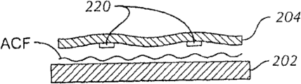
Fig. 2 A illustrates according to the utility model embodiment, the top view of exemplary first attachment area on the flexible circuit of Figure 1B.In the example of Fig. 2 A, first attachment area 204 can utilize anisotropic conductive film (ACF) to be attached to touch sensor panel 202 downwards, and this can form conduction and connect between conductor on first attachment area and the liner on the touch sensor panel.Because utilize pressure that first attachment area 204 is attached to touch sensor panel 202, so during connecting, some ACF may be extruded and, as shown in 226.Among the very important touch-screen embodiment of the optical clarity of touch sensor panel 202, wish to make the amount of the ACF that in the connection process, is extruded to reduce to minimum, therein so that it can not enter the zone of the substantially transparent of touch sensor panel.
The side view of exemplary first attachment area 204 of Fig. 2 B explanation on flexible circuit 200 with first conductor arrangement.In the example of Fig. 2 B, to lean on too closely if active conductor 220 is spaced apart, the space between the conductor may be not enough to hold ACF 226, thus excessive ACF may be extruded in the zone of the substantially transparent that enters touch sensor panel.
The side view of exemplary first attachment area 204 of Fig. 2 C explanation on flexible circuit 200 with second conductor arrangement.In the example of Fig. 2 C, if active conductor 220 is spaced apart too far apart, then first attachment area 204 (can be formed by flexible base film) may be pressed downward and fill the most of space between the conductor, thereby similarly, the space between the conductor may be not enough to hold ACF 226.Therefore, excessive ACF may be extruded in the zone of the substantially transparent that enters touch sensor panel once more.
Fig. 2 D illustrates according to embodiment of the present utility model, the side view of exemplary first attachment area 204 on the flexible circuit 200 with the 3rd conductor arrangement.In the example of Fig. 2 D, between active conductor 220, can form the no-load conductor 222 of specific quantity.The spacing of the quantity of no-load conductor 222 and no-load conductor and active conductor 220 can come (for example empiricism ground) to select according to the type of flexible circuit 200 and the cross sectional dimensions of thickness and conductor.By suitable selection conductor separation, can between conductor (no-load conductor and active conductor), keep enough intervals, so that most of ACF is retained in below first attachment area 204, make the amount minimum of the ACF that is extruded.
Fig. 3 explanation is according to embodiment of the present utility model, at the top view and the side view of the end of exemplary second attachment area shown in Figure 1B.In the example of Fig. 3, second attachment area 306 can comprise basement membrane 310 (for example polyamide), can form conductive trace layer 312 (for example electro-coppering) and insulator 314 (also being called overlayer or coverlay) on this basement membrane.Can obtain enough connection pressure endways with assurance by attached reinforcing member 328 in the end of second attachment area 306, this reinforcing member is also as sept.
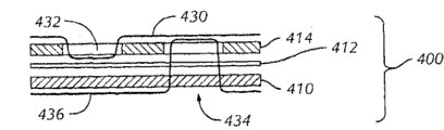
As mentioned above, need in basement membrane, form through hole and plating, so that set up electrical connection by through hole in the conventional flex circuits that all has trace on the two sides.On the two sides of flexible circuit, also all need insulator with protection formation conductive trace thereon.Because traditional flexible circuit has two-sided plating trace and double hyer insulation body and the whole thickness that increases, traditional double-sided flex circuit provides shielding for conductive trace.According to embodiment of the present utility model, for the shielding to the single-sided flexible circuit of enhancing is provided, can be at the attached thin conductive film in the two sides of flexible circuit.
Fig. 4 A explanation comprises the side view of the exemplary flexible circuit 400 of conducting film 430 according to embodiment of the present utility model on end face and optional bottom surface 436.Notice that Fig. 4 A does not draw in proportion, and has exaggerative size, this only is for purposes of illustration.In the example of Fig. 4 A, flexible circuit 400 can comprise basement membrane 410, can form conductive trace (for example copper) layer 412 and insulator 414 on this basement membrane.One or more conductive traces 412 can remain on set potential (for example).In one embodiment, can remain on set potential---such as ground---the particular conductivity trace on, form first opening (or groove) 432 in the insulator 414.Then can be on insulator 414 coating electrically conductive film 430, this conducting film can meet the shape of opening 432, and electrically contacts so that described conducting film remains on set potential with one or more traces in the described set potential trace.When conducting film 430 was maintained at set potential, it can be used as the shielding that is used for described conductive trace 412.
In another embodiment, before any conducting film of coating, also can form second opening (or groove) 434, this second opening passes basement membrane 410 and insulator 414, and avoids any conductive trace 412.Then can be on insulator 414 coating electrically conductive film 430, this conducting film can meet the shape of opening (or groove) 434, and electrically contacts so that described conducting film remains on set potential with one or more traces in the described set potential trace.Then can be on basement membrane 410 coating electrically conductive film 436, this conducting film can meet hole 434, and electrically contacts with conducting film 414 on opposite face.In this way, the conducting film on the two sides of flexible circuit all can remain on a set potential and conduct shielding.
Fig. 4 B explanation is according to the top view of the exemplary flexible circuit 400 of embodiment of the present utility model, and wherein this flexible circuit has opening 432 or 434 at least in insulator 414, so that at least one conducting film is remained on set potential.
Fig. 4 C explanation is according to the top view of the exemplary flexible circuit 400 of embodiment of the present utility model, and wherein this flexible circuit has groove 432 or 434 at least in insulator 414, so that at least one conducting film is remained on set potential.
Fig. 4 D explanation is according to the top view of the exemplary flexible circuit 400 of embodiment of the present utility model, and wherein this flexible circuit has another kind of groove 432 or 434 at least in insulator 414, so that at least one conducting film is remained on set potential.
Fig. 4 E explanation does not have the top view of the exemplary flexible circuit 400 of groove.According to embodiment of the present utility model, in the embodiment of Fig. 4 E, conducting film 430 and 436 extends beyond (stretching out) basement membrane 414, and stretches out in the zone by the conduction connection, so that two conducting films are all remained on set potential at this.
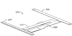
Fig. 5 A and 5B illustrate according to embodiment of the present utility model, the skeleton view of exemplary flexible circuit 500 under its manufacturing that flattens originally configuration.In the example of Fig. 5 A and 5B, flexible circuit 500 comprises first attachment area 504, and this first attachment area 504 comprises active conductor 520 and the no-load conductor 522 that forms along its length.Flexible circuit 500 also comprises second attachment area 506, and this second attachment area 506 can be included in the conductor 524 of its end.In the example of Fig. 5 A and 5B, flexible circuit 500 is formed by basement membrane 510, and comprises and only be formed on conductive trace on the visible base film surface and insulator (not shown) among Fig. 5 B.The afterbody 504 ' that integral body forms flexible circuit 500 parts comprises the afterbody conductor that is used to be connected to connector 538.
Fig. 6 explanation can comprise the exemplary computer system 600 of one or more the utility model embodiment described above.Computing system 600 can comprise one or more panel processor 602 and peripherals 604, and Panel subsystem 606.Peripherals 604 can include but not limited to the storer of random-access memory (ram) or other type or memory device, watchdog timer, or the like.Panel subsystem 606 can include but not limited to one or more sense channel 608, channel scan logic 610 and driver logic 614.Channel scan logic 610 can be carried out access to random access memory 612, independently from the sense channel reading of data, and provides control to sense channel.In addition, thereby also controllable driver logic 614 is with various frequencies and phase place generation pumping signal 616 for channel scan logic 610, and this pumping signal optionally is applied to the drive wire of touch sensor panel 624.In certain embodiments, Panel subsystem 606, panel processor 602 and peripherals 604 can be integrated in the single asic (ASIC).Among Fig. 6 615 is charge pumps.
Note, one or more in the function described above can be by being stored in that firmware in the storer (for example one of peripherals 604 of Fig. 6) be carried out and by panel processor 602 operations, perhaps is stored in the program storage 632 and by host-processor 628 operations.Described firmware also can be stored and/or transmit in any computer-readable medium, use together for instruction execution system, equipment or device use or and instruction executive system, equipment or device, described instruction execution system, equipment or device are such as the computer based system, the system that comprises processor, or other can take out the system of instruction and execution command from instruction execution system, equipment or device.In the context of the present specification, " computer-readable medium " can be anyly to comprise or store for instruction execution system, equipment or device uses or the medium of the program that and instruction executive system, equipment or device use together.Computer-readable medium can include but not limited to electricity, magnetic, light, electromagnetism, infrared or semiconductor system, equipment or device, portable computer diskette (magnetic), random-access memory (ram) (magnetic), ROM (read-only memory) (ROM) (magnetic), EPROM (Erasable Programmable Read Only Memory) (EPROM) (magnetic), portable optic disk such as CD, CD-R, CD-RW, DVD, DVD-R or DVD-RW, or the flash memory such as compact flash, safe digital card, USB memory storage, memory stick.
Described firmware also can be propagated in any transmission medium, use together for instruction execution system, equipment or device use or and instruction executive system, equipment or device, described instruction execution system, equipment or device are such as the computer based system, the system that comprises processor, or other can take out the system of instruction and execution command from instruction execution system, equipment or device.In the context of the present specification, " transmission medium " can be anyly to send, propagate or transmit for instruction execution system, equipment or device uses or the medium of the program that and instruction executive system, equipment or device use together.Described transmission computer-readable recording medium can include but not limited to electricity, magnetic, light, electromagnetism or infrared wired or wireless propagation medium.
Fig. 7 A illustrated example mobile phone 736, it can comprise touch sensor panel 724 and display device 730, utilizes the flexible circuit according to the utility model embodiment that described touch sensor panel is connected to Panel subsystem.
Fig. 7 B illustrated example digital media player 740, it can comprise touch sensor panel 724 and display device 730, utilizes the flexible circuit according to the utility model embodiment that described touch sensor panel is connected to Panel subsystem.By utilizing the described flexible circuit according to the utility model embodiment, that the mobile phone of Fig. 7 A and 7B and media player can be supported is littler, actual product more cheaply.
Though completely with reference to the accompanying drawings described embodiment of the present utility model, should be noted that variations and modifications will become apparent for those skilled in the art.Such variation and revise will be understood that it is to be included in the scope of the present utility model that claims limit.
Claims (20)
1. flexible circuit that is used to be connected to the two sides of touch sensor panel is characterized in that described flexible circuit comprises:
Be shaped as the basement membrane that forms first attachment area and second attachment area;
Conductive trace layer, wherein conductive trace is formed on the surface of described basement membrane and with the conductor in described first attachment area and second attachment area and stops, and described conductor is formed and positioned to being electrically connected with first of described touch sensor panel and second face; And
Be formed on the insulator on described conductive trace and the described conductor;
Wherein said basement membrane, described conductive trace and described insulator form and can be folded to be attached to first and second flexible overlapping of described touch sensor panel.
2. flexible circuit as claimed in claim 1, it is characterized in that, described flexible circuit also is included in active conductor and no-load conductor and the lower conductor on described second attachment area on described first attachment area, described lower conductor is arranged such that when described flexible circuit is folded and is attached to described touch sensor panel that with described active conductor and described no-load conductor described lower conductor does not face described active conductor and described no-load conductor.
3. flexible circuit as claimed in claim 1 is characterized in that, described flexible circuit comprises also and the integrally formed afterbody of described flexible circuit that described afterbody comprises the afterbody conductor that is used to be connected to logic card.
4. flexible circuit as claimed in claim 1, it is characterized in that, described flexible circuit also is included in active conductor and the no-load conductor on described first attachment area, one or more no-load conductors are placed in the described active conductor between per two active conductors in the wherein said no-load conductor, and described active conductor and described no-load conductor are spaced apart so that comprise the conduction attachment material that described first attachment area is attached to described touch sensor panel.
5. flexible circuit as claimed in claim 1 is characterized in that, described flexible circuit also comprises:
Lower conductor on described second attachment area, described insulator are configured to expose described lower conductor in each end of described second attachment area; And
Be formed on the reinforcing member of each end of described second attachment area, described reinforcing member and the lower conductor that is exposed are positioned on the direct relative face of end of described second attachment area, and described reinforcing member faces the lower conductor of described exposure.
6. flexible circuit as claimed in claim 1, it is characterized in that, described flexible circuit also comprises the top conductive film, and described top conductive film is formed on the end face of described flexible circuit and is connected to one or more conductive traces so that described top conductive film is remained on set potential.
7. flexible circuit as claimed in claim 6 is characterized in that, described flexible circuit comprises that also being formed on being used in the described insulator provides first opening of the connection from described top conductive film to described one or more conductive traces.
8. flexible circuit as claimed in claim 7, it is characterized in that, described flexible circuit also comprises the bottom conductive film, and described bottom conductive film is formed on the bottom surface of described flexible circuit and is connected to one or more conductive traces so that described bottom conductive film is remained on set potential.
9. flexible circuit as claimed in claim 6, it is characterized in that, described flexible circuit also comprises the bottom conductive film on the bottom surface that is formed on described flexible circuit, and described top conductive film and described bottom conductive film stretch out described flexible circuit, and is connect by conduction in stretching out the zone.
10. flexible circuit as claimed in claim 1 is characterized in that, described flexible circuit is bonded in the computing system and is connected between described touch sensor panel and the Panel subsystem, and wherein said computing system is bonded in the mobile device.
11. the system of the electrical connection on a two sides that is used to be provided to touch sensor panel is characterized in that described system comprises:
Be used on a surface of basement membrane, providing the device of conductive trace; And
Be used to provide the device that is shaped as the described basement membrane that forms first attachment area and second attachment area, wherein be folded when being attached to first of described touch sensor panel and second when described basement membrane and described conductive trace, described first attachment area and described second attachment area can with the pad alignment on first and second of described touch sensor panel.
12. system as claimed in claim 11 is characterized in that, described system also comprises the device that is used for providing insulator on described conductive trace.
13. system as claimed in claim 11, it is characterized in that, described system also comprises the active conductor that is used to be provided on described first attachment area and the device of no-load conductor and the lower conductor on described second attachment area, described lower conductor is arranged such that when flexible circuit is folded and be attached to described touch sensor panel that with described active conductor and described no-load conductor described lower conductor does not face described active conductor and described no-load conductor.
14. system as claimed in claim 13 is characterized in that, described system also comprises the device that is used to provide the afterbody that integrally forms with described flexible circuit, and described afterbody comprises the afterbody conductor that is used to be connected to logic card.
15. system as claimed in claim 11 is characterized in that, described system also comprises:
Be used for providing on described first attachment area device of active conductor and no-load conductor, wherein one or more no-load conductors are placed between each active conductor; And
Be used to provide active conductor spaced apart and no-load conductor to comprise the device that is used for described first attachment area is attached to the conduction attachment material of described touch sensor panel fully.
16. system as claimed in claim 14 is characterized in that, described system also comprises:
Be used on described second attachment area, providing the device of lower conductor;
Be used to provide and be restricted to the device that exposes the insulator of described lower conductor in each end of described second attachment area; And
Be used for providing in each end of described second attachment area the device of reinforcing member, described reinforcing member and the lower conductor that is exposed are positioned on the direct relative face of end of described second attachment area, and described reinforcing member faces the lower conductor of described exposure.
17. system as claimed in claim 14 is characterized in that, described system also comprises:
Be used on the end face of described flexible circuit, providing the device of top conductive film; And
Be used to provide the described top conductive film that is connected to one or more conductive traces described top conductive film is remained on the device of set potential.
18. system as claimed in claim 17 is characterized in that, described system also comprises and is used for providing first opening at insulator, so that the device from described top conductive film to the connection of described one or more conductive traces to be provided.
19. system as claimed in claim 18 is characterized in that, described system also comprises:
Be used to be provided at the device of the bottom conductive film that forms on the bottom surface of described flexible circuit; And
Be used to provide the described bottom conductive film that is connected to one or more conductive traces, described bottom conductive film is remained on the device of set potential.
20. system as claimed in claim 18 is characterized in that, described system also comprises:
Be used on the bottom surface of described flexible circuit, providing the device of bottom conductive film;
Be used to provide the described top conductive film that stretches out described flexible circuit and the device of described bottom conductive film; And
Be used for being provided at and stretch out the described top conductive film that zone conduction connects and the device of described bottom conductive film.
Applications Claiming Priority (2)
| Application Number | Priority Date | Filing Date | Title |
|---|---|---|---|
| US12/122,441 US8456851B2 (en) | 2008-05-16 | 2008-05-16 | Flex circuit with single sided routing and double sided attach |
| US12/122,441 | 2008-05-16 |
Publications (1)
| Publication Number | Publication Date |
|---|---|
| CN201540549U true CN201540549U (en) | 2010-08-04 |
Family
ID=40886444
Family Applications (2)
| Application Number | Title | Priority Date | Filing Date |
|---|---|---|---|
| CN2009201496009U Expired - Lifetime CN201540549U (en) | 2008-05-16 | 2009-05-15 | Flexible circuit and system providing electric connection to two sides of panel of touch sensor |
| CN200910139062XA Active CN101581995B (en) | 2008-05-16 | 2009-05-15 | Flex circuit with single sided routing and double sided attach |
Family Applications After (1)
| Application Number | Title | Priority Date | Filing Date |
|---|---|---|---|
| CN200910139062XA Active CN101581995B (en) | 2008-05-16 | 2009-05-15 | Flex circuit with single sided routing and double sided attach |
Country Status (7)
| Country | Link |
|---|---|
| US (2) | US8456851B2 (en) |
| EP (2) | EP2277102B1 (en) |
| JP (1) | JP5118100B2 (en) |
| KR (1) | KR101376459B1 (en) |
| CN (2) | CN201540549U (en) |
| HK (1) | HK1153558A1 (en) |
| WO (1) | WO2009140258A1 (en) |
Cited By (2)
| Publication number | Priority date | Publication date | Assignee | Title |
|---|---|---|---|---|
| CN107580406A (en) * | 2012-07-12 | 2018-01-12 | 环球展览公司 | To provide the component of the electrical connection of non-boundary flexible display and associated method |
| CN108541319A (en) * | 2015-11-20 | 2018-09-14 | 艾戴克斯公司 | The electronic sensor of support on the rigid substrate |
Families Citing this family (56)
| Publication number | Priority date | Publication date | Assignee | Title |
|---|---|---|---|---|
| US8456851B2 (en) * | 2008-05-16 | 2013-06-04 | Apple Inc. | Flex circuit with single sided routing and double sided attach |
| CN102802497B (en) * | 2009-06-25 | 2015-03-25 | 奥林巴斯医疗株式会社 | Image Pickup Unit |
| JP5300684B2 (en) * | 2009-10-27 | 2013-09-25 | 株式会社ジャパンディスプレイウェスト | Capacitance input device, method of manufacturing capacitance input device, and electro-optical device with input function |
| JP5455034B2 (en) * | 2009-12-09 | 2014-03-26 | ホシデン株式会社 | Flexible wiring board |
| KR101083084B1 (en) * | 2009-12-14 | 2011-11-16 | (주)필스 | Electrode connector and film speaker |
| TWI450237B (en) * | 2010-01-14 | 2014-08-21 | Wintek Corp | Touch-sensing display device |
| KR101703503B1 (en) * | 2010-07-13 | 2017-02-08 | (주)멜파스 | Touch sensing panel and touch sensing device for transmitting touch signal by using printed circuit board |
| KR101373047B1 (en) * | 2010-09-07 | 2014-03-11 | 삼성디스플레이 주식회사 | Flexible Printed Circuit Board and Touch Screen Panel Device Having the Same |
| US8982062B2 (en) * | 2011-05-09 | 2015-03-17 | Blackberry Limited | Multi-modal user input device |
| US8711570B2 (en) | 2011-06-21 | 2014-04-29 | Apple Inc. | Flexible circuit routing |
| US8337216B1 (en) * | 2011-07-26 | 2012-12-25 | Apple Inc. | Touch sensor back plane ground connection |
| US9024891B2 (en) | 2011-11-03 | 2015-05-05 | Synaptics Incorporated | Single substrate touch sensor |
| CN105138172B (en) * | 2011-11-27 | 2018-08-07 | 宸鸿科技(厦门)有限公司 | Touch sensing device and its manufacturing method |
| US9083344B2 (en) * | 2012-02-01 | 2015-07-14 | Apple Inc. | Touch sensor with integrated signal bus extensions |
| US9316677B2 (en) * | 2012-02-29 | 2016-04-19 | Apple Inc. | Devices and methods for testing flex cable shielding |
| US8907231B2 (en) | 2012-07-18 | 2014-12-09 | Nokia Corporation | Display arrangement |
| KR20140026129A (en) * | 2012-08-24 | 2014-03-05 | 삼성전기주식회사 | Flexible printed circuit board and touch panel having the same |
| US20140069696A1 (en) * | 2012-09-11 | 2014-03-13 | Apple Inc. | Methods and apparatus for attaching multi-layer flex circuits to substrates |
| CN103780803A (en) * | 2012-10-23 | 2014-05-07 | 鸿富锦精密工业(深圳)有限公司 | Image capturing module |
| JP6301056B2 (en) | 2012-12-21 | 2018-03-28 | 三菱電機株式会社 | Electronics |
| CN103246399A (en) * | 2013-05-07 | 2013-08-14 | 深圳欧菲光科技股份有限公司 | Printed circuit board and touch screen induction module comprising same |
| CN103338582A (en) * | 2013-05-20 | 2013-10-02 | 业成光电(深圳)有限公司 | Soft circuit board, and electronic device with same |
| CN104185367A (en) * | 2013-05-24 | 2014-12-03 | 英业达科技有限公司 | Flexible printed circuit board and circuit board structure applying flexible printed circuit board |
| US9448666B2 (en) | 2013-06-08 | 2016-09-20 | Microsoft Technology Licensing, Llc | Dark film lamination for a touch sensor |
| CN103309537A (en) * | 2013-06-18 | 2013-09-18 | 苏州市健邦触摸屏技术有限公司 | Capacitive touch screen |
| KR20160011196A (en) | 2013-09-20 | 2016-01-29 | 애플 인크. | Pressure-sensing stages for lamination systems |
| CN104635968A (en) * | 2013-11-09 | 2015-05-20 | 宝宸(厦门)光学科技有限公司 | Touch panel and touch module |
| US9372587B2 (en) | 2013-11-26 | 2016-06-21 | Synaptics Incorporated | Methods and apparatus for arranging electrode layers and associated routing traces in a sensor device |
| CN203775513U (en) * | 2013-12-30 | 2014-08-13 | 昆山维信诺显示技术有限公司 | Flexible circuit board |
| JP5813799B2 (en) * | 2014-02-13 | 2015-11-17 | 株式会社ジャパンディスプレイ | Touch panel and display device with touch panel |
| EP4218580A1 (en) | 2014-10-31 | 2023-08-02 | Irhythm Technologies, Inc. | Wireless physiological monitoring device and systems |
| WO2016174983A1 (en) * | 2015-04-28 | 2016-11-03 | シャープ株式会社 | Flexible substrate, touch panel sensor sheet module, and method for producing flexible substrate |
| CN104869752A (en) * | 2015-06-02 | 2015-08-26 | 合肥京东方光电科技有限公司 | Flexible circuit board, detection device thereof, detection method and display device |
| KR102394723B1 (en) | 2015-09-30 | 2022-05-09 | 엘지디스플레이 주식회사 | Touch screen panel and display device comprising the same |
| KR102446999B1 (en) * | 2016-02-01 | 2022-09-22 | 엘지이노텍 주식회사 | Printed circut board and touch window comprising the same |
| US10162194B2 (en) * | 2016-03-01 | 2018-12-25 | Verily Life Sciences Llc | Eye mountable device and flexible assembly for fabrication thereof |
| JP6199471B1 (en) * | 2016-10-31 | 2017-09-20 | 日本航空電子工業株式会社 | Connector assembly |
| KR102316563B1 (en) * | 2017-05-22 | 2021-10-25 | 엘지디스플레이 주식회사 | Organic Light-Emitting Display device having an upper substrate formed by a metal and Method of fabricating the same |
| JP6548703B2 (en) * | 2017-09-08 | 2019-07-24 | 三菱電機株式会社 | Electronics |
| DE102017220105A1 (en) * | 2017-11-10 | 2019-05-16 | Mahle International Gmbh | Electromagnetic control system |
| EP3602236A1 (en) * | 2017-12-05 | 2020-02-05 | Google LLC | Shielding a bending portion of a flexible display |
| KR102481250B1 (en) | 2018-03-08 | 2022-12-26 | 삼성디스플레이 주식회사 | Display device |
| CN108551721A (en) * | 2018-06-20 | 2018-09-18 | 业成科技(成都)有限公司 | Flexible circuit board and its bending-type electronics module of application |
| US11107841B2 (en) * | 2018-07-04 | 2021-08-31 | Samsung Electronics Co., Ltd. | Display panel and large format display apparatus using the same |
| KR102517268B1 (en) | 2018-07-16 | 2023-04-03 | 삼성전자주식회사 | Display panel |
| US11119616B2 (en) * | 2018-11-01 | 2021-09-14 | Apple Inc. | Trace transfer techniques for touch sensor panels with flex circuits |
| US11853515B2 (en) | 2018-12-19 | 2023-12-26 | Apple Inc. | Ultra-thin touch sensors |
| CN110636688B (en) * | 2019-08-21 | 2020-10-16 | 武汉华星光电半导体显示技术有限公司 | Flexible display device |
| JP2021086380A (en) * | 2019-11-27 | 2021-06-03 | 双葉電子工業株式会社 | Touch panel |
| KR20230119036A (en) | 2020-02-12 | 2023-08-14 | 아이리듬 테크놀로지스, 아이엔씨 | Non-invasive cardiac monitor and methods of using recorded cardiac data to infer a physiological characteristic of a patient |
| US11552344B2 (en) * | 2020-02-28 | 2023-01-10 | Gentherm Gmbh | Flex foil substrate connector for sensing battery voltage and temperature |
| JP2021153116A (en) * | 2020-03-24 | 2021-09-30 | 株式会社写真化学 | Wiring board and wiring method |
| US11350865B2 (en) | 2020-08-06 | 2022-06-07 | Irhythm Technologies, Inc. | Wearable device with bridge portion |
| CA3188343A1 (en) * | 2020-08-06 | 2022-02-10 | Jeff ABERCROMBIE | Electrical components for physiological monitoring device |
| US11650704B2 (en) | 2021-08-02 | 2023-05-16 | Tpk Advanced Solutions Inc. | Bonding structure and electronic device |
| US11880521B2 (en) | 2021-08-17 | 2024-01-23 | Tpk Touch Solutions (Xiamen) Inc. | Electronic device and method of manufacturing the same |
Family Cites Families (60)
| Publication number | Priority date | Publication date | Assignee | Title |
|---|---|---|---|---|
| JPS6144494A (en) * | 1984-08-09 | 1986-03-04 | ソニー株式会社 | Electric connector |
| US4715928A (en) * | 1985-09-27 | 1987-12-29 | Hamby Bill L | Flexible printed circuits and methods of fabricating and forming plated thru-holes therein |
| US4902236A (en) | 1988-11-14 | 1990-02-20 | E. I. Du Pont De Nemours And Company | Flex circuit and cable assembly |
| JPH0521901Y2 (en) | 1990-05-28 | 1993-06-04 | ||
| US5483261A (en) | 1992-02-14 | 1996-01-09 | Itu Research, Inc. | Graphical input controller and method with rear screen image detection |
| US5488204A (en) | 1992-06-08 | 1996-01-30 | Synaptics, Incorporated | Paintbrush stylus for capacitive touch sensor pad |
| US5880411A (en) | 1992-06-08 | 1999-03-09 | Synaptics, Incorporated | Object position detector with edge motion feature and gesture recognition |
| US5461202A (en) * | 1992-10-05 | 1995-10-24 | Matsushita Electric Industrial Co., Ltd. | Flexible wiring board and its fabrication method |
| JPH0945183A (en) * | 1995-08-01 | 1997-02-14 | Hitachi Aic Inc | Touch panel |
| US5825352A (en) | 1996-01-04 | 1998-10-20 | Logitech, Inc. | Multiple fingers contact sensing method for emulating mouse buttons and mouse operations on a touch sensor pad |
| US5835079A (en) | 1996-06-13 | 1998-11-10 | International Business Machines Corporation | Virtual pointing device for touchscreens |
| JP3219140B2 (en) | 1997-10-14 | 2001-10-15 | ソニーケミカル株式会社 | Electrical and electronic equipment |
| US6310610B1 (en) | 1997-12-04 | 2001-10-30 | Nortel Networks Limited | Intelligent touch display |
| US6235551B1 (en) * | 1997-12-31 | 2001-05-22 | Micron Technology, Inc. | Semiconductor device including edge bond pads and methods |
| US8479122B2 (en) | 2004-07-30 | 2013-07-02 | Apple Inc. | Gestures for touch sensitive input devices |
| US7663607B2 (en) | 2004-05-06 | 2010-02-16 | Apple Inc. | Multipoint touchscreen |
| KR100595920B1 (en) | 1998-01-26 | 2006-07-05 | 웨인 웨스터만 | Method and apparatus for integrating manual input |
| JP4015257B2 (en) | 1998-02-20 | 2007-11-28 | 株式会社小糸製作所 | Vehicle lamp |
| DE19820414A1 (en) * | 1998-05-07 | 1999-11-18 | Carmen Diessner | Contacting device |
| US6188391B1 (en) | 1998-07-09 | 2001-02-13 | Synaptics, Inc. | Two-layer capacitive touchpad and method of making same |
| JP4542637B2 (en) | 1998-11-25 | 2010-09-15 | セイコーエプソン株式会社 | Portable information device and information storage medium |
| US6449836B1 (en) * | 1999-07-30 | 2002-09-17 | Denso Corporation | Method for interconnecting printed circuit boards and interconnection structure |
| US6747290B2 (en) | 2000-12-12 | 2004-06-08 | Semiconductor Energy Laboratory Co., Ltd. | Information device |
| TW508562B (en) | 2001-01-10 | 2002-11-01 | Atouch Co Ltd | A contact structure of touch panel |
| US6985764B2 (en) * | 2001-05-03 | 2006-01-10 | Masimo Corporation | Flex circuit shielded optical sensor |
| JP3800984B2 (en) | 2001-05-21 | 2006-07-26 | ソニー株式会社 | User input device |
| JP2003173237A (en) | 2001-09-28 | 2003-06-20 | Ricoh Co Ltd | Information input-output system, program and storage medium |
| JP2003110207A (en) | 2001-09-28 | 2003-04-11 | Alps Electric Co Ltd | Flexible substrate |
| JP2003108302A (en) | 2001-10-01 | 2003-04-11 | Matsushita Electric Ind Co Ltd | Transparent touch panel |
| CN1205555C (en) | 2001-11-12 | 2005-06-08 | 联想(北京)有限公司 | Hard disk data backup and restore method |
| US6690387B2 (en) | 2001-12-28 | 2004-02-10 | Koninklijke Philips Electronics N.V. | Touch-screen image scrolling system and method |
| AU2002338134A1 (en) * | 2001-12-29 | 2003-07-15 | Xuanming Shi | A touch control display screen with a built-in electromagnet induction layer of septum array grids |
| US6969806B2 (en) * | 2002-05-28 | 2005-11-29 | Lockheed Martin Corporation | Cable and method |
| JP4090939B2 (en) | 2002-05-29 | 2008-05-28 | ニッタ株式会社 | Capacitive sensor and manufacturing method thereof |
| US11275405B2 (en) | 2005-03-04 | 2022-03-15 | Apple Inc. | Multi-functional hand-held device |
| KR100480154B1 (en) | 2002-08-30 | 2005-04-06 | 엘지.필립스 엘시디 주식회사 | Touch Panel |
| CN2567694Y (en) | 2002-09-16 | 2003-08-20 | 台均实业有限公司 | Touch control display screen with conductor lattice electromagnetic induction layer in it |
| JP3871991B2 (en) * | 2002-09-30 | 2007-01-24 | Smk株式会社 | Touch panel |
| KR100451775B1 (en) | 2002-12-31 | 2004-10-08 | 엘지.필립스 엘시디 주식회사 | Touch panel |
| JP4136695B2 (en) | 2003-02-10 | 2008-08-20 | 住友電工プリントサーキット株式会社 | Flexible printed circuit board |
| JP4163054B2 (en) * | 2003-06-23 | 2008-10-08 | アルプス電気株式会社 | Input device |
| EP1645172A4 (en) * | 2003-06-26 | 2009-06-24 | Formation Inc | Environmental protection of serial ata and other electronic devices |
| JP2005158811A (en) * | 2003-11-20 | 2005-06-16 | Alps Electric Co Ltd | Wireless lan unit |
| US7108515B2 (en) * | 2004-02-26 | 2006-09-19 | Matsushita Electric Industrial Co., Ltd. | Wiring board with bending section |
| JP3857278B2 (en) * | 2004-04-06 | 2006-12-13 | Smk株式会社 | Touch panel input device |
| JP4306590B2 (en) * | 2004-11-05 | 2009-08-05 | セイコーエプソン株式会社 | Electro-optical device and electronic apparatus |
| JP4591157B2 (en) * | 2005-03-31 | 2010-12-01 | パナソニック株式会社 | Wiring board, input device using the same, and manufacturing method thereof |
| JP2007088129A (en) * | 2005-09-21 | 2007-04-05 | Citizen Watch Co Ltd | Flexible circuit-board mounting body |
| JP2007165707A (en) * | 2005-12-15 | 2007-06-28 | Nitto Denko Corp | Flexible wiring circuit board |
| US7645941B2 (en) * | 2006-05-02 | 2010-01-12 | Multi-Fineline Electronix, Inc. | Shielded flexible circuits and methods for manufacturing same |
| GB2451210B8 (en) | 2006-06-09 | 2011-03-02 | Apple Inc | Touch screen liquid crystal display. |
| JP5273330B2 (en) * | 2006-08-04 | 2013-08-28 | 株式会社ジャパンディスプレイ | Display device |
| JP2008052874A (en) | 2006-08-28 | 2008-03-06 | Sony Corp | Magnetic tape driving device |
| KR100821043B1 (en) * | 2006-09-22 | 2008-04-08 | 삼성에스디아이 주식회사 | Flexilble Printed Circuit Board |
| JP2008091797A (en) * | 2006-10-04 | 2008-04-17 | Olympus Corp | Jointing device of flexible substrate |
| US8026903B2 (en) | 2007-01-03 | 2011-09-27 | Apple Inc. | Double-sided touch sensitive panel and flex circuit bonding |
| US7920129B2 (en) | 2007-01-03 | 2011-04-05 | Apple Inc. | Double-sided touch-sensitive panel with shield and drive combined layer |
| US8456851B2 (en) | 2008-05-16 | 2013-06-04 | Apple Inc. | Flex circuit with single sided routing and double sided attach |
| JP5455034B2 (en) * | 2009-12-09 | 2014-03-26 | ホシデン株式会社 | Flexible wiring board |
| CN103246399A (en) * | 2013-05-07 | 2013-08-14 | 深圳欧菲光科技股份有限公司 | Printed circuit board and touch screen induction module comprising same |
-
2008
- 2008-05-16 US US12/122,441 patent/US8456851B2/en active Active
-
2009
- 2009-05-12 WO PCT/US2009/043592 patent/WO2009140258A1/en active Application Filing
- 2009-05-12 EP EP09747342.5A patent/EP2277102B1/en active Active
- 2009-05-12 EP EP15164081.0A patent/EP2930598A1/en not_active Withdrawn
- 2009-05-12 KR KR1020107028185A patent/KR101376459B1/en active IP Right Grant
- 2009-05-15 CN CN2009201496009U patent/CN201540549U/en not_active Expired - Lifetime
- 2009-05-15 JP JP2009136681A patent/JP5118100B2/en active Active
- 2009-05-15 CN CN200910139062XA patent/CN101581995B/en active Active
-
2011
- 2011-01-05 US US12/985,274 patent/US8549738B2/en active Active
- 2011-07-22 HK HK11107619.3A patent/HK1153558A1/en unknown
Cited By (3)
| Publication number | Priority date | Publication date | Assignee | Title |
|---|---|---|---|---|
| CN107580406A (en) * | 2012-07-12 | 2018-01-12 | 环球展览公司 | To provide the component of the electrical connection of non-boundary flexible display and associated method |
| CN108541319A (en) * | 2015-11-20 | 2018-09-14 | 艾戴克斯公司 | The electronic sensor of support on the rigid substrate |
| CN108541319B (en) * | 2015-11-20 | 2022-11-01 | 傲迪司威生物识别公司 | Electronic sensor supported on rigid substrate |
Also Published As
| Publication number | Publication date |
|---|---|
| JP2010009594A (en) | 2010-01-14 |
| US8549738B2 (en) | 2013-10-08 |
| WO2009140258A1 (en) | 2009-11-19 |
| KR20110020826A (en) | 2011-03-03 |
| HK1153558A1 (en) | 2012-03-30 |
| CN101581995B (en) | 2013-03-27 |
| EP2277102A1 (en) | 2011-01-26 |
| KR101376459B1 (en) | 2014-03-19 |
| US20090283300A1 (en) | 2009-11-19 |
| US8456851B2 (en) | 2013-06-04 |
| EP2930598A1 (en) | 2015-10-14 |
| CN101581995A (en) | 2009-11-18 |
| EP2277102B1 (en) | 2016-11-02 |
| JP5118100B2 (en) | 2013-01-16 |
| US20110094670A1 (en) | 2011-04-28 |
Similar Documents
| Publication | Publication Date | Title |
|---|---|---|
| CN201540549U (en) | Flexible circuit and system providing electric connection to two sides of panel of touch sensor | |
| US10877615B2 (en) | Reducing the border area of a device | |
| CN201489505U (en) | Touch sensor panel, mobile phone and digital media player | |
| US9626061B2 (en) | PET-based touch pad | |
| CN101566895B (en) | Brick layout and stackup for touch screen | |
| US8711108B2 (en) | Direct connect single layer touch panel | |
| EP3101516A1 (en) | In cell touch panel and display device | |
| US8878081B2 (en) | Touch panel and display device having the same with second connector attached to a second side of the substrate | |
| US9128574B2 (en) | Touch screen panel | |
| US9830028B2 (en) | In-cell touch panel with self-capacitive electrodes and display device | |
| US20170153724A1 (en) | Touch panel module with conductive through holes and touch display device having the same | |
| TWI585725B (en) | Display device | |
| CN109116606B (en) | Display screen, manufacturing method of display screen and electronic equipment | |
| CN104076965A (en) | Touch display device | |
| US9933868B2 (en) | Flexible touch sensor | |
| CN109256035B (en) | Display screen, manufacturing method of display screen and electronic equipment |
Legal Events
| Date | Code | Title | Description |
|---|---|---|---|
| C14 | Grant of patent or utility model | ||
| GR01 | Patent grant | ||
| CX01 | Expiry of patent term |
Granted publication date: 20100804 |
|
| CX01 | Expiry of patent term |