CN1992337A - Silicon carbide bipolar transistor with silicon carbide collector layer and method of fabricating thereof - Google Patents
Silicon carbide bipolar transistor with silicon carbide collector layer and method of fabricating thereof Download PDFInfo
- Publication number
- CN1992337A CN1992337A CNA2006100642032A CN200610064203A CN1992337A CN 1992337 A CN1992337 A CN 1992337A CN A2006100642032 A CNA2006100642032 A CN A2006100642032A CN 200610064203 A CN200610064203 A CN 200610064203A CN 1992337 A CN1992337 A CN 1992337A
- Authority
- CN
- China
- Prior art keywords
- silicon carbide
- layer
- carborundum
- epitaxial
- conductivity type
- Prior art date
- Legal status (The legal status is an assumption and is not a legal conclusion. Google has not performed a legal analysis and makes no representation as to the accuracy of the status listed.)
- Pending
Links
- 229910010271 silicon carbide Inorganic materials 0.000 title claims abstract description 303
- HBMJWWWQQXIZIP-UHFFFAOYSA-N silicon carbide Chemical compound [Si+]#[C-] HBMJWWWQQXIZIP-UHFFFAOYSA-N 0.000 title claims abstract description 167
- 238000004519 manufacturing process Methods 0.000 title abstract description 12
- 238000002161 passivation Methods 0.000 claims abstract description 83
- 238000000034 method Methods 0.000 claims abstract description 17
- 230000012010 growth Effects 0.000 claims description 37
- 239000000758 substrate Substances 0.000 claims description 21
- VYPSYNLAJGMNEJ-UHFFFAOYSA-N Silicium dioxide Chemical compound O=[Si]=O VYPSYNLAJGMNEJ-UHFFFAOYSA-N 0.000 claims description 18
- 238000002347 injection Methods 0.000 claims description 17
- 239000007924 injection Substances 0.000 claims description 17
- 239000000377 silicon dioxide Substances 0.000 claims description 9
- 235000012239 silicon dioxide Nutrition 0.000 claims description 8
- XUIMIQQOPSSXEZ-UHFFFAOYSA-N Silicon Chemical compound [Si] XUIMIQQOPSSXEZ-UHFFFAOYSA-N 0.000 abstract description 3
- 229910052710 silicon Inorganic materials 0.000 abstract description 3
- 239000010703 silicon Substances 0.000 abstract description 3
- 239000004065 semiconductor Substances 0.000 description 11
- 238000005516 engineering process Methods 0.000 description 10
- 239000000463 material Substances 0.000 description 10
- 229910052751 metal Inorganic materials 0.000 description 10
- 239000002184 metal Substances 0.000 description 9
- 230000006798 recombination Effects 0.000 description 9
- 238000005215 recombination Methods 0.000 description 9
- IJGRMHOSHXDMSA-UHFFFAOYSA-N Atomic nitrogen Chemical compound N#N IJGRMHOSHXDMSA-UHFFFAOYSA-N 0.000 description 8
- 239000002019 doping agent Substances 0.000 description 8
- 230000014509 gene expression Effects 0.000 description 7
- 229910001218 Gallium arsenide Inorganic materials 0.000 description 5
- 239000013078 crystal Substances 0.000 description 5
- 238000000407 epitaxy Methods 0.000 description 4
- 229910052757 nitrogen Inorganic materials 0.000 description 4
- 230000015556 catabolic process Effects 0.000 description 3
- 239000002800 charge carrier Substances 0.000 description 3
- 230000002950 deficient Effects 0.000 description 3
- 238000000151 deposition Methods 0.000 description 3
- 230000008021 deposition Effects 0.000 description 3
- PXHVJJICTQNCMI-UHFFFAOYSA-N Nickel Chemical compound [Ni] PXHVJJICTQNCMI-UHFFFAOYSA-N 0.000 description 2
- 229910052581 Si3N4 Inorganic materials 0.000 description 2
- 229910004298 SiO 2 Inorganic materials 0.000 description 2
- 239000004411 aluminium Substances 0.000 description 2
- 229910052782 aluminium Inorganic materials 0.000 description 2
- XAGFODPZIPBFFR-UHFFFAOYSA-N aluminium Chemical compound [Al] XAGFODPZIPBFFR-UHFFFAOYSA-N 0.000 description 2
- 238000000137 annealing Methods 0.000 description 2
- 238000005229 chemical vapour deposition Methods 0.000 description 2
- 238000010276 construction Methods 0.000 description 2
- 238000010586 diagram Methods 0.000 description 2
- 238000005530 etching Methods 0.000 description 2
- 238000003780 insertion Methods 0.000 description 2
- 230000037431 insertion Effects 0.000 description 2
- 150000002500 ions Chemical class 0.000 description 2
- 239000002905 metal composite material Substances 0.000 description 2
- 239000000203 mixture Substances 0.000 description 2
- HQVNEWCFYHHQES-UHFFFAOYSA-N silicon nitride Chemical compound N12[Si]34N5[Si]62N3[Si]51N64 HQVNEWCFYHHQES-UHFFFAOYSA-N 0.000 description 2
- ZOXJGFHDIHLPTG-UHFFFAOYSA-N Boron Chemical compound [B] ZOXJGFHDIHLPTG-UHFFFAOYSA-N 0.000 description 1
- 229910019001 CoSi Inorganic materials 0.000 description 1
- GPXJNWSHGFTCBW-UHFFFAOYSA-N Indium phosphide Chemical compound [In]#P GPXJNWSHGFTCBW-UHFFFAOYSA-N 0.000 description 1
- 101150034459 Parpbp gene Proteins 0.000 description 1
- HZEWFHLRYVTOIW-UHFFFAOYSA-N [Ti].[Ni] Chemical compound [Ti].[Ni] HZEWFHLRYVTOIW-UHFFFAOYSA-N 0.000 description 1
- 230000004913 activation Effects 0.000 description 1
- 238000005275 alloying Methods 0.000 description 1
- UQZIWOQVLUASCR-UHFFFAOYSA-N alumane;titanium Chemical compound [AlH3].[Ti] UQZIWOQVLUASCR-UHFFFAOYSA-N 0.000 description 1
- REDXJYDRNCIFBQ-UHFFFAOYSA-N aluminium(3+) Chemical compound [Al+3] REDXJYDRNCIFBQ-UHFFFAOYSA-N 0.000 description 1
- 230000015572 biosynthetic process Effects 0.000 description 1
- 229910052796 boron Inorganic materials 0.000 description 1
- 238000003763 carbonization Methods 0.000 description 1
- 239000003795 chemical substances by application Substances 0.000 description 1
- 239000011248 coating agent Substances 0.000 description 1
- 238000000576 coating method Methods 0.000 description 1
- 229910017052 cobalt Inorganic materials 0.000 description 1
- 239000010941 cobalt Substances 0.000 description 1
- GUTLYIVDDKVIGB-UHFFFAOYSA-N cobalt atom Chemical compound [Co] GUTLYIVDDKVIGB-UHFFFAOYSA-N 0.000 description 1
- 230000000295 complement effect Effects 0.000 description 1
- 238000002425 crystallisation Methods 0.000 description 1
- 230000008025 crystallization Effects 0.000 description 1
- 230000001186 cumulative effect Effects 0.000 description 1
- 238000006731 degradation reaction Methods 0.000 description 1
- 238000000280 densification Methods 0.000 description 1
- 238000009792 diffusion process Methods 0.000 description 1
- 230000005684 electric field Effects 0.000 description 1
- 230000002349 favourable effect Effects 0.000 description 1
- PCHJSUWPFVWCPO-UHFFFAOYSA-N gold Chemical compound [Au] PCHJSUWPFVWCPO-UHFFFAOYSA-N 0.000 description 1
- 239000010931 gold Substances 0.000 description 1
- 229910052737 gold Inorganic materials 0.000 description 1
- 238000000227 grinding Methods 0.000 description 1
- 238000002513 implantation Methods 0.000 description 1
- 230000005527 interface trap Effects 0.000 description 1
- 229910052759 nickel Inorganic materials 0.000 description 1
- 230000005855 radiation Effects 0.000 description 1
- 229910052594 sapphire Inorganic materials 0.000 description 1
- 239000010980 sapphire Substances 0.000 description 1
- 229920006395 saturated elastomer Polymers 0.000 description 1
- 229910021332 silicide Inorganic materials 0.000 description 1
- FVBUAEGBCNSCDD-UHFFFAOYSA-N silicide(4-) Chemical compound [Si-4] FVBUAEGBCNSCDD-UHFFFAOYSA-N 0.000 description 1
- 239000007787 solid Substances 0.000 description 1
Images


Classifications
-
- H—ELECTRICITY
- H01—ELECTRIC ELEMENTS
- H01L—SEMICONDUCTOR DEVICES NOT COVERED BY CLASS H10
- H01L29/00—Semiconductor devices adapted for rectifying, amplifying, oscillating or switching, or capacitors or resistors with at least one potential-jump barrier or surface barrier, e.g. PN junction depletion layer or carrier concentration layer; Details of semiconductor bodies or of electrodes thereof ; Multistep manufacturing processes therefor
- H01L29/02—Semiconductor bodies ; Multistep manufacturing processes therefor
- H01L29/12—Semiconductor bodies ; Multistep manufacturing processes therefor characterised by the materials of which they are formed
- H01L29/16—Semiconductor bodies ; Multistep manufacturing processes therefor characterised by the materials of which they are formed including, apart from doping materials or other impurities, only elements of Group IV of the Periodic System
- H01L29/1608—Silicon carbide
-
- H—ELECTRICITY
- H01—ELECTRIC ELEMENTS
- H01L—SEMICONDUCTOR DEVICES NOT COVERED BY CLASS H10
- H01L29/00—Semiconductor devices adapted for rectifying, amplifying, oscillating or switching, or capacitors or resistors with at least one potential-jump barrier or surface barrier, e.g. PN junction depletion layer or carrier concentration layer; Details of semiconductor bodies or of electrodes thereof ; Multistep manufacturing processes therefor
- H01L29/02—Semiconductor bodies ; Multistep manufacturing processes therefor
- H01L29/06—Semiconductor bodies ; Multistep manufacturing processes therefor characterised by their shape; characterised by the shapes, relative sizes, or dispositions of the semiconductor regions ; characterised by the concentration or distribution of impurities within semiconductor regions
- H01L29/10—Semiconductor bodies ; Multistep manufacturing processes therefor characterised by their shape; characterised by the shapes, relative sizes, or dispositions of the semiconductor regions ; characterised by the concentration or distribution of impurities within semiconductor regions with semiconductor regions connected to an electrode not carrying current to be rectified, amplified or switched and such electrode being part of a semiconductor device which comprises three or more electrodes
- H01L29/1004—Base region of bipolar transistors
-
- H—ELECTRICITY
- H01—ELECTRIC ELEMENTS
- H01L—SEMICONDUCTOR DEVICES NOT COVERED BY CLASS H10
- H01L29/00—Semiconductor devices adapted for rectifying, amplifying, oscillating or switching, or capacitors or resistors with at least one potential-jump barrier or surface barrier, e.g. PN junction depletion layer or carrier concentration layer; Details of semiconductor bodies or of electrodes thereof ; Multistep manufacturing processes therefor
- H01L29/66—Types of semiconductor device ; Multistep manufacturing processes therefor
- H01L29/68—Types of semiconductor device ; Multistep manufacturing processes therefor controllable by only the electric current supplied, or only the electric potential applied, to an electrode which does not carry the current to be rectified, amplified or switched
- H01L29/70—Bipolar devices
- H01L29/72—Transistor-type devices, i.e. able to continuously respond to applied control signals
- H01L29/73—Bipolar junction transistors
- H01L29/732—Vertical transistors
- H01L29/7325—Vertical transistors having an emitter-base junction leaving at a main surface and a base-collector junction leaving at a peripheral surface of the body, e.g. mesa planar transistor
Abstract
A bipolar junction transistor (BJT) includes a silicon carbide (SiC) collector layer of first conductivity type, as epitaxial silicon carbide base layer of second conductivity type on the silicon carbide collector layer, and an epitaxial silicon carbide emitter mesa of the first conductivity type on the epitaxial silicon carbide base layer. An epitaxial silicon cacbite passivation layer of the first conductivity type is provided on at least a portion of the epitaxial silicon carbide base layer outside the silicon carbide emitter mesa. The epitaxial silicon carbide passivation layer can be configured to deplete fully at zero device bias. Related fabrication methods also are disclosed.
Description
The governmental interests statement
The present invention produces under the support of the contract number W911NF-04-2-0022 that is authorized by U.S. military strength research laboratory (ARL).Government has certain power to the present invention.
Technical field
The present invention relates to the correlation technique of power semiconductor and manufacturing semiconductor power device, more specifically, relate to the correlation technique of silicon carbide power device and manufacturing silicon carbide power device.
Background technology
Power device is widely used in transmitting big electric current and/or supports high voltage.Traditional power device is made by single-crystal semiconductor material usually.One type power device is bipolar junction transistor (BJT).BJT is a power device known and commonly used.BJT typically comprises the semi-conducting material with two relative p-n junctions close to each other.Therefore, BJT can be called " n-p-n " or " p-n-p " transistor.
At work, current carrier enters the first conductive-type semiconductor material sections with one of them adjacency of p-n junction, and it is called as emitter.Most electric charge carrier leaves device from the semiconductor material region in abutting connection with first conductivity type of another p-n junction, and it is called as collector electrode.The fraction semi-conducting material that is used as base stage is between collector and emitter, and it has second conductivity type opposite with first conductivity type of collector and emitter.Two kinds of p-n junctions of this of BJT are formed on collector electrode and base stage part and base stage and the emitter part of meeting of meeting.
When electric current is injected into base stage or when base stage is extracted, depends on that BJT is n-p-n or p-n-p, the electric charge carrier that can move to collector electrode from emitter is that flowing of electronics or hole can be affected.Typically, the little electric current that is applied to base stage can be controlled the bigger electric current by BJT pari passu, makes its element for electronic circuit effective.Structure and the operational detail of BJT have been discussed in the Solid State Electronic Device by B.Streetman (second edition (1980), the 7th chapter) work, have been introduced its full content here as a reference.
The material that constitutes device can influence the operability and the validity of device.For example, traditional BJT is typically formed by silicon (Si), but also can comprise GaAs (GaAs) and indium phosphide (InP).Carborundum (SiC) also is used as the material of BJT.SiC has potential favourable characteristic of semiconductor, for example broad stopband, high electric field breakdown strengths, high-termal conductivity, high-melting-point and high saturated electron drift velocity.Therefore, with respect to the device that for example forms among the Si at other semi-conducting material, the electronic device that forms in SiC can have under higher temperature, in higher power density, with more speed, with the higher power level and/or the ability of working under high radiation density.
Because the ability of under high-frequency, high temperature and/or high power levels, working, for example be used for radar and communicate by letter, be used for high-power switchgear use and be used for high-temperature operation for example the application of the high frequency transmitter of jet aircraft engine control be starved of the SiC transistor.Therefore, produce the SiC of device quality and the method for the device that formed by SiC becomes scientists and engineers's point of interest in decades.
SiC is to surpass 150 different polymorphic type or crystal structure crystallizations, and wherein modal is 3C, 4H and 6H, wherein " C " expression " cubical " and " H " expression " six sides' ".SiC normally is difficult to be used in the material of semiconductor device.Especially, the high-melting-point of SiC can be so that technology, and for example the diffusion of alloying and dopant is more difficult because operate so required many other materials easily be used under the high temperature of SiC breakdown.SiC also is extremely hard material, and in fact the most frequently used purposes of SiC is a grinding agent.Although the difficulty that these are possible has been utilized SiC to make to finish, diode, transistor and other device.
For example, in people's such as Palmour U.S. Patent No. 4,945,394, SiC BJT has been discussed, has introduced its full content here as a reference.As discussed here, SiC BJT has emitter and the base stage of utilizing the high temperature ion to inject to form trap.And, in the U.S. Patent No. 6,218,254 of Singh etc., SiC BJT has been discussed also, introduce its full content here as a reference.As discussed herein, use epitaxial growth and high temperature ion to inject and form SiC BJT with base stage and emitter.Singh has further discussed with removable dielectric gap wall to improve the aligning of base region and emitter region.
SiC BJT can comprise that also at least one is used for the highly doped injection region of base stage and/or emitter.The formation of injection region can produce the SiC crystal and destroy.For example, owing to inject the surface recombination current of the defective generation that causes, can reduce the current gain of device.Because the stacking fault the base region that can produce from the defective that injection technology produces, the function that the current gain of device can be used as the time is reduced.And the highly doped emitter region that exists in these devices may have the poor life-span, and it can further reduce the current gain of device.
With reference now to Fig. 1,, the sectional view of traditional SiC BJT will be discussed.As shown in fig. 1, at highly doped N
+Provide N on the SiC substrate 114
-SiC extension (epi) collector layer 116.N
+SiC substrate 114 and N
-SiC epi collector layer 116 can be defined for the collector electrode 110 of device.At N
-P-type (P) SiC epi base layer 120 is provided on the SiC epi collector layer 116.As shown in fig. 1, on p-type SiC base layer 120, provide n-type epi emitter platform 130 (N
+).Emitter platform 130 can be by optionally epitaxial growth and/or epitaxial growth and etching subsequently form.And, highly doped (P
+) district 124 can be formed in the base layer 120 by injection technique.Especially, P
+The injection of base region 124 can have the aluminium ion (Al of energy from about 20keV to about 360keV using under about 1100 ℃ temperature from about 650 ℃
+) carry out.As mentioned above, this injection can cause the damage to the SiC crystal, and its can not annealed by high-temperature activation (1600-1700 ℃) removed fully.
Especially, can produce surface recombination current and cause forming stacking fault by injecting the defective of introducing in the base layer of device.This relation is represented by equation:
β=i
C/i
B
Wherein β represents current gain, i
CThe expression collector current, i
BThe expression base current.Base current i
BCan further be expressed as
i
B=i
Br+i
Bi+i
Bsr;
I wherein
BrBe recombination current, i
BiThe majority carrier that expression is injected across emitter junction, and i
BsrThe presentation surface recombination current.Current gain can be represented by equation:
β=i
C/(i
Br+i
Bi+i
Bsr)
Therefore, the surface recombination current i in the base region
BsrAny increase can produce lower current gain to device.
Refer again to Fig. 1, passivated dielectric medium layer 140 is provided on device surface.Passivated dielectric medium layer 140 can comprise silicon dioxide and/or silicon nitride.BJT further comprises base stage (B) contact 122, and emitter (E) contact 132 contacts 112 with collector electrode (C).Can provide by N
+114,130 and P
+The high-doped zone of 124 expressions is to improve the quality of ohmic contact.Base stage, emitter and collector contact 122,132 and 112 can comprise the sandwich construction of ohmic metal and/or cover layer metal respectively.Other embodiment that is to be understood that bipolar transistor can eliminate one or more floor and/or district as shown in Figure 1, maybe can increase additional district and/or floor.
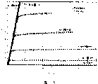
Unfortunately, for example have been found that as shown in fig. 1 that the current gain of SiC BJT can reduce along with the time under typical operating conditions.Especially, Fig. 2 A-2D has illustrated the output characteristic of the SiC BJT of the cumulative stress with the increase that has continued 0 minute, 15 minutes, 30 minutes and 16 hours under 10A respectively.Occurred the current gain reduction within 15 minutes work, the later output characteristic of Fig. 2 A-2D shows continuous reduction.
Summary of the invention
Bipolar junction transistor according to some embodiments of the invention (BJT) comprises the carborundum collector layer of first conductivity type, in the epitaxial silicon carbide base layer of second conductivity type different on the carborundum collector layer with away from the epitaxial silicon carbide emitter platform of first conductivity type of carborundum collector layer on the silica-based utmost point layer of extension with first conductivity type.The epitaxial silicon carbide passivation layer of first conductivity type is provided at least a portion of the epitaxial silicon carbide base layer outside carborundum emitter platform.
In certain embodiments, the epitaxial silicon carbide passivation layer of first conductivity type has the carrier concentration of first conductivity type and has a thickness, exhausts epitaxial silicon carbide passivation layer fully by the epitaxial silicon carbide base layer when wherein selecting carrier concentration and thickness with the zero-bias on bipolar junction transistor.More particularly, in certain embodiments, the silicon carbide passivation layer of first conductivity type has the carrier concentration C of first conductivity type and has the thickness T of selecting according to equation:
Wherein q is an elementary charge, ε
sIt is the dielectric constant of carborundum.
Epitaxial silicon carbide passivation layer can have multiple extension on base layer, can extend to the emitter platform by a plurality of embodiment according to the present invention.For example, in certain embodiments, epitaxial silicon carbide emitter platform comprise with the epitaxial silicon carbide base layer away from end face, and the sidewall that between this end face and epitaxial silicon carbide base layer, extends.At some embodiment, epitaxial silicon carbide passivation layer is at least a portion of the epitaxial silicon carbide base layer outside the carborundum platform but do not extend on sidewall.In other embodiments, epitaxial silicon carbide passivation layer is also at sidewall but be not to extend on end face.In other embodiments, epitaxial silicon carbide passivation layer is also extended on end face.
And, can provide multiple extension for the epitaxial silicon carbide passivation layer of first conductivity type on carborundum base stage layer.Particularly, in certain embodiments, carborundum base stage layer comprises first and has the more second portion of high carrier concentration from emitter platform splitting ratio first.In certain embodiments, epitaxial silicon carbide passivation layer extends to contiguous second portion from contiguous carborundum platform on the silicon carbide-based utmost point layer of extension.In other embodiments, epitaxial silicon carbide passivation layer extends to second portion from adjacent carbonization silicon emitter platform.In other embodiments, passivation layer extends to contiguous second portion from carborundum emitter platform.In another embodiment, passivation layer extends to second portion from the carborundum platform.The second portion of base layer can form by injecting the first that separates from the emitter platform, and/or can be the epitaxial-base platform in the first that separates from the emitter platform.
In another embodiment, the passivated dielectric medium layer can provide on epitaxial silicon carbide passivation layer away from the epitaxial silicon carbide base layer.The passivated dielectric medium layer can comprise silicon dioxide.And, in certain embodiments, epitaxial silicon carbide emitter platform can comprise the first of contiguous epitaxial silicon carbide base layer and in the first and on the second portion away from the epitaxial silicon carbide base layer, wherein second portion has the carrier concentration higher than first.At last, in other embodiments, can use individual layer and/or sandwich construction to provide collector electrode, base stage and emitter to contact.
Bipolar junction transistor can be according to various embodiments of the present invention, by the carborundum base stage layer of epitaxial growth second conductivity type on the first conductive silicon carbide collector layer different with second conductivity type and on carborundum base stage layer the carborundum emitter platform of epitaxial growth first conductivity type make.The epitaxial growth at least a portion on the carborundum base stage layer of carborundum emitter platform outside of the silicon carbide passivation layer of first conductivity type.These are epitaxially grown any or all ofly can to adopt that to cover growth, cover after the growth be selective etch, and/or selective epitaxial growth.In certain embodiments, carrier concentration and/or silicon carbide passivation layer thickness can provide as mentioned above.And the extension of silicon carbide passivation layer can provide with aforesaid any one.
In another embodiment of the present invention, the district of the carrier concentration higher than silicon carbide base region is injected in the carborundum base stage floor, and separate with the emitter platform, the epitaxial growth silicon carbide passivation layer is to extend to the district that is injected into from contiguous carborundum emitter platform on carborundum base stage floor.In another embodiment, on carborundum base stage layer and with the emitter platform, separate the base stage platform of epitaxial growth second conductivity type, the epitaxial growth silicon carbide passivation layer with on the silicon carbide-based utmost point layer of extension from contiguous carborundum emitter platform to contiguous but extend with base stage platform divided portion.On silicon carbide passivation layer, form the passivated dielectric medium layer.
Therefore, can comprise silicon carbide substrates and at least a portion of base region and the epitaxial silicon carbide passivation layer of the conductivity type opposite with the base region, this substrate comprises emitter, base stage and collector area according to the bipolar junction transistor of some embodiments of the present invention.Epitaxial silicon carbide passivation layer can be provided with to exhaust fully under the zero-bias on the bipolar junction transistor.The passivated dielectric medium layer also can provide on the silicon carbide passivation layer away from the base region.The extension of silicon carbide passivation layer can be as mentioned above.
Description of drawings
Fig. 1 is the sectional view of carborundum (SiC) bipolar junction transistor (BJT).
Fig. 2 A-2D has illustrated the reduction of traditional Si C BJT along with the time current gain with figure.
Fig. 3 is the sectional view according to the SiC BJT of various embodiments of the present invention.
Fig. 4 is the sectional view of the SiC BJT of the potential cause that descends of explanation current gain.
Fig. 5-the 10th is according to the sectional view of the SiC BJT of various embodiments of the present invention.
Figure 11 is the flow chart that can carry out making with various embodiments according to the present invention the operation of SiC BJT.
Embodiment
The present invention more fully describes referring now to accompanying drawing, wherein shows the present invention.Yet the present invention can be with many multi-form embodiments, and should not be construed as limited to described here.More definite, these embodiment are provided so that this specification more comprehensively with complete and scope of the present invention pass on fully to those skilled in the art.In the accompanying drawings, for clear floor and district's ground size and the relative size can exaggerated.
Be to be understood that when element or layer be called as " on ", " being connected to " or " being coupled to " another element or when layer, it can be directly last, connects or be coupled to other element maybe to have insertion element or layer.On the contrary, when element is called as " directly on ", " being directly connected to " or " directly being coupled to " another element or layer, there are not insertion element or layer.Identical from the beginning to the end Reference numeral is represented components identical.As used herein, term " and/or " comprise any one of the relevant project of listing or one or more combinations.
Be to be understood that in the whole text, though can use first, second grade of term describing multiple element, parts, district, floor and/or part here, these elements, parts, district, floor and/part should not limit by these terms.These terms only are used for an element, parts, district, floor or part and other element, parts, district, floor or section are distinguished.Therefore, first element of discussing below, parts, district, floor or part can be known as second element, parts, district, floor or part under the situation that does not break away from the technology of the present invention.
And, can use here relative terms for example " bottom " or " bottom " and " top " or " top " to describe the element described in figure and the relation of another element.Be to be understood that relative terms want to comprise with figure in the different device direction of direction described.For example, if the device among the figure has been reversed, the element on the D score side of other element of description will be positioned at this other element " on " on the side.Therefore the exemplary term D score, can comprise " bottom " and " top " direction, depends on the concrete direction of figure.Similarly, if the device in a figure has been reversed, be described as other element " bottom " or " ... under " element can be positioned at then this other element " on ".Exemplary term " bottom " or " ... under " therefore can comprise " and ... on " and " ... under " two kinds.
As used herein, term " vicinity " meaning is that an element extends near another element, and it comprises closely and separating, contacts and/or covers another element.On the contrary, when element be described to extend " arrive " another element or " from " during another element extension, the meaning is that in fact this element contacts or covered this another element, does not comprise the situation that this element separates from another element.
Hereinafter with reference is described embodiments of the invention as the sectional view that desirable embodiment of the present invention schematically illustrates.Similarly, from the variant that the expression of this specification draws, for example, manufacturing technology and/or tolerance limit (tolerance) are expected.Therefore, embodiments of the invention should not be construed as limited to the given shape in zone described herein, and should comprise from for example making the variant in shape that obtains.For example, be described as the injection region of rectangle, typically have feature rounding or crooked and/or have the gradient of implantation concentration at its edge, rather than from being injected into the sudden change of non-injection region.Similarly, can obtain some injections in the district between buried region and the surface of injecting by injecting the buried region that forms.Therefore, Shuo Ming district is actually schematically in the drawings, and their shape also is not inclined to the accurate shape in district of explanation device, and is not inclined to and limits the scope of the invention.
Unless there have in addition to be now fixed, all terms used herein (comprising technology and scientific terminology) have by the identical meanings under the present invention of one of those skilled in the art common sense.Should further understand term, for example in the general dictionary that uses, show those fixed terms, should be interpreted as having in the context with correlation technique and this specification their consistent implication of implication, and should do not explained, unless here limit especially with desirable or excessive formal meaning.
With reference to the concrete polarity conductivity type that is used for a plurality of floor/district embodiments of the invention are described.Yet, skilled person in the art will appreciate that the polarity of distinguishing floor can be reversed to provide the device of opposite polarity.For example, term " first conductivity type " and " second conductivity type " refer to opposite conductivity type for example n or p type, yet, describe here and each embodiment of illustrating also comprises the embodiment that it is complementary.
BJT is active, the three terminal semiconductor device that comprise two very approaching back-to-back p-n junctions particularly.BJT shows as n-p-n or p-n-p widely, depends on the conductivity type of their corresponding base polar regions, collector area and emitter region.Though be appreciated that n-p-n type BJT only has been discussed in the whole text, embodiments of the invention are not limited to this structure.For example, without departing from the present invention,, also can provide the p-n-p transistor by reversing described conductivity type.And BJT structure described here can repeat so that power device to be provided, so that structure described here can provide whole power device or be used for the unit cell of power device.
The doped region that one skilled in the art will appreciate that carborundum can form by epitaxial growth and/or by injecting.For example, the p type district of carborundum can be by forming in growth under the situation that p type dopant is arranged or by inject p type dopant in unadulterated p type or n type epitaxial loayer.The structure that obtains from epitaxial growth is different with the structure that obtains from injection.Therefore, term " epitaxial loayer/district " and " implanted layer/district " structurally are different from silicon carbide layer/district, and can be used to the enumerating of architectural feature in the floor/district of carborundum here, or are used to form the enumerating of method in the floor/district of carborundum.For example in the U.S. Patent No. 5,011,549 and 4,912 of Kong etc., the manufacturing of SiC epitaxial loayer has been discussed in 064, introduce its full content here as a reference, just as they have been set forth in full.
Some embodiments of the present invention provide the bipolar junction transistor (BJT) of (SiC) base region that has epitaxial silicon carbide and multilayer epitaxial emitter region.The use of the epitaxial sic base region among the BJT according to some embodiments of the invention can be cancelled injecting and the needs of subsequently high annealing, and described technology can cause the damage of SiC crystal and the reducing of current gain that cause device thus.Therefore, BJT according to some embodiments of the invention can have the current gain of improvement with respect to traditional devices.And, use multilayer epitaxial SiC emitter region that the current gain of device is improved further.Yet other embodiments of the invention can be used the high conductivity base region of individual layer extension emitter region and/or injection.
With reference now to Fig. 3,, BJT sectional view according to some embodiments of the invention will be discussed.As shown in Figure 3, can provide carborundum (SiC) substrate 314.The polarity of substrate 314 can be n-type or the p type SiC with many types of for example 3C, 2H, 4H or 15R.For the purpose of example, the device according to discussing in the embodiment of the invention illustrated in fig. 3 comprises n type SiC substrate 314.As shown in Figure 3, substrate 314 is highly doped n type SiC (N
+).As used herein, " P
+" or " N
+" refer to the district that limits by the higher carrier concentration of concentration than the charge carrier that exists in the vicinity of substrate or identical or another floor or other district.Similarly, " P
-" or " N
-" refer to the district that limits by than the lower carrier concentration of carrier concentration that exists in the vicinity of identical or another floor or other district.Substrate 314 can utilize n type dopant, and for example nitrogen mixes.Substrate can have from about 1.0 * 10
18Cm
-3To about 5.0 * 10
19Cm
-3Carrier concentration and thickness from about 200 μ m to about 500 μ m.
As further specifying among Fig. 3, on SiC substrate 314, provide epitaxial collector layer 316.Epitaxial collector layer 316 can utilize n type dopant, and for example nitrogen mixes.Epitaxial collector layer 316 can have from about 1.0 * 10
13Cm
-3To about 1.0 * 10
18Cm
-3Carrier concentration and thickness from about 1.0 μ m to about 250 μ m.Substrate 314 and epitaxial sic collector layer 316 can provide the collector electrode (C) 310 of BJT.Yet, in other embodiments, can use non-conductive substrate, collector layer 316 can provide collector electrode.Epitaxial base layer 320 is provided on the epitaxial collector layer 316 and can utilizes p type dopant for example aluminium or boron doping.Epitaxial base layer 320 can have from about 1.0 * 10
15Cm
-3To about 5.0 * 10
19Cm
-3Carrier concentration and thickness from about 0.1 μ m to about 10 μ m.
In certain embodiments, SiC base stage injection and/or extension contact zone 324 be provided at epitaxial base layer 320 and/or on.As shown in Figure 3, SiC base stage contact zone 324 can be infused in the silicon carbide epitaxy base layer 320.Yet in other embodiments, can grow on SiC epitaxial base layer 320 away from SiC epitaxial collector layer 316 in SiC base stage contact zone 324.In certain embodiments, the SiC base stage contact zone 324 of injection wherein can comprise non-homogeneous carrier concentration.And, in other embodiments, can provide concentration relatively uniformly as shown in Figure 3.
In other embodiments, can grow on carborundum base stage layer 320 in epitaxial silicon carbide base stage contact zone, will describe in detail below.In certain embodiments, epitaxial silicon carbide base stage contact zone can comprise individual layer.And in other embodiments, epitaxial sic base stage contact zone can be included in p type epitaxial sic district on the epitaxial base layer 320 and the 2nd p type epitaxial sic district in a p type epitaxial sic district.In certain embodiments, a p type epitaxial sic district has from about 1.0 * 10
18Cm
-3To about 1.0 * 10
19Cm
-3Carrier concentration and thickness from about 0.1 μ m to about 10 μ m.The 2nd p type epitaxial sic district has from about 1.0 * 10
19Cm
-3To about 5.0 * 10
20Cm
-3Carrier concentration and thickness from about 0.1 μ m to about 3.0 μ m.Epitaxial base layer 320 and injection/epitaxial sic base stage contact zone can provide base stage (B) district according to some embodiments of the present invention BJT.And in other embodiments, SiC base stage contact zone can be single p type district and in other embodiments, does not need to provide the base stage contact zone fully.
As further shown in Figure 3, on epitaxial base layer 320, provide epitaxial sic emitter platform 330.As described, epitaxial sic emitter platform 330 has n type conductivity.In certain embodiments, epitaxial sic emitter platform 330 has first (N) and the second (N respectively
+) part.In these embodiments, the first of epitaxial sic emitter platform can provide on epitaxial base layer 320, and can utilize for example nitrogen doping of n type dopant.The first of epitaxial sic emitter platform 330 can have from about 1.0 * 10
17Cm
-3To about 5 * 10
19Cm
-3Carrier concentration and thickness from about 0.1 μ m to about 5.0 μ m.The second portion of epitaxial sic emitter platform 330 can utilize n type dopant to mix, nitrogen for example, and can have the carrier concentration higher with respect to first.Particularly, the second portion 105 of epitaxial sic emitter region can have from about 5 * 10
18Cm
-3To about 5 * 10
20Cm
-3Carrier concentration and thickness from about 0.1 μ m to about 3.0 μ m.Therefore, according to some embodiments of the present invention, epitaxial sic emitter platform 330 comprises the low-doped n type layer of the injection efficiency that improvement can be provided and the highly doped n type layer of the contact surface of improvement can be provided.Yet in other embodiments, epitaxial silicon carbide emitter platform 330 can comprise single district as shown in Figure 3.Epitaxial silicon carbide emitter platform 330 can be by covering extension and etching and/or by the selective epitaxial growth manufacturing.
Comprise injection/epitaxial sic base region 324 and epitaxial sic emitter platform 330 though be to be understood that embodiments of the invention as shown in Figure 3, embodiments of the invention are not limited to this structure.For example, according to some embodiments of the present invention, under the situation that does not have the epitaxial sic base region, can provide to have first (N) and the second (N
+) part the epitaxial sic emitter region.
Other detailed design and the manufacture view of the SiC BJT of Fig. 3, forward part in this detail specifications is described, the sequence number that is provided at application on September 16th, 2005 is No.11/229,474, the application that is entitled as " Silicon Carbide Bipolar Junction Transistors Having Epitaxial Base regions andMultilayer Emitter and Methods of Fabrication the Same " of Agarwal etc. is introduced its full content here as a reference.
Still with reference to figure 3, at least a portion of the silicon carbide-based utmost point layer 320 of extension, provide N type epitaxial silicon carbide passivation layer 350 in carborundum emitter platform 330 outsides.Epitaxial silicon carbide passivation layer 350 can be considered to extend at least a portion of the outer surface of carborundum base stage layer 320, in carborundum emitter platform 330 outsides.Do not wishing under the situation about being limited by any work theory, because increase in surface recombination, as shown in Figure 4, for example is between the emitter 130 and base stage 120 of passivated dielectric medium layer 140 passivation of silicon dioxide layer of deposition/densification subsequently by heat growth silicon dioxide, can be created in the current gain shown in Fig. 2 A-2D and reduce.Owing to produce interface trap at the interface at silicon carbide/silicon dioxide, can produce surface recombination.
Sharp contrast, as shown in Figure 3, embodiments of the invention can provide the epitaxial silicon carbide passivation layer of first conductivity type at least a portion of the epitaxial silicon carbide base region of second conductivity type.In certain embodiments, the total electrical charge in this passivation layer 350 can be selected, so that when zero device is inclined to one side, because about 2.7 volts built-in electromotive force silicon carbide passivation layer 350 can be exhausted fully.Epitaxial silicon carbide surface passivation layer 350 can help to reduce or suppress surface recombination.The current gain shown in Fig. 2 A-2D reduce can be stopped or reduce effectively subsequently.In some embodiments of the invention, the epitaxial silicon carbide passivation layer of first conduction type has the carrier concentration C of first conduction type (being the n type) here and has the thickness T of selecting according to following equation:
Wherein q is an elementary charge (1.6 * 10
-19Enclosed pasture), ε
sIt is the dielectric constant of carborundum.
Continue the explanation of Fig. 3, passivated dielectric medium layer 340 is being provided on base layer 320 on the silicon carbide passivation layer 350 and/or on the extension emitter platform 330.Passivated dielectric medium layer 340 for example can comprise, heat growth silicon dioxide (SiO
2), chemical vapor deposition SiO
2And/or chemical vapor deposition silicon nitride (Si
3N
4).The ohmic metal that is suitable for n type carborundum can be provided on emitter platform 330.The ohmic metal of can annealing as further described below is to provide ohmic contact.Some embodiments of the present invention comprise conductive substrates 314.In these embodiment of the present invention, ohmic metal can provide on substrate 314 away from epitaxial collector layer 316.It will be appreciated by those skilled in the art that and to use non-conductive substrate to implement the present invention that for example semi-insulating silicon carbide or sapphire wherein can be provided for the ohmic metal of collector electrode on the surface of SiC collector layer 316.
Also can on base layer 320, provide the ohmic metal that is applicable to p type carborundum.Metal and/or metal composite go for ohmic contact.For example, nickel and titanium nickel composition are suitable for the ohmic contact to n type carborundum, and aluminium or aluminium titanium composition are suitable for the ohmic contact to p type carborundum.And, also can use cobalt silicide (CoSi
2) as the ohmic contact of p type carborundum.In U.S. Patent No. 5,323,022 and 5,409,859 have illustrated ohmic contact, introduce its full content here as a reference.Cover metal, for example gold also can be deposited on the ohmic contact to provide emitter, base stage and collector electrode to contact 332,322 and 312 respectively.Passivated dielectric medium layer 340 with contact 312,322 and 332 example design for example at the above-mentioned patent application serial numbers No.11/229 that quotes, be described in 474.
Term used herein " ohmic contact " refers to wherein in fact be provided by the relation of impedance=V/I the contact of associated impedance, wherein under the operating frequency (operating frequency all is identical basically in promptly relevant with ohmic contact impedance) and electric current of all expectations basically, V is the voltage of cross-over connection contact, and I is an electric current.
The scope of the epitaxial silicon carbide passivation layer 350 of Fig. 3 can different embodiment according to the subject invention and is changed.Particularly, in Fig. 3, epitaxial silicon carbide passivation layer 350 extends to base stage contact 322 from epitaxial silicon carbide emitter platform 330 on the silicon carbide-based utmost point layer 320 of extension.In contrast, in Fig. 5, epitaxial silicon carbide passivation layer 350a is adjacent with carborundum emitter platform 330, but separately extends with it, and also contact with base stage 322 adjacent, but separately extend with it.In Fig. 6, epitaxial silicon carbide passivation layer extends to carborundum emitter platform 330, adjacently separates extension with it but contact 322 with base stage.In other embodiments, not shown, epitaxial silicon carbide passivation layer 350b can extend near the carborundum emitter platform 330, but separates with it, and extends to base stage contact 322.
And in the embodiment of Fig. 7, epitaxial silicon carbide passivation layer 350c extends on the sidewall 330s of carborundum emitter platform 330 at least in part, but does not extend on the top 330t of emitter platform 330.At last, as shown in Figure 8, epitaxial silicon carbide passivation layer 350d also can extend on the 330t of platform top, except platform sidewall 320s or replace platform sidewall 320s.The combination and the subgroup that are to be understood that other extension of embodiment shown in Fig. 3 and the 5-8 and/or silicon carbide passivation layer are closed and can be provided according to some embodiments of the present invention.
Epitaxial silicon carbide passivation layer 350 and 350a-350d can utilize epitaxial deposition (cover and/optionally) manufacturing, with can be doped to first conductivity type with concentration C, thickness T can exhaust epitaxial silicon carbide passivation layer by epitaxial silicon carbide base layer 320 fully under zero device bias.When other layer of SiC BJT when having aforesaid thickness and doping content, silicon carbide passivation layer 350 and 350a-350d can be that 0.5 μ m is thick and have and reach about 1 * 10
16Cm
-3N type doping content.In other embodiments, can provide about 2 μ m thickness and reach about 8 * 10
14Cm
-3N type concentration.Therefore, the doping that thinner layer can be higher, vice versa, to satisfy above-mentioned equation and/or to exhaust silicon carbide passivation layer fully.
Fig. 9 is the sectional view according to the SiC BJT of other embodiments of the invention.Comparison diagram 8 and 9 provides aforesaid multilayer epitaxial carborundum emitter platform 330a, 330b.And, also be provided for ohmic contact layer 322a, 332a and the 312a that base stage 322, emitter 332 and collector electrode 312 contact as mentioned above respectively.As shown in Figure 9, insulated epitaxial silicon carbide layer 350d extends to high conduction and injects base stage contact zone 324, but does not extend to base stage ohmic contact regions 322a or arrive base stage contacting metal 322.Be to be understood that Fig. 9 embodiment can with any one or all combinations among other embodiment described here.
Figure 10 is the sectional view according to the SiC BJT of other embodiments of the invention.In these embodiments, the high conduction of epitaxial growth (P on base layer 320
+) the base stage contact zone to be to provide the epitaxial-base platform 1024 that separates with emitter platform 330.Base stage platform 1024 can comprise individual layer, as P among Figure 10
+Show, maybe can comprise a plurality of layer, for example the layer of the relative low electric conductivity (P) of contiguous base layer 320 with away from the relative high conductivity (P on the relative low electric conductivity layer of base region 320
+) layer, as mentioned above with at the above-mentioned patent application serial numbers No.11/229 that quotes, in 474.And, in Figure 10, epitaxial silicon carbide passivation layer 350e is shown is extending on the sidewall of emitter platform and the top and on base layer 320 contiguous but that separate with base stage platform 1024.Yet in other embodiments, insulated epitaxial silicon carbide layer 350e does not need to retract from base stage platform 1024.Be appreciated that Figure 10 embodiment can with any one or all combinations among other embodiment discussed here.
Figure 11 can carry out to make the workflow diagram of SiC BJT according to various embodiments of the present invention.With reference to Figure 11, at piece 1110, epitaxial growth carborundum collector electrode, base stage and emitter layer.For example, N
-Silicon carbide epitaxy collector layer 316 can epitaxial growth at N
+On the silicon carbide substrates 314, P silicon carbide epitaxy base layer 320 can be grown in N
-On the silicon carbide epitaxy collector layer 316, as mentioned above.Emitter platform and/or base stage platform can be by epitaxial growths.The epitaxial growth of carborundum collector electrode, base stage and the emitter layer of square 1110 is known for those skilled in the art, does not need further discussion here.
Yet, reference block 1120, silicon carbide passivation layer 350 and 350a-350e are by epitaxial growth.Covering extension can be with in certain embodiments.In other embodiments, can condition be set so that extension is easier does not grow at horizontal surface on vertical surface.In other embodiments, can produce optionally epitaxial deposition, wherein to for example using TaC and/or other known mask material to not wishing that carrying out epitaxially grown district shelters by using the mask blasnket area.These embodiment any one, also can use selective etch.The doping content of SiC passivation layer and thickness can be selected as mentioned above.
Then, in piece 1130, passivated dielectric medium layer 340 can use technology known in the art to form, and in piece 1140, forms contact.Be appreciated that also the order not as Figure 11 carries out the operation of piece 1110-1140.For example, forming passivated dielectric medium layer (piece 1130) before, can form contact (piece 1140).And, in other embodiments, before the operation of piece 1120, can carry out the operation of piece 1130 and/or 1140.
Therefore, according to the BJT of some embodiments of the present invention can provide comprise emitter region, base region and collector area and with the silicon carbide structure of the silicon carbide passivation layer of the conductivity type opposite of base region at least a portion of base region.The surface that should know silicon carbide layer can the passivation by forming silicon dioxide layer thereon, and it can reduce the interfacial state of energy level near the carborundum conduction band.Patent application serial numbers in application in 16 days September in 2005 of Das etc. is No.11/229,476, exercise question is introduced its full content here as a reference for having described some technology of making oxide skin(coating) on silicon carbide layer in " Ultra-Thin Ohmic Contacts For P-TpyeNitride Light Emitting Devices And Methods of Forming ".Yet, have been found that according to some embodiments of the present invention, wish to replace or except the dielectric silicon carbide passivation layer, provide epitaxial silicon carbide passivation layer, so that further suppress surface recombination, reduce or eliminate the reducing of current gain in undesirable past along with the time thus.Based on the emitter of the use ledge of the heterojunction bipolar transistor (HBT) of GaAs (GaAs) to suppress current gain degradation.Yet GaAs HBT emitter ledge technology can differentiate with embodiments of the invention according to the viewpoint of material, structure and/or manufacturing.
In drawing and description, embodiments of the invention are disclosed, though adopted concrete term, they only are used for general and purpose of description, scope of the present invention will be set forth at appended claims.
Claims (26)
1, a kind of bipolar junction transistor (BJT) comprising:
The carborundum collector layer of first conductivity type;
The epitaxial silicon carbide base layer of second conductivity type different on the carborundum collector layer with first conductivity type;
Epitaxial silicon carbide emitter platform away from first conductivity type on the epitaxial silicon carbide base layer of carborundum collector layer; With
The epitaxial silicon carbide passivation layer of first conductivity type at least a portion of the epitaxial silicon carbide base layer of carborundum emitter platform outside.
2, according to the BJT of claim 1, wherein the epitaxial silicon carbide passivation layer of first conductivity type has the carrier concentration of first conductivity type, and exhausts the thickness of epitaxial silicon carbide passivation layer when having selection with the zero-bias on BJT fully by the epitaxial silicon carbide base layer.
3, according to the BJT of claim 1, wherein the epitaxial silicon carbide passivation layer of first conductivity type has the carrier concentration C of first conductivity type and has the thickness T of selecting according to following equation:
Wherein q is an elementary charge, ε
sIt is the dielectric constant of carborundum.
4, according to the BJT of claim 1, wherein epitaxial silicon carbide emitter platform comprises away from the top of epitaxial silicon carbide base layer and the sidewall that extends between top and epitaxial silicon carbide base layer, and wherein epitaxial silicon carbide passivation layer is outside rather than extending at least a portion of the silicon carbide-based utmost point layer of extension on the sidewall at carborundum emitter platform.
5, according to the BJT of claim 1, wherein epitaxial silicon carbide emitter platform comprises away from the top of epitaxial silicon carbide base layer and the sidewall that extends between top and epitaxial silicon carbide base layer, and wherein epitaxial silicon carbide passivation layer is outside and extending at least a portion of the silicon carbide-based utmost point layer of extension on the sidewall rather than on the top at carborundum emitter platform.
6, according to the BJT of claim 1, wherein epitaxial silicon carbide emitter platform comprises away from the top of epitaxial silicon carbide base layer and the sidewall that extends between top and epitaxial silicon carbide base layer, wherein epitaxial silicon carbide passivation layer is in carborundum emitter platform outside, on the sidewall and on the top, at least a portion of the silicon carbide-based utmost point layer of extension, extend.
7, according to the BJT of claim 1, wherein the epitaxial silicon carbide base layer comprises first and the higher second portion of carrier concentration of the ratio first that separates with the emitter platform, and wherein epitaxial silicon carbide passivation layer extends to contiguous second portion from contiguous carborundum emitter platform on the silicon carbide-based utmost point layer of extension.
8, according to the BJT of claim 1, wherein the epitaxial silicon carbide base layer comprises first and the higher second portion of carrier concentration of the ratio first that separates with the emitter platform, and wherein epitaxial silicon carbide passivation layer extends to second portion from contiguous carborundum emitter platform on the silicon carbide-based utmost point layer of extension.
9, according to the BJT of claim 1, wherein the epitaxial silicon carbide base layer comprises first and the higher second portion of carrier concentration of the ratio first that separates with the emitter platform, and wherein epitaxial silicon carbide passivation layer extends to contiguous second portion from carborundum emitter platform on the silicon carbide-based utmost point layer of extension.
10, according to the BJT of claim 1, wherein the epitaxial silicon carbide base layer comprises first and the higher second portion of carrier concentration of the ratio first that separates with the emitter platform, and wherein epitaxial silicon carbide passivation layer extends to second portion from carborundum emitter platform on the silicon carbide-based utmost point layer of extension.
11, according to the BJT of claim 1, wherein the epitaxial silicon carbide base layer comprises first and separates in first and with the emitter platform and inject the carrier concentration higher than first, and wherein epitaxial silicon carbide passivation layer extends to this injection near carborundum emitter platform on the silicon carbide-based utmost point layer of extension.
12, according to the BJT of claim 1, further comprise with the emitter platform separate the epitaxial-base platform on the silicon carbide-based utmost point layer of extension and wherein epitaxial silicon carbide passivation layer on the silicon carbide-based utmost point layer of extension, extend to contiguous base stage platform but separate with the base stage platform from contiguous carborundum emitter platform.
13,, further comprise away from the passivated dielectric medium layer on the epitaxial silicon carbide passivation layer of second conductivity type of epitaxial silicon carbide base layer according to the BJT of claim 1.
14, according to the BJT of claim 13, wherein the passivated dielectric medium layer comprises silicon dioxide.
15, according to the BJT of claim 1, wherein epitaxial silicon carbide emitter platform comprises the first of contiguous epitaxial silicon carbide base layer and in first and away from the second portion of epitaxial silicon carbide base layer, wherein second portion has the carrier concentration higher than first.
16, according to the BJT of claim 1, further comprise:
The silicon carbide substrates of first conductivity type on the carborundum collector layer;
Collector electrode contact on silicon carbide substrates;
Base stage contact on the silicon carbide-based utmost point layer of extension; With
Emitter contact on epitaxial silicon carbide emitter platform.
17, make the method for bipolar junction transistor (BJT), comprising:
The carborundum base stage layer of epitaxial growth second conductivity type on the carborundum collector layer of first conductivity type, first conductivity type is different from second conductivity type;
The carborundum emitter platform of epitaxial growth first conductivity type on carborundum base stage layer; With
Silicon carbide passivation layer at carborundum emitter platform outside epitaxial growth first conductivity type at least a portion of carborundum base stage layer.
18, according to the method for claim 17, wherein epitaxial growth silicon carbide passivation layer comprises with the carrier concentration of first conductivity type with to select to exhaust fully by carborundum base stage layer when adding zero-bias on BJT the silicon carbide passivation layer of grown in thickness first conductivity type of epitaxial silicon carbide passivation layer.
19, according to the method for claim 17, wherein epitaxial growth silicon carbide passivation layer comprises the silicon carbide passivation layer of thickness T epitaxial growth first conductivity type of selecting with the carrier concentration C of first conductivity type with according to following equation:
Wherein q is an elementary charge, ε
sIt is the dielectric constant of carborundum.
20, according to the method for claim 17, further be included in the carborundum base stage floor and separate and inject than the carborundum base stage floor district of high carrier concentration more with the emitter platform, and wherein epitaxial growth silicon carbide passivation layer comprises the silicon carbide passivation layer of epitaxial growth first conductivity type, and it extends to from contiguous carborundum emitter platform on carborundum base stage floor and is injected into the district.
21, according to the method for claim 17, further be included in the base stage platform that separates epitaxial growth second conductivity type on carborundum base stage layer with the emitter platform, wherein epitaxial growth silicon carbide passivation layer comprises the silicon carbide passivation layer of epitaxial growth first conductivity type, and it extends to contiguous base stage platform from contiguous carborundum emitter platform but separates with the base stage platform on carborundum base stage layer.
22,, further be included in away from silicon carbide base region and on silicon carbide passivation layer, form the passivated dielectric medium layer according to the method for claim 17.
23, according to the method for claim 17, the carborundum base stage layer of epitaxial growth second conductivity type on the carborundum collector layer of first conductivity type different with second conductivity type wherein, step before is the carborundum collector layer of epitaxial growth first conductivity type on the silicon carbide substrates of first conductivity type.
24, a kind of bipolar junction transistor (BJT) comprising:
The silicon carbide structure that comprises emitter region, base region and collector area; With
The epitaxial silicon carbide passivation layer of the conductivity type opposite on the base region with the base region.
25, according to the BJT of claim 24, wherein the epitaxial silicon carbide passivation layer setting is to exhaust fully during in zero-bias on the BJT.
26,, further be included in away from the passivated dielectric medium layer of base region on epitaxial silicon carbide passivation layer according to the BJT of claim 25.
Applications Claiming Priority (2)
| Application Number | Priority Date | Filing Date | Title |
|---|---|---|---|
| US11/315,672 US7345310B2 (en) | 2005-12-22 | 2005-12-22 | Silicon carbide bipolar junction transistors having a silicon carbide passivation layer on the base region thereof |
| US11/315,672 | 2005-12-22 |
Publications (1)
| Publication Number | Publication Date |
|---|---|
| CN1992337A true CN1992337A (en) | 2007-07-04 |
Family
ID=37898628
Family Applications (1)
| Application Number | Title | Priority Date | Filing Date |
|---|---|---|---|
| CNA2006100642032A Pending CN1992337A (en) | 2005-12-22 | 2006-12-22 | Silicon carbide bipolar transistor with silicon carbide collector layer and method of fabricating thereof |
Country Status (5)
| Country | Link |
|---|---|
| US (1) | US7345310B2 (en) |
| EP (1) | EP1806787B1 (en) |
| JP (1) | JP5095989B2 (en) |
| CN (1) | CN1992337A (en) |
| AT (1) | ATE509372T1 (en) |
Cited By (9)
| Publication number | Priority date | Publication date | Assignee | Title |
|---|---|---|---|---|
| CN102097462A (en) * | 2009-10-22 | 2011-06-15 | 本田技研工业株式会社 | Bipolar semiconductor device and method of producing same |
| CN102362353A (en) * | 2009-03-24 | 2012-02-22 | 飞兆半导体公司 | Silicon carbide bipolar junction transistor |
| CN102610638A (en) * | 2012-03-22 | 2012-07-25 | 西安电子科技大学 | SiC-bipolar junction transistor (SiC-BJT) device for power integrated circuit and manufacturing method of SiC-BJT device |
| CN103748684A (en) * | 2011-05-16 | 2014-04-23 | 科锐 | SIC devices with high blocking voltage terminated by a negative bevel |
| CN105977287A (en) * | 2016-07-25 | 2016-09-28 | 电子科技大学 | Silicon carbide bipolar junction transistor |
| CN108110002A (en) * | 2017-12-18 | 2018-06-01 | 西安理工大学 | A kind of bipolar integrated transistors of complementary type SiC and preparation method thereof |
| CN108767005A (en) * | 2018-05-29 | 2018-11-06 | 金陵科技学院 | A kind of computer system |
| CN108899361A (en) * | 2018-07-11 | 2018-11-27 | 北京优捷敏半导体技术有限公司 | A kind of silicon carbide bipolar transistor npn npn and its manufacturing method |
| CN113437133A (en) * | 2021-06-22 | 2021-09-24 | 弘大芯源(深圳)半导体有限公司 | Power bipolar transistor resistant to secondary breakdown |
Families Citing this family (50)
| Publication number | Priority date | Publication date | Assignee | Title |
|---|---|---|---|---|
| US20060211210A1 (en) * | 2004-08-27 | 2006-09-21 | Rensselaer Polytechnic Institute | Material for selective deposition and etching |
| US7977154B2 (en) * | 2006-04-14 | 2011-07-12 | Mississippi State University | Self-aligned methods based on low-temperature selective epitaxial growth for fabricating silicon carbide devices |
| US7728402B2 (en) | 2006-08-01 | 2010-06-01 | Cree, Inc. | Semiconductor devices including schottky diodes with controlled breakdown |
| US8432012B2 (en) | 2006-08-01 | 2013-04-30 | Cree, Inc. | Semiconductor devices including schottky diodes having overlapping doped regions and methods of fabricating same |
| US8710510B2 (en) | 2006-08-17 | 2014-04-29 | Cree, Inc. | High power insulated gate bipolar transistors |
| US8835987B2 (en) | 2007-02-27 | 2014-09-16 | Cree, Inc. | Insulated gate bipolar transistors including current suppressing layers |
| JP5372002B2 (en) * | 2007-11-09 | 2013-12-18 | クリー インコーポレイテッド | A power semiconductor device having a mesa structure and a buffer layer including a mesa step |
| US9640609B2 (en) | 2008-02-26 | 2017-05-02 | Cree, Inc. | Double guard ring edge termination for silicon carbide devices |
| US7560325B1 (en) * | 2008-04-14 | 2009-07-14 | Semisouth Laboratories, Inc. | Methods of making lateral junction field effect transistors using selective epitaxial growth |
| US8232558B2 (en) | 2008-05-21 | 2012-07-31 | Cree, Inc. | Junction barrier Schottky diodes with current surge capability |
| US8097919B2 (en) | 2008-08-11 | 2012-01-17 | Cree, Inc. | Mesa termination structures for power semiconductor devices including mesa step buffers |
| WO2010024240A1 (en) * | 2008-08-26 | 2010-03-04 | 本田技研工業株式会社 | Bipolar silicon carbide semiconductor device and method for manufacturing same |
| WO2010024239A1 (en) * | 2008-08-26 | 2010-03-04 | 本田技研工業株式会社 | Junction semiconductor device and method for manufacturing same |
| US8465799B2 (en) * | 2008-09-18 | 2013-06-18 | International Business Machines Corporation | Method for preparation of flat step-free silicon carbide surfaces |
| US8497552B2 (en) | 2008-12-01 | 2013-07-30 | Cree, Inc. | Semiconductor devices with current shifting regions and related methods |
| US8294507B2 (en) | 2009-05-08 | 2012-10-23 | Cree, Inc. | Wide bandgap bipolar turn-off thyristor having non-negative temperature coefficient and related control circuits |
| US8637386B2 (en) | 2009-05-12 | 2014-01-28 | Cree, Inc. | Diffused junction termination structures for silicon carbide devices and methods of fabricating silicon carbide devices incorporating same |
| US8629509B2 (en) | 2009-06-02 | 2014-01-14 | Cree, Inc. | High voltage insulated gate bipolar transistors with minority carrier diverter |
| US8193848B2 (en) | 2009-06-02 | 2012-06-05 | Cree, Inc. | Power switching devices having controllable surge current capabilities |
| US8541787B2 (en) | 2009-07-15 | 2013-09-24 | Cree, Inc. | High breakdown voltage wide band-gap MOS-gated bipolar junction transistors with avalanche capability |
| US8354690B2 (en) | 2009-08-31 | 2013-01-15 | Cree, Inc. | Solid-state pinch off thyristor circuits |
| US9117739B2 (en) | 2010-03-08 | 2015-08-25 | Cree, Inc. | Semiconductor devices with heterojunction barrier regions and methods of fabricating same |
| US8415671B2 (en) | 2010-04-16 | 2013-04-09 | Cree, Inc. | Wide band-gap MOSFETs having a heterojunction under gate trenches thereof and related methods of forming such devices |
| SE535157C2 (en) | 2010-07-14 | 2012-05-02 | Fairchild Semiconductor | Conductivity modulation in a silicon carbide bipolar transistor |
| US8552435B2 (en) * | 2010-07-21 | 2013-10-08 | Cree, Inc. | Electronic device structure including a buffer layer on a base layer |
| US8809904B2 (en) * | 2010-07-26 | 2014-08-19 | Cree, Inc. | Electronic device structure with a semiconductor ledge layer for surface passivation |
| SE1051137A1 (en) | 2010-10-29 | 2012-04-30 | Fairchild Semiconductor | Process for manufacturing a silicon carbide bipolar transistor and silicon carbide bipolar transistor thereof |
| US8803277B2 (en) | 2011-02-10 | 2014-08-12 | Cree, Inc. | Junction termination structures including guard ring extensions and methods of fabricating electronic devices incorporating same |
| US9318623B2 (en) | 2011-04-05 | 2016-04-19 | Cree, Inc. | Recessed termination structures and methods of fabricating electronic devices including recessed termination structures |
| SE1150386A1 (en) | 2011-05-03 | 2012-11-04 | Fairchild Semiconductor | Silicon carbide bipolar transistor with improved breakthrough voltage |
| US9142662B2 (en) | 2011-05-06 | 2015-09-22 | Cree, Inc. | Field effect transistor devices with low source resistance |
| US9029945B2 (en) | 2011-05-06 | 2015-05-12 | Cree, Inc. | Field effect transistor devices with low source resistance |
| US9349797B2 (en) | 2011-05-16 | 2016-05-24 | Cree, Inc. | SiC devices with high blocking voltage terminated by a negative bevel |
| US8618582B2 (en) | 2011-09-11 | 2013-12-31 | Cree, Inc. | Edge termination structure employing recesses for edge termination elements |
| JP2014531752A (en) | 2011-09-11 | 2014-11-27 | クリー インコーポレイテッドCree Inc. | High current density power module with transistors having improved layout |
| US9373617B2 (en) | 2011-09-11 | 2016-06-21 | Cree, Inc. | High current, low switching loss SiC power module |
| US8680587B2 (en) | 2011-09-11 | 2014-03-25 | Cree, Inc. | Schottky diode |
| US9640617B2 (en) | 2011-09-11 | 2017-05-02 | Cree, Inc. | High performance power module |
| US8664665B2 (en) | 2011-09-11 | 2014-03-04 | Cree, Inc. | Schottky diode employing recesses for elements of junction barrier array |
| JP6335795B2 (en) * | 2012-02-06 | 2018-05-30 | クリー インコーポレイテッドCree Inc. | SiC device with high blocking voltage, terminated by negative bevel |
| WO2013149661A1 (en) * | 2012-04-04 | 2013-10-10 | Fairchild Semiconductor Corporation | Sic bipolar junction transistor with reduced carrier lifetime in collector and a defect termination layer |
| CN102856368A (en) * | 2012-09-27 | 2013-01-02 | 电子科技大学 | Power bipolar transistor and manufacture method thereof |
| US9425265B2 (en) | 2013-08-16 | 2016-08-23 | Cree, Inc. | Edge termination technique for high voltage power devices having a negative feature for an improved edge termination structure |
| US10553633B2 (en) * | 2014-05-30 | 2020-02-04 | Klaus Y.J. Hsu | Phototransistor with body-strapped base |
| JPWO2016194116A1 (en) * | 2015-06-01 | 2018-03-29 | 株式会社日立製作所 | Semiconductor device, substrate and power conversion device |
| US9825157B1 (en) | 2016-06-29 | 2017-11-21 | Globalfoundries Inc. | Heterojunction bipolar transistor with stress component |
| US11355585B2 (en) | 2019-10-01 | 2022-06-07 | Analog Devices International Unlimited Company | Bipolar junction transistor, and a method of forming a charge control structure for a bipolar junction transistor |
| US11563084B2 (en) | 2019-10-01 | 2023-01-24 | Analog Devices International Unlimited Company | Bipolar junction transistor, and a method of forming an emitter for a bipolar junction transistor |
| US11404540B2 (en) | 2019-10-01 | 2022-08-02 | Analog Devices International Unlimited Company | Bipolar junction transistor, and a method of forming a collector for a bipolar junction transistor |
| JP2022067797A (en) * | 2020-10-21 | 2022-05-09 | 株式会社村田製作所 | Semiconductor device |
Family Cites Families (31)
| Publication number | Priority date | Publication date | Assignee | Title |
|---|---|---|---|---|
| US4912064A (en) | 1987-10-26 | 1990-03-27 | North Carolina State University | Homoepitaxial growth of alpha-SiC thin films and semiconductor devices fabricated thereon |
| US5011549A (en) | 1987-10-26 | 1991-04-30 | North Carolina State University | Homoepitaxial growth of Alpha-SiC thin films and semiconductor devices fabricated thereon |
| US4945394A (en) | 1987-10-26 | 1990-07-31 | North Carolina State University | Bipolar junction transistor on silicon carbide |
| JP2877395B2 (en) * | 1989-11-30 | 1999-03-31 | 三洋電機株式会社 | Transistor using sic |
| JPH0529332A (en) * | 1991-07-22 | 1993-02-05 | Rohm Co Ltd | Heterojunction bipolar transistor and manufacture thereof |
| JPH05291277A (en) * | 1992-04-08 | 1993-11-05 | Sumitomo Electric Ind Ltd | Semiconductor device and manufacture thereof |
| US5298439A (en) | 1992-07-13 | 1994-03-29 | Texas Instruments Incorporated | 1/f noise reduction in heterojunction bipolar transistors |
| US5323022A (en) | 1992-09-10 | 1994-06-21 | North Carolina State University | Platinum ohmic contact to p-type silicon carbide |
| JP2901507B2 (en) * | 1994-11-28 | 1999-06-07 | 日本電気株式会社 | Bipolar transistor and method of manufacturing the same |
| US6239820B1 (en) * | 1995-12-06 | 2001-05-29 | Hewlett-Packard Company | Thin-film printhead device for an ink-jet printer |
| US5780880A (en) | 1996-05-22 | 1998-07-14 | Research Triangle Institute | High injection bipolar transistor |
| KR100257192B1 (en) | 1998-01-26 | 2000-05-15 | 구자홍 | Heterojunction bipolar transistor |
| US20030089992A1 (en) * | 1998-10-01 | 2003-05-15 | Sudha Rathi | Silicon carbide deposition for use as a barrier layer and an etch stop |
| JP3996282B2 (en) * | 1998-11-11 | 2007-10-24 | 三洋電機株式会社 | Method for manufacturing silicon carbide semiconductor device |
| JP2000174031A (en) * | 1998-12-02 | 2000-06-23 | Nec Corp | Heterojunction bipolar transistor |
| JP4700148B2 (en) * | 1999-01-05 | 2011-06-15 | 関西電力株式会社 | Voltage-driven bipolar semiconductor device |
| US6218254B1 (en) | 1999-09-22 | 2001-04-17 | Cree Research, Inc. | Method of fabricating a self-aligned bipolar junction transistor in silicon carbide and resulting devices |
| JP3341740B2 (en) | 1999-11-15 | 2002-11-05 | 日本電気株式会社 | Hetero bipolar transistor and method of manufacturing the same |
| JP2001298031A (en) * | 2000-04-13 | 2001-10-26 | Advantest Corp | Junction-type bipolar transistor, its manufacturing method, and semiconductor integrated circuit device |
| JP2001345328A (en) | 2000-06-02 | 2001-12-14 | Nec Corp | Semiconductor device, and semiconductor integrated circuit |
| CN1227742C (en) * | 2000-12-11 | 2005-11-16 | 克里公司 | Method of fabricating bipolar junction transistor in silicon carbide and resulting devices |
| EP1428248B1 (en) * | 2001-07-12 | 2011-11-23 | Mississippi State University | Method of making transistor topologies in silicon carbide through the use of selective epitaxy |
| US7132701B1 (en) * | 2001-07-27 | 2006-11-07 | Fairchild Semiconductor Corporation | Contact method for thin silicon carbide epitaxial layer and semiconductor devices formed by those methods |
| JP4060580B2 (en) | 2001-11-29 | 2008-03-12 | 株式会社ルネサステクノロジ | Heterojunction bipolar transistor |
| US6762470B2 (en) * | 2001-11-30 | 2004-07-13 | Stmicroelectronics, Inc. | Fingerprint sensor having a portion of the fluorocarbon polymer physical interface layer amorphized |
| US6764907B2 (en) | 2002-02-19 | 2004-07-20 | Bart J. Van Zeghbroeck | Method of fabricating self-aligned silicon carbide semiconductor devices |
| US6815304B2 (en) | 2002-02-22 | 2004-11-09 | Semisouth Laboratories, Llc | Silicon carbide bipolar junction transistor with overgrown base region |
| US7148557B2 (en) | 2002-08-29 | 2006-12-12 | Matsushita Electric Industrial Co., Ltd. | Bipolar transistor and method for fabricating the same |
| JP2005167035A (en) * | 2003-12-03 | 2005-06-23 | Kansai Electric Power Co Inc:The | Silicon carbide semiconductor device and manufacturing method thereof |
| US7052932B2 (en) * | 2004-02-24 | 2006-05-30 | Chartered Semiconductor Manufacturing Ltd. | Oxygen doped SiC for Cu barrier and etch stop layer in dual damascene fabrication |
| JP4777699B2 (en) * | 2005-06-13 | 2011-09-21 | 本田技研工業株式会社 | Bipolar semiconductor device and manufacturing method thereof |
-
2005
- 2005-12-22 US US11/315,672 patent/US7345310B2/en active Active
-
2006
- 2006-12-20 EP EP06126735A patent/EP1806787B1/en active Active
- 2006-12-20 AT AT06126735T patent/ATE509372T1/en not_active IP Right Cessation
- 2006-12-22 JP JP2006346041A patent/JP5095989B2/en active Active
- 2006-12-22 CN CNA2006100642032A patent/CN1992337A/en active Pending
Cited By (16)
| Publication number | Priority date | Publication date | Assignee | Title |
|---|---|---|---|---|
| CN102362353A (en) * | 2009-03-24 | 2012-02-22 | 飞兆半导体公司 | Silicon carbide bipolar junction transistor |
| CN102097462A (en) * | 2009-10-22 | 2011-06-15 | 本田技研工业株式会社 | Bipolar semiconductor device and method of producing same |
| CN103748684A (en) * | 2011-05-16 | 2014-04-23 | 科锐 | SIC devices with high blocking voltage terminated by a negative bevel |
| CN103748684B (en) * | 2011-05-16 | 2017-06-09 | 科锐 | With the silicon carbide device with blocking voltage high that negative bevel is blocked |
| CN102610638A (en) * | 2012-03-22 | 2012-07-25 | 西安电子科技大学 | SiC-bipolar junction transistor (SiC-BJT) device for power integrated circuit and manufacturing method of SiC-BJT device |
| CN102610638B (en) * | 2012-03-22 | 2014-04-16 | 西安电子科技大学 | SiC-bipolar junction transistor (SiC-BJT) device for power integrated circuit and manufacturing method of SiC-BJT device |
| CN105977287A (en) * | 2016-07-25 | 2016-09-28 | 电子科技大学 | Silicon carbide bipolar junction transistor |
| CN105977287B (en) * | 2016-07-25 | 2018-11-09 | 电子科技大学 | A kind of silicon carbide bipolar junction transistor |
| CN108110002B (en) * | 2017-12-18 | 2020-06-26 | 西安理工大学 | Complementary SiC bipolar integrated transistor and manufacturing method thereof |
| CN108110002A (en) * | 2017-12-18 | 2018-06-01 | 西安理工大学 | A kind of bipolar integrated transistors of complementary type SiC and preparation method thereof |
| CN108767005A (en) * | 2018-05-29 | 2018-11-06 | 金陵科技学院 | A kind of computer system |
| CN108767005B (en) * | 2018-05-29 | 2021-11-19 | 马鞍山琢学网络科技有限公司 | Computer system |
| CN108899361A (en) * | 2018-07-11 | 2018-11-27 | 北京优捷敏半导体技术有限公司 | A kind of silicon carbide bipolar transistor npn npn and its manufacturing method |
| CN108899361B (en) * | 2018-07-11 | 2021-06-15 | 北京优捷敏半导体技术有限公司 | Silicon carbide bipolar transistor and manufacturing method thereof |
| CN113437133A (en) * | 2021-06-22 | 2021-09-24 | 弘大芯源(深圳)半导体有限公司 | Power bipolar transistor resistant to secondary breakdown |
| CN113437133B (en) * | 2021-06-22 | 2022-07-22 | 弘大芯源(深圳)半导体有限公司 | Power bipolar transistor resistant to secondary breakdown |
Also Published As
| Publication number | Publication date |
|---|---|
| ATE509372T1 (en) | 2011-05-15 |
| US20070145378A1 (en) | 2007-06-28 |
| EP1806787B1 (en) | 2011-05-11 |
| JP2007173841A (en) | 2007-07-05 |
| US7345310B2 (en) | 2008-03-18 |
| JP5095989B2 (en) | 2012-12-12 |
| EP1806787A1 (en) | 2007-07-11 |
Similar Documents
| Publication | Publication Date | Title |
|---|---|---|
| CN1992337A (en) | Silicon carbide bipolar transistor with silicon carbide collector layer and method of fabricating thereof | |
| CN102790082B (en) | IE type trench gate IGBT | |
| JP5847398B2 (en) | Method of making a silicon carbide power device by at least partially removing an n-type silicon carbide substrate, and a silicon carbide power device so produced | |
| CN1225797C (en) | Semiconductor device and method of manufacture thereof | |
| CN1155066C (en) | Self-aligned methods of fabricating silicon carbide power devices by implantation and lateral diffusions | |
| CN100555663C (en) | Silicon carbide device and manufacture method thereof | |
| CN1260804C (en) | Semiconductor crystal plate and its manufacturing method and semiconductor device and its manufacturing method | |
| CN1159768C (en) | Horizontal heterojunction dual-polar triode and its mfg. method | |
| CN1717811A (en) | Transistors having buried P-type layers beneath the source region and methods of fabricating the same | |
| CN1921148A (en) | Nitride semiconductor device | |
| CN1661811A (en) | Ultra-thin SOI vertical bipolar transistors and methods thereof | |
| CN1505170A (en) | SiC-MISFET and method for fabricating the same | |
| CN101055894A (en) | Semiconductor device and manufacturing method thereof | |
| CN1470073A (en) | Semiconductor device and method of forming a semiconductor device | |
| CN102403348A (en) | Gallium nitride based semiconductor devices and methods of manufacturing the same | |
| CN1812121A (en) | Insulated gate semiconductor device and method of manufacturing the same | |
| CN1379479A (en) | Electric semiconductor device | |
| CN1166001C (en) | Silicon carbide field controlled bipolar switch | |
| US9685506B2 (en) | IGBT having an inter-trench superjunction structure | |
| CN1535481A (en) | Process for making high voltage NPN bipolar device with improved AC performance | |
| EP0969501A1 (en) | Method of making power semiconductor components | |
| CN1227742C (en) | Method of fabricating bipolar junction transistor in silicon carbide and resulting devices | |
| US9059197B2 (en) | Electronic device structure with a semiconductor ledge layer for surface passivation | |
| JP2917919B2 (en) | Semiconductor substrate, method of manufacturing the same, and semiconductor element | |
| CN1053528C (en) | Narrow forbidden band source leckage range metal oxide semiconductor field effect transistor and integrated circuit |
Legal Events
| Date | Code | Title | Description |
|---|---|---|---|
| C06 | Publication | ||
| PB01 | Publication | ||
| C02 | Deemed withdrawal of patent application after publication (patent law 2001) | ||
| WD01 | Invention patent application deemed withdrawn after publication |