The application requires to be committed on July 12nd, 2005 priority and the rights and interests of korean patent application 10-2005-0062730 number of Korea S Department of Intellectual Property, and its content is incorporated into this for your guidance.
Embodiment
Describe exemplary embodiments of the present invention in detail hereinafter with reference to accompanying drawing.Recognize as those skilled in the art, under the condition that does not deviate from spirit of the present invention and protection range, can make amendment to described embodiment with various mode.In the accompanying drawings, for the sake of clarity, the thickness in layer, film, panel, zone etc. is exaggerated.In whole specification, identical Reference numeral is represented components identical.Be to be understood that: when mention an element (for example layer, zone or substrate) " " another element " on " time, its can be directly on another element or also can have a element between the centre.On the contrary, when mention an element " directly exist " another element " on " time, then do not have element between the centre.
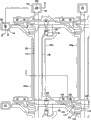
With reference to the tft array panel of Fig. 1 to Fig. 3 detailed description according to the embodiment of the invention.Fig. 1 is the layout according to the tft array panel of the embodiment of the invention, and Fig. 2 and Fig. 3 are tft array panel II-II ' along the line shown in Fig. 1 and the cutaway view of III-III '.
A plurality of gate lines 121 and a plurality of storage electrode line 131 are formed on insulated substrate 110, and this insulated substrate is by making such as the material of clear glass or plastics.Gate line 121 transmits gating signal (gate signal) and extends along horizontal direction basically.Each gate line 121 comprises a plurality of gate electrode 124 and ends 129 of stretching out (giving prominence to) downwards, and this end 129 has big area so that contact with other layer or external drive circuit.The gate driver circuit (not shown) produces gating signal and can be installed on flexible printed wiring (FPC) the film (not shown), fpc film can attached on the substrate 110, be directly installed on the substrate 110 or be attached in the substrate 110.Gate line 121 can be connected on the drive circuit, and this drive circuit can be incorporated in the substrate 110.
Give storage electrode line 131 power supplies with predetermined voltage, each storage electrode line 131 comprises and is basically parallel to main line (stem) that gate line 121 extends and many to storage electrode 133a and 133b from this main line branch.Each storage electrode line 131 is arranged between two adjacent gate lines 121, and main line is near the lower gate line in two adjacent gate lines 121.Each storage electrode 133a has anchor portion that links to each other with main line and the free end of oppositely arranging with it with 133b.The anchor portion of storage electrode 133b has big area, and its free end branch is rectilinear branches (linear branch) and branch of a curve (curved branch).Yet storage electrode line 131 can have different shape and arrange.
Gate line 121 and
storage electrode line 131 comprise
lower film 124p, 131p, 133ap and 133bp (comprising containing the Al metal, for example Al or Al alloy), and
upper membrane 124q, 131q, 133aq, 133bq (comprising containing the Mo metal, for example Mo or Mo alloy).Al-Nd (Nd being added among the Al with scheduled volume) can be as containing the Al metal.The thickness of
lower film 124p, 131p, 133ap, 133bp can be for about
Extremely
And the thickness of
upper membrane 124q, 131q, 133aq, 133bq can be for about
Extremely
In Fig. 2 and Fig. 3, for grid 124 and storage electrode line 131, its underpart film and upper membrane are indicated with diacritic p and q respectively.The side of gate line 121 and storage electrode line 131 is with respect to the surface tilt of substrate 110, and its inclination angle is in the scope of about 30~80 degree.Preferably by silicon nitride (SiN
x) or silica (Sio
X) gate insulator 140 made forms on gate line 121 and storage electrode line 131. preferably on gate insulator 140, forming by amorphous silicon hydride (be abbreviated as " a-Si) or a plurality of semiconductor band (stripe) 151 of polysilicon preparation. each semiconductor band 151 extends longitudinally substantially; and comprise that a plurality of protuberance 154. semiconductor bands 151 that expand towards gate electrode 124 are broadening at close gate line 121 and storage electrode line 131 places, so that the very large tracts of land of semiconductor band 151 covering gate polar curves 121 and storage electrode line 131.
A plurality of ohmic contact bands (stripe, band) and island (island) 161 and 165 form on transistor 151.Preferably by the heavily doped n+ hydrogenation a-Si preparation that n type impurity (for example phosphorus P) is arranged, perhaps they can be prepared by silicide for ohmic contact band and island 161 and 165.Each ohmic contact band 161 comprises a plurality of protuberances 163, and this protuberance 163 and ohmic contact island 165 are positioned on the protuberance 154 of semiconductor band 151 in couples.The side of semiconductor band 151 and ohmic contact 161 and 165 is with respect to the surface tilt of substrate 110, and its inclination angle is preferably in the scope of 30~80 degree.
A plurality of data wires 171 and a plurality of drain electrode 175 ohmic contact 161 and 165 and gate insulator 140 on form.Data wire 171 data signal, and extend longitudinally substantially to intersect with gate line 121.Each data wire 171 also intersects with storage electrode line 131, and extends between adjacent storage electrode is to 133a and 133b.Each data wire 171 comprises a plurality of to source electrode 173 and end 179 that gate electrode 124 stretches out, and this end 179 has large tracts of land and is used for contacting with other layer or external drive circuit.The data drive circuit (not shown) that is used to produce data-signal can be installed in the fpc film (not shown), FPC can attached on the substrate 110, be directly installed on the substrate 110 or be attached in the substrate 110.Data wire 171 can extend to be connected to drive circuit, and this drive circuit can be incorporated in the substrate 110.
Drain electrode 175 separates with data wire 171, and is arranged on the opposite of source electrode 173 about gate electrode 124.Each drain electrode 175 comprises wide end and narrow end.Wide end covers on the storage electrode line 131, and narrow end sections ground is surrounded by source electrode 173.
Gate electrode 124, source electrode 173 and drain electrode 175 constitute TFT together with the protuberance 154 of semiconductor band 151, have passage in the protuberance 154 of TFT between source electrode 173 and drain electrode 175.
Data wire 171 and drain electrode 175 have three-decker, comprise lower film 171p and 175p, intermediate coat 171q and 175q and upper membrane 171r and 175r. Lower film 171p and 175p are preferably made by the Mo metal (for example MoN, MoNb, MoV, MoTi and MoW) that contains of Mo or Mo alloy, intermediate coat 171q and 175q are preferably by low resistivity metal Al or contain Al metal (for example AlNd) and make, and upper membrane 171r and 175r make by having with the Mo of ITO or IZO excellent contact characteristic or the Mo metal (for example MoN, MoNb, MoV, MoTi and MoW) that contains of Mo alloy.
In Fig. 2 and Fig. 3, lower film, intermediate coat and the upper membrane of source electrode 173 and end 179 are represented with diacritic p, q and r respectively.Data wire 171 and drain electrode 175 have the edge contour of about 30~80 degree angles.
Between only underlaid semiconductor band 151 of ohmic contact 161 and 165 and the top conductor 171 and 175, so that reduce contact resistance between them.
Except the protuberance 154 that is formed with TFT on it, semiconductor band 151 has and data wire 171 and drain electrode 175 and following ohmic contact 161 and 165 flat shape much at one.Promptly, semiconductor band 151 is formed under data wire 171 and drain electrode 175 and the following ohmic contact 161,163 and 165, and comprise that some are not by the expose portion of data wire 171 and drain electrode 175 coverings, for example part between source electrode 173 and drain electrode 175.
Passivation layer 180 is formed on data wire 171, drain electrode 175, and on the expose portion of semiconductor band 151. passivation layer 180 can be by inorganic insulator (for example silicon nitride and silica), organic insulator, or low dielectric insulator is made, it can have smooth upper surface. and organic insulator and low dielectric insulator can have and be lower than about 4.0 dielectric constant. and the example of low dielectric insulator comprises that the a-Si:C:O and the a-Si:O:F. organic insulator that form by plasma enhanced chemical vapor deposition (PECVD) can present light sensitivity. and passivation layer 180 can comprise the lower film of inorganic insulator and the upper membrane of organic insulator, so that it presents the insulation property of the excellence of organic insulator, prevent that simultaneously the expose portion of semiconductor band 151 from being damaged by organic insulator.
Passivation layer 180 has a plurality of contact holes 182 and 185, and it exposes the end 179 of data wire 171 and drain electrode 175 respectively.Passivation layer 180 and gate insulator 140 have a plurality of contact holes 181 and a plurality of contact hole 184, contact hole 181 exposes the end 129 of gate line 121, and contact hole 184 exposes the part near the free end of the part of the anchor portion of storage electrode 133a and 133b or storage electrode line 131.
A plurality of pixel electrodes 191, a plurality of jumper (overpass) 84 and a plurality of contact auxiliary member (contact assistant) 81 and 82 form on passivation layer 180.They are preferably made by transparent conductor (for example ITO or IZO) or reflection conductor (for example Ag, Al or its alloy).By contact hole 185 with pixel electrode 191 physical connections and be electrically connected to drain electrode 175 so that the data voltage that receives from drain electrode 175 of pixel electrode 191.The pixel electrode 191 that is supplied with data voltage cooperates the generation electric field with the common electrode of the display pannel (not shown) staggered relatively that is supplied with common voltage.This voltage decision is placed on the direction of the liquid crystal molecule (not shown) of two liquid crystal layer (not shown) between the electrode.Pixel electrode 191 and common electrode form electric capacity (device), are called " liquid crystal capacitance (device) ", and it closes the voltage that the back storage applies at TFT.
Pixel electrode 191 covers the storage electrode line 131 that comprises storage electrode 133a and 133b.Pixel electrode 191, the drain electrode 175 that is connected thereto and storage electrode line 131 form building-out condenser, are called " holding capacitor ", and it has strengthened the charge storage of liquid crystal capacitance.
Contact auxiliary member 81 and 82 is connected to the end 129 of gate line 121 and the end 179 of data wire 171 respectively by contact hole 181 and 182.Contact auxiliary member 81 and 82 protection ends 129 and 179, and the adhesive force between enhancing end and the external equipment.
Jumper 84 is crossed over gate lines 121, and is connected respectively to by a pair of contact hole 184 on the exposed end of the expose portion of storage electrode line 131 and storage electrode 133b free end, and this is provided with about gate line 121 relative to one another to contact hole.The storage electrode line 131 that comprises storage electrode 133a and 133b can be used to repair defective on gate line 121, data wire 171 or TFT with jumper 84.
To describe the manufacture method that is shown in the tft array panel among Fig. 1 to Fig. 3 in detail with reference to figure 4 to Figure 20 and Fig. 1 to Fig. 3 according to the embodiment of the invention., the lower film of AlNd and the upper membrane that contains the Mo metal are deposited in order on the insulated substrate 110 to shown in Figure 6 as Fig. 4, insulated substrate 110 is by making such as the material of clear glass or plastics.
Then, by wet etching upper membrane and lower film, formation comprises a plurality of gate lines 121 of gate electrode 124 and end 129 and the storage electrode line 131 that comprises storage electrode 133a and 133b.
As shown in Figure 7 and Figure 8, will be deposited on successively on gate line 121 and the storage electrode line 131 by the PECVD method by the gate insulator of making such as the material of SiNx 140, intrinsic (pure) a-Si layer 150 and extrinsic (impure) a-Si layer 160.Intrinsic a-Si layer 150 is made by amorphous silicon hydride, and extrinsic a-Si layer 160 is by the heavily doped n+ hydrogenation a-Si preparation that has such as the n type impurity of phosphorus P.
Sequentially, will by contain the metal bottom of Mo Mo film 170p, by containing middle Al film 170q that the Al film makes and by containing top Mo film 170r that the Mo film makes by the sputter sequential aggradation, thereby form data metal layer 170.
Photoresist is coated on the Mo film 170r of top. by the exposed mask (not shown) with resist exposure, and as shown in Figures 9 and 10, the photoresist that develops has the thickness that depends on the position. and the photoresist of development comprises that a plurality of first is positioned at passage area B to third part 54 and 52. firsts 54, and second portion 52 is positioned at data wire zone A. and not have to give the third part sign that is positioned at reserve area C drawing reference numeral, because their thickness is zero substantially. according to the processing conditions of subsequent process steps, regulate the thickness ratio of first 54 and second portion 52. the thickness of preferred first 54 is equal to or less than half of thickness of second portion 52.
Can obtain the thickness that depends on the position of photoresist by some technology, for example, by being provided at translucent area and transparent region and the light blocking zone of opacity on the exposed mask.The film that translucent area can have slit-type pattern, grid type pattern, have medium transmissivity or intermediate gauge.When using the slit-type pattern, the width of preferred slit or the distance between the slit are less than the resolution of the light projector that is used for photoetching.Another embodiment uses (reflowable) photoresist that can reflux.In detail, by using the common exposed mask only have transparent region and zone of opacity, in case but forming the photoresist pattern of making by reflow materials, reflux course just takes place flowing to the zone that does not have photoresist in it, thereby forms thin part.
With reference to Figure 11 and 12, adopt wet etch method the part 174 and 179 of data metal layer 170 to be left on data area A and the passage area B in the expose portion etching of the data metal layer on the reserve area C 170.Then, by dry ecthing method will be on reserve area C the expose portion of extrinsic a-Si layer 160 and the underclad portion of intrinsic semiconductor layer 150 remove, make to form semiconductor pattern 161,164,151 and 154.
Then, by etch back process (etch back process) the photoresist pattern 54 on the passage area B is removed.Simultaneously, the thickness with photoresist pattern 52 reduces scheduled volume.
With reference to Figure 13 and Figure 14, adopt photoresist pattern 52 as mask, with data metal patterns 174 wet etchings that expose, so that data metal patterns 174 is divided into source electrode 173 and drain electrode 175, and the extrinsic semiconductor pattern on the passage area between source electrode 173 and the drain electrode 175 164 that makes exposes.
Adopt photoresist pattern 52 as mask, with extrinsic semiconductor pattern 164 dry ecthings on the passage area.At this moment, chlorine-containing gas or fluoro-gas are used for dry ecthing.Chlorine-containing gas can be for containing the gas of chlorine atom, for example Cl
2, HCl, BCl
3, CCl
4, or SiCl
2H
2The fluoro-gas of scheduled volume can be supplied so that improve the performance of the intrinsic semiconductor 154 of lower floor, and fluorine atom (SF for example can be comprised
6Or CF
4).Can be in company with the chlorine-containing gas that is used for dry ecthing and fluoro-gas supplying inert gas, for example H together
2And He.Dry ecthing is to carry out under the pressure of about 100mT to 800mT.
When chlorine-containing gas is HCl, for example, use HCl+SF
6+ He is during as etching gas, preferably about 1: 4 to 1: 10 of the flow-rate ratio of fluoro-gas and HCl gas.When chlorine-containing gas is Cl
2The time, for example, use Cl
2+ SF
6+ He is during as etching gas, fluoro-gas and Cl
2Preferably about 1: 1 to 1: 10 of the flow-rate ratio of gas.Flow-rate ratio has the scope that can improve the TFT performance but not influence dry ecthing.Especially, because Cl
2Atomic group (radical) or emission of ions take place less than the bond dissociation energy of HCl in bond dissociation energy easily that have, make the gas consumption of dry ecthing reduce.Chlorine-containing gas has improved the performance of TFT.
In detail, when using identical photoresist pattern etching data metal patterns 171,174 and 179 and during intrinsic semiconductor 150, the data wire 171 that comprises source electrode 173 and end 179 with comprise that the semiconductor 151 of protuberance 154 has essentially identical flat shape.The zone that semiconductor 151 is exposed to from the light of light source (for example back lighting device) broadens, and has improved light leakage current (photo leakage current).The light leakage current appreciable impact has the data wire 171 of the sandwich construction of Al film and the Mo of lower floor film.That is, in wet etching, Mo is diffused into semiconductor 151, decomposes the contaminating impurity channel semiconductor that (split, separation) comes out from following Al film.Therefore, reduced the TFT characteristic of cut-off current (off-current), threshold voltage, after image has taken place.
Yet, when etching extrinsic semiconductor pattern 164, promptly, when forming passage area, with the flow-ratio control of chlorine-containing gas and fluoro-gas in predetermined ratio, so that reduce above-mentioned shortcoming. when forming passage area, when the chlorine-containing gas that uses in this scope, remaining Cl atom remains in the protuberance 154 of semiconductor 151.
Table 1 illustrates test case, and it shows when forming passage area, when the flow of the flow of chlorine-containing gas and fluoro-gas not simultaneously, the after image minimizing.In each test examples, pressure, power and He supply are respectively 170mT, 3400W and 900sccm.In addition, in each test examples, SF
6Flow set be 150sccm, based on the flow of SF6 from about 0 to predetermined ratio control Cl
2Or the flow of HCl, so that suitable flow to be provided.
The after image characteristic test is as follows.At first, the preparation display pannel that is used to test, it comprises by having the passage area that the etching gas of corresponding discharge ratio separately forms.Each display pannel all comprises a plurality of pixels that are arranged as matrix thereon.To represent one of them data voltage of middle gray (intermediate gray) between lime (whitegray) and grey black (black gray) to be applied to display pannel, so that measure the brightness of the display screen of display pannel respectively.Then, will alternately apply horizontal and vertical, to show ash and lime about ten hours corresponding to the data voltage of grey black and lime.Then, after the data voltage that applies again corresponding to middle gray, detect the brightness of display screen, to measure after image degree (afterimage degree).
Table 1
| Flow-rate ratio (SF
6∶Cl
2)
|
After image improves |
Etching characteristic |
Flow-rate ratio (SF
6∶HCl)
|
After image improves |
Etching characteristic |
| 1∶0 |
× |
◎ |
1∶0 |
× |
◎ |
| 1∶0.3 |
× |
◎ |
1∶1.12 |
× |
◎ |
| 1∶0.7 |
△ |
◎ |
1∶3 |
× |
◎ |
| 1∶1 |
○ |
◎ |
1∶3.5 |
△ |
◎ |
| 1∶4 |
○ |
◎ |
1∶4 |
○ |
◎ |
| 1∶6 |
◎ |
◎ |
1∶6.5 |
○ |
◎ |
| 1∶8.2 |
◎ |
◎ |
1∶9 |
◎ |
◎ |
| 1∶9.4 |
◎ |
○ |
1∶9.5 |
◎ |
○ |
| 1∶10 |
◎ |
○ |
1∶10 |
◎ |
○ |
| 1∶11.2 |
◎ |
△ |
1∶11.2 |
◎ |
△ |
| 1∶13 |
◎ |
△ |
1∶13 |
◎ |
△ |
◎: excellent/zero: good/△: general/*: poor
As shown in table 1, work as SF
6: Cl
2Or SF
6: the flow-rate ratio of HCl was respectively 1: 1 or is higher, perhaps 1: 4 or when higher, had significantly improved after image.Owing to compare Cl with HCl
2Bond dissociation energy less, make emission atomic group or ion easily, Cl
2Flow-rate ratio less than the flow-rate ratio of HCl.Yet, work as SF
6: Cl
2Or SF
6: the flow-rate ratio of HCl was greater than 1: 10 o'clock, and etching characteristic is affected.
According to the analysis result that uses secondary ion mass spectrometry (SIMS) (SIMS) method, the amount that records the Cl atom that remains on the semi-conductive passage area is about 3.0% to 20% (atom number).
Figure 21 a and Figure 21 b are shown specifically the curve chart of the performance of TFT with the variation of Cl supply.Figure 21 a works as SF for illustrating
6: the flow-rate ratio of HCl is 390sccm: 470sccm, promptly 1: 1 o'clock, and leakage current I
dWith grid voltage V
gVariation, Figure 21 b illustrates and works as SF
6: the flow-rate ratio of HCl is 150sccm: 750sccm, promptly 1: 5 o'clock, and leakage current I
dWith grid voltage V
gVariation.In the darkroom, measure leakage current I with the curve representative that label A indicates
dSituation, and leakage current I is measured in the curve of indicating with label B representative in light-struck bright chamber
dSituation.
Shown in curve chart, the light leakage current among Figure 21 a is greater than the light leakage current among Figure 21 b.Light leakage current comprises the voltage drop of drain voltage, to produce after image.With reference to Figure 15 to Figure 17, remaining photoresist pattern 52 is removed again.To shown in Figure 20, passivation layer 180 forms on the protuberance 154 of the exposure of the gate insulator 140, data wire 171 and the drain electrode 175 that expose and semiconductor 151 as Figure 18.
Then, passivation layer 180 is removed, so that form a plurality of contact holes 181,182,184 and 185 by photoetch.At last, as shown in Figure 1 to Figure 3,, on passivation layer 180, form transparent conductive material (for example ITO or IZO), and make its one patterned, to form pixel electrode 191, contact auxiliary member (contact assistant) 81 and 82 and jumper 84 by sputter.
According to the present invention, data wire is formed by the sandwich construction that comprises Al film and Mo film, and uses the etching gas of predetermined amount of flow ratio to form passage area.Thereby, improved the performance of TFT, and reduced the generation of after image.
Although described the present invention in conjunction with the exemplary embodiment that is considered to put into practice; but should be appreciated that; for those skilled in the art, various changes and equivalent arrangements will obviously also can be implemented, and do not deviate from spirit of the present invention and protection range.