CN1723552A - Reduced splattering of unpassivated laser fuses - Google Patents
Reduced splattering of unpassivated laser fuses Download PDFInfo
- Publication number
- CN1723552A CN1723552A CNA038222558A CN03822255A CN1723552A CN 1723552 A CN1723552 A CN 1723552A CN A038222558 A CNA038222558 A CN A038222558A CN 03822255 A CN03822255 A CN 03822255A CN 1723552 A CN1723552 A CN 1723552A
- Authority
- CN
- China
- Prior art keywords
- fusable link
- blast barrier
- fuse
- metal wire
- laser
- Prior art date
- Legal status (The legal status is an assumption and is not a legal conclusion. Google has not performed a legal analysis and makes no representation as to the accuracy of the status listed.)
- Granted
Links
Images


Classifications
-
- H—ELECTRICITY
- H01—ELECTRIC ELEMENTS
- H01L—SEMICONDUCTOR DEVICES NOT COVERED BY CLASS H10
- H01L27/00—Devices consisting of a plurality of semiconductor or other solid-state components formed in or on a common substrate
- H01L27/02—Devices consisting of a plurality of semiconductor or other solid-state components formed in or on a common substrate including semiconductor components specially adapted for rectifying, oscillating, amplifying or switching and having at least one potential-jump barrier or surface barrier; including integrated passive circuit elements with at least one potential-jump barrier or surface barrier
-
- H—ELECTRICITY
- H01—ELECTRIC ELEMENTS
- H01L—SEMICONDUCTOR DEVICES NOT COVERED BY CLASS H10
- H01L23/00—Details of semiconductor or other solid state devices
- H01L23/52—Arrangements for conducting electric current within the device in operation from one component to another, i.e. interconnections, e.g. wires, lead frames
- H01L23/522—Arrangements for conducting electric current within the device in operation from one component to another, i.e. interconnections, e.g. wires, lead frames including external interconnections consisting of a multilayer structure of conductive and insulating layers inseparably formed on the semiconductor body
- H01L23/525—Arrangements for conducting electric current within the device in operation from one component to another, i.e. interconnections, e.g. wires, lead frames including external interconnections consisting of a multilayer structure of conductive and insulating layers inseparably formed on the semiconductor body with adaptable interconnections
- H01L23/5256—Arrangements for conducting electric current within the device in operation from one component to another, i.e. interconnections, e.g. wires, lead frames including external interconnections consisting of a multilayer structure of conductive and insulating layers inseparably formed on the semiconductor body with adaptable interconnections comprising fuses, i.e. connections having their state changed from conductive to non-conductive
- H01L23/5258—Arrangements for conducting electric current within the device in operation from one component to another, i.e. interconnections, e.g. wires, lead frames including external interconnections consisting of a multilayer structure of conductive and insulating layers inseparably formed on the semiconductor body with adaptable interconnections comprising fuses, i.e. connections having their state changed from conductive to non-conductive the change of state resulting from the use of an external beam, e.g. laser beam or ion beam
-
- H—ELECTRICITY
- H01—ELECTRIC ELEMENTS
- H01L—SEMICONDUCTOR DEVICES NOT COVERED BY CLASS H10
- H01L2924/00—Indexing scheme for arrangements or methods for connecting or disconnecting semiconductor or solid-state bodies as covered by H01L24/00
- H01L2924/0001—Technical content checked by a classifier
- H01L2924/0002—Not covered by any one of groups H01L24/00, H01L24/00 and H01L2224/00
Abstract
The act of blowing an unpassivated electrical fuse (for example, fuse 405) using a laser can result in the splattering of the fuse material and result in electrical short circuits. A blast barrier (for example blast barrier 406) formed around an area of the fuse that is blown by the laser helps to contain the splattering of the fuse material. The blast barrier may be formed from the same material as the fuses themselves and therefore, can be created in the same fabrication step.
Description
Technical field
Present invention relates in general to the manufacturing of integrated circuit, especially prevent to produce short circuit in the laser fuse that splashes in other of fuse materials when the non-passivation laser fuse blows.
Background technology
In the manufacturing of integrated circuit, had for a long time and used laser fuse.A kind of application of laser fuse is the intended purpose according to integrated circuit, the specific function in activation or the inactive integrated circuit.For example, can carry out single design, make it to have complete function set integrated circuit.But, depend on the price when integrated circuit is sold, can forbid specific function.In another kind was used, laser fuse allowed to replace defective device and circuit in the integrated circuit with the standby device and the circuit of operate as normal.Generally, when integrated circuit being tested when verifying its service behaviour, testing equipment is carried out mark (perhaps storing) to the defective part of integrated circuit.Subsequently, carry out an independent operation, specific laser fuse is blown,, replace it with device and the circuit that can work to remove defective device and circuit.
As its name suggests, use the high energy laser that effectively melts and evaporate subsequently the connection of fusible to blow laser fuse.When fusable link fused, the fuse materials of evaporation might be splashed to adjacent fuse uncontrollably.The fuse materials of splashing and then may cause adjacent fuse work incorrect, the fuse that just causes before having been fused show as the fuse of fusing not, perhaps make the adjacent fuse that has fused short circuit together.If this thing happens, then integrated circuit can not normally be worked.
Laser fuse has two kinds of principal modes, the non-passivation of passivation.Passivated laser fuse has a passivation layer at the top, be not subjected to the infringement of operational environment with the protection laser fuse.For the fusable link of making such as copper (Cu) with corrosion-prone material, the use of passivation layer is even more important.The non-passivation laser fuse does not have passivation layer, is subjected to the infringement of disagreeableness environment easily.Because the non-passivation laser fuse is open to environment, tend to make the non-passivation laser fuse such as aluminium (Al) with anticorrosive (perhaps erosion-resisting comparatively speaking) material.Passivated laser fuse is very insensitive to splashing of vaporized fuse material, and this is because passivation layer provides protection.On the other hand, passivation layer makes laser fuse more be difficult to fusing.This is owing to be used for the laser of blow out fuse and must have enough energy and can penetrate passivation layer before the vaporized fuse material, sets up enough big pressure and the passivation layer at fusable link top is broken and discharges evaporating materials.
On the other hand, passivation makes it possible to fuse safely laser fuse, can not influence adjacent circuit.This be because, the molten material that passivation layer has prevented fusable link immediately, fierce release.Sometimes, in the fuse failure process, after fusable link was by laser fusing at first, fusable link had absorbed abundant energy, makes heated fusable link be evaporated.Materials evaporated produces a pressure, and this pressure certainly will make its lapping break at the most fragile point of material.Most fragile point generally is the passivation layer that covers.When being deposited on the chip surface again, deposit is extremely thin non-conductive film from the described evaporating materials produced of breaking itself.
Using mechanical stability low, in the integrated circuit such as the made of low K dielectrics, breaking that the release of vaporized fuse material causes may not only appear in the passivation layer, and can appear in the dielectric layer that underlies.This can cause serious damage to circuit, if especially the material to corrosion-susceptible is used for plain conductor such as copper.In this case, the non-passivation fuse is set on such integrated circuit, to reduce the impaired chance in surface that in the fuse failure process, underlies.In order to provide extra safeguard measure to the surface of underliing, can and underlie at fuse layer (fuse level) is provided with a hard dielectric layer between the surface.Unfortunately, if there is not passivation layer, the fuse failure process can be subjected to the influence of following aspect: the fuse materials of fusing may not evaporated when having enough heats, and this has stoped molten metal all to evaporate.The evaporation of the part of deposite metal may cause still remaining the splashing of fuse materials of liquid form.The fuse materials of splashing may cause the electrical short of the non-passivation fuse adjacent with the fuse that is fusing.Splash effect depends on many parameters, such as the power and the wavelength of laser, the size of fusable link, the material of fuse etc.
United States Patent (USP) 6,160,302 have proposed to form wall between laser fuse, with the adjacent fuse of fuse that prevents that unexpected fusing of out-of-alignment laser and laser from will fuse.
United States Patent (USP) 6,300,232 have proposed to set up around single laser fuse and have stopped, with the physically impaired expansion that prevents that laser produces in the fuse failure step thermal conductance from causing.
United States Patent (USP) 5,899,736 propose partly to surround individual electric fusable link with dielectric barrier, with selecting of the fuse materials that prevents to spray.
Therefore, need a kind of method, the laser fuse contiguous to the laser fuse that fused provides protection, but can significantly not increase cost aspect additional space demand and/or the extra manufacturing step.
Summary of the invention
In one aspect, the invention provides a kind of semiconductor device, it comprises first electrical contact pad, second electrical contact pad and the fusable link of being made by electric conducting material, this fusable link has the first end that is connected to first electrical contact pad and is connected to the second end of second electrical contact pad, this fusable link will become nonconducting after applying an energy source, flatly surround a blast barrier of described fusable link, in order to hold owing to applying the fusable link material that described energy source penetrates.
On the other hand, the invention provides a kind of method of semiconductor device being set up blast barrier, comprise the steps: to form first and second electrical contact pad, formation is connected to the fusable link of first and second electrical contact pad, and formation conduction blast barrier, this blast barrier has and is parallel to first parts that described fusable link forms, and be parallel to that described fusable link forms, at second parts of the side opposite of fusable link with described first parts.
Aspect another, the invention provides a kind of structure, it comprises first and second pads, be formed on first metal wire between first and second pads, this first metal wire contacts first and second pads, with the second and the 3rd metal wire of the relative both sides that are formed on first metal wire, the second and the 3rd metal wire separates a blank that equals to set a distance with described first metal wire.
In a word, the invention provides a kind of salvo of the fuse materials of splashing of the integrality that may damage adjacent fuse at the non-passivation laser fuse.The present invention just revises the concrete layout of the metal level that forms fusable link without any need for extra treatment step.By using the metal wire that extends in the fusable link both sides, the invention provides protection at the material that splashes.Described metal wire can be connected to the through hole of the electrical connection that is established to other circuit,, the length of metal wire and other physical characteristic (such as thickness and width) guarantee after the fusing process that fuse has taken place that being connected between the through hole of the fusable link that is fused to have electrical connection but should being set to.Described metal wire is as the mechanical stop body at the deposite metal of splashing in the fuse failure process.
The present invention has many advantages.For example, use the preferred embodiments of the present invention, by using blast barrier, can provide the protection to the contiguous fuse of the fuse that fused, described blast barrier can be used and the identical materials manufacturing of laser fuse own.By using and the manufacturing of laser fuse identical materials, can in the manufacturing step identical, form blast barrier, thereby not need extra manufacturing step with laser fuse.Compare with other solution of the extra procedure of processing of needs, this has reduced the overall manufacturing time and the cost of the integrated circuit that comprises laser fuse.
In addition, the use of the preferred embodiments of the present invention also allows to add blast barrier and the spacing that do not change laser fuse.Therefore, the density of integrated circuit can not change.On same chip area, the laser fuse of as much can be set.
In addition, the use of the preferred embodiments of the present invention allows to add blast barrier, and this need make an amendment slightly to the manufacturing mask that produces laser fuse itself.Therefore, can easily make amendment, and need not circuit and device are carried out again Butut and setting existing design.
Description of drawings
Specification below reading in conjunction with the accompanying drawings can more be expressly understood above-mentioned feature of the present invention.In the accompanying drawing:
Fig. 1 a, 1b and 1c illustrate the vertical view and the profile of non-passivation laser fuse, and the vertical view of array of fuses;
Fig. 2 a and 2b illustrate at laser fuse 205 by the vertical view of the array of fuses before and after the laser blown;
Fig. 3 a, 3b and 3c illustrate according to a preferred embodiment of the present invention, have the vertical view and the end view of the non-passivation laser fuse of whole blast barrier, and the vertical view of array of fuses;
Fig. 4 a and 4b illustrate at laser fuse 405 by the vertical view of the array of fuses before and after the laser blown, and wherein, described integral blast barrier has prevented the effusion of the chip that the evaporation institute impelling of fuse materials goes out;
Fig. 5 illustrates the alternative of blast barrier according to a preferred embodiment of the present invention;
Fig. 6 a and 6b illustrate the alterative version of blast barrier according to a preferred embodiment of the present invention;
Fig. 7 a illustrates the alternative of fusable link according to a preferred embodiment of the present invention to 7c.
Embodiment
Describe manufacturing and the use of various embodiment below in detail.But, should be appreciated that to the invention provides many applicable inventive concepts that they can be by specific implementation in many specific context environmentals.Specific embodiment as described herein just is used for explaining manufacturing and using indivedual mode of the present invention, is not to limit the scope of the invention.
See Fig. 1 now, this figure illustrates the vertical view of the non-passivation laser fuse 100 on the hard dielectric layer 115.This hard dielectric layer is at the top of a substrate 116 (Fig. 1 a is not shown, but is present in the profile of back).As previously mentioned, the difference of non-passivation laser fuse and passivated laser fuse is that the former lacks its passivation layer not affected by environment of protection.Compare with passivated laser fuse, the required laser energy of the fusing of non-passivation laser fuse still less.This is because before laser can fuse laser fuse, laser needn't at first see through passivation layer.And then when being exposed to the absorbed laser energy of laser, more the use of high energy laser produces more substantial heat.Material for particular types, such as special low k (dielectric constant) material (for example substrate of making by the combination of organic substance and silicon), responsive comparatively speaking to heat, excessive heat in the time of generally can not bearing the fusing passivated laser fuse, described material can not bear the mechanical stress that is associated with the fusing of passivated laser fuse.In addition, the mechanical property of the material such as low-k materials may not be the pressure that vaporized fuse material produced that is well suited for bearing rapid expansion.
The vertical view of laser fuse 100 has shown three major parts of laser fuse: allow laser fuse 100 is electrically connected to two pads 105 of circuit and device, and fusable link 110.In illustrated embodiment, pad 105 is physically greater than fusable link 110.In alternative, the width of pad 105 and fusable link 110 can identical (for example, fuse looks like solid wire).Notice that although illustrated fusable link 110 is straight lines, fusable link 110 can form multiple shape, such as the line of zigzag line, curve, width and varied in thickness etc.Pad 105 is parts that the permission of line is connected to conductor wire semiconductor device.
Fusable link 110 is parts that then ruptured by LASER HEATING of laser fuse.Best, described two pads 105 and fusable link 110 are by making with a kind of electric conducting material.In fact fusable link 110 can use the metal manufacturing of any kind, but aluminium is preferable material, and this is because the fusing point of aluminium is relatively low, and activity is not high comparatively speaking.In addition, aluminium is exactly to select for use to carry out the metal that semiconductor is made for a long time.Other material that can be used for fusable link 110 comprises gold, and more inferior have copper and silver.Also can use various alloys, as long as their corrosion-vulnerable not comparatively speaking.
Present 1b with the aid of pictures, this figure illustrate the cutaway view of the laser fuse 100 on the hard dielectric layer 115 at 116 tops of the substrate shown in Fig. 1 a, and section is along the dotted line that is designated as B-B.This cutaway view illustrates two pads 105 to have and passes the conductive channel that hard dielectric layer 115 enters substrate 116 downwards, is connected to the tie point 120 that is used for circuit and device.
Present 1c with the aid of pictures, this figure illustrate the array of fuses 150 of three laser fuses arranging according to linear mode.Generally laser fuse is arranged to array, and arranges as close as possiblely, so that the surface area that they occupy in integrated circuit minimizes.Interval between the fuse is called fuse pitch, and the width that fuse pitch is defined as fuse adds two spacings between the adjacent fuse.Fuse pitch is more little, and fuse just leans on closely more.Illustrated array of fuses 150 has three laser fuses (155,160 and 165) among Fig. 1 c, but array of fuses can have the fuse sets of any amount to lump together, and is the physical size in semiconductor surface zone to the constraint of fuse quantity in the array of fuses.
Fuse can fuse in many ways.For example, electric current is exactly the another kind of mode of blow out fuse.But,, use the fuse of current fusing fusable link also to be of little use owing to the delicate nature of most devices in the integrated circuit and circuit.Also can be by fuse is exposed to radiant energy and blow out fuse.No matter when, the present invention can both be applied to be different from the fuse that the mode of using laser fuses.
Laser fuse uses LASER HEATING and evaporates its fusable link.It is the same using laser fusion to cut off fusable link then, no matter laser fuse be the passivation type or the non-passivation type.For passivated laser fuse, laser must pass through passivation layer before can evaporating fusable link.This can use the laser of specific wavelength to realize that passivation layer does not absorb the laser of this wavelength.For example, normally used passivation layer SiO
2Allow the laser energy of specific wavelength to pass through, and can significantly not absorb laser energy.So just laser energy can be concentrated and be used to the fusable link that fuses.
Present 2a with the aid of pictures, this figure illustrates an array of fuses 200, and wherein, a laser spot 220 is irradiated on the fusable link of laser fuse 205, in order to the fusing laser fuse, can be by the irradiation position of laser spot 220 be brought in the fusing laser fuse near one of fusable link comparatively speaking.This helps the fusable link at two position fusing laser fuses, and each position is near an end of fusable link.
As previously mentioned, the described fusable link that fuses of the heat effect by laser spot 220.At first, the fuse materials of fusable link is melted, then evaporation.The duration of fusing and evaporation process is extremely of short duration, to prevent the excessive buildup of heat.Basically, fusing process just is through with before heat permeates into zone outside the fuse join domain.Therefore, the fusing of fuse materials and evaporation usually are similar to blast: in fact the fuse materials of being shone by laser spot 220 is exploded and is come.
As previously mentioned, if laser fuse is the passivated laser fuse type, then the chip of blast generation does not probably cause any problem, and this has two possible reasons: first reason is that passivation layer provides effective protection, because it has covered the surface of adjacent fuse; Second reason is the bottled up fuse materials of fusing of passivation layer, evaporates fully up to it, and the chip that the fuse materials of evaporation produces is non-conductive often, because it has been distributed on the very big zone.But for the non-passivation laser fuse, the fuse materials of fusing is unfettered, may just be penetrated under molten state.If fuse materials is penetrated under molten state, its degree of scatter is not enough so that it is non-conductive.Therefore, chip may cause short circuit.Depend on where chip drops on, the laser fuse of the close fuse that is fused may be to himself causing short circuit (problem that has occurred) when adjacent fuse has been fused before this, and perhaps adjacent laser fuse may mutual electrical short.
Present 2b with the aid of pictures, this figure illustrate an array of fuses 250, and wherein first laser fuse 205 is by laser blown, and the chip (for example fragment of fuse materials 255) that this fusing operation produces makes laser fuse 210 and first laser fuse, 205 electrical shorts.For example, the fuse materials fragment 255 that penetrates from the fuse materials of the fusing of the fusable link of first laser fuse 205 has formed an electric bridge between first laser fuse 205 and adjacent laser fuse 210, with two laser fuse short circuits together.Because the different circuit of each laser fuse tie point comprises by the very possible cisco unity malfunction of the integrated circuit of the laser fuse of short circuit, therefore to go out of use.
Present 3a with the aid of pictures, according to a preferred embodiment of the present invention, this figure illustrates at substrate 321 (invisible among Fig. 3 a, but in the end view of back, illustrate) the hard dielectric layer 320 at top on the vertical view of laser fuse 300, wherein, laser fuse 300 has built-in blast barrier 315, helps prevent the sputter of melting fuse materials to produce the electric bridge of adjacent laser fuse.Described blast shield is formed on each side of fusable link 310, and is formed on each end in fusable link 310, forms will be surrounded by the level in the zone of laser burn around fusable link 310.Notice that as previously mentioned, although fusable link 310 is illustrated as straight line, it can adopt other form, such as the line of zigzag, curve, variable-width etc.According to a preferred embodiment of the present invention, blast barrier 315 is by forming with the identical materials of laser fuse own.Therefore, blast barrier 315 can be set up in the manufacturing step identical with laser fuse, thereby does not need extra manufacturing step.But, also can form described blast shield 315 with the material of any other type compatible with the manufacturing of integrated circuit, comprise with non-conducting material and making.
According to a preferred embodiment of the present invention, because blast barrier 315 usefulness and laser fuse identical materials or make, must not can be in contact with one another in the blast barrier 315 of each end of single laser fuse by any electric conducting material.If they are in contact with one another, then clean effect is exactly to have produced a conduction that walks abreast with described fusable link to be connected.If blast barrier 315 usefulness non-conducting materials form, then the blast barrier 315 of single laser fuse can be allowed to be in contact with one another.In addition, because the cause of through hole, raceway groove and the further feature that can form below laser fuse in substrate may not form along the blast barrier of the whole length of fusable link.
Present 3b with the aid of pictures and 3c, they illustrate the end view (visual angle is about 45 degree above horizontal plane) of the laser fuse 300 that has blast barrier 315, and the vertical view that the array of fuses 350 of three laser fuses 355,360 and 365 is arranged.According to a preferred embodiment of the present invention, because blast barrier forms in the same manufacturing step that forms laser fuse, the height of blast barrier can be substantially equal to the height of laser fuse itself.But if blast barrier forms with different manufacturing steps, then the height of blast barrier can be set to make the height of its maximum effect.This means and blast barrier can be formed the height the same, perhaps can be higher than laser fuse with laser fuse.Notice that because the design of blast barrier, the fuse pitch of array 350 does not have to change (comparing with the array of fuses 150 that Fig. 1 c shows).Therefore, the constructed in accordance laser fuse similar with the quantity of not protected laser fuse can be set.
Present 4a with the aid of pictures, this figure illustrates an array of fuses 400 according to a preferred embodiment of the present invention, and it is made of the fuse with blast barrier, wherein, on the fusable link of laser fuse 405, shone a laser spot 420, to blow fusable link.Are blast barrier 406 tightly around the fusable link of laser fuse 405.Notice that in full force and effect in order to make blast barrier, blast barrier 406 should extend beyond the zone that fusable link will be evaporated by laser spot 420.If blast barrier 406 does not extend beyond the zone that fusable link will be evaporated, then the effect of blast barrier can be detracted, and the vaporized fuse material of being blocked by blast barrier may not form electrical short with other laser fuse.
Present 4b with the aid of pictures, this figure illustrates array of fuses 450 according to a preferred embodiment of the present invention, wherein first laser fuse 405 is by laser blown, and the chip (for example the fuse materials fragment 455) that fusing operation produces is centered on the blast barrier of first laser fuse 405 and blocks.Laser, for example (Fig. 4 a) generally can be splashed to uncertain distance in uncertain mode to the chip 455 that the evaporation of fuse materials forms to laser spot 420, then is constrained in the present embodiment near the blast barrier 406 that forms the position that first laser fuse 405 will be fused.The sealing that blast barrier 406 forms around blast area encases the vaporized fuse material that penetrates in the fuse failure process.
According to a preferred embodiment of the present invention, blast barrier can form in forming the same manufacturing step of laser fuse, and uses with the fuse identical materials and form.Perhaps, blast barrier can be made with any material compatible with the manufacturing process of making integrated circuit.If use extra manufacturing step to form described blast barrier, then described blast fuse is preferably made by non electrically conductive material.
See Fig. 5 now, this figure illustrates according to a preferred embodiment of the present invention, has the laser fuse 500 of L shaped blast barrier.Described blast barrier 515 is formed L shaped, and this L shaped long part and short vertical component of extending out from pad forms a more complete sealing to the part that will fuse of fusable link 510.Note,, then should not allow its to contact fusable link 510, unless at one end (such as passing through pad 505) if blast barrier 515 is formed by electric conducting material (such as fuse materials itself).Perhaps, blast barrier can form same effectively other shape aspect the part that will fuse of complete closed fusable link.
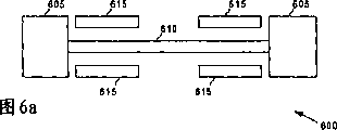
Present 6a with the aid of pictures and 6b wherein illustrate the alternative embodiment of the laser fuse that has blast barrier according to a preferred embodiment of the present invention.In Fig. 6 a, illustrate the laser fuse 600 that has blast barrier, this blast barrier 615 is not conductively coupled to pad 605 or fusable link 610, blast barrier 615 self does not have electric coupling (just yet, the part of an end that centers on laser fuse 600 of blast barrier, and the part around the other end of blast barrier, do not couple mutually).And in Fig. 6 b, the blast barrier 665 of illustrated laser fuse 650 not with pad 655 or fusable link 660 electric couplings, but blast barrier 665 forms single part, the protection fusable link 660 whole length.
Present 7a with the aid of pictures is to 7c, and picture in picture has shown the alternative of fusable link according to a preferred embodiment of the invention.In Fig. 7 a, illustrate the fusable link 710 of zigzag shape, and in Fig. 7 b, illustrate the fusable link 720 of curve shape.At last, in Fig. 7 c, illustrate the linear fusable link 730 of change width.The structure of fusable link can also have other embodiment, the be tied domination of condition of its net shape, and described constraints is such as being the maximum current flow of desirable resistivity, carrying, the configuration of the substrate that underlies etc.
According to another kind of preferred embodiment of the present invention, the height of blast barrier equals the height of laser fuse.But the height of blast barrier can change, and makes it highly can be greater than or less than the height of laser fuse, so that more effectively surround the explosive material of evaporation.
Although invention has been described in conjunction with illustrative embodiment above, on state should not be interpreted as restrictive.Various variations and the combination of above-mentioned illustrative embodiment, and other embodiments of the invention, it all is conspicuous coming institute for the those of ordinary skills that read this specification.Therefore, the scope of appended claim can not any such modification or embodiment.
Claims (26)
1. semiconductor device comprises:
First electrical contact pad;
Second electrical contact pad;
By the fusable link that electric conducting material is made, this fusable link has the first end that is connected to first electrical contact pad and is connected to the second end of second electrical contact pad, and this fusable link will become nonconducting after applying an energy source; And
Flatly surround the blast barrier of described fusable link, in order to hold owing to applying the fusable link material that described energy source penetrates.
2. semiconductor device as claimed in claim 1, wherein, described blast barrier, described fusable link and described first and second electrical contact pad are made by same material, and make in same manufacturing step.
3. semiconductor device as claimed in claim 2, wherein, described blast barrier is separated with the described first and second electrical contact pad electricity.
4. semiconductor device as claimed in claim 2, wherein, described blast barrier is separated with described fusable link electricity.
5. semiconductor device as claimed in claim 2, wherein, described blast barrier is formed the physical height that is higher than the fusable link and first and second electrical contact pad.
6. semiconductor device as claimed in claim 1, wherein, described blast barrier comprises two parts, wherein first parts are positioned near the side of described fusable link, be orientated parallel with described fusable link, second parts of blast barrier are positioned near the side opposite with described first parts of described fusable link, are orientated parallel with described fusable link.
7. semiconductor device as claimed in claim 6, wherein, two parts of described blast barrier are shaped as similar line segment shape.
8. semiconductor device as claimed in claim 6, wherein, described blast barrier has two, wherein first blast barrier is connected to described first electrical contact pad, second blast barrier is connected to described second electrical contact pad, wherein, described first and second blast barrier electricity separation mutually.
9. semiconductor device as claimed in claim 6, wherein, described fusable link is exposed under the laser so that described fusable link disconnects, and described blast barrier surrounds described fusable link in the position that described fusable link is exposed to laser in the horizontal direction.
10. semiconductor device as claimed in claim 1, wherein, described fusable link is made by having low-melting low resistance conductive material.
11. semiconductor device as claimed in claim 1, wherein, described energy source is a laser.
12. semiconductor device as claimed in claim 1, wherein, described energy source is a current source.
13. semiconductor device as claimed in claim 1, wherein, described blast barrier is by making with the fusable link identical materials.
14. the method for semiconductor device making blast barrier comprises the steps:
Form first and second electrical contact pad;
Formation is connected to the fusable link of first and second electrical contact pad; And
Form the conduction blast barrier, this blast barrier has and is parallel to first parts that described fusable link forms, and be parallel to that described fusable link forms, at second parts of the side opposite of fusable link with described first parts.
15. method as claimed in claim 14, wherein, two parts of described blast barrier separate with described fusable link electricity with described first and second electrical contact pad.
16. method as claimed in claim 14, wherein, described three formation steps are carried out in same manufacturing step.
17. method as claimed in claim 14 wherein, forms described conduction blast barrier at first end of described semiconductor device, this method also comprises the steps:
Form the second conduction blast barrier, wherein, described second blast barrier is formed on second end of described semiconductor device, wherein, described second blast barrier has first and second parts, first parts of second blast barrier are parallel to described fusable link and form, and second parts of second blast barrier are parallel to described fusable link and are formed on a side opposite with first parts described second blast barrier described fusable link.
18. method as claimed in claim 17, wherein, first and second parts of described blast barrier separate with the first and second parts electricity of described second blast barrier.
19. method as claimed in claim 17, wherein, described four formation steps are carried out in same manufacturing step.
20. a structure comprises:
First and second pads;
Be formed on first metal wire between first and second pads, this first metal wire contacts described first and second pads; And
Be formed on the second and the 3rd metal wire of the relative both sides of described first metal wire, the described second and the 3rd metal wire separates one section blank that equals to set a distance with described first metal wire.
21. structure as claimed in claim 20 also comprises:
Be formed on the 4th and the 5th metal wire of an end opposite with the described second and the 3rd metal wire of described first metal wire, the described the 4th and the 5th metal wire separates one section with described first metal wire and equals described blank of giving set a distance.
22. structure as claimed in claim 21, wherein, described second contacts described first pad with the 3rd metal wire, and the described the 4th contacts described second pad with the 5th metal wire.
23. structure as claimed in claim 22, wherein, described second does not contact with the 5th metal wire with the described the 4th with the 3rd metal wire.
24. structure as claimed in claim 20, wherein, described first metal wire is the shape of zigzag.
25. structure as claimed in claim 20, wherein, described first metal wire is a curve shape.
26. structure as claimed in claim 20, wherein, described first metal wire is the linear of change width.
Applications Claiming Priority (2)
| Application Number | Priority Date | Filing Date | Title |
|---|---|---|---|
| US10/246,999 | 2002-09-19 | ||
| US10/246,999 US6872648B2 (en) | 2002-09-19 | 2002-09-19 | Reduced splattering of unpassivated laser fuses |
Publications (2)
| Publication Number | Publication Date |
|---|---|
| CN1723552A true CN1723552A (en) | 2006-01-18 |
| CN100421232C CN100421232C (en) | 2008-09-24 |
Family
ID=31946432
Family Applications (1)
| Application Number | Title | Priority Date | Filing Date |
|---|---|---|---|
| CNB038222558A Expired - Lifetime CN100421232C (en) | 2002-09-19 | 2003-09-19 | Reduced splattering of unpassivated laser fuses |
Country Status (7)
| Country | Link |
|---|---|
| US (1) | US6872648B2 (en) |
| EP (2) | EP1401018A3 (en) |
| JP (1) | JP5132033B2 (en) |
| KR (1) | KR100724510B1 (en) |
| CN (1) | CN100421232C (en) |
| AU (1) | AU2003278847A1 (en) |
| WO (1) | WO2004027801A2 (en) |
Cited By (2)
| Publication number | Priority date | Publication date | Assignee | Title |
|---|---|---|---|---|
| CN105518820A (en) * | 2013-08-28 | 2016-04-20 | 迪睿合株式会社 | Fuse element and fuse device |
| CN112510118A (en) * | 2020-12-15 | 2021-03-16 | 东方日升新能源股份有限公司 | Photovoltaic cell slice welding method and photovoltaic cell assembly |
Families Citing this family (18)
| Publication number | Priority date | Publication date | Assignee | Title |
|---|---|---|---|---|
| JP4795631B2 (en) | 2003-08-07 | 2011-10-19 | ルネサスエレクトロニクス株式会社 | Semiconductor device |
| JP4880950B2 (en) * | 2005-09-05 | 2012-02-22 | ルネサスエレクトロニクス株式会社 | Semiconductor device |
| JP2007243075A (en) * | 2006-03-10 | 2007-09-20 | Ricoh Co Ltd | Semiconductor device |
| US7492046B2 (en) * | 2006-04-21 | 2009-02-17 | International Business Machines Corporation | Electric fuses using CNTs (carbon nanotubes) |
| JP4903015B2 (en) * | 2006-06-06 | 2012-03-21 | ルネサスエレクトロニクス株式会社 | Semiconductor device, method for cutting electric fuse, and method for determining electric fuse |
| KR100799737B1 (en) * | 2006-06-16 | 2008-02-01 | 삼성전자주식회사 | Fuse structure and Method of forming the same |
| JP5132162B2 (en) * | 2006-08-11 | 2013-01-30 | ルネサスエレクトロニクス株式会社 | Semiconductor integrated circuit |
| JP4995512B2 (en) * | 2006-08-23 | 2012-08-08 | ルネサスエレクトロニクス株式会社 | Semiconductor device |
| KR100979358B1 (en) | 2008-03-28 | 2010-08-31 | 주식회사 하이닉스반도체 | Fuse free of thermal degradation |
| KR101043841B1 (en) * | 2008-10-14 | 2011-06-22 | 주식회사 하이닉스반도체 | Fuse in semiconductor |
| US9892221B2 (en) * | 2009-02-20 | 2018-02-13 | Taiwan Semiconductor Manufacturing Company, Ltd. | Method and system of generating a layout including a fuse layout pattern |
| US20100213569A1 (en) * | 2009-02-20 | 2010-08-26 | Taiwan Semiconductor Manufacturing Company, Ltd. | Integrated circuits having fuses and systems thereof |
| KR101139485B1 (en) * | 2009-03-09 | 2012-05-02 | 에스케이하이닉스 주식회사 | Fuse of semiconductor device and method for forming the same |
| US8236615B2 (en) * | 2009-11-25 | 2012-08-07 | International Business Machines Corporation | Passivation layer surface topography modifications for improved integrity in packaged assemblies |
| JP2011199063A (en) * | 2010-03-19 | 2011-10-06 | Fujitsu Semiconductor Ltd | Semiconductor device and method of manufacturing the same |
| US20120286390A1 (en) * | 2011-05-11 | 2012-11-15 | Kuei-Sheng Wu | Electrical fuse structure and method for fabricating the same |
| US9070687B2 (en) | 2013-06-28 | 2015-06-30 | Taiwan Semiconductor Manufacturing Co., Ltd. | Semiconductor device with self-protecting fuse |
| US11935844B2 (en) * | 2020-12-31 | 2024-03-19 | Texas Instruments Incorporated | Semiconductor device and method of the same |
Family Cites Families (12)
| Publication number | Priority date | Publication date | Assignee | Title |
|---|---|---|---|---|
| JP2728412B2 (en) | 1987-12-25 | 1998-03-18 | 株式会社日立製作所 | Semiconductor device |
| JP3256626B2 (en) * | 1994-05-15 | 2002-02-12 | 株式会社東芝 | Semiconductor device |
| US5567643A (en) * | 1994-05-31 | 1996-10-22 | Taiwan Semiconductor Manufacturing Company | Method of forming contamination guard ring for semiconductor integrated circuit applications |
| JP3224960B2 (en) * | 1994-12-15 | 2001-11-05 | 株式会社東芝 | Semiconductor device |
| US5608257A (en) * | 1995-06-07 | 1997-03-04 | International Business Machines Corporation | Fuse element for effective laser blow in an integrated circuit device |
| US5733806A (en) * | 1995-09-05 | 1998-03-31 | Motorola, Inc. | Method for forming a self-aligned semiconductor device |
| KR100190100B1 (en) * | 1996-10-16 | 1999-06-01 | 윤종용 | Semiconductor device |
| JP3186664B2 (en) * | 1997-09-19 | 2001-07-11 | 日本電気株式会社 | Semiconductor device and method of manufacturing the same |
| US6060398A (en) * | 1998-03-09 | 2000-05-09 | Siemens Aktiengesellschaft | Guard cell for etching |
| JPH11274304A (en) | 1998-03-25 | 1999-10-08 | Nkk Corp | Metal fuse element having dummy wiring |
| US6486526B1 (en) * | 1999-01-04 | 2002-11-26 | International Business Machines Corporation | Crack stop between neighboring fuses for protection from fuse blow damage |
| JP2001230325A (en) * | 2000-02-16 | 2001-08-24 | Oki Electric Ind Co Ltd | Metal fuse, method of manufacturing the same and mask for the same |
-
2002
- 2002-09-19 US US10/246,999 patent/US6872648B2/en not_active Expired - Lifetime
-
2003
- 2003-09-18 EP EP03021103A patent/EP1401018A3/en not_active Withdrawn
- 2003-09-19 EP EP03770364A patent/EP1547144A4/en not_active Withdrawn
- 2003-09-19 AU AU2003278847A patent/AU2003278847A1/en not_active Abandoned
- 2003-09-19 WO PCT/US2003/029595 patent/WO2004027801A2/en active Application Filing
- 2003-09-19 JP JP2004538285A patent/JP5132033B2/en not_active Expired - Fee Related
- 2003-09-19 KR KR1020057003952A patent/KR100724510B1/en not_active IP Right Cessation
- 2003-09-19 CN CNB038222558A patent/CN100421232C/en not_active Expired - Lifetime
Cited By (2)
| Publication number | Priority date | Publication date | Assignee | Title |
|---|---|---|---|---|
| CN105518820A (en) * | 2013-08-28 | 2016-04-20 | 迪睿合株式会社 | Fuse element and fuse device |
| CN112510118A (en) * | 2020-12-15 | 2021-03-16 | 东方日升新能源股份有限公司 | Photovoltaic cell slice welding method and photovoltaic cell assembly |
Also Published As
| Publication number | Publication date |
|---|---|
| AU2003278847A1 (en) | 2004-04-08 |
| WO2004027801A3 (en) | 2005-02-24 |
| EP1401018A3 (en) | 2004-09-08 |
| EP1547144A2 (en) | 2005-06-29 |
| KR100724510B1 (en) | 2007-06-07 |
| AU2003278847A8 (en) | 2004-04-08 |
| EP1547144A4 (en) | 2009-01-07 |
| JP2006507668A (en) | 2006-03-02 |
| KR20050057262A (en) | 2005-06-16 |
| CN100421232C (en) | 2008-09-24 |
| US20040056322A1 (en) | 2004-03-25 |
| EP1401018A2 (en) | 2004-03-24 |
| US6872648B2 (en) | 2005-03-29 |
| WO2004027801A2 (en) | 2004-04-01 |
| JP5132033B2 (en) | 2013-01-30 |
Similar Documents
| Publication | Publication Date | Title |
|---|---|---|
| CN100421232C (en) | Reduced splattering of unpassivated laser fuses | |
| US8952487B2 (en) | Electronic circuit arrangement | |
| EP1479106B1 (en) | Fuse structure programming by electromigration of silicide enhanced by creating temperature gradient | |
| JP2967554B2 (en) | Programmable antifuse element and method of forming programmable connection | |
| KR100319655B1 (en) | Crack stop between neighboring fuses for protection from fuse blow damage | |
| US20040169578A1 (en) | Fuse component | |
| TW201019456A (en) | Fuse structure and method for fabricating the same | |
| KR100405027B1 (en) | Fuse Structure of Integrated Circuit Device and Manufacturing Method Thereof | |
| US7619264B2 (en) | Semiconductor device | |
| US20060231921A1 (en) | Micro fuse | |
| US20110140235A1 (en) | Semiconductor device and method of manufacturing semiconductor device | |
| KR100501215B1 (en) | Fuse for semiconductor device | |
| US6268638B1 (en) | Metal wire fuse structure with cavity | |
| CN1547773A (en) | Optically and electrically programmable silicided polysilicon fuse device | |
| JP3347057B2 (en) | Semiconductor device | |
| JPH0414246A (en) | Fuse | |
| US20080157271A1 (en) | Semiconductor device having antifuse and method of manufacturing the same | |
| JP2003249553A (en) | Anti-fuse and writing method thereof | |
| KR100563513B1 (en) | Protection layer for laser blown fuses | |
| KR20080029691A (en) | Fuse of semiconductor device and method for forming the same |
Legal Events
| Date | Code | Title | Description |
|---|---|---|---|
| C06 | Publication | ||
| PB01 | Publication | ||
| C10 | Entry into substantive examination | ||
| SE01 | Entry into force of request for substantive examination | ||
| C14 | Grant of patent or utility model | ||
| GR01 | Patent grant | ||
| CX01 | Expiry of patent term | ||
| CX01 | Expiry of patent term |
Granted publication date: 20080924 |