CN1721978A - Illuminating device and projection type video display - Google Patents
Illuminating device and projection type video display Download PDFInfo
- Publication number
- CN1721978A CN1721978A CNA2005100824515A CN200510082451A CN1721978A CN 1721978 A CN1721978 A CN 1721978A CN A2005100824515 A CNA2005100824515 A CN A2005100824515A CN 200510082451 A CN200510082451 A CN 200510082451A CN 1721978 A CN1721978 A CN 1721978A
- Authority
- CN
- China
- Prior art keywords
- light
- solid
- lighting
- lighting device
- light emitting
- Prior art date
- Legal status (The legal status is an assumption and is not a legal conclusion. Google has not performed a legal analysis and makes no representation as to the accuracy of the status listed.)
- Pending
Links
Images


Classifications
-
- G—PHYSICS
- G03—PHOTOGRAPHY; CINEMATOGRAPHY; ANALOGOUS TECHNIQUES USING WAVES OTHER THAN OPTICAL WAVES; ELECTROGRAPHY; HOLOGRAPHY
- G03B—APPARATUS OR ARRANGEMENTS FOR TAKING PHOTOGRAPHS OR FOR PROJECTING OR VIEWING THEM; APPARATUS OR ARRANGEMENTS EMPLOYING ANALOGOUS TECHNIQUES USING WAVES OTHER THAN OPTICAL WAVES; ACCESSORIES THEREFOR
- G03B21/00—Projectors or projection-type viewers; Accessories therefor
- G03B21/14—Details
- G03B21/20—Lamp housings
- G03B21/208—Homogenising, shaping of the illumination light
-
- G—PHYSICS
- G03—PHOTOGRAPHY; CINEMATOGRAPHY; ANALOGOUS TECHNIQUES USING WAVES OTHER THAN OPTICAL WAVES; ELECTROGRAPHY; HOLOGRAPHY
- G03B—APPARATUS OR ARRANGEMENTS FOR TAKING PHOTOGRAPHS OR FOR PROJECTING OR VIEWING THEM; APPARATUS OR ARRANGEMENTS EMPLOYING ANALOGOUS TECHNIQUES USING WAVES OTHER THAN OPTICAL WAVES; ACCESSORIES THEREFOR
- G03B33/00—Colour photography, other than mere exposure or projection of a colour film
- G03B33/10—Simultaneous recording or projection
- G03B33/12—Simultaneous recording or projection using beam-splitting or beam-combining systems, e.g. dichroic mirrors
-
- H—ELECTRICITY
- H04—ELECTRIC COMMUNICATION TECHNIQUE
- H04N—PICTORIAL COMMUNICATION, e.g. TELEVISION
- H04N9/00—Details of colour television systems
- H04N9/12—Picture reproducers
- H04N9/31—Projection devices for colour picture display, e.g. using electronic spatial light modulators [ESLM]
- H04N9/3141—Constructional details thereof
- H04N9/315—Modulator illumination systems
Abstract
A projection type video display is provided with three illuminating devices 1R, 1G, 1B. The illuminating device 1R emits light in red, the illuminating device 1G emits light in green, and the illuminating device 1B emits light in blue. The lights emitted from the respective illuminating devices are guided onto transparent liquid crystal display panels 3R, 3G, 3B by convex lenses. Each illuminating device is formed of a light source, a light guide, a condenser lens, and an integrator lens. The light source is formed of having one or a plurality of LED chips aligned on a plain surface. The LED chips have photonic crystal structure, and a light-emission direction approximately vertical to a light-emitting surface, thus high in directionality.
Description
Technical field
The present invention relates to lighting device and projection display device.
Background technology
The lighting device that is used for liquid crystal projection apparatus etc. generally constitutes by the lamp of extra-high-pressure mercury vapour lamp, metal halide lamp, xenon lamp etc. and with the parallel photochemical paraboloid of its irradiates light.In addition, in this lighting device, for reduce the light quantity inequality of shadow surface, have utilize a pair of fly lens (fly eyelens) converge (integrate) function (function of the overlapping optically focused in a plurality of field of illuminations on lighting object of the regulation shape of utilizing optical devices planar to take a sample to form).And then, in recent years,, also attempting use light emitting diode (LED) as light source (referring to Patent Document 1) from the viewpoint of light-duty, miniaturization etc.
[patent documentation 1]
Te Kaiping 10-186507 number
But, in fact but can't use light emitting diode to obtain practical lighting device.
Summary of the invention
The present invention is in view of above-mentioned truth, and its purpose is to provide a kind of lighting device and projection display device that uses the practicality of solid-state light emitting elements such as light emitting diode.
Lighting device of the present invention to is characterized in that in order addressing the above problem, to comprise: possess the light source that one or more solid-state light emitting elements form; Make at least one of the photochemical lens of the parallel light that penetrates than the also big optical waveguide of the area of the light entrance face that is arranged in this light source side or described light source from the area of light-emitting face; Will be from first fly lens of the emergent light incident of described optical waveguide or described lens emission; Dispose in couples with described first fly lens, light is assembled and be directed to second fly lens on the lighting object (below, in this, be called first structure).
In addition, lighting device of the present invention is characterised in that, comprising: possess the light source that one or more solid-state light emitting elements form; With the light exit side disposed adjacent of each solid-state light emitting element, and plural convex lens are distributed to first fly lens of each solid-state light emitting element; Dispose in couples with described first fly lens, light is assembled and be directed to second fly lens on the lighting object (below, in this, be called second structure).
In above-mentioned first structure or second structure, also the polarized light converting means can be set at the light exit side of described second fly lens, it has a plurality of polarised light splitters, to converge direction of polarized light.
In addition, lighting device of the present invention is characterised in that, comprising: have a plurality of polarized light beam splitters, to converge the polarized light conversion device of direction of polarized light; One or more solid-state light emitting element in the adjacent setting of light incident side of described polarized light conversion device; To assemble and the optically focused mechanism of guiding lighting object (below, in this, be called the 3rd structure) from the emergent light of polarization light-light conversion device.
In above-mentioned the 3rd structure, optically focused mechanism also can form by first fly lens and with its second fly lens that disposes in pairs.Perhaps, in above-mentioned the 3rd structure, optically focused mechanism also can be the bar type integraph (rod integrator) that is tubular or column.
In addition, lighting device of the present invention is characterised in that to possess: the light source that is made of a plurality of solid-state light emitting elements; Make the luminous quantity of each solid-state light emitting element and the uniform mechanism of glow color (below, in this, be called the 4th structure).
In above-mentioned the 4th structure, also can constitute the current value that offers described solid-state light emitting element by control and control glow color and luminous quantity.And then, also can constitute the pulse width that offers the electric current of described solid-state light emitting element by control and control luminous quantity.In the lighting device of these structures, also can possess and the light from described light source not carried out optically focused but will be from the optical waveguide of light source optical system to lighting object.Perhaps, also can be with described light source and lighting object disposed adjacent, with the lighting object that will directly lead from the light of light source.
In the lighting device of these structures, preferably make the asperratio of the asperratio of each solid-state light emitting element and lighting object identical or roughly the same.In addition, in the lighting device of these structures, preferred solid-state light emitting element is made up of the light emitting diode with photonic crystal (photonic crystal).The light exit direction that preferably has the light emitting diode of described photonic crystal is approximately perpendicular to light-emitting area.
In addition, projection display device of the present invention wherein will carry out projection by display device after the optical modulation of lighting device outgoing, it is characterized in that possessing above-mentioned any lighting device, and described display device is used as lighting object.In this projection display device, also can constitute: three described display device are set, used for each coloured light, comprise three these lighting devices, used for each coloured light, and carry out projection after will having passed through the light compositing of described three display device.
In addition, projection display device of the present invention is characterised in that to possess: the self-emission display apparatus with a plurality of solid-state light emitting elements that become pixel; Will be from the outgoing image light projection lens projecting of described self-emission display apparatus.In the projection display device of this structure, also can constitute: three described display device are set, used for each coloured light, three described self-emission display apparatus are set, used for each coloured light, carry out projection after will synthesizing from the outgoing image light of described three self-emission display apparatus.In addition, the solid-state light emitting element in the described display device preferably is made up of the light emitting diode with photonic crystal.And then the light emitting diode that preferably has described photonic crystal makes the light exit direction be approximately perpendicular to light-emitting area.
As described above, reach following effect according to the present invention: can provide a kind of practical lighting device and projection display device that adopts solid-state light emitting elements such as light emitting diode.
Description of drawings
Fig. 1 is the key diagram of the optical system of expression lighting device of embodiment of the present invention and projection display device.
Fig. 2 is the key diagram of the asperratio of expression display panels.
Fig. 3 is the key diagram of elementary cell of the polarized light conversion device of expression embodiment of the present invention.
Fig. 4 is the key diagram of the optical system of expression lighting device of embodiment of the present invention and projection display device.
Fig. 5 is the key diagram of the optical system of expression lighting device of embodiment of the present invention and projection display device.
Fig. 6 (a) is the side view that expression utilizes the polarized light conversion device etc. of four elementary cells; Fig. 6 (b) is the planimetric map that expression utilizes the polarized light conversion device of four elementary cells.
Fig. 7 is illustrated in the formation of Fig. 6, replaces the bar type integraph and the key diagram of the structure example of integration lens is set.
Fig. 8 is the planimetric map that expression is configured to two elementary cells grid-like polarized light conversion device.
Fig. 9 is the planimetric map that expression is configured to led chip the light source that array-like forms.
Figure 10 is the key diagram of lighting device of the light source of the expression homogenising of utilizing the luminous quantity carry out in the led chip and color.
Figure 11 is expression with the key diagram of display panels disposed adjacent in the structure of the light exit side of the light source of the homogenising of having carried out luminous quantity in the led chip and color.
Figure 12 is the planimetric map of expression autoluminescence image display panel.
Figure 13 is the key diagram that expression has the projection display device of autoluminescence image display panel.
Among the figure: 1-lighting device, 3-display panels, 11-light source, 13-integration lens, 20-polarized light conversion device, 21-bar type integraph, 25-autoluminescence image display panel.
Embodiment
(embodiment 1)
Below, according to Fig. 1~Fig. 9, the lighting device and the projection display device of embodiment of the present invention described.
Fig. 1 is the figure of optical system of the projection display device of expression three-plate type.This projection display device possesses three lighting device 1R, 1G, 1B (below, when not having each lighting device of specific expression, with symbol " 1 " expression).Lighting device 1R red-emitting, lighting device 1G transmitting green light, lighting device 1B launches blue light.The permeation type liquid crystal display panel 3R that the light that penetrates from each lighting device 1 is used by convex lens 2 each color of guiding, 3G, 3B (below, when not having each display panels of specific expression, with symbol " 3 ").In addition, in the present embodiment,, also can use a plurality of lens to constitute though illustrate and illustrated convex lens 2.Each display panels 3 possesses: light incident side polaroid, encapsulated liquid crystals and the panel part, the exiting side polaroid that form between a pair of glass substrate (form pixel electrode or alignment films).By via display panels 3R, 3G, 3B and modulated light modulated (image light of all kinds) forms the coloured image light by dichronic mirror 4 synthetic backs.This coloured image light is by projecting lens 5 enlarging projections and be presented on the screen.
Fig. 2 is the front view of expression display panels.Display panels 3 has the asperratio of horizontal A to vertical B.A for example is 4 pairs 3 or 16 pairs 9 to B.
Each lighting device 1 is made up of light source 11, optical waveguide 10, collector lens 9, integration lens 13.Light source 11 is arranged in the plane and is formed by one or more led chips (light-emitting diode chip for backlight unit).In present embodiment and following embodiment, the asperratio of led chip is identical or roughly the same with asperratio as the display panels 3 of lighting object.And then led chip has photon crystal structure, and the light exit direction is approximately perpendicular to light-emitting area, and has higher directionality.And, constituting under the situation of light source 11 by a plurality of photonic crystal type led chips, the interval of led chip is extremely narrow.In addition, photonic crystal is the artificial lens that specific inductive capacity causes periodic modulation.
The area of the light-emitting face of optical waveguide (photoconductive tube) 10 is also bigger than the area of its light entrance face (being positioned at a side of this light source 11), for example, is that the tubular article of minute surface forms by glass blocks or inner face.The light that penetrates from light source 11 is in optical waveguide 10 internal reflections, improves the depth of parallelism of the light that penetrates from optical waveguide 10 thus.Collector lens 9 is the lens that make from the parallel light of above-mentioned light source 11 ejaculations, further increases the depth of parallelism of light by this collector lens 9 is set.In the present embodiment, though be provided with optical waveguide 10 and collector lens 9 both sides, also can adopt a wherein side structure only is set.
Also can between integration lens 13 and convex lens 2, polarized light conversion device be set.As shown in Figure 3, the elementary cell of polarized light conversion device 20 is made up of two polarized light beam splitters (PBS) 20a 20a, polarizer (the 1/2 λ plate) 20b that is disposed at the light exit side of one of them polarized light beam splitter 20a.The polarized light separation membrane of each polarized light beam splitter 20a sees through the P polarized light, and makes light path change 90 degree of S polarized light.The S polarized light that light path is changed is reflected by adjacent polarized light separation membrane and is directly penetrated.On the other hand, the P polarized light that the sees through polarized light separation membrane above-mentioned polarizer 20b that is set at its place ahead (light exit side) is converted to the S polarized light and is penetrated.That is, in the example of Fig. 3, nearly all light all is converted into the S polarized light.
Fig. 4 is the figure of other optical system of expression projection display device.In the lighting device 1 of this optical system, do not possess optical waveguide 10 and collector lens 9.In addition, light source 11 is arranged by a plurality of led chips and is formed in the plane, and makes a plurality of convex lens parts in the integration lens 13 (for example, 2,4 etc.) in the face of a led chip.Like this, by making a plurality of convex lens parts in the integration lens 13 relative with each led chip, even thereby there is luminance nonuniformity (brightness disproportionation) in each led chip of light source 11, in the light beam of guiding display panels 3, also can obtain the homogeneity of brightness.Have in utilization under the situation of led chip of photon crystal structure, tabular surface one side of itself and fly lens 13a is connected airtight.
Fig. 5 is the figure of other optical systems of the optical system of expression projection display device.Lighting device 1 in this optical system is made up of light source 11, polarized light conversion device 20, bar type integraph 21.Light source 11 is arranged by one or more led chips and is formed in the plane.Led chip has photon crystal structure, and the light exit direction is approximately perpendicular to light-emitting area, and the directionality height.Constitute at the led chip by a plurality of photonic crystal type under the situation of light source 11, the interval of led chip is very narrow.
The light entrance face disposed adjacent of above-mentioned light source 11 (led chip) and polarized light conversion device 20.In the present embodiment, make light entrance face big or small roughly the same of the size of light source 11 and polarized light conversion device 20.Light source 11 and polarized light conversion device 20 are connected airtight.Polarized light conversion device 20 constitutes possesses one or more elementary cells.In the present embodiment, be polarized light conversion device 20 from the light of light source 11 and compile polarized light, and penetrate for S.Light exit side at polarized light conversion device 20 disposes bar type integraph 21.By bar type integraph 21, even in each led chip of light source 11, there is luminance nonuniformity (brightness disproportionation), even perhaps in brightness, exist different owing to the individual difference of each led chip, even perhaps in the surface of emission of polarized light conversion device 20, have brightness disproportionation, also can in the light beam on the guiding display panels 3, obtain the homogeneity of brightness.
The light that penetrates from polarized light conversion device 20 is by bar type integraph 21 optically focused and incide the display panels 3, and is incided in the Amici prism 4 by the light that display panels 3 was modulated.
Because the light exit direction of light source 11 (led chip) and this light-emitting area approximate vertical, directionality is higher, and light source 11 (led chip) and polarized light conversion device 20 disposed adjacent, even so be directly incident in the polarized light conversion device 20 from the emergent light of light source 11 (led chip), this light also can almost be utilized fully, light service efficiency height.
Wherein, for example, if the whole size of one or more led chips of each elementary cell setting of adjacent polarized light conversion device 20 is made as several millimeters angles, optical path difference between the penetration light beam of the light in elementary cell also can reach several millimeter, because optical path difference diminishes, so the light service efficiency further improves.
Fig. 6 (a) (b) illustrates the polarized light conversion device 20 that has used four elementary cells for example.In the example of Fig. 6, polarizer 20b (led chip) is configured to be positioned at central portion.Wherein, suppose the situation that light source 11 is made of a led chip.If a led chip is made as the 4mm angle, then the light entrance face of each elementary cell is the 2mm angle.That is, also can not add the polarized light beam splitter with certain big or small identical size of led chip, but add the polarized light beam splitter that is divided into a plurality of zones with little light entrance face.In addition, in this embodiment, also can adopt the structure that bar type integraph 21 reduces brightness disproportionation is set.
Fig. 7 has represented to be provided with the example of structure that integration lens 13 replaces bar type integraph 21.Each lens section in the integration lens 13 and the width basically identical of each polarized light beam splitter.Therefore, even in place that polarizer 20b exists and non-existent place, exist under the situation of luminance difference, also can import light in the display panels 3 with uniform brightness.
Fig. 8 represents to have used the polarized light conversion device 20 of two elementary cells for example.In the example of this Fig. 8, the configuration of polarizer 20b (led chip) (the oblique line portion of figure) becomes tilted configuration (grid-like configuration).By forming this tilted configuration, thus with vertically side by side configuration or laterally side by side the situation of configuration compare, brightness disproportionation reduces and radiating effect also improves.
(embodiment 2)
Below, according to Fig. 9~Figure 11 the lighting device and the projection display device of the embodiment of the invention are described.
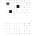
Fig. 9 is that expression is configured to array-like (vertical 6 * horizontal 10) with led chip and the planimetric map of the light source 11 that forms, this figure (a) expression is owing to the individual character difference of each led chip causes the different of the luminous quantity of each led chip and glow color, and the state of evenly not adjusting, the state of the even adjustment of this figure (b) expression having carried out luminous quantity and glow color.
Led chip has photon crystal structure, and the light exit direction is approximately perpendicular to light-emitting area, the directionality height.And, constituting at led chip under the situation of light source 11 by a plurality of photonic crystal type, the interval of led chip is very narrow.
Each led chip is provided with single current supply circuit.Control offers the turn-on time of the current supply of the current value of led chip and time per unit in each current supply circuit.By the Control current value, thereby can control from master (dominant) wavelength of the light of led chip ejaculation.In addition, by the current supply turn-on time of control time per unit, thereby the luminous quantity of led chip is increased and decreased.The even adjustment of the luminous quantity of led chip and glow color as long as adopt visual or sensors such as photographic element, quantizes the luminous quantity of each led chip and glow color to carry out just passable.
Figure 10 is the key diagram of lighting device of the light source 11 of the expression homogenising of having utilized the luminous quantity that carried out in the led chip and glow color.Light source 11 has the area also bigger than display panels 3, and by utilizing lens 23 to converge light beam from light source 11, to meet the size of display panels 3.Through display panels 3 and modulated light is synthesized the image light of other colors by cross-dichroic mirror, and carry out projection.
Figure 11 represent with display panels 3 disposed adjacent in led chip, carried out the light exit side of light source 11 of the homogenising of luminous quantity and glow color.Through display panels 3 and modulated light is synthesized the image light of other colors by cross-dichroic mirror, and carry out projection.
Any structure among Figure 10 and Figure 11 does not possess the light integraph.That is, make in the led chip, carried out the light source 11 of the homogenising of luminous quantity and glow color, thereby can realize not possessing the lamp optical system of light integraph by utilization.In addition, also can make small polarization light conversion device (elementary cell) disposed adjacent constitute led chip or a plurality of led chip of light source 11 in each.Under this situation, also can space (roughly the same with the width of a PBS of elementary cell) be set between the row of the led chip that is configured to array-like and/or between the row.
In the projection display device of above explanation, be not limited to the permeation type liquid crystal display panel, can use the reflective liquid crystal display panel, also can utilize to drive each display panel that becomes the micro-reflector type of pixel and replace these display panels.In addition, though possessed three lighting device 1R, 1G, the 1B of each coloured light of outgoing,, also can constitute with cross-dichroic mirror etc. and carry out beam split or do not carry out beam split and import to the color display panel of veneer as the lighting device of outgoing white light.Under the situation that is made as the lighting device that penetrates white light, each solid-state light emitting element can penetrate white light, also can constitute suitably to arrange the solid-state light emitting element that penetrates ruddiness, blue light, green glow.In addition, solid-state light emitting element is not limited to light emitting diode (LED).
(embodiment 3)
Below, according to Figure 12 and Figure 13 the projection display device of embodiments of the present invention is described.
The projection display device of present embodiment does not possess lighting device, but possesses autoluminescence image display panel 25.Figure 12 is the planimetric map of expression autoluminescence image display panel 25.This autoluminescence image display panel 25 is configured to array-like (being vertical 25 * horizontal 25 among the figure) with led chip and forms.
Led chip has photon crystal structure, and the light exit direction is approximately perpendicular to light-emitting area, and directionality is higher.And, constituting at led chip under the situation of autoluminescence image display panel 25 by a plurality of photonic crystal type, the interval of led chip is very narrow.
Autoluminescence image display panel 25 is connected with not shown driver.The generic drive that this driver can use the autoluminescence image display panel that utilized LED or organic electroluminescent device etc. to use.This driver constitutes has the matrix structure that possesses many signal wires and Duo Gen sweep trace, and possesses signal line drive and scan line driver.Controller in the driver makes scan line driver be selected to the sweep trace of display object, and to each led chip on this sweep trace, uses signal line drive to carry out the current supply control corresponding with received image signal.Current supply control shows in order to carry out gray shade scale, and current value (amplitude) is changed, or the current supply turn-on time of control time per unit (horizontal scan period).
Figure 13 is the figure of optical system of the projection display device of the expression three-plate type that utilizes this autoluminescence image display panel 25.This projection display device possesses three autoluminescence image display panel 25R, 25G, 25B.Autoluminescence image display panel 25R penetrates red image light, and autoluminescence image display panel 25G penetrates green image light, and autoluminescence image display panel 25B penetrates blue image light.The versicolor image light that penetrates from each autoluminescence image display panel 25 is synthesized coloured image light by cross-dichroic mirror 4.This coloured image light is projected lens 5 enlarging projections and is presented on the screen.
Claims (20)
1. a lighting device is characterized in that, comprising:
Possesses the light source that one or more solid-state light emitting elements form;
Make at least one of the photochemical lens of the parallel light that penetrates than the also big optical waveguide of the area of the light entrance face that is arranged in this light source side or described light source from the area of light-emitting face;
First fly lens of the emergent light incident that will penetrate from described optical waveguide or described lens;
Dispose in couples with described first fly lens, light is assembled and be directed to second fly lens on the lighting object.
2. a lighting device is characterized in that, comprising:
Possesses the light source that one or more solid-state light emitting elements form;
With the light exit side disposed adjacent of each solid-state light emitting element, and plural convex lens are distributed to first fly lens of each solid-state light emitting element;
Dispose in couples with described first fly lens, light is assembled and be directed to second fly lens on the lighting object.
3. lighting device according to claim 1 and 2 is characterized in that, at the light exit side of described second fly lens polarized light converting means is set, and it has a plurality of polarised light splitters, to converge direction of polarized light.
4. a lighting device is characterized in that, comprising:
Have a plurality of polarized light beam splitters, to converge the polarized light conversion device of direction of polarized light;
Adjacent one or more solid-state light emitting element that is arranged on the light incident side of described polarized light conversion device;
Will be from the emergent light gathering of polarization light-light conversion device and the optically focused mechanism of guiding lighting object.
5. lighting device according to claim 4 is characterized in that, described optically focused mechanism by first fly lens and with its in pairs second fly lens of configuration form.
6. lighting device according to claim 4 is characterized in that, described optically focused mechanism is the bar type integraph that is tubular or column.
7. lighting device is characterized in that possessing:
The light source of forming by a plurality of solid-state light emitting elements;
Make the luminous quantity and the uniform mechanism of glow color of each solid-state light emitting element.
8. lighting device according to claim 7 is characterized in that, the current value that offers this solid-state light emitting element by control is controlled glow color and luminous quantity.
9. according to claim 7 or 8 described lighting devices, it is characterized in that the current impulse amplitude that offers this solid-state light emitting element by control is controlled luminous quantity.
10. according to each described lighting device in the claim 7~9, it is characterized in that possessing: the light from described light source is not carried out optically focused, but will import the optical system in the lighting object from the light of light source.
11., it is characterized in that, constitute described light source and lighting object disposed adjacent, and will directly import in the lighting object from the light of light source according to each described lighting device in the claim 7~9.
12. according to each described lighting device in the claim 1~11, it is characterized in that, make the asperratio of the asperratio of each solid-state light emitting element and lighting object identical or roughly the same.
13., it is characterized in that solid-state light emitting element is made up of the light emitting diode with photonic crystal according to each described lighting device in the claim 1~12.
14. lighting device according to claim 13 is characterized in that, the light exit direction with light emitting diode of this photonic crystal is approximately perpendicular to light-emitting area.
15. a projection display device, wherein the light that is penetrated from lighting device by display device modulation and carry out projection is characterized in that,
Possess: each described lighting device in the claim 1~14,
And with described display device as lighting object.
16. projection display device according to claim 15 is characterized in that, three described display device are set, to be used for each coloured light; Three institute's lighting devices are set, to be used for each coloured light, will be through carrying out projection after the light compositing of described three display device.
17. a projection display device is characterized in that possessing:
Self-emission display apparatus with a plurality of solid-state light emitting elements that become pixel;
Image light from described self-emission display apparatus is carried out projection lens projecting.
18. projection display device according to claim 17 is characterized in that, three described display device are set, to be used for each coloured light; Three described self-emission display apparatus are set, to be used for each coloured light; Will be through carrying out projection after the light compositing of described three display device.
19., it is characterized in that the solid-state light emitting element in the described display device is made up of the light-emitting diode light with photonic crystal according to claim 17 or 18 described projection display devices.
20. projection display device according to claim 19 is characterized in that, the light exit direction with light emitting diode of described photonic crystal is approximately perpendicular to light-emitting area.
Applications Claiming Priority (2)
| Application Number | Priority Date | Filing Date | Title |
|---|---|---|---|
| JP2004198495 | 2004-07-05 | ||
| JP2004198495A JP2006018196A (en) | 2004-07-05 | 2004-07-05 | Illuminator and projection video display device |
Publications (1)
| Publication Number | Publication Date |
|---|---|
| CN1721978A true CN1721978A (en) | 2006-01-18 |
Family
ID=35513487
Family Applications (1)
| Application Number | Title | Priority Date | Filing Date |
|---|---|---|---|
| CNA2005100824515A Pending CN1721978A (en) | 2004-07-05 | 2005-07-05 | Illuminating device and projection type video display |
Country Status (3)
| Country | Link |
|---|---|
| US (1) | US20060001838A1 (en) |
| JP (1) | JP2006018196A (en) |
| CN (1) | CN1721978A (en) |
Cited By (3)
| Publication number | Priority date | Publication date | Assignee | Title |
|---|---|---|---|---|
| CN101371070B (en) * | 2006-01-19 | 2011-06-08 | 松下电器产业株式会社 | Lighting device and projection display device using same |
| WO2013082794A1 (en) * | 2011-12-09 | 2013-06-13 | 深圳市光峰光电技术有限公司 | Light source and projection system applying same |
| CN103246147A (en) * | 2012-02-13 | 2013-08-14 | 佳能株式会社 | Illumination optical system and image projection apparatus |
Families Citing this family (20)
| Publication number | Priority date | Publication date | Assignee | Title |
|---|---|---|---|---|
| US20070024809A1 (en) * | 2005-07-28 | 2007-02-01 | Victor Company Of Japan, Limited | Polarizing illuminant apparatus and image display apparatus |
| JP5049644B2 (en) | 2006-05-12 | 2012-10-17 | 三洋電機株式会社 | Light source control device and video display device |
| JP5361145B2 (en) * | 2006-06-08 | 2013-12-04 | キヤノン株式会社 | Illumination optical system, image projection optical system, and image projection apparatus |
| KR100797477B1 (en) * | 2006-06-20 | 2008-01-24 | 엘지전자 주식회사 | A display device and illuminating method thereof |
| JP4197527B2 (en) * | 2006-08-18 | 2008-12-17 | 三菱電機株式会社 | Projection display |
| DE102006045440A1 (en) * | 2006-09-26 | 2008-03-27 | Osram Opto Semiconductors Gmbh | Optical projection device comprises light source provided with two light-emitting diode chips, and light source has illumination surface formed by radiation emission surfaces of light-emitting diode chips |
| JP5162901B2 (en) * | 2007-01-05 | 2013-03-13 | 株式会社日立製作所 | Projection display device and optical unit |
| KR100927724B1 (en) | 2008-03-31 | 2009-11-18 | 삼성모바일디스플레이주식회사 | Projection-type display device and driving method thereof |
| US8408721B2 (en) * | 2008-08-14 | 2013-04-02 | 3M Innovative Properties Company | Projection system with imaging light source module |
| JP2010249966A (en) | 2009-04-14 | 2010-11-04 | Hitachi Ltd | Optical engine |
| KR20110002298A (en) * | 2009-07-01 | 2011-01-07 | 삼성전자주식회사 | Illuminating unit and display apparatus having the same |
| JP5504747B2 (en) * | 2009-08-20 | 2014-05-28 | セイコーエプソン株式会社 | projector |
| JP5581629B2 (en) | 2009-08-20 | 2014-09-03 | セイコーエプソン株式会社 | projector |
| JP5436097B2 (en) * | 2009-08-25 | 2014-03-05 | 三菱電機株式会社 | Condensing optical system and projection-type image display device |
| JP5407664B2 (en) * | 2009-08-27 | 2014-02-05 | セイコーエプソン株式会社 | projector |
| JP2012141483A (en) * | 2011-01-05 | 2012-07-26 | Mitsubishi Electric Corp | Design method of led light source device and led light source device |
| TWI484223B (en) * | 2013-01-22 | 2015-05-11 | Machvision Inc | An optical component for multi-angle illumination of line scanning, and a light source system using the same |
| EP3860119A1 (en) | 2013-11-04 | 2021-08-04 | Dolby Laboratories Licensing Corp. | Single modulator projector systems with global dimming |
| JP6911878B2 (en) * | 2019-02-28 | 2021-07-28 | セイコーエプソン株式会社 | Image display device and virtual image display device |
| JP6900961B2 (en) * | 2019-02-28 | 2021-07-14 | セイコーエプソン株式会社 | Image display device and virtual image display device |
Family Cites Families (10)
| Publication number | Priority date | Publication date | Assignee | Title |
|---|---|---|---|---|
| JPH10293545A (en) * | 1997-04-21 | 1998-11-04 | Hitachi Ltd | Projection display device |
| JP4182374B2 (en) * | 1998-10-29 | 2008-11-19 | ソニー株式会社 | Projection display |
| TW380213B (en) * | 1999-01-21 | 2000-01-21 | Ind Tech Res Inst | Illumination apparatus and image projection apparatus includes the same |
| JP2001249400A (en) * | 2000-03-03 | 2001-09-14 | Seiko Epson Corp | Projection-type display apparatus |
| JP2001343706A (en) * | 2000-05-31 | 2001-12-14 | Sony Corp | Video display device |
| US7279718B2 (en) * | 2002-01-28 | 2007-10-09 | Philips Lumileds Lighting Company, Llc | LED including photonic crystal structure |
| JP2003280094A (en) * | 2002-03-22 | 2003-10-02 | Ricoh Co Ltd | Lighting device |
| JP3991764B2 (en) * | 2002-05-10 | 2007-10-17 | セイコーエプソン株式会社 | Illumination device and projection display device |
| JP3989302B2 (en) * | 2002-05-24 | 2007-10-10 | オリンパス株式会社 | Illumination device and projector device |
| US6898358B2 (en) * | 2002-05-31 | 2005-05-24 | Matsushita Electric Industrial Co., Ltd. | Adjustable photonic crystal and method of adjusting the index of refraction of photonic crystals to reversibly tune transmissions within the bandgap |
-
2004
- 2004-07-05 JP JP2004198495A patent/JP2006018196A/en active Pending
-
2005
- 2005-06-30 US US11/169,880 patent/US20060001838A1/en not_active Abandoned
- 2005-07-05 CN CNA2005100824515A patent/CN1721978A/en active Pending
Cited By (5)
| Publication number | Priority date | Publication date | Assignee | Title |
|---|---|---|---|---|
| CN101371070B (en) * | 2006-01-19 | 2011-06-08 | 松下电器产业株式会社 | Lighting device and projection display device using same |
| WO2013082794A1 (en) * | 2011-12-09 | 2013-06-13 | 深圳市光峰光电技术有限公司 | Light source and projection system applying same |
| CN103246147A (en) * | 2012-02-13 | 2013-08-14 | 佳能株式会社 | Illumination optical system and image projection apparatus |
| CN103246147B (en) * | 2012-02-13 | 2015-07-29 | 佳能株式会社 | Illumination optical system is unified image projection device |
| US9223122B2 (en) | 2012-02-13 | 2015-12-29 | Canon Kabushiki Kaisha | Illumination optical system and image projection apparatus |
Also Published As
| Publication number | Publication date |
|---|---|
| US20060001838A1 (en) | 2006-01-05 |
| JP2006018196A (en) | 2006-01-19 |
Similar Documents
| Publication | Publication Date | Title |
|---|---|---|
| CN1721978A (en) | Illuminating device and projection type video display | |
| CN1487356A (en) | Illuminating apparatus and projector display device | |
| CN100350282C (en) | Illuminating system and projector using same | |
| CN1667500A (en) | Illuminating apparatus, image display apparatus, and projector | |
| CN1206567C (en) | Assembly of display device and illumination system | |
| CN1086894C (en) | Light projection method and projection type image display device for realizing said method | |
| CN1782862A (en) | Illuminating device and projection type video display apparatus | |
| CN1782860A (en) | Light source device and image display device | |
| CN101971637B (en) | Projection system based on self emitting display panel | |
| CN1677180A (en) | Semiconductor light-emitting device and video display adopting it | |
| CN1693986A (en) | Image display apparatus | |
| CN1914520A (en) | Light-collecting illumination system | |
| CN1501120A (en) | Projector | |
| US7452736B2 (en) | Surface emitting device, manufacturing method thereof and projection display device using the same | |
| CN1287768A (en) | Light source and display device | |
| CN101542192A (en) | Illumination system and display device | |
| CN1467533A (en) | Image display apparatus having optical scanner | |
| CN1187637C (en) | Optical system of liquid crystal projector | |
| CN1993987A (en) | Time-sequentially pulsed LED light source for image projectors | |
| CN1847954A (en) | Light emitting cluster and direct light emitting type backlight unit having the same and liquid crystal display device having the backlight unit | |
| CN101038372A (en) | Projection type image display apparatus | |
| CN1847974A (en) | Optical member and illuminating device | |
| CN1991499A (en) | Direct light type backlight unit and color filterless liquid crystal display apparatus employing the same | |
| CN1178092C (en) | Lighting optical system and projecting instrument using said optical system | |
| CN1291299A (en) | Illuminator and projection display |
Legal Events
| Date | Code | Title | Description |
|---|---|---|---|
| C06 | Publication | ||
| PB01 | Publication | ||
| C10 | Entry into substantive examination | ||
| SE01 | Entry into force of request for substantive examination | ||
| C02 | Deemed withdrawal of patent application after publication (patent law 2001) | ||
| WD01 | Invention patent application deemed withdrawn after publication |