CN1717624A - Method of forming a rim phase shifting mask and using the rim phase shifting mask to form a semiconductor device - Google Patents
Method of forming a rim phase shifting mask and using the rim phase shifting mask to form a semiconductor device Download PDFInfo
- Publication number
- CN1717624A CN1717624A CNA038189585A CN03818958A CN1717624A CN 1717624 A CN1717624 A CN 1717624A CN A038189585 A CNA038189585 A CN A038189585A CN 03818958 A CN03818958 A CN 03818958A CN 1717624 A CN1717624 A CN 1717624A
- Authority
- CN
- China
- Prior art keywords
- layer
- mask
- opening
- transparency carrier
- opaque
- Prior art date
- Legal status (The legal status is an assumption and is not a legal conclusion. Google has not performed a legal analysis and makes no representation as to the accuracy of the status listed.)
- Pending
Links
Images


Classifications
-
- G—PHYSICS
- G03—PHOTOGRAPHY; CINEMATOGRAPHY; ANALOGOUS TECHNIQUES USING WAVES OTHER THAN OPTICAL WAVES; ELECTROGRAPHY; HOLOGRAPHY
- G03F—PHOTOMECHANICAL PRODUCTION OF TEXTURED OR PATTERNED SURFACES, e.g. FOR PRINTING, FOR PROCESSING OF SEMICONDUCTOR DEVICES; MATERIALS THEREFOR; ORIGINALS THEREFOR; APPARATUS SPECIALLY ADAPTED THEREFOR
- G03F1/00—Originals for photomechanical production of textured or patterned surfaces, e.g., masks, photo-masks, reticles; Mask blanks or pellicles therefor; Containers specially adapted therefor; Preparation thereof
- G03F1/26—Phase shift masks [PSM]; PSM blanks; Preparation thereof
- G03F1/29—Rim PSM or outrigger PSM; Preparation thereof
Landscapes
- Physics & Mathematics (AREA)
- General Physics & Mathematics (AREA)
- Preparing Plates And Mask In Photomechanical Process (AREA)
- Exposure And Positioning Against Photoresist Photosensitive Materials (AREA)
Abstract
A semiconductor device is formed by patterning a resist layer (88) using a rim phase shifting mask (84). A multilayer or single patterning layer to form the different phase-shifting regions (25 or 50 or 26) and opaque regions (64) is used to manufacture the rim phase shifting mask (84). First phase shifting regions are formed by transferring an opening (17) in the multilayer or single patterning layer through an opaque layer (14) and a transparent substrate (12). At least portions of the same multilayer or single patterning layer are used to recess the opaque layer a predetermined distance to form rims (second phase shifting regions) (26). The first phase-shifting regions (25 or 50) phase shift the light traveling through them 180 degrees relative to the light traveling through the rims (26), thereby increasing the contrast of the light traveling through the rim phase shifting mask.
Description
Technical field
The field of the invention relates in general to semiconductor devices, relates more specifically to photoetching technique.
Background technology
For the speed of making great efforts to make more device function be fit to littler zone and increase integrated circuit, dwindled the size of funtion part (feature) (for example, the width of interconnection line) in the integrated circuit.An obstacle that overcomes is: with rational cost, pass graticule (reticle), form the desired pattern with little funtion part in the photoresist layer by illumination radiation (for example, light), promptly be called the reliability of the technology of photoetching technique.Because photoetching technique is subjected to the restriction of diffraction, suppressed to be printed on the funtion part of the minimum in the photoresist layer so pass the scatter phenomenon of (diffraction) of opening time in the graticule by light.If imaging optical system is caught the light less than diffraction, pattern-information is lost and can not constitute little funtion part in the photoresist pattern so.Because imaging optical system contains defectiveness originally, so they can not catch all pattern-informations.Thus, it is desirable diffraction being reduced to minimum.
A kind of method is the optical phase shift photoetching technique, its use has the graticule of the transparent material of patterning, the transparent material of patterning has predetermined thickness, and the light by the transparent material transmission has 180 phase differential of spending with the adjacent area that does not comprise transparent material like this.Resulting interference effect has improved contrast, sharpness and other technological parameter of pattern.
Utilization is for many diverse ways of optical phase shift photoetching technique, with the phase place of the light of other parts skew in the predetermined portions of graticule of relative graticule, reduces diffraction and prints little funtion part making great efforts.One type mask is alternating phase-shift mask (APSM), and it only has 0 degree and 180 degree phase-shifted regions.The major defect of APSM is the boundary between 0 degree and 180 degree phase-shifted regions, and phase conflicts rises, and it may cause unfavorable printed matter, for example is not the line of the part of desired pattern.
Another kind of photoetching method, complementary phase shifting mask (CPSM) by increase by second (non-phase shift) mask with the complementation of first (phase shift) mask, attempts stoping the undesirable phase conflicts effect that produces in APSM.Although solved the phase conflicts problem,, use CPSM to increase cycle, cost and manufacturing complicacy owing to use two masks to form the pattern of expectation.
For overcoming the shortcoming of APSM and CPSM, use flange (rim) phase shifting mask (RPSM).RPSM has the flange that is provided with along the edge in the zone of opaque patternization, and the zone of opaque patternization is generally evanohm and is formed on above the quartz base plate.The region blocks of opaque patternization light, make in photoetching process when using RPSM the photoresist layer on the semiconductor wafer that do not develop in the zone below the zone of opaque patternization.Typically, flange is the groove in the quartz base plate, make the relative quartz base plate of light skew 180 degree,, improved the sharpness and the process tolerant of corresponding function part in the photoresist on the semiconductor wafer thus with the image contrast in the zone of improving opaque patternization.
A kind of method that is used to form RPSM is included in coating photoresist layer on the chromium alloy layer that is deposited on the not composition on the smooth quartz base plate.The first photoresist layer patterned and as mask with etching chromium alloy at first, and enter quartzy with after etching to form flange.Because flange extremely little (the approximately size of the evanohm of the adjacent patternsization of 10-20%) is so the quartzy etching of control is very important well.After forming flange, remove the first photoresist layer and coating and the composition second photoresist layer on chromium alloy layer.Use the second photoresist pattern as the mask etching chromium alloy layer.Retreat the etching evanohm from quartzy flange after, the second photoresist layer makes the remainder of chromium alloy layer between flange to the aligning of quartz base plate flange.Because carried out two photoetching processes (that is, the photoresist pattern step), so said method still is problematic, it has increased manufacturing time and cost.Therefore, have the needs for the controllable method that forms RPSM, wherein RPSM makes flange aim at the evanohm of composition voluntarily and manufacturing time and cost is reduced to minimum.
Description of drawings
The present invention illustrates by means of example but is not limited to accompanying drawing, and wherein identical mark is represented similar element, and wherein:
Fig. 1 to 7 example according to the sectional view of the formed flange phase shifting mask of first embodiment of the invention;
Fig. 8 to 13 example according to the sectional view of the formed flange phase shifting mask of second embodiment of the invention;
Figure 14 to 19 example according to the sectional view of the formed flange phase shifting mask of further embodiment of this invention;
Figure 20 example use the arbitrary flange phase shifting mask that in the various embodiment of example shown in Fig. 1 to 19, forms to be formed on the method for the photoresist layer on the semiconductor wafer with composition.
It will be understood by those skilled in the art that for simple and understand and example the element among the figure, but needn't draw by specification.For example, some size of component among the figure is other possible being exaggerated of element relatively, to help to improve the understanding of embodiments of the invention.
Embodiment
When forming semiconductor devices, light passes graticule with the resist on the composition semiconductor wafer (photoresist) layer.For improving the pattern on the resist layer, on resist, during incident light, can increase the contrast of light by using flange phase shift graticule or mask (RPSM).Can utilize multilayer or single layer mask film to form RPSM and come composition opaque layer and transparency carrier, to form first phase-shifted region and flange.According to embodiments of the invention, flange does not carry out phase deviation and the not etched quartz base plate that enters to light.But first phase-shifted region makes light opposing flanges phase deviation 180 degree that passes it, and enters transparency carrier by etched recesses or groove and form.By being caved in, opaque layer forms flange.First phase-shifted region and flange all are to utilize the part of multilayer or single layer mask film to form.
The first embodiment of the present invention is a kind of method of using bilayer mask film to form phase shifting mask.The top layer composition transparency carrier of bilayer mask film, and make the bottom depression form flange with etching (following) opaque layer.In a second embodiment, use the tri-layer mask film to form RPSM.The top layer of mask film is used for the middle layer of patterned mask film, and it is used for the bottom and the opaque layer of patterned mask film again.Bottom is the mask that is used for the composition transparency carrier.In the 3rd embodiment, use same photoresist individual layer etching transparency carrier and on the opaque layer covered.Understand each embodiment better by means of accompanying drawing.
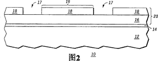
Among Fig. 1 to 7 example utilize first embodiment to be used to form the method for RPSM.The part of first graticule or RPSM10 has been shown among Fig. 1, first graticule or RPSM10 (for example are included in opaque layer 14, evanohm or chromium) and the bilayer mask film 20 (for example, double-deck photoresist) that forms above of transparency carrier 12 (for example, quartz).In one embodiment, the opaque layer 14 that is formed by physical vapor deposition (PVD) is approximately the evanohm of 100 nanometers (on thickness).Bilayer mask film 20 comprises the end (following or pattern) layer 16 and top (image) layer 18.In one embodiment, bottom 16 is different resist layers with top layer 18.As below becoming apparent, in the embodiment shown in Fig. 1 to 7, when composition or imageization top layer 18, the composition bottom 16.A kind of method that obtains such effect is, when double-deck mask 20 was exposed to the light that is used for composition or electron source, top layer 18 had the exposure light sensitivity higher than bottom 16.In a preferred embodiment, if top layer is siliceous resist layer, for example silane or silicon silsequioxane (silsequioxane), and bottom 16 is alkyd resin based (novolak-based) materials, this situation will occur so.Yet, when composition can be for the top layer 18 of any polymkeric substance, organic material and so on, bottom 16 can or be incited somebody to action not patterned any other material for any polymeric material (for example, resist), organic material (for example, polyimide or indefinite form carbon).
As shown in Figure 2, use known photoetching process, for example electron beam direct writes photoetching (EBL), electron beam projection lithography (EPL) or any other optical lithography pattern generating technology, and composition top layer 18 is to expose bottom 16 in first opening 17.Although among the embodiment in the accompanying drawings, first opening 17 appears as two different openings in cross sectional view, but from top view, first opening 17 is the rectangles around all sidewalls of the part of composition 19 of top layer 18, and therefore will be called single opening.Yet, those skilled in the art will appreciate that first opening 17 needn't form rectangle from top view, but can use any other shape or the design that is used for composition top layer 18.The pattern that is used for the top layer 18 and first opening 17 will depend on the pattern that the photoresist layer is expected, it is patterned as the part of the technology that forms semiconductor devices subsequently, is described in more detail as following.
As shown in Figure 3, after forming first opening 17, etching bottom 16 and opaque layer 14 are to form bottom 16 and the opaque layer 14 that second opening, 22, the second openings 22 extend into first opening 17.In other words, the design transfer of top layer 18 is on bottom 16 and opaque layer 14.In one embodiment, particularly,, use so to contain the part that the oxygen chemical agent is removed bottom 16 if bottom 16 is polymeric material, for example resist; If opaque layer is material, for example evanohm that contains chromium, use chloride and chemical agent oxygen to remove part opaque layer 14 so.Arrive bottom 16 with the formation opening owing to use different chemical agents to come etching bottom 16 and opaque layer 14, the first openings 17 will at first shift (transfer), and subsequently etching opaque layer 14 is finished second opening 22.For the sake of simplicity, etching bottom 16 and opaque layer 14 resulting structure afterwards has been shown among Fig. 3.
In case in top layer 18, bottom 16 and opaque layer 14, form second opening 22, just remove the partially transparent substrate 12 that exposes by second opening 22 to form the 3rd opening 24.Usually, because top layer 18 and transparency carrier 12 can be by same chemical agent etchings, so in etching transparency carrier 12, will remove the remainder of top layer 18.For example, if transparency carrier 12 is quartzy, top layer 18 is a silicon nitride, can use fluorine-containing chemical agent to come composition transparency carrier 12 so and removes top layer 18.Thereby bottom 16 usefulness act on the mask of etching transparency carrier 12.Since use top layer 18 as the mask composition bottom 16, so in this stage of technology, bottom 16 will have the pattern substantially the same with top layer 18 when exposing at first.(for example, because the manufacturing and the technique change that occur during the photic resist layer 16 in etching bottom may make pattern slightly different.) formation of the 3rd opening 24 is created in first phase-shifted region 25 below the 3rd opening 24, as shown in Figure 4.
First phase-shifted region 25 is the zones that make the phase deviation of the radiation (for example, light) of passing them during photoetching process.In a preferred embodiment, first phase-shifted region 25 is 180 degree phase-shifted regions, and this is because they are thinner than other zone of transparency carrier 12.Determine the thickness of first phase-shifted region 25 by following formula:
d=λ/[2(n-1)]
Wherein d is the thickness of first phase-shifted region 25, and λ is the wavelength that RPSM10 goes up the radiation of incident, and n is the refractive index of transparency carrier 12.First phase-shifted region 25 makes the not layout area of exposing skew 180 degree of the relative RPSM of phase place that passes these regional radiation, and the not layout area of exposing of RPSM did not also form in this stage of technology.In other words, also do not form flange (second phase-shifted region).
Be to form flange, by in photoetching process, making bottom 16 exposures or with containing oxygen chemical agent isotropic etching bottom 16, lateral recesses bottom 16 forms the 4th opening 27 with the top section of expanding the 3rd opening 24.(in addition, during lateral recesses technology, the thickness of bottom 16 can reduce the amount of the lateral recesses amount that equals bottom 16.Therefore, the thickness of bottom 16 will be thicker than the desired amount of wanting lateral recesses before lateral recesses, so that do not remove whole bottoms 16 during this composition technology.Thereby), the border of the 4th opening 27 (external margin) extends to beyond the border of the 3rd opening 24.In other words, the width of the 4th opening 27 is bigger than the width of the 3rd opening 24.In addition, the 4th opening 27 is coaxial with the 3rd opening 24.By lateral recesses bottom 16, expose the part of opaque layer 14.As shown in Figure 5, because before depression bottom 16, the basic coplane in edge of bottom 16 and opaque layer 14 is so the amount of recess of bottom 16 equals the amount of the opaque layer 14 exposed.
As shown in Figure 6, after forming opening 27, remove the exposed portions serve of (depression) opaque layer 14.If opaque layer 14 can be used chloride and chemical agent oxygen for containing the material of chromium so.Depression opaque layer 14, the basic once more coplane of opaque layer 14 and bottom 16 after making.Because the partially transparent substrate that the result exposed 12 of depression opaque layer 14 is flange 26 (second phase-shifted region or table section), the flange 26 basic non-migrations phase place of passing its light in a preferred embodiment.Because the thickness of second phase-shifted region 26 approximates K greatly and multiply by light wavelength divided by refractive index, wherein K is an integer, so phase deviation does not take place light.From the phase differential between the light of first phase-shifted region 25 and flange 26 is 180 degree.Thereby in alternative embodiment, flange 26 is second phase-shifted region, and makes light phase skew 270 degree, and first phase-shifted region 25 makes light phase skew 90 degree.As shown in Figure 6, flange 26 be adjacency and the edge on the either side of first phase-shifted region 25.The zone that is covered by the opaque layer 14 of adjacent flanges 26 is place 28.
After forming flange 26, in an embodiment who uses cineration technics, remove bottom 16, cineration technics is to use the etch process of oxygen plasma.After removing bottom 16, finish and example goes out in Fig. 7 first graticule 10 or more specifically be first phase shifting mask.As below becoming apparent, the opaque layer 14 that is formed on above the place 28 has stopped the radiation that is incident on first graticule 10 basically, and first phase-shifted region 25 makes phase place opposing flanges 26 skews 180 degree of light, and flange 26 is under the situation that does not make the light phase shift, transmit radiation by transparency carrier 12, with the little funtion part of composition in the resist layer that on Semiconductor substrate, forms.
Fig. 8 to 13 example be used to form second embodiment of phase shifting mask according to the present invention.Second graticule 30 comprises similar transparency carrier 32 and the opaque layer 34 of equivalent layer (for example, transparency carrier 12 and opaque layer 14) with first graticule 10.Three layer laminate 36 that comprise the end (mask) layer 38, middle (hard mask) layer 40 and top (mask) layers 42 be formed on opaque layer 34 above, as shown in Figure 8.Bottom 38 and top layer 42 can be identical materials, for example resist (for example, novolak-based material).Yet in one embodiment, bottom 38 is different materials (for example, bottom 38 is a novolak-based material, and top layer 42 is siliceous resist layers) with top layer 42.Middle layer 40 can be resist layer or oxide skin(coating), for example HSQ (hydrogen silicon silsequioxane) or monox (SiO
2).Selection is used for material top layer 42 and all optionally exposure or etchings of bottom 38 relatively in middle layer 40.In one embodiment, be used for thickness from 50 to the 300 nanometers variation of these layers.More specifically, the thickness of top layer 42 approximates 50 nanometers greatly, and the thickness of bottom 38 is approximately 300 nanometers, and the thickness in middle layer 40 is between about 50 to 300 nanometers.
As shown in Figure 9, use known photoetching process composition top layer 42 to form first opening 44 in exposed portions serve middle layer 40.Although first opening 44 is shown as two openings in cross sectional view, identical with first opening 17 of first embodiment, first opening 44 is actually an opening.
As shown in Figure 10, after forming first opening 44, etching middle layer 40 extends into second opening 46 in the middle layer 40 of first opening 44 with formation.For monox bottom 38 is among the embodiment of resist, can use the chemical agent that contains fluorocarbon to come in middle layer 40 to bottom 38 selective etch middle layers 40.
After forming second opening 46, etching bottom 38 extends into the 3rd opening 48 in the bottom 38 of second opening 46 with formation, as shown in Figure 11 example.If top layer 42 is and bottom 38 identical materials, at least a portion that in composition bottom 38, will remove top layer 42 so, this is because when etching bottom 38, top layer 42 is exposed in itself the chemical agent of etching.For the whole top layers 42 that will remove when the composition bottom 38, top layer 42 will be less than or equal to the thickness of bottom 38.In a preferred embodiment, top layer 42 is obviously thin than bottom 38, to guarantee removing all top layers 42 when the composition bottom 38.Thereby, the additional technical steps that does not need to remove top layer 42.If during composition top layer 38, removed top layer 42, will not remove middle layer 40 (that is, based etch chemistry is optionally for middle layer 40) so, so that middle layer 40 can be with the mask that acts on composition bottom 38.
In another embodiment, if top layer 42 is not then removed together with the mask that acts on composition bottom 38 in top layer 42 and middle layer 40 when composition bottom 38.Yet if top layer 42 can be with the mask that acts on composition bottom 38, middle layer 40 just not necessarily so, and replace three layer laminate 36, should use the double-deck lamination of example shown in first method to reduce technology (for example, the deposit in middle layer 40), and reduce manufacturing cycle time thus.
As shown in Figure 12, behind composition bottom 38, it is the extensions that enter the last opening of opaque layer 34 and transparency carrier 32 that etching opaque layer 34 and transparency carrier 32 form the 4th opening 52, the four openings 52.Because material can be identical, so can use the above-mentioned chemical agent that is used for etching opaque layer 14 and transparency carrier 12 in first embodiment, comes etching transparency carrier 32 and opaque layer 34.Usually, will remove middle layer 40 in etching transparency carrier 32, bottom 38 usefulness act on the mask of etching transparency carrier 32 like this.Be that first phase-shifted region, 50, the first phase-shifted regions 50 are similar to first phase-shifted region 25 of first graticule 10 below the 4th opening 52.
Be used to finish the technology of manufacturing second graticule 30 with identical at the described technology of Fig. 5 to 7 of first embodiment.After forming first phase-shifted region 50, depression bottom 38 to be to expand the top section of the 4th opening 52, and top section (the 5th opening, not shown) has the border that extends in the 4th opening and the part border in addition of opaque layer 34 like this.The exposed portions serve of removing opaque layer 34 subsequently is to form flange (second phase-shifted region) 54, as shown in Figure 13.Then, remove bottom 38, wherein carry out with cineration technics in one embodiment.Resulting second graticule (second phase shifting mask) 30 has place 53, first phase-shifted region 50 and the flange 54 that is positioned at below the opaque layer 34, they are similar and all be used for layer on the composition semiconductor wafer with the equivalence zone of first graticule, describe in detail as following.
Figure 14 to 19 example be used to form the third method of phase shifting mask according to the present invention.The 3rd graticule 60 among Figure 14 comprises the resist layer 66 that overlays on above the opaque layer 64, and opaque layer 64 is formed on the transparency carrier 62.In one embodiment, opaque layer 64 is evanohm of 100 nanometers (on thickness) that form with PVD, and resist layer is about at least 500 nanometers of forming with spin coating technique, more specifically is approximately the resist of 500 to 700 nanometers.Equivalent layer among the embodiment of transparency carrier 62 and opaque layer 64 and front is similar.
As shown in Figure 15, composition resist layer 66 extends through resist layer 66 and exposes opaque layer 64 to form first opening, 68, the first openings 68.Can use the photoetching process of any routine to form first opening 68.Although when first opening 68 similar to first opening in the previous embodiment observed, be shown as two openings on the cross section, it is an opening., on transparency carrier 62, do not form extra resist layer and be used for follow-up composition with after forming first opening 68 at the composition resist layer.
After forming first opening 68, the opaque layer 64 of removing in first opening 68 extends through resist layer 66 and opaque layer 64 to form second opening, 70, the second openings 70, as shown in Figure 16.If opaque layer 64 is an evanohm, can use chloride and oxygen containing chemical agent to come etching opaque layer 64.
As shown in Figure 17, in one embodiment, enter transparency carrier 62, make second opening 70 extend into transparency carrier 62, to form the 3rd opening 72 by utilizing fluorine-containing chemical agent etched recesses (groove).By making a part of attenuation of transparency carrier 62, it is similar to form first phase-shifted region that forms in first phase-shifted region, 71, the first phase-shifted regions 71 and the previous embodiment.In other words, first phase-shifted region 71 is 180 degree phase-shifted regions.
After forming first phase-shifted region 71, resist layer 66 and the opaque layer 64 of caving in simultaneously is coaxial and have a border in addition, border that extends in the 3rd opening 72 with the 3rd opening 72 to form the 4th opening 73, the four openings 73 together.The exposed portions serve of the transparency carrier 72 in groove is not flanges 74, and flange 74 is zero degree phase-shifted regions of the 3rd mask 60.Flange 74 is in abutting connection with opaque layer 64, and opaque layer 64 covers place 76.
In the 3rd embodiment, use single resist layer 66 (that is not being multilayer laminated) to form first phase-shifted region 71 and flange 74.Owing in whole composition technology, will keep quite a few of resist layer, need suitable resist layer.Preferably, resist layer is approximately greater than 500 nanometers, or more preferably between about 500 and 700 nanometers.Thereby, in one embodiment, can use the thick resist layer.In the method for prior art, do not use the thick resist layer to come the little size of composition, flange for example, this is because controlled composition resist forms the restriction of the technology of little funtion part.But the applicant has overcome this problem by determining chemical agent and other etching parameter, makes it possible to utilize the individual layer resist layer controllably to form flange.
In one embodiment, if opaque layer 64 is evanohm, can utilize 7: 1 to 1: 1 so, be approximately 7: 1 more specifically or the chlorine of about 5: 1 ratios than the etch process of the oxygen evanohm that caves in.This chemical agent single monolayer thick resist layer 66 that also caves in.The degree of depression single monolayer thick resist layer 66 depends on the selectivity of single monolayer thick resist layer 66 of the chemical agent of the evanohm that is used to cave in.In a preferred embodiment, the amount of recess of evanohm and resist about equally.In the present embodiment, use the oxygen of 1 to 200sccm chlorine and 1 to 200sccm as based etch chemistry.Can add extra gas, for example argon to chlorine and oxygen.In one embodiment, power can be about at least 200 watts, and RF (radio frequency) bias power that imposes on reaction chamber can be less than or equal to about 300 watts.Used in one embodiment pressure is between 1 to 300 millitorr (mT), more specifically between 1 to 100mT.In a preferred embodiment, the air-flow of the chlorine of 35sccm (standard cubic centimeter) and the oxygen of 9sccm is as based etch chemistry, and this based etch chemistry has following parameters for reactive ion etching (RIE) instrument: the RF power of the pressure of 10mT, 15W and the power of 500W.Those skilled in the art will appreciate that for different instruments and can change used condition, particularly power and pressure.After forming flange 74, remove thick individual layer resist layer 66, produce the 3rd graticule (phase shifting mask) 60, the three graticules 60 and the final phase shifting mask that forms with previous embodiment in the operating aspect equivalence.
In all embodiment, use identical resist layer (multilayer or individual layer) to form first phase-shifted region and flange.By utilizing identical resist layer, eliminated repeatedly consuming and expensive photoetching process, reduced cycle and manufacturing cost thus.Use another advantage of above-mentioned any embodiment to be, use voluntarily that Alignment Process makes flange aim at first phase-shifted region and place, therefore eliminated out-of-alignment possibility.By reducing out-of-alignment possibility, obtained to increase the more durable technology of output.Equally,, can carry out all being etched with at same system and reduce operation, reduce cost and defective thus and produced according to the foregoing description.Above-mentioned certain methods also makes it possible to make the variable-sized flange with excellent homogeneity.In other words, all flanges do not need to be identical size.For example, in order to form the flange of different size, suitably composition multilayer or single layer mask.In other words, the pattern of the flange in multilayer or single layer mask will be of different sizes.
Although not shown, when the layer below the etching, can on thickness, reduce any layer (for example, resist layer) that exposes.For example, in the 3rd embodiment, when etching transparency carrier 62, can on thickness, reduce resist layer 66, to form first phase-shifted region 71 among Figure 17.In one embodiment, resist thickness can reduce about 5-10% of original thickness.
Can carry out above-mentioned those technologies extra technology in addition.For example, in any resist layer (multilayer or individual layer), form after above-mentioned any opening, can use oxygen plasma to eliminate residue technology, to improve opening and to remove any resist residue that from resist layer composition technology, produces.
In addition, may damage opaque layer when forming flange when composition.For avoiding this damage, with before forming flange, can utilize backside exposure to come composition resist layer (multilayer or individual layer) in the depression opaque layer.This most probable uses in conjunction with the 3rd embodiment.
In above-mentioned instructions, the present invention has been described with reference to specific embodiment.Yet those of ordinary skill in the art should understand below not breaking away from the claim and can be used as various modifications and variations under the situation of illustrated scope of the present invention.Therefore, it is illustrative and not restrictive that instructions and accompanying drawing should be regarded as, and all such modifications and variations are included in the scope of the present invention.
The method of having introduced income, other advantage and having dealt with problems at specific embodiment above.But, can make any income, advantage or method appearance or become significant more income, advantage, the method for dealing with problems and any parts not answer inference is key, necessary or main feature or parts any or that all authority requires.As used herein, term " comprises (comprise) ", " constituting (comprising) " or its any other variation want to cover the inclusion of not getting rid of, make to comprise that technology, method, article or the equipment of row parts not only comprise those parts, but also can comprise technology that clearly do not list or this, method, article or the intrinsic miscellaneous part of equipment.
Claims (10)
1. method that forms the flange phase shifting mask comprises:
Transparency carrier is provided;
Form the opaque layer (14 or 34) that covers described transparency carrier (12 or 32);
Form first mask layer (16 or 38) that covers described opaque layer;
Form second mask layer (18 or 42) that covers first mask layer (17 or 46);
Described second mask layer of composition is to limit first opening;
Shift first opening (17,22 and 24 or 46,48 and 52) and pass described second mask layer and opaque layer and enter transparency carrier, with first phase-shifted region (25 or 50) that exposes described transparency carrier;
Cave in first mask layer (16 among Fig. 5 or 38) to form second opening (24 among Fig. 5), and the external margin of described second opening extends to beyond the external margin of described first opening;
Remove the part that in second opening, covers the opaque layer of described transparency carrier, with the ledge zone (26) that exposes described transparency carrier; And
Remove described first and second mask layers to form described flange phase shifting mask.
2. according to the process of claim 1 wherein, described first mask layer comprises novolak-based material.
3. according to the process of claim 1 wherein, described first phase-shifted region (25 or 50) makes light pass radiation phase deviation 180 degree of ledge zone (26) relatively.
4. according to the process of claim 1 wherein, described second opening is coaxial with described first opening.
5. according to the method for claim 1, further comprise:
Form the 3rd mask layer (40) that covers first mask layer (38), wherein second mask layer (42) covers described the 3rd mask layer.
6. according to the method for claim 5, wherein, described formation first opening comprises:
Shift first opening (7,22 and 24 or 46,48 and 52) and pass the 3rd mask layer (40),
Utilize the 3rd mask layer (40) to form to pass first opening of first mask layer (38) and opaque layer (34), and
Remove the 3rd mask layer (40).
7. according to the method for claim 6, wherein, each all comprises anticorrosive additive material for first mask layer (16 or 38) and second mask layer (18 or 42), and the 3rd mask layer (40) comprises hard mask.
8. method that forms the flange phase shifting mask comprises:
Transparency carrier (12,32 or 62) is provided;
Form the opaque layer (14,34 or 64) that covers described transparency carrier;
Form the resist layer (16,38 or 66) that covers described opaque layer;
The described resist layer of composition is to limit first opening (22,48 or 68);
Shift described first opening and pass described opaque layer and enter described transparency carrier, with first phase-shifted region (25,50 or 71) that exposes transparency carrier;
Depression covers above the described transparency carrier and the part of the opaque layer below described resist layer (14,34 or 64);
When the part of the described opaque layer of depression, the part of depression resist layer (16,38 or 66); And
After the part of the described opaque layer of depression, remove resist layer (16,38 or 66) to form described flange phase shifting mask.
9. method according to Claim 8 wherein, is opened (22,48 or 68) afterwards and before removing described resist layer at composition resist layer (16,38 or 66) to limit first, does not form extra resist layer.
10. method that is used to form semiconductor devices:
Semiconductor substrate (89) is provided;
On Semiconductor substrate (89), form resist layer (88);
Flange phase shifting mask (84) is provided, and described flange phase shifting mask (84) is formed by following method, comprising:
Transparency carrier (12 or 32) is provided;
Form the opaque layer (14 or 34) that covers described transparency carrier;
Form first mask layer (16 or 38) that covers described opaque layer;
Form second mask layer (18 or 42) that covers described first mask layer;
Described second mask layer of composition is to limit first opening (17 or 46);
Shift first opening (17,22 and 24 or 46,48 and 52) and pass described second mask layer and opaque layer, and enter described transparency carrier, with first phase-shifted region (25 or 50) that exposes described transparency carrier;
Cave in first mask layer (16 among Fig. 5 or 38) to form second opening (24 among Fig. 5), and the external margin of described second opening extends to beyond the external margin of described first opening;
Remove the part that in described second opening, covers the opaque layer of described transparency carrier, with the ledge zone (26) of exposing described transparency carrier;
Remove described first and second mask layers to form described flange phase shifting mask; And
Radiation source (81) is provided, makes it by flange phase shifting mask (84) to semiconductor substrate (89), to go up the pattern that forms exposure at resist layer (88).
Applications Claiming Priority (2)
| Application Number | Priority Date | Filing Date | Title |
|---|---|---|---|
| US10/213,344 | 2002-08-06 | ||
| US10/213,344 US6797440B2 (en) | 2002-08-06 | 2002-08-06 | Method of forming a rim phase shifting mask and using the rim phase shifting mask to form a semiconductor device |
Publications (1)
| Publication Number | Publication Date |
|---|---|
| CN1717624A true CN1717624A (en) | 2006-01-04 |
Family
ID=31494444
Family Applications (1)
| Application Number | Title | Priority Date | Filing Date |
|---|---|---|---|
| CNA038189585A Pending CN1717624A (en) | 2002-08-06 | 2003-05-15 | Method of forming a rim phase shifting mask and using the rim phase shifting mask to form a semiconductor device |
Country Status (7)
| Country | Link |
|---|---|
| US (1) | US6797440B2 (en) |
| EP (1) | EP1529246A1 (en) |
| JP (1) | JP2005534978A (en) |
| CN (1) | CN1717624A (en) |
| AU (1) | AU2003232155A1 (en) |
| TW (1) | TWI228207B (en) |
| WO (1) | WO2004013694A1 (en) |
Cited By (3)
| Publication number | Priority date | Publication date | Assignee | Title |
|---|---|---|---|---|
| CN102279517A (en) * | 2010-06-14 | 2011-12-14 | 清华大学 | Nano-imprinting method |
| CN107424954A (en) * | 2016-05-23 | 2017-12-01 | 台湾积体电路制造股份有限公司 | The manufacture method of semiconductor structure |
| CN107427964A (en) * | 2015-03-17 | 2017-12-01 | Ap系统股份有限公司 | Device using laser patterning manufacture shadow mask and the method using laser patterning manufacture shadow mask |
Families Citing this family (11)
| Publication number | Priority date | Publication date | Assignee | Title |
|---|---|---|---|---|
| US6913868B2 (en) * | 2003-01-21 | 2005-07-05 | Applied Materials, Inc. | Conductive bi-layer e-beam resist with amorphous carbon |
| KR100571411B1 (en) * | 2003-12-27 | 2006-04-14 | 동부아남반도체 주식회사 | Mask of semiconductor device and pattern formation method thereof |
| KR100652388B1 (en) * | 2004-11-30 | 2006-12-01 | 삼성전자주식회사 | Focus monitoring mask having multi-phase phase shifter and method for fabricating the same |
| US20070012335A1 (en) * | 2005-07-18 | 2007-01-18 | Chang Hsiao C | Photomask cleaning using vacuum ultraviolet (VUV) light cleaning |
| US7381618B2 (en) * | 2006-10-03 | 2008-06-03 | Power Integrations, Inc. | Gate etch process for a high-voltage FET |
| US20080146001A1 (en) * | 2006-12-15 | 2008-06-19 | Texas Instruments Inc. | Pre-STI nitride descum step for increased margin against STI seam voids |
| JP2009025553A (en) * | 2007-07-19 | 2009-02-05 | Canon Inc | Phase shift mask |
| KR100950481B1 (en) | 2008-06-26 | 2010-03-31 | 주식회사 하이닉스반도체 | Method for fabricating hole-type pattern using photomask |
| US20120098124A1 (en) * | 2010-10-21 | 2012-04-26 | Taiwan Semiconductor Manufacturing Company, Ltd. | Semiconductor device having under-bump metallization (ubm) structure and method of forming the same |
| JP2012099178A (en) * | 2010-11-02 | 2012-05-24 | Hoya Corp | Imprint mold for bit-patterned medium manufacturing, and manufacturing method thereof |
| US11131919B2 (en) * | 2018-06-22 | 2021-09-28 | International Business Machines Corporation | Extreme ultraviolet (EUV) mask stack processing |
Family Cites Families (14)
| Publication number | Priority date | Publication date | Assignee | Title |
|---|---|---|---|---|
| US6007324A (en) | 1977-10-23 | 1999-12-28 | Taiwan Semiconductor Manufacturing Company, Ltd. | Double layer method for fabricating a rim type attenuating phase shifting mask |
| US5126006A (en) | 1990-10-30 | 1992-06-30 | International Business Machines Corp. | Plural level chip masking |
| EP0567419A2 (en) | 1992-04-23 | 1993-10-27 | International Business Machines Corporation | A shifter-based rim phase shifting structure and process to fabricate the same |
| US5302477A (en) | 1992-08-21 | 1994-04-12 | Intel Corporation | Inverted phase-shifted reticle |
| US5403682A (en) | 1992-10-30 | 1995-04-04 | International Business Machines Corporation | Alternating rim phase-shifting mask |
| JP2500050B2 (en) | 1992-11-13 | 1996-05-29 | インターナショナル・ビジネス・マシーンズ・コーポレイション | Method for forming rim type phase shift mask |
| US5495959A (en) | 1994-05-11 | 1996-03-05 | Micron Technology, Inc. | Method of making substractive rim phase shifting masks |
| US6224724B1 (en) | 1995-02-23 | 2001-05-01 | Tokyo Electron Limited | Physical vapor processing of a surface with non-uniformity compensation |
| US5536606A (en) | 1995-05-30 | 1996-07-16 | Micron Technology, Inc. | Method for making self-aligned rim phase shifting masks for sub-micron lithography |
| US5955222A (en) * | 1996-12-03 | 1999-09-21 | International Business Machines Corporation | Method of making a rim-type phase-shift mask and mask manufactured thereby |
| TW352421B (en) * | 1998-04-27 | 1999-02-11 | United Microelectronics Corp | Method and process of phase shifting mask |
| KR100295049B1 (en) * | 1998-07-23 | 2001-11-30 | 윤종용 | Method for manufacturing phase shift masks |
| US6582856B1 (en) * | 2000-02-28 | 2003-06-24 | Chartered Semiconductor Manufacturing Ltd. | Simplified method of fabricating a rim phase shift mask |
| US6387787B1 (en) | 2001-03-02 | 2002-05-14 | Motorola, Inc. | Lithographic template and method of formation and use |
-
2002
- 2002-08-06 US US10/213,344 patent/US6797440B2/en not_active Expired - Lifetime
-
2003
- 2003-05-15 AU AU2003232155A patent/AU2003232155A1/en not_active Abandoned
- 2003-05-15 JP JP2004525977A patent/JP2005534978A/en active Pending
- 2003-05-15 WO PCT/US2003/015590 patent/WO2004013694A1/en active Application Filing
- 2003-05-15 EP EP03766809A patent/EP1529246A1/en not_active Withdrawn
- 2003-05-15 CN CNA038189585A patent/CN1717624A/en active Pending
- 2003-06-03 TW TW092115104A patent/TWI228207B/en not_active IP Right Cessation
Cited By (4)
| Publication number | Priority date | Publication date | Assignee | Title |
|---|---|---|---|---|
| CN102279517A (en) * | 2010-06-14 | 2011-12-14 | 清华大学 | Nano-imprinting method |
| CN107427964A (en) * | 2015-03-17 | 2017-12-01 | Ap系统股份有限公司 | Device using laser patterning manufacture shadow mask and the method using laser patterning manufacture shadow mask |
| CN107427964B (en) * | 2015-03-17 | 2019-06-25 | Ap系统股份有限公司 | Device using laser patterning manufacture shadow mask and the method using laser patterning manufacture shadow mask |
| CN107424954A (en) * | 2016-05-23 | 2017-12-01 | 台湾积体电路制造股份有限公司 | The manufacture method of semiconductor structure |
Also Published As
| Publication number | Publication date |
|---|---|
| TW200405134A (en) | 2004-04-01 |
| WO2004013694A1 (en) | 2004-02-12 |
| US20040029021A1 (en) | 2004-02-12 |
| US6797440B2 (en) | 2004-09-28 |
| EP1529246A1 (en) | 2005-05-11 |
| TWI228207B (en) | 2005-02-21 |
| AU2003232155A1 (en) | 2004-02-23 |
| JP2005534978A (en) | 2005-11-17 |
Similar Documents
| Publication | Publication Date | Title |
|---|---|---|
| JP4686006B2 (en) | Halftone phase shift photomask, blank for halftone phase shift photomask, and method for manufacturing halftone phase shift photomask | |
| JP6601245B2 (en) | Photomask blank, photomask manufacturing method, and mask pattern forming method | |
| TWI479257B (en) | Photomask blank, photomask and its manufacturing method | |
| CN1717624A (en) | Method of forming a rim phase shifting mask and using the rim phase shifting mask to form a semiconductor device | |
| US7846617B2 (en) | Pattern forming method and phase shift mask manufacturing method | |
| JPH0798493A (en) | Phase shift mask and its production | |
| US5888678A (en) | Mask and simplified method of forming a mask integrating attenuating phase shifting mask patterns and binary mask patterns on the same mask substrate | |
| US6333213B2 (en) | Method of forming photomask and method of manufacturing semiconductor device | |
| US7846619B2 (en) | Hybrid photomask and method of fabricating the same | |
| US20050202323A1 (en) | Phase shift mask and method of manufacturing phase shift mask | |
| JPH06308713A (en) | Phase shift photomask and blank for phase shift photomask | |
| JP2002164282A (en) | Method of forming pattern using two alternating phase inversion mask | |
| US20090053620A1 (en) | Blank Mask and Method for Fabricating Photomask Using the Same | |
| US7033947B2 (en) | Dual trench alternating phase shift mask fabrication | |
| TW202248744A (en) | Phase-shifting mask and the manufacturing method thereof | |
| US7824824B2 (en) | Composite phase shifting lithography mask including etch stop layer | |
| JP2002268201A (en) | Method for producing phase shift photomask and blank for the same | |
| JPH08297357A (en) | Production of edge enhancement type phase shift mask | |
| TWI652543B (en) | Method for manufacturing the photomask | |
| JP2002244270A (en) | Manufacturing method for phase shift mask and phase shift mask | |
| JPH07281414A (en) | Phase shift mask blank and phase shift mask as well as its production | |
| TW202217439A (en) | Manufacturing method of photomask and photomask blank | |
| JPH0588353A (en) | Production of exposing mask | |
| JPH07306522A (en) | Phase shift photomask | |
| JPH05241320A (en) | Production of phase shift mask |
Legal Events
| Date | Code | Title | Description |
|---|---|---|---|
| C06 | Publication | ||
| PB01 | Publication | ||
| C10 | Entry into substantive examination | ||
| SE01 | Entry into force of request for substantive examination | ||
| C12 | Rejection of a patent application after its publication | ||
| RJ01 | Rejection of invention patent application after publication |
Open date: 20060104 |