CN1679110A - Differential floating gate nonvolatile memories - Google Patents
Differential floating gate nonvolatile memories Download PDFInfo
- Publication number
- CN1679110A CN1679110A CN03820492.4A CN03820492A CN1679110A CN 1679110 A CN1679110 A CN 1679110A CN 03820492 A CN03820492 A CN 03820492A CN 1679110 A CN1679110 A CN 1679110A
- Authority
- CN
- China
- Prior art keywords
- floating gate
- memory
- pfet
- coupled
- transistor
- Prior art date
- Legal status (The legal status is an assumption and is not a legal conclusion. Google has not performed a legal analysis and makes no representation as to the accuracy of the status listed.)
- Pending
Links
Images


Classifications
-
- G—PHYSICS
- G11—INFORMATION STORAGE
- G11C—STATIC STORES
- G11C16/00—Erasable programmable read-only memories
- G11C16/02—Erasable programmable read-only memories electrically programmable
- G11C16/06—Auxiliary circuits, e.g. for writing into memory
- G11C16/34—Determination of programming status, e.g. threshold voltage, overprogramming or underprogramming, retention
- G11C16/3436—Arrangements for verifying correct programming or erasure
- G11C16/3468—Prevention of overerasure or overprogramming, e.g. by verifying whilst erasing or writing
- G11C16/3486—Circuits or methods to prevent overprogramming of nonvolatile memory cells, e.g. by detecting onset or cessation of current flow in cells and using the detector output to terminate programming
-
- G—PHYSICS
- G11—INFORMATION STORAGE
- G11C—STATIC STORES
- G11C16/00—Erasable programmable read-only memories
- G11C16/02—Erasable programmable read-only memories electrically programmable
- G11C16/04—Erasable programmable read-only memories electrically programmable using variable threshold transistors, e.g. FAMOS
- G11C16/0408—Erasable programmable read-only memories electrically programmable using variable threshold transistors, e.g. FAMOS comprising cells containing floating gate transistors
- G11C16/0441—Erasable programmable read-only memories electrically programmable using variable threshold transistors, e.g. FAMOS comprising cells containing floating gate transistors comprising cells containing multiple floating gate devices, e.g. separate read-and-write FAMOS transistors with connected floating gates
-
- G—PHYSICS
- G11—INFORMATION STORAGE
- G11C—STATIC STORES
- G11C16/00—Erasable programmable read-only memories
- G11C16/02—Erasable programmable read-only memories electrically programmable
- G11C16/06—Auxiliary circuits, e.g. for writing into memory
- G11C16/26—Sensing or reading circuits; Data output circuits
- G11C16/28—Sensing or reading circuits; Data output circuits using differential sensing or reference cells, e.g. dummy cells
-
- G—PHYSICS
- G11—INFORMATION STORAGE
- G11C—STATIC STORES
- G11C16/00—Erasable programmable read-only memories
- G11C16/02—Erasable programmable read-only memories electrically programmable
- G11C16/06—Auxiliary circuits, e.g. for writing into memory
- G11C16/34—Determination of programming status, e.g. threshold voltage, overprogramming or underprogramming, retention
- G11C16/3436—Arrangements for verifying correct programming or erasure
- G11C16/3468—Prevention of overerasure or overprogramming, e.g. by verifying whilst erasing or writing
-
- G—PHYSICS
- G11—INFORMATION STORAGE
- G11C—STATIC STORES
- G11C2216/00—Indexing scheme relating to G11C16/00 and subgroups, for features not directly covered by these groups
- G11C2216/02—Structural aspects of erasable programmable read-only memories
- G11C2216/10—Floating gate memory cells with a single polysilicon layer
Landscapes
- Engineering & Computer Science (AREA)
- Microelectronics & Electronic Packaging (AREA)
- Non-Volatile Memory (AREA)
- Read Only Memory (AREA)
- Semiconductor Memories (AREA)
Abstract
Description
相关案例Related cases
本申请案是以发明者Shail Srinivas、Chad A.Lindhorst、Yanjun Ma、TerryHaas、Kambiz Rahimi和Christopher J.Diorio的名义于2002年7月5日申请的共同代决的第10/190,337号美国专利申请案的部分接续申请案并在此共同让渡。This application is co-pending U.S. Patent Application No. 10/190,337 filed July 5, 2002 in the name of inventors Shail Srinivas, Chad A. Lindhorst, Yanjun Ma, Terry Haas, Kambiz Rahimi, and Christopher J. Diorio Part of the continuation application is hereby jointly assigned.
技术领域technical field
本发明针对非挥发性存储器(NVM)。特别针对用pFET(p通道场效晶体管)浮栅装置以差分构造建构的NVM。The present invention is directed to non-volatile memory (NVM). Specifically for NVMs built in a differential configuration with pFET (p-channel field effect transistor) floating gate devices.
背景技术Background technique
许多CMOS(互补型金属氧化物半导体)集成电路都需要少量的芯片上非挥发性存储器(NVM)。典型应用包括存储安全设定、RFID(射频识别)数据、系统构造、序列号、校准和微调设定等。考虑到成本和产量原因,理想的NVM应为具有零额外处理遮罩的最新技术的逻辑CMOS。不幸地是,主要的存储器制造商都关注于开发能生产不断增加的存储密度(如,256Mb闪存)的定制NVM制程,而几乎都忽略了对相对少量的NVM的应用(数百字)的需求。因此,要求少量非挥发性存储的CMOS设计人员就必须(1)使用如芯片上熔丝等技术;(2)支付成本并承担关于使用高密度嵌入式NVM的产品降级的费用;(3)采用芯片外存储;或(4)使用由相关备用电池供电的SRAM(静态随机存取存储器)存储。Many CMOS (complementary metal oxide semiconductor) integrated circuits require small amounts of on-chip non-volatile memory (NVM). Typical applications include storing security settings, RFID (radio frequency identification) data, system configuration, serial numbers, calibration and trim settings, and more. For cost and yield reasons, the ideal NVM would be state-of-the-art logic CMOS with zero additional processing mask. Unfortunately, major memory manufacturers have focused on developing custom NVM processes capable of producing ever-increasing storage densities (eg, 256Mb flash), while all but ignoring the need for relatively small amounts of NVM (hundreds of words). Therefore, CMOS designers requiring small amounts of non-volatile memory must (1) use technologies such as on-chip fuses; (2) pay the cost and bear the cost of product degradation using high-density embedded NVM; off-chip storage; or (4) use SRAM (Static Random Access Memory) storage powered by an associated battery backup.
在高度集成的CMOS应用中需要少量NVM的设计人员会面临某些令人不悦的取舍问题。显而易见的方法是使用具有嵌入式NVM的CMOS制程。不幸地是,嵌入式NVM制程不仅要负担更高的晶片成本,同时趋向成为较早一代的技术。更高成本归因于NVM制程一般需要额外的遮罩和制作步骤(如,为了得到第二多晶硅层)的事实。由于将NVM添加到逻辑制程会耗费时间和测试,所以才出现较早一代的技术,,因此NVM制程通常落后于最新技术一年。其结果可能是,为很少的NVM比特,使整个CMOS芯片成本更高且性能降低。Designers who need a small amount of NVM in a highly integrated CMOS application face some unpleasant trade-offs. The obvious way is to use a CMOS process with embedded NVM. Unfortunately, the embedded NVM process not only bears higher chip costs, but also tends to become an earlier generation technology. The higher cost is due to the fact that NVM processes generally require additional masking and fabrication steps (eg, to obtain the second polysilicon layer). Because adding NVM to a logic process takes time and testing, an earlier generation of technology emerges, so the NVM process is typically a year behind the latest technology. The result can be, for very few NVM bits, making the entire CMOS chip more expensive and less performant.
嵌入式NVM的一个替代方案是使用激光或电子编程的熔丝(或反熔丝)。需要一次编程的应用可发现此替代方案具有吸引力,但是如熔丝“愈合”和编程成本等重大技术难题依然是令人困扰的问题。此外,熔丝和反熔丝通常在最新技术CMOS制程中不可用。An alternative to embedded NVM is to use laser or electronically programmed fuses (or antifuses). Applications that require one-time programming may find this alternative attractive, but significant technical challenges such as fuse "healing" and programming costs remain vexing issues. Additionally, fuses and antifuses are often not available in state-of-the-art CMOS processes.
另一选择是使用芯片外解决方案,诸如一个分离NVM芯片或芯片上SRAM的备用电池。不幸地是,此种解决方案需要额外的装置,且在芯片外NVM的情况下,数据暴露在潜在的黑客袭击(hacking)下。当然,益处是设计人员可用前沿技术建构芯片的其余部分,而不会引入NVM制程的间接费用。缺点是在PCB(印刷电路板)领域和零件数方面的更高成本。Another option is to use an off-chip solution, such as a separate NVM chip or battery-backed on-chip SRAM. Unfortunately, such a solution requires additional devices, and in the case of off-chip NVM, the data is exposed to potential hacking. The benefit, of course, is that designers can build the rest of the chip with cutting-edge technology without the overhead of NVM processing. The disadvantage is the higher cost in the area of PCB (Printed Circuit Board) and parts count.
CMOS设计人员所需要的是在最新技术逻辑CMOS方面的NVM能力。What CMOS designers need is NVM capability in state-of-the-art logic CMOS.
发明内容Contents of the invention
本发明涉及大量利用差分pFET浮栅晶体管来存储信息的差分浮栅非挥发性存储器和存储器阵列的设计。本发明也提供建构所述存储器和存储器阵列的方法以及与所述存储器和存储器阵列有关的操作和测试方法。The present invention relates to the design of a number of differential floating gate non-volatile memories and memory arrays utilizing differential pFET floating gate transistors to store information. The invention also provides methods of constructing said memories and memory arrays and methods of operating and testing associated with said memories and memory arrays.
附图说明Description of drawings
并入本发明且成为本说明书一部分的附图图解了本发明的一个或多个实施例,并连同详细描述一起解释了本发明的原理和建构。The accompanying drawings, which are incorporated in and constitute a part of this specification, illustrate one or more embodiments of the invention and together with the detailed description explain the principles and construction of the invention.
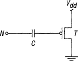
图1A为图1B浮栅MOSFET的漏极电流对比控制栅电源电压的曲线图。FIG. 1A is a graph of drain current versus control gate supply voltage for the floating gate MOSFET of FIG. 1B.
图2A为根据本发明实施例的装置的正视横截面图。Figure 2A is a front cross-sectional view of a device according to an embodiment of the invention.
图2B为图2A装置的MOS能带图。Fig. 2B is a MOS energy band diagram of the device of Fig. 2A.
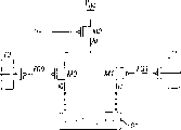
图3为根据本发明实施例的存储器的电示意图。pFET M2用于通过信号“偏压”来设定该差分对偏流,而浮栅pFET M0和M1充当存储装置。短路的pFET T0和T1用以从浮栅中除去电荷从而和/或充当控制栅。如所属领域的技术人员将显而易见的是,可使用短路的nFET来替代地建构T0和T1。FIG. 3 is an electrical schematic diagram of a memory according to an embodiment of the present invention. The pFET M2 is used to set the differential pair bias current through the signal "bias", while the floating gate pFETs M0 and M1 act as memory devices. The shorted pFETs T0 and T1 are used to remove charge from the floating gate and/or act as a control gate. As will be apparent to those skilled in the art, T0 and T1 can be constructed instead using shorted nFETs.
图4为与栅极到漏极电压对比注入效率的曲线图,其中注入效率定义为栅电流除以源电流。Figure 4 is a graph of injection efficiency versus gate-to-drain voltage, where injection efficiency is defined as gate current divided by source current.
图5A为根据本发明一个替代实施例的存储器的电示意图,其包含一个无穿隧接合(tunneling junction)的差分存储器。可使用UV光或所属技术领域人员熟知的其它技术来擦除浮栅,且可使用注入对存储器进行一次编程。5A is an electrical schematic diagram of a memory according to an alternate embodiment of the present invention, which includes a differential memory without tunneling junctions. The floating gate can be erased using UV light or other techniques known to those skilled in the art, and the memory can be programmed once using the implant.
图5B为根据图5A电路的替代实施例的存储器电示意图。5B is an electrical schematic diagram of a memory according to an alternative embodiment of the circuit of FIG. 5A.
图6A为差分存储器电示意图,其具有选择晶体管(select transistor)以判定存储器之哪一侧将经受本发明实施例的注入。FIG. 6A is an electrical schematic diagram of a differential memory with select transistors to determine which side of the memory is to be implanted according to an embodiment of the present invention.
图6B为根据图6A存储器的替代实施例的存储器电示意图,其包括一个根据本发明实施例的行选择开关。6B is an electrical schematic diagram of a memory according to an alternative embodiment of the memory of FIG. 6A including a row select switch according to an embodiment of the present invention.
图7为耦合到pFET电流源的差分存储器电路的电示意图,其具有在此情况下以根据本发明实施例的nFET建构的选择晶体管(S0、S1)(在此有时称作“序列选择开关”)。7 is an electrical schematic diagram of a differential memory circuit coupled to a pFET current source, with select transistors (S0, S1) (sometimes referred to herein as "sequence select switches") constructed in this case with nFETs according to embodiments of the invention. ).
图8为差分存储器电路的电示意图,其中在根据本发明实施例,电流被控制在浮栅注入晶体管的漏极。因为存在两个单独的电流控制,所以可在M0和M1中分别控制注入。8 is an electrical schematic diagram of a differential memory circuit in which current is controlled at the drain of a floating gate injection transistor in accordance with an embodiment of the present invention. Because there are two separate current controls, injection can be controlled separately in M0 and M1.
图9为根据本发明另一实施例的图8差分存储器电路的电示意图。在此版本中,对节点偏差0或节点偏差1施加正偏压并对其它节点施加0V将写入所述存储器。FIG. 9 is an electrical schematic diagram of the differential memory circuit of FIG. 8 according to another embodiment of the present invention. In this version, applying a positive bias to
图10为根据本发明实施例的存储器电路的电示意图,其包括与每一浮栅有关的pFET读取晶体管。10 is an electrical schematic diagram of a memory circuit including a pFET read transistor associated with each floating gate, according to an embodiment of the invention.
图11为根据类似图10的本发明实施例的存储器电路的电示意图,但是其包括行选择晶体管(M0、M1)以从差分读出放大器(sense amplifier)选择性隔离个别存储位置。Figure 11 is an electrical schematic diagram of a memory circuit according to an embodiment of the invention similar to Figure 10, but including row select transistors (MO, Ml) to selectively isolate individual memory locations from differential sense amplifiers.
图12为根据本发明实施例的图11方框12内所含有的电路的替代部分的电示意图。12 is an electrical schematic diagram of an alternative portion of the circuitry contained within block 12 of FIG. 11 in accordance with an embodiment of the present invention.
图13为建构双向穿隧的本发明实施例的电示意图。FIG. 13 is an electrical schematic diagram of an embodiment of the present invention for constructing bidirectional tunneling.
图14为基于图13的本发明替代实施例的电示意图。在此版本中,通过电子注入写入存储器,并且pFET读取晶体管与每一浮栅相关联。电容性耦合的控制栅输入节点促进本文描述的边界读取(margin read)和写干扰减轻处理。FIG. 14 is an electrical schematic diagram of an alternative embodiment of the invention based on FIG. 13 . In this version, the memory is written by electron injection, and a pFET read transistor is associated with each floating gate. Capacitively coupled control gate input nodes facilitate the margin read and write disturb mitigation processes described herein.
图15为本发明实施例的电示意图,其中一半的差分存储位置由一行存储器阵列的所有存储位置(memory location)共享的。此实施例对差分存储器的内存条(memory bank)尤其有用。15 is an electrical schematic diagram of an embodiment of the present invention, wherein half of the differential storage locations are shared by all storage locations (memory locations) of a row of memory arrays. This embodiment is especially useful for differential memory memory banks.
图16为通过添加一对浮栅晶体管(M2、M3)以监视穿隧处理的结束来修改图14版本的本发明实施例的电示意图。Figure 16 is an electrical schematic diagram of the embodiment of the invention modified from the version of Figure 14 by adding a pair of floating gate transistors (M2, M3) to monitor the end of the tunneling process.
图17为本发明实施例的电示意图,其使用反馈以在穿隧期间审慎地少量注入存储器,来预防存储器浮栅的过穿隧问题。FIG. 17 is an electrical schematic diagram of an embodiment of the present invention that uses feedback to deliberately inject a small amount of memory during tunneling to prevent over-tunneling of the floating gate of the memory.
图18为展现图17存储器简化的本发明实施例的电示意图。所述Read not信号用于将存储器配置为读取模式。FIG. 18 is an electrical schematic diagram showing a simplified embodiment of the invention of the memory of FIG. 17. FIG. The Read not signal is used to configure the memory into a read mode.
图19和20为本发明实施例的电示意图,其说明了可在所述注入晶体管的漏极侧控制存储器电流。图20的实施例具有控制所述写入和读取电流的明确的nFET电流槽(current sink)M0。19 and 20 are electrical schematic diagrams of embodiments of the present invention illustrating that memory current can be controlled at the drain side of the injection transistor. The embodiment of Figure 20 has an explicit nFET current sink M0 that controls the write and read currents.
图21为根据本发明实施例的pFET穿隧接合装置的布局图。FIG. 21 is a layout diagram of a pFET tunnel bonding device according to an embodiment of the present invention.
图22为沿图21的线22-22截取的横截面图。22 is a cross-sectional view taken along line 22-22 of FIG. 21 .
图23为根据本发明实施例的n井整体(bulk)nFET穿隧接合装置的布局图。23 is a layout diagram of an n-well bulk nFET tunnel bonding device according to an embodiment of the present invention.
图24为根据本发明实施例的MOSCAP型穿隧接合装置的横截面图。FIG. 24 is a cross-sectional view of a MOSCAP-type tunnel bonding device according to an embodiment of the present invention.
图25为根据本发明实施例的差分存储器的电示意图。FIG. 25 is an electrical schematic diagram of a differential memory according to an embodiment of the present invention.
图26为根据本发明另一实施例的替代差分存储器的电示意图。FIG. 26 is an electrical schematic diagram of an alternative differential memory according to another embodiment of the present invention.
图27为另一个差分存储器的电示意图。Fig. 27 is an electrical schematic diagram of another differential memory.
图28为差分存储器的电示意图,其具有使其不同侧经独立写入的能力。Figure 28 is an electrical schematic diagram of a differential memory with the ability to have its different sides independently written.
图29为另一替代差分存储器的电示意图。Figure 29 is an electrical schematic diagram of another alternative differential memory.
图30为另一个替代差分存储器的电示意图。Figure 30 is an electrical schematic diagram of another alternative differential memory.
图31为另一个替代差分存储器的电示意图。Figure 31 is an electrical schematic diagram of another alternative differential memory.
图32为另一个替代差分存储器的电示意图。Figure 32 is an electrical schematic diagram of another alternative differential memory.
图33为另一个替代差分存储器的电示意图。Figure 33 is an electrical schematic diagram of another alternative differential memory.
图34为用于说明边界读取的第一方法的另一个替代差分存储器的电示意图。Figure 34 is an electrical schematic diagram of another alternative differential memory for illustrating the first method of boundary read.
图35为用于说明边界读取的第二方法的另一个替代差分存储器的电示意图。FIG. 35 is an electrical schematic diagram of another alternative differential memory used to illustrate the second method of boundary read.
图36为如那些本发明所涵盖的存储器的写入电流和写干扰电流对比写入电压的曲线图。36 is a graph of write current and write disturb current versus write voltage for a memory such as those encompassed by the present invention.
图37为设计用以降低写干扰的经修改的存储器的电示意图。Figure 37 is an electrical schematic diagram of a modified memory designed to reduce write disturb.
图38、39和40为具有各种类型差分存储器的差分存储器阵列的替代建构。Figures 38, 39 and 40 are alternative constructions of differential memory arrays with various types of differential memory.
图41和42为外部注入电路的替代建构,其用以分开以相对高的浮栅制造的存储器,其反而可能阻止电子注入到浮栅上。Figures 41 and 42 are alternative configurations of external injection circuits used to separate memories fabricated with relatively tall floating gates, which would otherwise prevent electrons from being injected onto the floating gates.
图43为说明根据本发明实施例存储器的阵列布局图。FIG. 43 is a diagram illustrating an array layout of a memory according to an embodiment of the present invention.
图44为根据本发明实施例的示范性写入电路的电示意图。44 is an electrical schematic diagram of an exemplary write circuit according to an embodiment of the present invention.
图45为根据现有技术的示范性差分读出放大器电路的电示意图。45 is an electrical schematic diagram of an exemplary differential sense amplifier circuit according to the prior art.
图46为根据现有技术UV可擦除的视窗存储装置的正视横截面图。Figure 46 is a front cross-sectional view of a UV-erasable window memory device according to the prior art.
具体实施方式Detailed ways
本文以差分浮栅非挥发性存储器描述本发明的实施例。所属领域的技术人员将了解本发明的下列详细说明仅是说明性的,并且无意以任何方式限制。受益于此揭示内容的所属领域技术人员容易明了本发明的其它实施例。现在将详细参照如在本发明随附图式中所说明的本发明的建构。贯穿图式和下列详细说明使用相同的参考代号以指代相同或类似部分。Embodiments of the invention are described herein in terms of a differential floating gate non-volatile memory. Those skilled in the art will appreciate that the following detailed description of the invention is illustrative only and is not intended to be limiting in any way. Other embodiments of the invention will be readily apparent to those skilled in the art having the benefit of this disclosure. Reference will now be made in detail to constructions of the invention as illustrated in the accompanying drawings of the invention. The same reference numbers are used throughout the drawings and the following detailed description to refer to the same or like parts.
为清晰起见,并不在此展示和描述所有的所述建构的常规特征。当然应了解在任何所述实际建构的开发中,必须判定无数特定建构以便达到开发商的特定目标,诸如顺应应用和商业相关的约束,并且这些特定目标会依各建构和各开发商而改变。此外,应了解所述开发工作可能复杂而耗时,但对于受益于此揭示内容的所属领域技术人员其会成为工程的常规任务。In the interest of clarity, not all of the routine features of the described constructions are shown and described herein. It should of course be understood that in the development of any such actual configuration, a myriad of specific configurations must be determined in order to achieve the developer's specific goals, such as compliance with application and business-related constraints, and that these specific goals will vary from configuration to configuration and from developer to developer. Furthermore, it should be understood that such development might be complex and time consuming, but would nevertheless become a routine undertaking of engineering for those skilled in the art having the benefit of this disclosure.
本发明一般用于非挥发性存储器,且具有如在嵌入式CMOS应用中可能发现的低密度嵌入式非挥发性存储器的特别应用。所述嵌入式CMOS应用包括(但不限于)存储:(1)芯片序列号(即,芯片标签);(2)ASIC(应用特定集成电路)中的配置信息;(3)射频识别(RFID)集成电路中的产品、封装和/或资产数据;(4)嵌入式微控制器的编码或数据;(5)模拟微调信息;(6)FPGA配置信息;和(7)如所属领域技术人员明了的许多其它应用。与常规的基于nFET的非挥发性存储器相比,使用pFET具有至少以下优点:电荷泵功率降低、编程/擦除循环持久性(由于氧化磨损减少)增加,和在逻辑CMOS制程中可用(由于存储器泄漏减少和事实上存储器仅使用nFET和pFET)。The present invention is generally applicable to non-volatile memory, and has particular application to low density embedded non-volatile memory as might be found in embedded CMOS applications. The embedded CMOS applications include (but are not limited to) storing: (1) chip serial number (ie, chip tag); (2) configuration information in an ASIC (application specific integrated circuit); (3) radio frequency identification (RFID) product, package, and/or asset data in integrated circuits; (4) code or data for embedded microcontrollers; (5) analog trimming information; (6) FPGA configuration information; and (7) as would be apparent to those skilled in the art Many other applications. Compared to conventional nFET-based non-volatile memories, the use of pFETs has at least the following advantages: reduced charge pump power, increased program/erase cycle endurance (due to reduced oxide wear), and availability in logic CMOS processes (due to memory Leakage reduction and the fact that memory only uses nFETs and pFETs).
任何可重新编程的NVM技术必须符合两个关键要求:(1)持久性和(2)保持性。持久性指的是擦除/写入循环的次数(NVM理想上可具有无限次读取循环)。保持性指的是存储器存储时间。在过去的二十年中,闪存和EEPROM技术的以致使产生一套商业上可接受的NVM设计标准。标准CMOS制程中的任何设计应该符合这些相同标准。所述两项标准是10年的保持性和10,000次(最小)的擦除/写入循环。Any reprogrammable NVM technology must meet two key requirements: (1) persistence and (2) retention. Endurance refers to the number of erase/write cycles (NVM can ideally have infinite read cycles). Retentivity refers to memory storage time. Over the past two decades, the evolution of flash memory and EEPROM technologies has resulted in a set of commercially acceptable NVM design standards. Any design in a standard CMOS process should meet these same criteria. The two criteria are 10 years retention and 10,000 (minimum) erase/write cycles.
NVM装置通过改变晶体管或其它电路元件的物理属性来存储信息。在浮栅存储器(如,闪存或EEPROM)的情况下,所述物理属性是存储在硅MOSFET(金属氧化半导体场效晶体管)的电隔离(浮动)栅上的电子量。所有的NVM装置磨损,意味着在一定次数的擦除/写入循环后,所述存储器将不再符合其10年保持性的要求。在浮栅存储器的情况下,因为移动电子通过围绕电隔离栅的氧化绝缘体总是损害该绝缘氧化物。NVM devices store information by changing the physical properties of transistors or other circuit elements. In the case of floating gate memory (eg, flash memory or EEPROM), the physical property is the amount of electrons stored on the electrically isolated (floating) gate of a silicon MOSFET (Metal Oxide Semiconductor Field Effect Transistor). All NVM devices wear out, meaning that after a certain number of erase/write cycles, the memory no longer meets its 10-year retention requirements. In the case of floating gate memories, the insulating oxide is always damaged by moving electrons through the oxidized insulator surrounding the electrical isolation barrier.
浮栅存储器技术是以硅MOSFET的浮栅上的电子来存储信息。从浮栅添加或除去电子会改变MOSFET的阈值电压。图1A是用于图1B的浮栅MOSFET的漏极电流对比控制栅电源电压的曲线图。为了读取存储器,要测量浮栅MOSFET的通道电流。如观察图1A的左侧曲线,那么所存储的存储器是逻辑“1”;如果观察图1A的右侧曲线,那么所存储的存储器是逻辑“0”,或反过来也如此。在不存在控制栅时,浮栅的电压确定其相关晶体管的状态。对于pFET,低浮栅电压意味着晶体管更多为“on”(即,较高的源极-漏极电流),然而高浮栅电压意味着晶体管更多为“off”(即,较低的源极-漏极电流)。可基于浮栅晶体管的相对on/off状态而读取逻辑“1”或逻辑“0”。Floating-gate memory technology uses electrons on the floating gate of a silicon MOSFET to store information. Adding or removing electrons from the floating gate changes the threshold voltage of the MOSFET. 1A is a graph of drain current versus control gate supply voltage for the floating gate MOSFET of FIG. 1B. To read the memory, the channel current of the floating gate MOSFET is measured. If one looks at the left curve of FIG. 1A, then the stored memory is a logic "1"; if one looks at the right curve of Fig. 1A, then the stored memory is a logic "0", or vice versa. In the absence of the control gate, the voltage of the floating gate determines the state of its associated transistor. For a pFET, a low floating gate voltage means the transistor is more "on" (ie, higher source-drain current), whereas a high floating gate voltage means the transistor is more "off" (ie, lower source-drain current). A logical "1" or a logical "0" can be read based on the relative on/off states of the floating gate transistors.
NVM设计人员可使用n通道或p通道浮栅MOSFET作为存储器晶体管。自从20世纪80年代早期已使用n通道MOSFET,这是因为尺寸较小并且存在将nFET通道电子注入到浮栅上的直接方法。这个选择启动高度经修改的CMOS制程的高密度闪存和EEPROM。然而,在逻辑CMOS中,情况相反——pFET大大优于nFET,因为与nFET NVM相比pFET NVM具有较好的保持性,并且与nFET NVM相比pFET NVM允许更多的擦除/写入循环。NVM designers can use n-channel or p-channel floating-gate MOSFETs as memory transistors. n-channel MOSFETs have been used since the early 1980s because of the smaller size and the existence of a direct method of injecting nFET channel electrons onto the floating gate. This option enables high-density flash and EEPROM in highly modified CMOS processes. In logic CMOS, however, the opposite is true - pFETs are vastly better than nFETs because pFET NVMs have better retention compared to nFET NVMs, and pFET NVMs allow more erase/write cycles than nFET NVMs .
当然,使用pFET NVM也存在缺点。在专用制程中发现与nFET NVM相比pFET NVM具有较大尺寸,并且趋向具有较长的写入时间。对于小存储器(即,那些小于或等于大约60kbits的存储器),保持性和持久性利益和零制程遮罩增加显著胜过这些缺点。Of course, there are downsides to using pFET NVM. It is found that pFET NVM has a larger size compared to nFET NVM in a dedicated process and tends to have a longer write time. For small memories (ie, those less than or equal to about 60 kbits), the retention and persistence benefits and zero process mask increase significantly outweigh these disadvantages.
图2A是用于根据本发明实施例的装置正视横截面图。图2B是用于图2A的装置的MOS能带图。图2A和2B说明pFET NVM为什么具有与nFETNVM相比较好的保持性。装置物理性展示对于从pFET的电子泄漏的能障是4.16eV,然而对于nFET仅为3.04eV。这个差别意味着在相同的氧化物厚度下,pFET存储器可以其较高的能障展现出显著小于nFET存储器的穿过栅氧化物的电子穿隧现象。在专用CMOS制程中,这个差异并没有实际影响,因为制程工程师仅需加厚所述栅氧化,直到存储器具有10年的保持性。所有目前商用基于nFET的NVM都使用80或更厚的氧化物。不幸地是,在现代逻辑CMOS中并不存在80的氧化物(0.35μm和更小的制程线宽)。从而,在逻辑CMOS中以70或较薄的栅氧化物构造的nFET NVM在正常的制程变化和温度变化上根本无法满足10年保持性的要求。解决方案是使用pFET NVM。如在现代双栅氧化物CMOS制程中可用的70pFET具有与专用制程中的82nFET相同的数据保持性。简而言之,保持性对于NVM很关键,并且在目前技术逻辑CMOS中pFET具有10年的保持性,然而nFET没有。Figure 2A is a front cross-sectional view of a device according to an embodiment of the present invention. Figure 2B is a MOS energy band diagram for the device of Figure 2A. Figures 2A and 2B illustrate why pFET NVM has better retention than nFET NVM. The device physically exhibits an energy barrier of 4.16 eV for electron leakage from the pFET, whereas only 3.04 eV for the nFET. This difference means that at the same oxide thickness, the pFET memory can exhibit significantly less electron tunneling through the gate oxide with its higher energy barrier than the nFET memory. In a dedicated CMOS process, this difference has no real impact, because process engineers only need to thicken the gate oxide until the memory has 10-year retention. All current commercial nFET-based NVMs use 80 Å or thicker oxides. Unfortunately, 80 Å oxide (0.35 μm and smaller process linewidths) does not exist in modern logic CMOS. Thus, an nFET NVM constructed in logic CMOS with a gate oxide of 70 Å or thinner simply cannot meet the 10-year retention requirement under normal process variations and temperature variations. The solution is to use pFET NVM. A 70 Å pFET as available in a modern dual gate oxide CMOS process has the same data retention as an 82 Å nFET in a dedicated process. In short, retention is critical for NVM and in current technology logic CMOS pFETs have 10 year retention whereas nFETs do not.
Diorio等人的题目为“Hole Impact Ionization Mechanism for Hot E1ectronInjection and Four Terminal pFET Semiconductor Structure for Long-TermLearning”的美国专利第5,990,512号描述了用于向并从浮栅pFET的栅传送电荷的方法。本发明的某些实施例使用浮栅pFET作为存储器存储晶体管,而512专利中所描述的撞击离子化热电子注入(IHEI)和穿隧方法用于写入存储器。本发明其它实施例运用直接穿隧代替IHEI。因为IHEI和穿隧并不要求特定装置制程,所以可使用与制造标准数字逻辑晶体管相同的IC制程建造浮栅装置。U.S. Patent No. 5,990,512 to Diorio et al., entitled "Hole Impact Ionization Mechanism for Hot Electron Injection and Four Terminal pFET Semiconductor Structure for Long-Term Learning," describes a method for transferring charge to and from the gate of a floating-gate pFET. Certain embodiments of the present invention use floating gate pFETs as memory storage transistors, and the impact ionization hot electron injection (IHEI) and tunneling methods described in the '512 patent are used to write memory. Other embodiments of the invention use direct tunneling instead of IHEI. Because IHEI and tunneling do not require specific device processes, floating-gate devices can be built using the same IC processes used to fabricate standard digital logic transistors.
差分存储器技术Differential Memory Technology
通过采用差分存储器,而不是标准单端存储器,使根据本发明制作的存储器展现出增加的读取速度、降低的读取电流和功率消耗、降低的穿隧和注入效率的变化的敏感度、宽松的芯片上电流和电压参考的精确度的要求,以及降低的温度和电源电压敏感度。从而,使用差分式的基于pFET的存储器的组合方法可启动逻辑CMOS中的NVM。By employing differential memories, rather than standard single-ended memories, memories fabricated in accordance with the present invention exhibit increased read speed, reduced read current and power consumption, reduced sensitivity to changes in tunneling and injection efficiencies, relaxed Accuracy requirements for on-chip current and voltage references, as well as reduced temperature and supply voltage sensitivity. Thus, a combined approach using differential pFET-based memory enables NVM in logic CMOS.
图3是根据本发明实施例的存储器的电示意图。pFET M2用以通过信号“偏压”来设定差分对偏流Ib,且浮栅pFET M0和M1充当存储装置。短路的pFET T0和T1用以从浮栅除去电子和/或充当控制栅。如所属领域的技术人员将显而易见的,可使用短路的nFET或MOSCAP替代地建构T0和T1。(控制栅是电容器或电容性耦合到浮栅的节点。根据本发明,所述控制栅可以建构为电容器或短路的pFET等,而无需将另一层添加到半导体晶片)可通过存储在两个浮栅FG0和FG1上,而不是如基于nFET的NVM中常见的单一存储器元件的开-关状态上的电荷差,来确定差分存储器的逻辑状态。无论存储器元件存储的是逻辑0或逻辑1,两个晶体管都具有反相通道。常规差分读出放大器电路D1分别地读出M0与M1的漏极电流I0和I1,来确定存储器的状态。3 is an electrical schematic diagram of a memory according to an embodiment of the present invention. The pFET M2 is used to set the differential pair bias current Ib by the signal "bias", and the floating gate pFETs M0 and M1 act as memory devices. Shorted pFETs T0 and T1 are used to remove electrons from the floating gate and/or act as a control gate. T0 and T1 may alternatively be constructed using shorted nFETs or MOSCAPs, as will be apparent to those skilled in the art. (The control gate is a capacitor or a node that is capacitively coupled to a floating gate. According to the invention, the control gate can be constructed as a capacitor or a shorted pFET, etc. without adding another layer to the semiconductor wafer) The difference in charge on the floating gates FG0 and FG1 , rather than the on-off state of a single memory element as is common in nFET-based NVM, determines the logic state of the differential memory. Both transistors have inverting channels whether the memory element is storing a
基本存储器元件的擦除循环可以如下运作。可以通过使用Fowler-Nordheim穿隧以从两个浮栅除去电子的方式来擦除差分存储器。根据本发明的一个实施例,这可以通过使两者穿隧接合(T0和T1)到大约10V而完成。为了在pFET浮栅晶体管隧道到完全关闭状态之前停止所述擦除处理,所以将在擦除处理期间以常规方式监视漏极电流(I0和I1)。一旦特别存储器元件的漏极电流达到预定最小值后(如,根据本发明一个实施例的约10nA),穿隧完成(TunDone)信号就以常规方式产生。这个信号可以用来停止在那个浮栅上或在浮栅的区块上的穿隧处理。这个反馈处理确保当擦除时没有浮栅晶体管被完全关闭。The erase cycle of a basic memory element may work as follows. Differential memory can be erased by using Fowler-Nordheim tunneling to remove electrons from both floating gates. According to one embodiment of the invention, this can be done by tunneling the two junctions (T0 and T1) to about 10V. In order to stop the erase process before the pFET floating gate transistor tunnels to a fully off state, the drain currents (I0 and I1 ) will be monitored during the erase process in a conventional manner. Once the drain current of a particular memory element reaches a predetermined minimum value (eg, about 10 nA according to one embodiment of the present invention), a tunnel complete (TunDone) signal is generated in a conventional manner. This signal can be used to stop tunneling on that floating gate or on blocks of floating gates. This feedback process ensures that no floating gate transistor is completely turned off when erasing.
基本存储器元件的编程循环可以如下运作。为了将逻辑1编程到存储位置,可以使用晶体管M2对存储器元件施加偏流,而同时在晶体管M1上施加相对大的漏极到源极电压(通过向M1漏极施加低或负电压)。0.18μmCMOS制程中的典型值是Vdd=1.8V并且V_M1drain=-3.3V。晶体管M2和M1导电,并且使用如美国专利第5,990,512号所论述的IHEI制程将电子注入到浮栅FG1上。随后进行相同程序以写入逻辑0,除了是注入晶体管M0而不是M1以外。A programming loop for a basic memory element may work as follows. To program a logic one into a memory location, transistor M2 can be used to bias the memory element while simultaneously applying a relatively large drain-to-source voltage across transistor M1 (by applying a low or negative voltage to the M1 drain). Typical values in a 0.18 μm CMOS process are Vdd = 1.8V and V_M1 drain = -3.3V. Transistors M2 and M1 conduct and inject electrons onto floating gate FG1 using an IHEI process as discussed in US Patent No. 5,990,512. The same procedure is followed to write a
所述注入制程是自限性的,意味着当电子注入到浮栅上时,晶体管自身会停止所述注入制程。不像nFET、pFET会自限其IHEI电流,因为注入会引起其浮栅电压降低。随着栅极电压降落,注入晶体管的漏极到栅极电压也会降低。因为IHEI会随着漏极到栅极电压的降低而按指数规律地降低(如,图4所说明的,其为栅极电流/电源电流对栅极到漏极电压的曲线图),所述晶体管自身停止IHEI制程。The injection process is self-limiting, meaning that when electrons are injected onto the floating gate, the transistor itself stops the injection process. Unlike nFETs, pFETs self-limit their IHEI current because injection causes their floating gate voltage to drop. As the gate voltage drops, the drain-to-gate voltage of the injection transistor also decreases. Because IHEI decreases exponentially with decreasing drain-to-gate voltage (as illustrated in Figure 4, which is a graph of gate current/supply current versus gate-to-drain voltage), the The transistor itself stops the IHEI process.
或者,所属领域的技术人员现将认识到也可以创建一个可以用于终止注入制程的发信号电路,如,通过当注入晶体管的浮栅触达到预定电压时,通过晶体管M2来阻挡电流。Alternatively, those skilled in the art will now recognize that it is also possible to create a signaling circuit that can be used to terminate the injection process, eg, by blocking current through transistor M2 when the floating gate of the injection transistor touches a predetermined voltage.
基本差分存储器元件的读取循环可以如下运作。为了读取差分存储器元件的内容,首先使用晶体管M2向存储器元件施加偏流。读取根据区别在两个半个差分存储器元件之间的较为导电路径的原理而操作。如果FG0具有比FG1低的电压,那么M0将会更为导电,并且大部分的偏流将按I0而穿过。如果FG1具有比FG0低的电压,那么保持互补情况。接着,常规差分读出放大器通过比较I0和I1来判定存储器元件是否保持逻辑1或逻辑0。因为所述存储器为差分的,所以当读取存储器时,可以在晶体管M2内使用任意小的偏流。从而,在读取操作期间,存储器可以使用任意低的功率。穿隧接合A read cycle for a basic differential memory element may work as follows. To read the contents of a differential memory element, a bias current is first applied to the memory element using transistor M2. Reading operates on the principle of distinguishing a more conductive path between the two halves of a differential memory element. If FG0 has a lower voltage than FG1, then M0 will be more conductive and most of the bias current will flow as I0. If FG1 has a lower voltage than FG0, then the complementary situation remains. Next, a conventional differential sense amplifier determines whether the memory element holds a
图5A是本发明的替代实施例的存储器的电示意图,其中包含无穿隧接合的差分存储器,以从浮栅FG0和FG1除去电子。在此,可通过使用透过含有芯片C上的装置的封装P中的适当视窗W的诸如展示在浮栅上的UV光的电磁辐射,或所属领域的技术人员熟知的其它技术,根据本实施例来擦除封装P(如图46说明)的芯片C上的浮栅FG0和FG1,并且通过使用由电流源、电阻器、FET或电压源(本文通称为电流源)供电的注入来对存储器进行一次编程。以此方式可以节省与穿隧接合相关的布局面积。除去穿隧接合的选择适用于所有本发明的实施例,而将穿隧接合放入基板的相同或单独的n井内的选择也同样适用。如果穿隧接合形成在单独n井中,那么可以为擦除的目的而选择存储器的单一节点(即,单侧)。如果穿隧接合形成在相同的n井内,那么可以保留晶粒区域,并且同时擦除差分存储器的两侧。特别实施例中使用的精确构造将取决于设计人员。图5B说明了图5A存储器的替代实施例,其包括分别由选择线路Sel_0、Sel_1控制的选择晶体管S0、S1。在这个版本中并没有提供穿隧接合。5A is an electrical schematic diagram of a memory of an alternative embodiment of the present invention, including a differential memory without tunnel junctions to remove electrons from floating gates FG0 and FG1. Here, by using electromagnetic radiation such as UV light exhibited on a floating gate through a suitable window W in a package P containing a device on a chip C, or other techniques well known to those skilled in the art, the For example to erase floating gates FG0 and FG1 on chip C in package P (as illustrated in FIG. 46 ) and to power the memory by using an injection powered by a current source, a resistor, a FET, or a voltage source (collectively referred to herein as a current source). Do a programming. In this way layout area associated with tunnel bonding can be saved. The option of removing the tunneling junction applies to all embodiments of the invention, as does the option of placing the tunneling junction in the same or a separate n-well of the substrate. If the tunnel junctions are formed in a single n-well, then a single node (ie, a single side) of the memory can be selected for erase purposes. If the tunnel junctions are formed in the same n-well, then the die area can be preserved and both sides of the differential memory can be erased simultaneously. The precise configuration used in a particular embodiment will be up to the designer. FIG. 5B illustrates an alternative embodiment of the memory of FIG. 5A comprising select transistors S0 , S1 controlled by select lines Sel_0 , Sel_1 , respectively. Tunnel bonding is not provided in this version.
本文描述的装置可以为可擦除或可一次编程的。对于可一次编程的装置,并不要求穿隧接合(尽管其可包括作为一个设计选择)。那些要求擦除的本发明的实施例可以建构穿隧接合以使电子穿隧离开浮栅。可以许多不同方式建构穿隧接合。在一个实施例中,将单独的n井远离浮栅晶体管所位于的n井而放置。所述浮栅晶体管是一个pFET,其可用于IHEI、直接穿隧或另外用于跨越绝缘体将电子移动到浮栅的类似制程。根据本实施例,将浮栅放置在两个n井之间。所述穿隧接合可以是:(1)一个MOSCAP,诸如如图24中所展示的元件124,其建构为安置在n井中的n+区;(2)一个短路的nFET(具有相互连接的漏极和源极);(3)一个短路的pFET(具有相互连接的漏极、源极和井接触);或如现将对所属领域的技术人员显而易见的其它排置方式。参见图2A关于根据本发明一个实施例的存储器的一般布局。The devices described herein can be erasable or one-time programmable. For one-time programmable devices, tunnel bonding is not required (although it may be included as a design choice). Embodiments of the present invention that require erasure can implement tunnel junctions to allow electrons to tunnel away from the floating gate. Tunneling junctions can be constructed in many different ways. In one embodiment, a separate n-well is placed away from the n-well where the floating gate transistor is located. The floating gate transistor is a pFET that can be used for IHEI, direct tunneling, or otherwise similar processes that move electrons across an insulator to the floating gate. According to this embodiment, the floating gate is placed between two n-wells. The tunnel junction can be: (1) a MOSCAP, such as
现转向图21和22,图中说明了一个pFET穿隧接合。图21为pFET穿隧接合的布局(上)图,并且图22为沿图21的线22-22截取的横截面图。如可以看到,所述装置安置在n井100中,其中n井安置在基板102中。pFET穿隧接合装置104包括n+井接触区106和源极p+区108以及漏极p+区110,在可能的地方,所有这些都可以被页面内的逐个存储器元件所共享。浮栅112座落于形成在源极和漏极之间通道上,并且通过诸如二氧化硅的介电层114与通道分离。井接触、源极和漏极通过导体116而共同短路,所述导体116由任何适当的导电材料构成。Turning now to Figures 21 and 22, a pFET tunnel junction is illustrated. 21 is a layout (top) view of a pFET tunnel junction, and FIG. 22 is a cross-sectional view taken along line 22-22 of FIG. As can be seen, the device is arranged in an n-well 100 , wherein the n-well is arranged in a
现转向图23,在所述横截面图中说明了nFET穿隧接合装置118。在本实施例里,将n井100安置在p基板102中。在n井100内是一对构成晶体管源极和漏极的n+区120和122。这些如上所述的通过导体116而彼此短路。如上所述,浮栅112座落于形成在源极和漏极之间的通道上,并且通过诸如二氧化硅的介电层114与通道分离。Turning now to FIG. 23, an nFET
现转向图24,在横截面图中说明了MOSCAP穿隧接合装置124。在本实施例中,将n井100安置在p基板102中。在n井100内是耦合到导体116的n+区126。本装置的其余细节如上文所述。Turning now to FIG. 24, the MOSCAP
到差分存储器一侧的限制性注入Restricted injection into the differential memory side
图6A为具有选择晶体管的差分存储器电示意图,所述选择晶体管判定存储器的哪一侧经受根据本发明实施例的注入。图6A的存储器超过图3存储器的优点,在于两个注入晶体管M0、M1的漏极在注入期间可被降低,并且可以通过施加选择信号到其对应的选择线路Sel_0、Sel_1,来启动对应的选择晶体管S0、S1,来选择一侧用于写入。可以将这个差分对的输入节点X连接到如图3中的偏压晶体管或任何其它类型的可选电流源电路。如在本文所展示的每一个实施例中,所述输入节点X可以是安置在实际存储器内的电流源,或通向安置在其它地方的另一电流源的导体。例如在阵列列中的存储器元件之中共享电流源可节省布局面积,但是由于在共享节点处的增加的电容可能降低速度。如果合乎设计,也可以通过使用适当的选择晶体管将电流引导到作为适当的节点X,而对于读出/写入操作之一使用元件内电流源,对于其它操作使用元件外电流源。在权利要求书中,术语“电流源”意思是表达可以从其中汲取电流的节点的概念,因而,例如,如果在存储器元件内存在供应有电流的节点,那么所述节点可以为电流源,即使其是由在存储器元件自身外部的晶体管供应电流也是如此。Figure 6A is an electrical schematic diagram of a differential memory with select transistors that determine which side of the memory is subject to an implant according to an embodiment of the invention. The advantage of the memory of FIG. 6A over the memory of FIG. 3 is that the drains of the two injection transistors M0, M1 can be lowered during injection and the corresponding selection can be activated by applying a selection signal to its corresponding selection line Sel_0, Sel_1. Transistors S0, S1, to select one side for writing. The input node X of this differential pair can be connected to a bias transistor as in Figure 3 or any other type of optional current source circuit. As in each of the embodiments presented herein, the input node X may be a current source disposed within the actual memory, or a conductor to another current source disposed elsewhere. Sharing current sources, eg, among memory elements in an array column may save layout area, but may reduce speed due to increased capacitance at the shared nodes. It is also possible, if desired, to use an appropriate select transistor to direct the current to the appropriate node X, using an internal current source for one of the read/write operations and an external current source for the other. In the claims, the term "current source" is meant to express the concept of a node from which current can be drawn, thus, for example, if within a memory element there is a node to which current is supplied, said node can be a current source even if The same is true for supplying current by transistors external to the memory element itself.
行选择line selection
现转向图6B,将行选择晶体管M2添加到图6A的基本构造上。耦合到M2栅极的Row_Sel线路的控制电流源C1是否耦合到节点X。因为多达一半的晶体管使其源极/漏极连接到节点,所以以此方式通过外部(列)电流源所观察到的电容降低。由于降低的电容,所以这种方法提供了较快的读取和写入。Turning now to FIG. 6B, a row select transistor M2 is added to the basic configuration of FIG. 6A. The Row_Sel line coupled to the gate of M2 controls whether current source C1 is coupled to node X. Since as many as half of the transistors have their source/drain connected to a node, the capacitance observed by the external (column) current source is reduced in this way. This approach provides faster reads and writes due to the reduced capacitance.
图7为耦合到pFET电流源的差分存储器的电示意图,并且所述选择晶体管(S0、S1)根据本发明实施例与nFET一起建构。所述存储器通过将Vdd拉升(到大约5V)、通过设定其栅极电压到Vdd以开启选择晶体管(S0、S1)之一、并且通过设定其电压到接地以关闭另一个选择晶体管来进行编程。在“开”侧的浮栅晶体管(M0、M1)将经受IHEI,引起其栅极电压降落。在“关闭”侧的浮栅的晶体管(M0、M1)不具有任何通道电流,将其注入降低到可以忽略的级别,并且使其栅极电压仍然大致不变。Figure 7 is an electrical schematic diagram of a differential memory coupled to a pFET current source, and the select transistors (S0, S1 ) are constructed with nFETs according to an embodiment of the invention. The memory operates by pulling Vdd up (to about 5V), turning on one of the select transistors (S0, S1) by setting its gate voltage to Vdd, and turning off the other select transistor by setting its voltage to ground. for programming. The floating gate transistors (MO, M1 ) on the "on" side will experience IHEI, causing their gate voltage to drop. The floating-gate transistors (M0, M1) on the "off" side do not have any channel current, reducing their injection to negligible levels and leaving their gate voltages still roughly constant.
在替代实施例中,图7中的选择晶体管可以与pFET一起建构。还可以使用图7中的选择晶体管将阵列中的多个存储器元件从单一读出放大器D1分离。In an alternate embodiment, the select transistors in Figure 7 can be built with pFETs. The select transistors in FIG. 7 can also be used to separate multiple memory elements in the array from a single sense amplifier Dl.
图8为差分存储器电路的电示意图,其中在根据本发明实施例的浮栅注入晶体管的漏极处控制电流。因为存在两个单独的电流控制,所以在M0和M1中可用单独地控制IHEI。在本实施例中,电流“源”C0和C1可以是电流槽。电流“槽”可以沉降电流,而电流源可以供应电流。8 is an electrical schematic diagram of a differential memory circuit in which current is controlled at the drain of a floating gate injection transistor according to an embodiment of the invention. Because there are two separate current controls, IHEI can be controlled independently in M0 and M1. In this embodiment, current "sources" C0 and C1 may be current sinks. A current "sink" sinks current, and a current source supplies it.
图9为根据本发明实施例的图8版本电路的电示意图。在这个版本中,向偏差0或偏差1施加偏压,并且向其它信号施加0V将写入所述存储器。如果将偏差0设定为偏压电压并且将偏差1设定为0V,那么电流将流过M2和M0,引起M1中的IHEI并且降低FG0上的电压。在这种情况下,将没有电流流过M3和M1,因此在M1处的注入率会远小于在M0处的。而当将偏差1设定为偏压并且将偏差0设定为0V时,则会是相反情况。在读取期间,可将偏差0和偏差1两者设定为0V,来防止电流绕过读出放大器。FIG. 9 is an electrical schematic diagram of a version of the circuit of FIG. 8 according to an embodiment of the present invention. In this version, biasing either
关于图6A、6B、7、8和9的存储器的读取操作类似于图3所述的。The read operation of the memory with respect to FIGS. 6A , 6B, 7 , 8 and 9 is similar to that described for FIG. 3 .
通过将pFET读取晶体管(M2、M3)添加到如图10电路中的每个浮栅来分离编程和读取功能。图10为根据本发明实施例的示意图,其包括与每个浮栅相关的pFET读取晶体管。这项修改允许使晶体管的漏极电压(Vinj)低于接地,而在写入期间加速IHEI处理。这也会增加差分读出放大器设计上的弹性。The programming and reading functions are separated by adding pFET read transistors (M2, M3) to each floating gate as in the circuit of FIG. 10 . Figure 10 is a schematic diagram including a pFET read transistor associated with each floating gate, in accordance with an embodiment of the present invention. This modification allows the drain voltage (Vinj) of the transistor to be lower than ground, speeding up the IHEI process during writing. This also increases the flexibility in the design of the differential sense amplifier.
图11为类似图10的本发明实施例的示意图,但是其包括行选择晶体管(S2、S3,这些将通过“EN”信号选择性地激活),以从差分读出放大器隔离存储器元件。这项修改允许多个存储器元件共享单一差分读出放大器D1。视需要,选择晶体管(S2、S3)可以为nFET(如图中所示)或pFET。Figure 11 is a schematic diagram of an embodiment of the invention similar to Figure 10, but including row select transistors (S2, S3, these will be selectively activated by the "EN" signal) to isolate the memory elements from the differential sense amplifiers. This modification allows multiple memory elements to share a single differential sense amplifier D1. The select transistors (S2, S3) can be nFETs (as shown in the figure) or pFETs, as desired.
图12为根据本发明一个实施例的图11的方框12内所含有的电路的替代部分的电示意图。在这个替晶代实施例中,选择晶体管(S2、S3)为pFET,且与pFET读取体管M2、M3呈不同排列。但是效果相同。FIG. 12 is an electrical schematic diagram of an alternative portion of the circuitry contained within block 12 of FIG. 11 in accordance with one embodiment of the present invention. In this alternate embodiment, the select transistors (S2, S3) are pFETs and are arranged differently from the pFET read transistors M2, M3. But the effect is the same.
图13为建构双向穿隧的本发明实施例的电示意图。在本实施例中,使用双向Fowler-Nordheim(FN)穿隧而非FN穿隧和IHEI来进行编程/擦除。为提供单井CMOS制程中的双向式穿隧,添加控制栅极CG0、CG1(在本例中pFET具有短路的源极、漏极和井(这也是一款MOSCAP),其电容性耦合到浮栅,允许浮栅电压改变。为了编程存储器,将MOSCAP控制栅极之一设定为高电压(Vcg为大约10V),并且将穿隧接合设定为接地。通过使用相对于穿隧接合电容和任何寄生电容的大的控制栅极MOS电容器,通过电容性耦合和从该浮栅上的穿隧接合的电子隧道,使浮栅电压接近Vcg。为擦除存储器,使穿隧接合升高(到大约10V),且将控制栅极拉到接地。电子穿隧离开浮栅而到穿隧接合。图13中的控制栅极也可以适用于如在图3中说明的存储器,因为其可以向浮栅加偏压以最大化写入效率。在一个实施例中,可以将图13所示的MOSCAP安置在单独的n井中。或者,这两个MOSCAP也可以共享单一n井以节省面积。为了节省更多面积,以降低的MOSCAP电容为代价,其可以如存储器中的其它pFET(M0和M1)一样放置在相同的n井中。或者,给定足够电容的M0和M1可以接管CG0和CG1的功能,接着再将其忽略。FIG. 13 is an electrical schematic diagram of an embodiment of the present invention for constructing bidirectional tunneling. In this embodiment, program/erase is performed using bidirectional Fowler-Nordheim (FN) tunneling instead of FN tunneling and IHEI. To provide bi-directional tunneling in a single well CMOS process, add control gates CG0, CG1 (in this case pFET with shorted source, drain and well (this is also a MOSCAP), which are capacitively coupled to the floating gate, allowing the floating gate voltage to change. To program the memory, one of the MOSCAP control gates is set to a high voltage (Vcg is about 10V), and the tunnel junction is set to ground. By using the capacitance relative to the tunnel junction and A large control gate MOS capacitor with any parasitic capacitance, brings the floating gate voltage close to Vcg through capacitive coupling and electron tunneling from the tunnel junction on the floating gate. To erase the memory, bring the tunnel junction up (to about 10V) and pulls the control gate to ground. Electrons tunnel out of the floating gate to the tunnel junction. The control gate in Figure 13 can also be adapted for use in a memory as illustrated in Figure 3 because it can The gate is biased to maximize write efficiency. In one embodiment, the MOSCAP shown in Figure 13 can be placed in a separate n-well. Alternatively, the two MOSCAPs can also share a single n-well to save area. In order to save More area, at the expense of reduced MOSCAP capacitance, which can be placed in the same n-well as the other pFETs (M0 and M1) in memory. Alternatively, M0 and M1, given sufficient capacitance, can take over the function of CG0 and CG1 , and ignore it again.
图14为基于图13的本发明替代实施例的电示意图。在这个版本中,将读出放大器添加到图13的存储器上,并且存储器是以注入而不是以双向穿隧方式写入。如果pFET最初为关,那么浮栅电压可通过电容性耦合而拉低,以推动注入处理的开始。同样,当穿隧完成后,可以通过将浮栅拉高、降低氧化物电压(即,减少穿隧电压和浮栅电压之间的差值)并且连同穿隧电流,来使用控制栅极结束穿隧处理。后面的这个实例要求读出(sensing)和反馈电路,如现在所属领域的技术人员可以容易地设计。在此所用的控制栅晶体管具有与图13中的控制栅晶体管相同的与其n井连接相关的选择。FIG. 14 is an electrical schematic diagram of an alternative embodiment of the invention based on FIG. 13 . In this version, sense amplifiers are added to the memory of Figure 13, and the memory is written with injection rather than bidirectional tunneling. If the pFET is initially off, the floating gate voltage can be pulled down through capacitive coupling to drive the start of the implant process. Likewise, when tunneling is complete, the control gate can be used to end tunneling by pulling the floating gate high, lowering the oxide voltage (i.e., reducing the difference between the tunneling voltage and the floating gate voltage) and, along with the tunneling current. Tunnel processing. This latter example requires sensing and feedback circuits, as can be easily designed by those now skilled in the art. The control gate transistor used here has the same options as the control gate transistor in FIG. 13 with respect to its n-well connection.
图15为本发明实施例的电示意图,其中一半的差分存储器是由一行存储器中的所有存储器元件所分享。在图15中的实施例中,每个存储器元件中的差分对的右侧已经被包含以Sel0和FG0作为其栅极的晶体管的单一、共享右侧取代。在本实施例中,将共享存储器元件写入到逻辑0和逻辑1状态之间的一半处,并且每个未共享的存储器元件(在图的左侧)到0状态或1状态是取决于存储值。在读出期间,除一个外(这个是用作位选择),将为了所有x而将Sel1_x设定为Vdd。使用右侧作为中性参考,差分读出放大器将判定在图左侧的选择浮栅晶体管是否已被写到0状态或1状态。一项对这个存储器的可能修改是除去图上部所示的电流源。在这种情况下,将所有选择晶体管的源极连接到Vdd。虽然电路不再像真实差分对那样运作,但是差分读出放大器仍然会将参考电流(来自电路的FG0支脚)与数据电流(来自电路的FGx支脚)相比较。或者,可以存在两个共享的存储器元件(取代图中的Sel0和FG0装置),其中之一被写入到逻辑0状态,并且另一个被写入到逻辑1状态,使得在读取操作期间将逻辑0和逻辑1电流均分,以产生在逻辑0和逻辑1之间一半的值。或者,可以存在任何数目(高达N个)的读出放大器,以允许一次地读取在相同行内的多个存储器元件。在读出期间中,同时将复数个Sel1_x线路降到低电压,仅提供那些存储器元件并且允许多位读取。在构造中可能要求一个电流反射镜(current mirror)而不要求偏压晶体管,以为每个位制成所述参考电流的复本。FIG. 15 is an electrical schematic diagram of an embodiment of the present invention, wherein half of the differential memory is shared by all memory elements in a row of memory. In the embodiment in Figure 15, the right side of the differential pair in each memory element has been replaced by a single, shared right side comprising transistors with SelO and FG0 as their gates. In this embodiment, the shared memory elements are written halfway between the
图16为本发明实施例电示意图,其通过添加一对浮栅晶体管(M2、M3)以监视穿隧处理的结束来修改图14的版本。通过施加适当的Tun_done_Vdd,所属领域的技术人员现在将了解由电路产生的TunDone0和TunDone1信号可用于启动和/或关闭该穿隧处理。这项设计特别适用于确保该穿隧不会完全关闭存储器中的任何pFET浮栅晶体管。Figure 16 is an electrical schematic diagram of an embodiment of the present invention that modifies the version of Figure 14 by adding a pair of floating gate transistors (M2, M3) to monitor the end of the tunneling process. By applying the appropriate Tun_done_Vdd, those skilled in the art will now appreciate that the TunDone0 and TunDone1 signals generated by the circuit can be used to enable and/or deactivate the tunneling process. This design is especially useful to ensure that this tunneling does not completely turn off any pFET floating-gate transistors in the memory.
图17为本发明实施例的电示意图,其说明如何在穿隧期间使用反馈来将少量的IHEI明确地施加到存储器,以预防存储器的过穿隧。随着浮栅(FG0或FG1)的电压增加,增加的电流量就将流过注入晶体管(M2、M3)。最终结果是,当浮栅已经穿隧到其高电压时,由IHEI添加到浮栅的电子数量将等于并且与由穿隧除去的电子数量相对。在这种状态下,浮栅电压稳定。调节电路的谨慎的设计允许由设计人员确定最终浮栅电压。(主要取决于图中所示的Vtrip电压(Vtrip0、Vtrip1)这种方法可以确保存储器绝不会完全关闭,并且允许确保大致与穿隧速率失配、IHEI失配、装置失配和其它操作条件无关的擦除处理。FIG. 17 is an electrical schematic diagram of an embodiment of the present invention illustrating how feedback can be used to explicitly apply a small amount of IHEI to a memory during tunneling to prevent over-tunneling of the memory. As the voltage on the floating gate (FG0 or FG1) increases, an increased amount of current will flow through the injection transistors (M2, M3). The end result is that when the floating gate has tunneled to its high voltage, the number of electrons added to the floating gate by the IHEI will be equal and opposite to the number of electrons removed by tunneling. In this state, the floating gate voltage is stable. Careful design of the regulation circuit allows the final floating gate voltage to be determined by the designer. (primarily depends on the Vtrip voltages shown in the figure (Vtrip0, Vtrip1) This approach ensures that the memory is never completely turned off and allows for guarantees roughly related to tunneling rate mismatch, IHEI mismatch, device mismatch, and other operating conditions Irrelevant erasure handling.
图18为呈现图17存储器的简化的本发明实施例的电示意图。所述Read_not信号用于将存储器配置为相对写入/擦除的读取模式。在写入/擦除期间,关闭Read_not晶体管M4,将存储器元件分离成两个半元件,并且简化写入/擦除。在读取期间,开启Read_not晶体管M4,并且两个电流源M2和M3结合以构成单一电流源,其供应图17中的I偏差_read的对等物。在注入期间,将S0和S1用作选择晶体管,并且在穿隧期间则用作电流控制器。(其承担图1中M3和M4的相同角色)FIG. 18 is an electrical schematic diagram representing a simplified embodiment of the invention of the memory of FIG. 17. FIG. The Read_not signal is used to configure the memory in a read mode relative to write/erase. During write/erase, the Read_not transistor M4 is turned off, separating the memory element into two halves and simplifying write/erase. During read, Read_not transistor M4 is turned on, and the two current sources M2 and M3 combine to form a single current source that supplies the equivalent of Ibias_read in FIG. 17 . During injection, S0 and S1 are used as select transistors and during tunneling as current controllers. (It assumes the same role as M3 and M4 in Figure 1)
图19和20为本发明实施例的电示意图,其说明了可以在注入晶体管的漏极侧控制电流。图20的实施例具有控制写入和读取电流的明确nFET电流槽M2。SEL_0和SEL_1对图6A的存储器中的相同信号具有类似功能。用于这个存储器的差分读出放大器必须接受与用于上文呈现的存储器的放大器相比较呈反极性的电流。注意,如图10中,当读取和写入功能分离时,也可以施加这种形式的电流控制。19 and 20 are electrical schematic diagrams of embodiments of the invention illustrating that current can be controlled at the drain side of an injection transistor. The embodiment of Figure 20 has an explicit nFET current sink M2 that controls write and read current. SEL_0 and SEL_1 have similar functions for the same signals in the memory of Figure 6A. The differential sense amplifiers used for this memory must accept currents of reverse polarity compared to the amplifiers used for the memory presented above. Note that, as in Figure 10, this form of current control can also be applied when the read and write functions are separated.
实例存储器instance memory
现转向图25,其说明了新颖存储器128。存储器128在节点130具有离出存储器元件偏流,其充当用于存储器128的电流源。存储器的左侧和右侧132和134各自分别包含选择晶体管(在这里是一个pFET)S0、S1,其分别地将该电流源节点130分别地耦合到浮栅电荷注入晶体管M0、M1的源极(在这里展示为pFET)。提供穿隧接合电路T0、T1(其为可选的并且可以如上文所述来构造)以分别地从浮栅FG_0和FG_1除去电子。M0、M1的漏极分别地耦合到节点136、138,并且这些各自分别地耦合到写入电路W0、W1,并且耦合到差分读出放大器电路143的差分输入140、142。为了读取这个存储器元件,可以通过在节点144发出Row_Sel信号,并且通过例如所说明的偏流电路146对节点130施加偏流,来选定含有存储器元件的行(一般为存储器元件的二维阵列的一行)。接着使用差分读出放大器电路143读取选定存储器元件的内容。通过在节点144发出选定所述行的Row_Sel信号并且对节点130施加偏流,来完成写入。通过使电子注入分别浮栅(FG_0或FG_1),来开启左侧写入电路W0或右侧写入电路W1,以将分别的0或1(或视构造而相反)写入到存储器128。以这种方式,将相同的晶体管用于读取和写入两者,并且如果需要,写入电路、差分读出放大器电路与电流源电路可以位于存储器元件的外部,并且由大量增加密度的不同存储器元件所共享,如所属领域的技术人员现在将完全了解。Turning now to Figure 25, a
现转向图26,其说明了存储器148,所述存储器148与图25的存储器128的不同之处在于由Row_Sel信号所控制的行选择晶体管被安置在电流源节点130和节点131之间,而其又会被耦合到选择晶体管S0、S1的源极。这项改进降低由其中并未发出Row_Sel的存储器元件的电流源电路146所观察到的电容。降低的电容可以改进性能,代价是每个存储器元件一个单一额外晶体管。所述存储器的操作基本上与图25的存储器的相同。Turning now to FIG. 26, there is illustrated memory 148 which differs from
现转向图27,其说明了存储器150,所述存储器150与图25的存储器128的不同之处在于电流源电路152被安置在存储器150内并且耦合到电流源节点130。为读取存储器,如前文所述使用Row_Sel来选定行,对偏压晶体管的栅极(在这里是一个pFET)156的节点154施加电压偏压,并且通过差分读出放大器电路143来测量输出。通过使用Row_Sel来选定所述行、对节点154施加偏压并且开启两个写入电路W0、W1中之一,来执行写入。根据本版本,对于整个存储器阵列,施加到节点154的偏压信号可以是整体净值(global net)。将电流源晶体管156安置在存储器元件自身内,可以降低充电以完成读取和写入所需要的电容,因而,实现改进的性能。存在一个可能或不能展出各种存储器应用的困难的与本实施例相关的不利。从存储器元件匹配到存储器元件的电流源将不足,因为每个存储器元件将具有其本身的电流源晶体管156,并且其倾向于因装置而异导致较多变化的小面积装置。如果必要,在特别应用中可以通过运用已知的匹配技术而得以克服,而代价是增加电路复杂性和/或面积。Turning now to FIG. 27 ,
现转向图28,其说明了存储器160,所述存储器160与图25存储器128的不同之处在于省略了电流源节点130,而替代地提供了一对的独立电流源162、164(其可以是晶体管或其它适当的电流源装置或耦合到其它电流源的导体)。选择晶体管S2(在此为一pFET)具有耦合在节点166和168之间的源极和漏极,用于耦合和去耦合节点166和168。这样,视施加到选择晶体管S2的栅极的信号Diff_Sel_b状态而定,允许存储器元件同时耦合到电流源162和164两者,或是存储器右侧和存储器左侧仅耦合到其分别的电流源162、164。以这种方式,可以通过Diff_Sel_b信号去耦所述侧而独立地(且因而为单端地)且同时地写入该存储器元件的两侧。通过如前文所述使用Row_Sel信号选定行、启动电流源162和164、在选择晶体管S2的栅极上发Diff_Sel_b信号(以耦合存储器元件的右侧和左侧),并且通过差分感测放大器143读取存储器来完成读取。通过使用Row_Sel选定行、启动电流源162和164、在选择晶体管S2的栅极上解发Diff_Sel_b信号,并且使用写入电路W0和W1中之一或两个来将信息写入到存储器160,来完成写入。Turning now to FIG. 28, there is illustrated a
在本应用中的开关S2很重要,因为其允许将差分存储器元件改变成两个单端存储器元件。通过闭合开关S2,所述存储器为差分式。应用包括差分读出,其中基于浮栅电压,可以将电流从存储器元件的一侧导向到存储器元件的另一侧。在这种模式下,尽管可能存在两个(如,在这个版本中为162、164),但是电路仍会像存在单一电流源一样操作。通过打开开关S2,存储器元件会被分成两个单独的半个元件。现在可以在一个时间写入存储器元件的一侧上,而在另一个时间写入存储器元件的另一侧上,或同时独立地写入存储器元件两侧上,而完全不影响另一侧。以除错模式从存储器的一侧一次性读出电流以便确定每个浮栅电压也是可能的。Switch S2 is important in this application because it allows changing a differential memory element into two single-ended memory elements. By closing switch S2, the memory is differential. Applications include differential sensing, where current can be directed from one side of the memory element to the other based on the floating gate voltage. In this mode, the circuit will operate as if there is a single current source, although there may be two (eg, 162, 164 in this version). By opening switch S2, the memory element is split into two separate halves. It is now possible to write on one side of a memory element at one time and on the other side of the memory element at another time, or independently write to both sides of the memory element at the same time, without affecting the other side at all. It is also possible to read out the current from one side of the memory at one time in the debug mode in order to determine each floating gate voltage.
现转向图29,其说明了存储器172和支持电路。这个存储器与图28中所说明不同之处如下。电流源162、164被耦合到选择晶体管S0和S1的源极(节点176和178)。同样耦合到那些节点的是差分读出放大器电路174。注入晶体管M0、M1的漏极被耦合到节点180,以及电流源182和写入电路184。为了读取存储器,发出Row_Sel以选定行、施加来自电流源182的偏流、关闭电流源162和164,并且通过差分读出放大器174来读取存储器状态。为了写入存储器,如前文所述通过Row_Sel信号选定行、关闭来自电流源182的偏流、通过电流源162与164中之一施加偏流,并且启动写入电路184来写入存储器。这个存储器可以同时写入右侧和左侧两者(开启电流源两者),并且相对于呈现在本文其它设计中使用两个而仅要求一个写入电路。Turning now to Figure 29,
现转向图30,其说明了存储器186,所述存储器186类似于图29,但是具有稍微不同的支持电路。在这个版本中,将单一写入电路184耦合到节点180,而未将额外电流源耦合到所述节点,如图29实施例。使用电压输入差分读出放大器电路174′来读取存储器。为了读取存储器元件,如前文所述发出Row_Sel信号、将偏流施加在存储器元件两侧上,存储器的每一侧充当后随者的独立源极。通过差分读出放大器174′读取电压。为写入存储器,发出Row_Sel信号、开启电流源162、164之一或两个,并且启动写入电路184。Turning now to FIG. 30, there is illustrated a memory 186 that is similar to FIG. 29 but has slightly different supporting circuitry. In this version, a single write circuit 184 is coupled to
现转向图31,其说明了根据本发明的存储器190的另一个实施例。这个存储器具有一对的浮栅注入晶体管M0、M1,(如果需要)其浮栅可以如上文所述耦合到穿隧接合T0、T1。写入电路W0、W1分别耦合到M0、M1的漏极,而这些漏极也可以包含差分读出放大器174的输入。电源晶体管(pFET)S0和S1分别地使其栅极耦合到V偏差,并且使其源极耦合到VS_0和VS_1。S0和S1的漏极被耦合到M0和M1的源极,并且通过选择晶体管S2(在这里为pFET)而交叉耦合,所述选择晶体管S2的栅极由Diff_Sel_b信号所控制。VS_0、VS_1、Diff_Sel_b和V_偏差是在线路上传送的信号,所述所有线路被共享在存储器元件的二维阵列的行存储器元件之中。通过设定VS_0和VS_1到Vdd、将具有V-偏差的偏压施加到电源晶体管S0和S1、发出Diff_Sel_b以耦合存储器190的左和右侧,并且使用差分读出放大器174读取存储器,来完成读取。为了写入存储器,设定VS_0和VS_1到Vdd、以V_偏差施加偏压、解发Diff_Sel_b以隔离存储器190的左和右侧,并且启动写入电路W0、W1之一或两个以写入存储器的内容。本实施例使用存储器(S0、S1)内的电流源用以更快操作,可以同时写入存储器的两侧(即,浮栅FG_0和FG_1两者),并且对于图30的实施例仅使用一个额外的晶体管(S2)。Turning now to FIG. 31, another embodiment of a
图32中说明了图31实施例的一个变体。在图32实施例中,浮栅注入晶体管包括控制栅极(并没有明确展示实施例中不要求的,但是对于任何存储器其总为一个选择)。控制栅极终端C0、C1分别地耦合到电源晶体管S0、S1的源极,且分别地示意性表示为电容器194、196。以这种方式,将控制栅极连接到VS_x信号线路有助于有效布线,因为VS_x担任控制栅极输入(对Cx),和用于电流源的电源(Sx)两者(x适当地表示0或1)。将VS_x设定为低不仅会切断存储器内的电流源,还会将浮栅FG_x拉到较低电压,以减少写干扰。注意,并不要求控制栅极信号与VS_x信号结合,且可能修改本文描述的存储器的其它版本以运用这个特征。其它方面,存储器192以图31的存储器190的相同方式操作。A variation of the embodiment of FIG. 31 is illustrated in FIG. 32 . In the Figure 32 embodiment, the floating gate injection transistor includes a control gate (not explicitly shown as not required in the embodiment, but is always an option for any memory). Control gate terminals C0, C1 are coupled to the sources of power supply transistors S0, S1, respectively, and are schematically represented as
在图33中说明了图31实施例的另一种变体。在图33的实施例中,VS_x信号不清楚,并且存在施加到节点200的代替标注为VS的信号,所述节点200连接到电源晶体管S0、S1源极。本实施例节省第二VS线路的布线,但是抑制了和图34一起图32的技术的使用。这是因为一旦VS_0和VS_1合并为一个信号VS,如图33,就无法独立控制图34的两个控制电容器。其它发面,存储器198以图31的存储器190相同方式操作。Another variation of the embodiment of FIG. 31 is illustrated in FIG. 33 . In the embodiment of FIG. 33 , the VS_x signal is unclear and there is a signal instead labeled VS applied to node 200 , which is connected to the source of the power supply transistors S0 , S1 . This embodiment saves wiring for the second VS line, but inhibits the use of the technique of FIG. 32 together with FIG. 34 . This is because once VS_0 and VS_1 are combined into one signal VS, as shown in FIG. 33, the two control capacitors of FIG. 34 cannot be independently controlled. Otherwise, memory 198 operates in the same manner as
多位存储multi-bit storage
一种在诸如本文所描述的那些差分存储器结构中存储多个位的信息的方式是在存储器的一侧上写入参考并且在所述存储器的另一侧存储许多级之一。通过添加各种偏移到读出系统,并且确定要求多少偏移以使读出改变状态,可以收回存储的多位值。这是一个二位系统的实例:One way to store multiple bits of information in a differential memory structure such as those described herein is to write a reference on one side of the memory and store one of many levels on the other side of the memory. By adding various offsets to the readout system, and determining how much offset is required for the readout to change state, stored multi-bit values can be reclaimed. Here is an example of a binary system:
1.将0.5值写入到A侧;1. Write the value of 0.5 to side A;
2.将下列{1,0.75,0.25,0}中任何一个写入B侧;2. Write any one of the following {1, 0.75, 0.25, 0} into side B;
3.在读出期间,通过偏移{0,+/-3/8}来比较A侧和B侧;3. During readout, side A and side B are compared by offset {0, +/-3/8};
4.根据第一次比较结果,将确定所存储的值为{1,0.75}之一或为{0.25,0}之一。在这个二位的情况中,第二次比较的偏移将列表缩窄到一个值。通常,通过不同偏移来继续进行比较,直到确定出所述值为止。每次比较产生一个位的信息。4. According to the result of the first comparison, it will be determined that the stored value is one of {1, 0.75} or one of {0.25, 0}. In the two-bit case, the offset of the second comparison narrows the list down to one value. Typically, the comparison is continued with different offsets until the value is determined. Each comparison produces one bit of information.
为了施加偏移,可以将电流添加到存储器或可以使用电容性耦合的控制输入节点,以直接地移动浮栅电压。To apply the offset, current can be added to the memory or a capacitively coupled control input node can be used to directly shift the floating gate voltage.
在另一个实例中,将对存储器结构的两侧写入不同值,对其进行一些运算(诸如减法),接着取得结果并且将其与某些固定的参考集合相比较。In another example, different values would be written to both sides of the memory structure, some operation (such as subtraction) would be performed on it, then the result would be taken and compared to some fixed set of references.
边界读取Boundary read
在最终客户送货之前的品质控制处理通常要求存储器能够适当地存储并且可靠地收回所需要的值。因而,用于检验所述限界并且通过其所述存储器可以读取存储值的方法是很有价值的。在这个揭示案中所述的存储器元件在设计和进行所述检验时展出某些有趣的挑战。问题在于在这里呈现的多数存储器所用的差分读出机制是如此的牢固,使得即使非常小的差分浮栅电压也将可以产生正确操作。目标是对于最好的保持性和真正牢固设计能够确保相当大的差分浮栅电压。根据第一种基本方法,在图34中说明了存储器128′。除了明确要求控制栅极之外,存储器128′在大多数方面与图25的存储器128相同。为了检测边界,使用下列程序:Quality control processes prior to final customer shipment typically require memory to be able to properly store and reliably retrieve the required values. Thus, a method for checking the limits and through which the memory can read stored values is valuable. The memory elements described in this disclosure present some interesting challenges in designing and conducting the verification. The problem is that the differential sensing mechanism used by most of the memories presented here is so robust that even very small differential floating gate voltages will result in correct operation. The goal is to be able to ensure a substantial differential floating gate voltage for best retention and a really robust design. According to a first basic approach, memory 128' is illustrated in FIG. Memory 128' is in most respects the same as
在存储器中存储零......Storing zero in memory...
1.如果存储器中存储零,那么FG_0电压应所述低于FG_1电压;1. If zero is stored in the memory, then the FG_0 voltage should be lower than the FG_1 voltage;
2.向control_gate_0的节点C0施加电压,所述电压比施加到control_gate_1的节点C1的电压高出某想要的很小量;2. Apply a voltage to node C0 of control_gate_0 that is higher than the voltage applied to node C1 of control_gate_1 by some desired small amount;
3.由于电容性耦合,FG_0的电压相对于FG_1的而增加,所以更难正确地读出存储器的内容;和3. Due to capacitive coupling, the voltage of FG_0 increases relative to that of FG_1, so it is more difficult to correctly read the contents of the memory; and
4.如果在这些条件下存储器仍然正确地读出,那么FG_0和FG_1之间的电压边界是如所要的。4. If the memory still reads correctly under these conditions, then the voltage boundary between FG_0 and FG_1 is as desired.
在存储器中存储一......Store a...
1.如果在存储器中存储1那么FG_0电压应所述大于FG_1电压;1. If 1 is stored in the memory, then the FG_0 voltage should be greater than the FG_1 voltage;
2.向control_gate_0的节点C0施加电压,所述电压比施加到节点control_gate_1的节点C1的电压小某想要的很小量;2. Apply a voltage to node C0 of control_gate_0 that is less than the voltage applied to node C1 of node control_gate_1 by some desired small amount;
3.由于电容性耦合,FG_1电压相对于FG_0而增加,所以更难正确地读出存储器的内容;和3. Due to capacitive coupling, the FG_1 voltage increases relative to FG_0, so it is more difficult to correctly read the contents of the memory; and
4.如果在这些条件下存储器仍然正确地读出,那么FG_0和FG_1之间的电压边界是如所要的。4. If the memory still reads correctly under these conditions, then the voltage boundary between FG_0 and FG_1 is as desired.
这项技术可用于本文所述其它版本的存储器。另外,可以接受一个特定的测试协议,为在芯片上或阵列中的存储器元件提供控制栅极用以执行上文所述的测试,而无需对所有的提供控制栅极,并且对一些或所有控制栅极供应的存储器元件的测试可以认为是在不存在对芯片上的所有存储器元件的个别测试时足够验证特定芯片。同样注意本质上并不要求“控制栅极”,仅低泄漏电容器,每个具有一个耦合到(或为)浮栅的终端。要求电容器是彼此独立的,使得可以独立地操纵浮栅。This technique can be used for other versions of the memory described herein. In addition, it is acceptable to have a specific test protocol that provides control gates for memory elements on a chip or in an array to perform the tests described above without providing control gates for all and for some or all control gates. Testing of gate-supplied memory elements may be considered sufficient to verify a particular chip when there is no individual testing of all memory elements on the chip. Note also that a "control gate" is not required per se, only low leakage capacitors, each having a terminal coupled to (or being) the floating gate. It is required that the capacitors be independent of each other so that the floating gates can be manipulated independently.
现转向图35,其说明了替代边界读取方法。在大多数方面存储器128″类似于图25的存储器128。差别是提供了对读出放大器输入(节点136、138)增加/减少偏移电流的机制。根据图35中所说明的实施例,提供了边界电流源(或槽)电路202。开关204和206是独立可控制的,以将电路202耦合到节点136或节点138(在这里有时又称作“读出节点”,因为其耦合到差分读出放大器143的输入)。将电路202所提供的电流设定或设计用于存储器元件的适当电流边界。如果随着电流从读出放大器电路143的输入增加/减少,存储器仍然正确地读出,那么存在适当边界。如果不是,即,存储器元件输出改变状态,那么接着存在不当边界和潜在缺陷。例如,这可以通过下列程序而完成:Turning now to Figure 35, an alternative boundary read method is illustrated.
1.在存储器128″中存储0,并且V(FG_0)小于V(FG_1)。这意味着穿过M0的源极-漏极电流I0大于穿过M1的源极-漏极电流I1。为了使存储器元件具有适当的电流边界,I0应所述比I1大一个预定边界。1.
2.闭合开关204以从节点136处“窃取”预定量的电流。这将减少从节点136流入差分读出放大器143的电流。2.
3.如果读出放大器的状态没有改变,那么存在适当的电流边界。如果确实有改变,那么限界为不当的并且存在潜在缺陷。3. If the state of the sense amplifier has not changed, then a proper current boundary exists. If it does change, the bounds are inappropriate and potentially flawed.
或者:or:
1.存储器128″中存储0,并且V(FG_0)大于V(FG_1)。这意味着穿过M0的源极-漏极电流I0小于穿过M1的源极-漏极电流I1。为了使存储器元件具有适当的电流边界,I0应所述比I1小一个预定边界。1. 0 is stored in the
2.闭合开关206以从节点138“窃取”预定量的电流。这将减少从节点138流入差分读出放大器143的电流。2.
3.如果读出放大器的状态没有改变,那么存在适当的电流边界。如果确实有改变,那么边界是不当的并且存在潜在缺陷。3. If the state of the sense amplifier has not changed, then a proper current boundary exists. If it does change, then the bounds are inappropriate and potentially flawed.
降低写干扰reduce write disturbance
现转向图36,其展示用于0.25微米制程装置的写干扰对栅极到漏极电压曲线图。当栅极处于相对高电压而漏极处于相对低电压时,就会出现写干扰。标记为“A”的数据表示在横轴上展示的栅极到漏极的电压的范围内的在竖轴上所展示的以安培计的热电子栅极电流(写入电流)。标记为“B”的数据集合表示带对带穿隧引入的栅极电流(写干扰)。写干扰与在其它存储器元件的写入操作期间的关闭状态下的存储器元件的漏极处的带对带穿隧电流有关。写干扰可导致数据讹误,因此需要将其最小化。如可以观察到,较低的栅极到漏极电压导致较低的写干扰电流,并且写入电流与写干扰电流之间的差别的幅度将随着降低的电压而显著增加。数据集合A表示井电压Vwell原来是3.3伏特,栅极电压Vg原来是2.2伏特而源极电压Vs原来是3.3伏特的数据。数据集合B表示Vwell=3.3伏特、Vg=2.2伏特和Vs=1.5伏特的数据。如从图36可以观察到,在0.25微米制程中,在5.25伏特处的写入电流比写干扰电流高六个阶的幅度。随着制程大小继续缩小,估计这个边界在0.13微米制程里将缩小到4大约阶的幅度。降低栅极漏极将把所述结果转移到图左侧,因而将写干扰电流降低到写入电流的很小部分。Turning now to FIG. 36, a plot of write disturb versus gate-to-drain voltage for a 0.25 micron process device is shown. Write disturb occurs when the gate is at a relatively high voltage and the drain is at a relatively low voltage. The data labeled "A" represents the thermionic gate current (write current) in amperes shown on the vertical axis over the range of gate-to-drain voltages shown on the horizontal axis. The data set labeled "B" represents gate current induced by band-to-band tunneling (write disturb). Write disturb is related to band-to-band tunneling current at the drain of a memory element in the off state during a write operation of other memory elements. Write disturb can cause data corruption and therefore needs to be minimized. As can be observed, lower gate-to-drain voltages result in lower write disturb currents, and the magnitude of the difference between write current and write disturb current will increase significantly with decreasing voltage. Data set A represents the data that the well voltage Vwell was originally 3.3 volts, the gate voltage Vg was originally 2.2 volts and the source voltage Vs was originally 3.3 volts. Data set B represents data of Vwell=3.3 volts, Vg=2.2 volts and Vs=1.5 volts. As can be observed from FIG. 36, the write current at 5.25 volts is six orders of magnitude higher than the write disturb current in the 0.25 micron process. As the process size continues to shrink, it is estimated that this boundary will shrink to about 4 steps in the 0.13 micron process. Lowering the gate drain will shift the result to the left of the graph, thus reducing the write disturb current to a small fraction of the write current.
现转向图37,其展示了非常类似图25的存储器128的存储器208。这个存储器包括分别耦合到FG0与FG1的电容器210、212,其分别地包括节点C0和C1。例如,这些可以是控制栅极。Turning now to FIG. 37 , there is shown a memory 208 very similar to
为了降低栅极-漏极电压,可以使用下列程序:To reduce the gate-drain voltage, the following procedure can be used:
(control_gate_x指的是control_gate_0和control_gate_1;Cx指的是C0和C1)(control_gate_x refers to control_gate_0 and control_gate_1; Cx refers to C0 and C1)
1.对于选择行(所写入行),将节点Cx的control_gate_x设定为高;1. For the selected row (written row), the control_gate_x of node Cx is set high;
2.对未选择行(未被写入行),将节点Cx的control_gate_x设定为低;和2. For non-selected rows (rows not written to), set control_gate_x of node Cx low; and
3.电容器将未选择行中的的浮栅耦合到较低电压,因而,降低其栅极-漏极电压,依次,降低其带对带穿隧电流,进而降低写干扰。3. The capacitor couples the floating gates in the unselected rows to a lower voltage, thus reducing their gate-drain voltage, which in turn reduces their band-to-band tunneling current, thereby reducing write disturb.
注意这个概念现在可以适用于本文所描述的各种存储器构造,而不限于仅使用在诸如图37的特定存储器中。Note that this concept can now be applied to various memory configurations described herein, and is not limited to use only in a particular memory such as FIG. 37 .
NVM阵列NVM array
图38、39和40为说明可以根据本发明实施例制造的NVM阵列的实例的电示意图。现转向图38,其展示了图32中所描述的存储器阵列。在本实例中,VS_0和VS_1导体充当电容器输入,根据本发明的图21和22的设计以pFET来建构穿隧结合,并且特定行内的所有穿隧接合通过导体连接在一起(例如V_tunnel<1>)。将分页定义为一组共享通用的擦除信号并且因此可以同时擦除的存储器元件。这个实例具有两个分页。分页0在阵列底部含有四个位,而分页1在阵列顶部含有两个位。可以通过将不同数目的行的穿隧结合耦合到一起来构造所述分页的数量和尺寸。38, 39 and 40 are electrical schematic diagrams illustrating examples of NVM arrays that may be fabricated in accordance with embodiments of the present invention. Turning now to FIG. 38 , there is shown the memory array described in FIG. 32 . In this example, the VS_0 and VS_1 conductors act as capacitor inputs, the design of FIGS. 21 and 22 according to the present invention uses pFETs to build tunnel junctions, and all tunnel junctions within a particular row are connected together by conductors (e.g., V_tunnel<1> ). A page is defined as a group of memory elements that share a common erase signal and thus can be erased simultaneously. This example has two pages.
现转向图39,其展示了图25中所描绘的存储器阵列。因38的为在本实施例中每列仅要求一个电流源,所以可以提供较少的导体布线,与图相比显著降低了电路的复杂度。这种设计的缺陷在于通用电流源导体上相对大的电容导致较慢的读取时间。然而,对于整个存储器列共享单一电流源具有好处,因为在阵列中其可以较大并且其数量可以较少,提供了较好的内部匹配。Turning now to FIG. 39 , there is shown the memory array depicted in FIG. 25 . Since only one current source is required per column in this embodiment of 38, less conductor routing can be provided, significantly reducing circuit complexity compared to that shown in FIG. A drawback of this design is that the relatively large capacitance on the common current source conductor results in a slower read time. However, there are benefits to sharing a single current source for the entire memory column, since it can be larger and its number can be smaller in the array, providing better internal matching.
现转向图40,其展示了图34中描绘的存储器阵列。根据本发明的这个实施例,如上文所论述的,每列存在一个电流源,并且使用电容器(控制栅极或其它)提供边界读取能力并且减少写干扰。Turning now to FIG. 40 , there is shown the memory array depicted in FIG. 34 . According to this embodiment of the invention, as discussed above, there is one current source per column, and capacitors (control gate or otherwise) are used to provide marginal read capability and reduce write disturb.
重要的是要注意,图38、39和40中并不包含本文呈现的存储器阵列构造的广泛集合。所述实例清楚地说明,所属领域的技术人员可以根据本文呈现的存储器来设计实际上任何尺寸的功能性存储器阵列。It is important to note that Figures 38, 39 and 40 do not contain the broad set of memory array configurations presented herein. The examples clearly illustrate that functional memory arrays of virtually any size can be designed by one skilled in the art from the memories presented herein.
现转向图44,其说明了诸如在各个图中标注为“W0”和“W1”的样品负极性电荷泵写入电路。将输出连接到读出节点之一。如果需要,那么二极管D1可以是二极管连接的pFET。电容器C1可以是MOSCAP或任何其它适当的电容器。在本实施例里,栅极G1可以是与门,并且当发出“ENABLE”和“CLOCK”时,电路使存储器被写入。所属领域的技术人员现在将认识到可以使用任何数量的不同电路来完成相同的基本功能。Turning now to FIG. 44, there is illustrated a sample negative polarity charge pump write circuit such as is labeled "W0" and "W1" in the various figures. Connect the output to one of the readout nodes. Diode D1 can be a diode-connected pFET if desired. Capacitor C1 may be a MOSCAP or any other suitable capacitor. In this embodiment, the gate G1 may be an AND gate, and when "ENABLE" and "CLOCK" are issued, the circuit causes the memory to be written. Those skilled in the art will now recognize that any number of different circuits can be used to accomplish the same basic function.
现转向图45,其说明了一个样品现有技术读出放大器电路。本实施例使用nFET T1、T2、T3和T4。读出输入S+和S-接收来自差分存储器的分别读出节点的电流I+和I-。放大器输出是在节点V+和V-。如果I+>I-,那么V+>V-;如果I+<I-,那么V+<V-。所属领域的技术人员现在将认识可以构建任何数量的替代电路(包括那些以pFET而不是nFET制造的)以达到相同的基本功能。Turning now to Figure 45, a sample prior art sense amplifier circuit is illustrated. This embodiment uses nFETs T1, T2, T3 and T4. Sense inputs S+ and S- receive currents I+ and I- from the respective sense nodes of the differential memory. The amplifier output is at nodes V+ and V-. If I+>I-, then V+>V-; if I+<I-, then V+<V-. Those skilled in the art will now recognize that any number of alternative circuits (including those fabricated with pFETs instead of nFETs) can be constructed to achieve the same basic function.
外部注入external injection
虽然不常见,但是根据本发明所构建的NVM用放置在浮栅上的某位准的电荷(和相对高的栅极电压)的制作复原。所述构想是将施加的电压以外部方式连接到存储器的漏极和/或源极,以便使其经受IHEI和/或带对带穿隧。这适用于下列情况,其中存储器用将其栅极设为“关”,使得内部电荷泵因为在注入装置中不存在漏极-源极电流而不能引起大量的IHEI的制作制程而得以复原。Although uncommon, NVMs constructed according to the present invention recover with the fabrication of a certain level of charge (and relatively high gate voltage) placed on the floating gate. The idea is to externally connect the applied voltage to the drain and/or source of the memory in order to subject it to IHEI and/or band-to-band tunneling. This applies to the case where the memory is recovered by setting its gate "off" so that the internal charge pump cannot cause significant IHEI processing due to the absence of drain-source current in the injection device.
现转向图41,一种方式是在负电压下切换到存储器的漏极。可以使用开关通过针来选择性设定漏极电压(称为V_External_Inject)。通过外部施加的电压,可以将漏极设定到非常低的电压(在0.18μm制程中为大约-5到-4伏特),这将引起带对带穿隧。Turning now to Figure 41, one way is to switch to the drain of the memory at negative voltages. A switch can be used to selectively set the drain voltage via a pin (called V_External_Inject). With an externally applied voltage, the drain can be set to a very low voltage (approximately -5 to -4 volts in 0.18 μm process), which will cause band-to-band tunneling.
根据图41,通过一对开关222、224将每列的读出放大器和写入电路220耦合到标注V_external_inject的外部电压源,这将降低相对于浮栅的注入晶体管的漏极的电压,而从浮栅上的漏极引入带对带穿隧以“分开(unstick)”存储器。这是以下列程序建构的:According to FIG. 41 , the sense amplifier and write circuit 220 of each column is coupled through a pair of switches 222, 224 to an external voltage source labeled V_external_inject, which will lower the voltage at the drain of the injection transistor relative to the floating gate, and from The drain on the floating gate introduces band-to-band tunneling to "unstick" the memory. This is constructed by the following program:
1.向V_External_Inject线路施加相对低的电压。1. Apply a relatively low voltage to the V_External_Inject line.
2.闭合开关222、224,以将V_External_Inject耦合到存储器的浮栅pFET的漏极(这可以按列接列的基准,或如果需要同时按阵列宽度来完成)。2. Close switches 222, 224 to couple V_External_Inject to the drain of the memory's floating gate pFET (this can be done on a column by column basis, or both at the array width if desired).
3.当位“分开(unstick)”时等待。3. Wait while bits "unstick".
4.打开开关222、224来终止处理。4. Open the switch 222, 224 to terminate the process.
5.通过差分读出放大器来测量位电流,以检验适当操作。5. Measure the bit current through the differential sense amplifier to verify proper operation.
根据图42中说明的实施例,pFET可以用作开关222、224。在这种情况下,将开关222和224建构为pFET,并使其源极耦合到存储器读出线路226、228。需要另一个外部施加的信号:External_Inject_Gate。这个信号必须比V_External_Inject低至少一个Vt,同样考虑对pFET的体效应,因为其井电压与其源极电压并不匹配。这需要打开开关222、224。井本身(由External_Inject_en_b驱动)应从0V(启动外部注入模式)切换到Vdd(关闭外部注入模式)。需要这项切换以降低pFET中的pn接合上的电压。否则可能发生故障。根据本发明的一个实施例,将External_Inject_Gate设定为大约-5伏特,将V_External_Inject设定为大约-3伏特,并且将External_Inject_en_b设定为大约0伏特。According to the embodiment illustrated in FIG. 42 , pFETs may be used as switches 222 , 224 . In this case, switches 222 and 224 are constructed as pFETs with their sources coupled to memory readout lines 226,228. Another externally applied signal is required: External_Inject_Gate. This signal must be at least one Vt lower than V_External_Inject, also taking into account the body effect on the pFET, since its well voltage does not match its source voltage. This requires opening the switches 222,224. The well itself (driven by External_Inject_en_b) should switch from 0V (to enable external injection mode) to Vdd (to turn off external injection mode). This switching is required to lower the voltage across the pn junction in the pFET. Otherwise malfunction may occur. According to one embodiment of the present invention, External_Inject_Gate is set to about -5 volts, V_External_Inject is set to about -3 volts, and External_Inject_en_b is set to about 0 volts.
如所属领域的技术人员将认识到,可用其它方式达到相同目的。例如,将IHEI晶体管上的“源极”电压设定成非常高同时使其漏极保持低(接地或更低)可具有相同的最终结果,但是不是很容易建构。注意在正常操作期间,“源极”侧在这里可实际上是晶体管的“漏极”侧。As will be recognized by those skilled in the art, the same purpose can be achieved in other ways. For example, setting the "source" voltage on an IHEI transistor very high while keeping its drain low (grounded or lower) could have the same end result, but is not as easy to construct. Note that the "source" side here may actually be the "drain" side of the transistor during normal operation.
现转向图45,其展示了图44中说明的构想的更特定的建构。在这个版本中,将开关222和224建构为pFET,使其源极耦合到存储器读出线路226、228。将其井耦合到标注External_Inject_en_b的线路,将其栅极耦合到标注External_Inject_Gate的线路,并且使其漏极耦合到标注V_External_inject的线路。在一个实例中,将External_Inject_Gate线路设定成大约-5伏特,将V_External_inject线路设定成大约-3伏特,并且将External_Inject_en_b线路设定成大约0伏特。Turning now to FIG. 45, a more specific implementation of the concept illustrated in FIG. 44 is shown. In this version, switches 222 and 224 are constructed as pFETs with their sources coupled to memory readout lines 226,228. Its well is coupled to the line labeled External_Inject_en_b, its gate is coupled to the line labeled External_Inject_Gate, and its drain is coupled to the line labeled V_External_inject. In one example, the External_Inject_Gate line is set to approximately -5 volts, the V_External_inject line is set to approximately -3 volts, and the External_Inject_en_b line is set to approximately 0 volts.
穿隧接合布局Tunnel bonding layout
本发明中期待的大多数阵列在许多存储器元件之中共享穿隧接合。一些穿隧接合要求其本身的n井从支持其余存储器的n井分离。因为n井与n井的间隔由于制造的约束而倾向于相对较大,所以使穿隧接合n井交错可以提供有效布局。当使用这个方案时,存储器分页尺寸是两个存储器元件行的数倍。图43中说明了根据本发明一个实施例的穿隧接合布局的实例。这个实例展示了用于4列、3行、2分页的存储器阵列的n井。线路230-276是浮栅,如所说明的,其使主存储器n井278、280与对应的穿隧接合n井282、284耦合。Most arrays contemplated in this invention share tunnel junctions among many memory elements. Some tunnel junctions require their own n-well to be separated from the n-well supporting the rest of the memory. Since the n-well-to-n-well spacing tends to be relatively large due to manufacturing constraints, staggering the tunnel-bonded n-wells can provide an efficient layout. When using this scheme, the memory page size is a multiple of two rows of memory elements. An example of a tunnel bonding layout according to one embodiment of the present invention is illustrated in FIG. 43 . This example shows n-wells for a 4 column, 3 row, 2 paged memory array. Lines 230-276 are floating gates that couple main memory n-wells 278, 280 with corresponding tunnel junction n-wells 282, 284 as illustrated.
总结Summarize
在NVM应用中,pFET浮栅晶体管具有优于nFET的若干优点:In NVM applications, pFET floating-gate transistors have several advantages over nFETs:
1.p通道浮栅MOSFET可以以比用于n通道浮栅MOSFET的典型的电流小的通道电流,将电子注入到其浮栅上。从而,基于pFET存储器的电荷泵(晶片上通常要求的以便提供超过用于擦除和写入操作的Vdd的电压的电路)通常消耗比那些为nFET存储器设计的能量少的能量。1. A p-channel floating gate MOSFET can inject electrons onto its floating gate at a lower channel current than is typical for an n-channel floating gate MOSFET. Thus, charge pumps based on pFET memories (circuitry typically required on a die to provide voltages above Vdd for erase and write operations) typically consume less energy than those designed for nFET memories.
2.pFET中的IHEI主要产生通道热电子,然而nFET中的等效机制(通道热电子注入或CHEI)产生通道热电子洞。因为热电子对栅极氧化物的损害远小于热电子洞,所以与nFET相比,pFET具有减少的氧化物磨损和更好的编程/擦除循环持久性。2. IHEI in pFET mainly generates channel hot electrons, while the equivalent mechanism in nFET (channel hot electron injection or CHEI) generates channel hot electron holes. Because hot electrons do much less damage to the gate oxide than hot electron holes, pFETs have reduced oxide wear and better program/erase cycle endurance compared to nFETs.
3.离出具有p+掺杂栅极的浮栅pFET的位垒高度会大约是4.2eV(参看图2),比较而言用于具有n+掺杂栅极的nFET大约是3.04eV。从而,nFET中的泄漏电流比pFET中的小,因此,具有相同氧化物厚度的pFET浮栅存储器的数据保持性特征好于nFET浮栅存储器的。结果,pFET存储器可使用较薄的栅极氧化物,诸如在标准双栅极氧化物CMOS制程中所看到的70(通过3.3V I/O装置)。相比较之下,基于nFET浮栅晶体管的存储器需要额外制程步骤以制作较厚的栅极氧化物(最小厚度一般为80)。3. The barrier height out of a floating gate pFET with a p+ doped gate would be about 4.2eV (see Figure 2), compared to about 3.04eV for an nFET with an n+ doped gate. Consequently, the leakage current in nFETs is smaller than in pFETs, and therefore, the data retention characteristics of pFET floating gate memories are better than those of nFET floating gate memories with the same oxide thickness. As a result, pFET memories can use thinner gate oxides, such as the 70 Å seen in standard dual gate oxide CMOS processes (via 3.3V I/O devices). In contrast, memories based on nFET floating-gate transistors require additional process steps to make a thicker gate oxide (typically a minimum thickness of 80 Å).
在NVM应用中,差分存储器具有优于单端存储器的若干优点:In NVM applications, differential memory has several advantages over single-ended memory:
1.差分存储器的逻辑状态是由两个浮栅上的电荷差值所确定的。当“0”浮栅上的电子比“1”浮栅的电子多时,读出电流主要通过具有“1”栅极的晶体管而穿过,并且反过来也是如此。从而,虽然相对于n井电压两个浮栅带负电,但是仍有可能区别逻辑1与逻辑0状态。这个特性意味着任一侧都不具有无法被随后开启和注入的如此高栅极电压。1. The logic state of the differential memory is determined by the charge difference on the two floating gates. When there are more electrons on the "0" floating gate than the "1" floating gate, the read current passes primarily through the transistor with the "1" gate, and vice versa. Thus, although the two floating gates are negatively charged with respect to the n-well voltage, it is still possible to distinguish between a
2.电荷泄漏机制倾向于引起“1”和“0”浮栅上的电荷沿相同方向泄漏(即,双方使电荷泄漏到其栅极上,或沿共同方向离出其栅极)。差分存储器具有共模抑止,意思是其对浮栅之间的电压差而不是对其电压绝对值敏感。从而,共模电荷泄漏并不会影响存储的逻辑状态。因此,差分存储器的保持用区分性优于单端存储器。2. The charge leakage mechanism tends to cause charge on the "1" and "0" floating gates to leak in the same direction (ie, both leak charge onto their gates, or out of their gates in a common direction). Differential memory has common-mode rejection, meaning it is sensitive to the voltage difference between the floating gates rather than the absolute value of its voltage. Thus, common-mode charge leakage does not affect the stored logic state. Therefore, the differential memory for holding is superior to the single-ended memory.
3.读取操作是使用区别差分存储器的两个半部之间较具有导电性的路径的原理。读取存储器时,只要差分读出放大器具有可以确定电流走哪条路径来穿过存储器的足够敏感度,就可使用任意小的尾端电流。从而,本文描述的存储器允许低能量存储器电路。3. The read operation is to use the principle of distinguishing the more conductive path between the two halves of the differential memory. When reading the memory, arbitrarily small tail currents can be used as long as the differential sense amplifier has sufficient sensitivity to determine which path the current takes to travel through the memory. Thus, the memories described herein allow for low energy memory circuits.
4.因为差分存储器的两个半部通常会在晶片上紧密靠近,所以其与晶体管特征适当匹配。例如,两个邻近的浮栅晶体管的栅极氧化物厚度比两个间隔很远的晶体管的更紧密匹配。结果,差分存储器设计对于可以影响单端存储器的读取精确度的晶体管变化不是很敏感。4. Since the two halves of the differential memory will usually be in close proximity on the die, it is properly matched to the transistor characteristics. For example, the gate oxide thicknesses of two adjacent floating-gate transistors are more closely matched than those of two widely spaced transistors. As a result, differential memory designs are less sensitive to transistor variations that can affect the read accuracy of single-ended memories.
5.差分存储器是自参考式,意思是存储器一侧是另一侧的参考。从而,差分存储器排除了对单端存储器中典型的对晶片上或外的电流或电压参考电路的精确度的需要。这项自参考特性可以保持,无论存储器中的每个元件是否是差分的(如图3),或是多个存储器元件是否共享单一半存储器元件(如图15)。5. Differential memory is self-referencing, meaning that one side of the memory is a reference to the other. Thus, differential memory obviates the need for precision on-die or off-die current or voltage reference circuits typical of single-ended memories. This self-referencing property is maintained regardless of whether each element in the memory is differential (as in Figure 3), or whether multiple memory elements share a single half of the memory elements (as in Figure 15).
6.由于差分存储器是自参考式,所以其具有优异的共模抑止。共模抑止为差分存储器提供比单端存储器更好的对电源和温度波动的抗扰性。6. Since the differential memory is self-referencing, it has excellent common-mode rejection. Common-mode rejection provides differential memory with better immunity to power supply and temperature fluctuations than single-ended memory.
7.差分NVM元件具有类似于CMOS设计中所熟知的SRAM元件的差分输出。从而,差分NVM元件可以使用在SRAM设计中常见的(为所属领域的技术人员所熟知,并且为了避免使本揭示内容过于复杂在此不还描述)的超快差分读出放大器和位线路预充电技术。结果是与单端存储器元件相比,差分NVM元件允许更快的读出同时能量消耗较低。7. Differential NVM elements have differential outputs similar to SRAM elements well known in CMOS designs. Thus, the differential NVM elements can be precharged using ultrafast differential sense amplifiers and bitlines commonly found in SRAM designs (well known to those skilled in the art and not described here to avoid overcomplicating the disclosure). technology. The result is that differential NVM elements allow faster readout with lower energy consumption compared to single-ended memory elements.
总之,基于pFET浮栅晶体管的差分存储器具有许多优于单端存储器、nFET存储器和差分nFET存储器的优点。其在逻辑CMOS中提供低能耗、高速度和高可靠性的NVM。In conclusion, differential memory based on pFET floating-gate transistors has many advantages over single-ended memory, nFET memory and differential nFET memory. It provides low power consumption, high speed and high reliability NVM in logic CMOS.
虽然已展示并描述了本发明实施例和应用,但是得益于本揭示内容的所属领域的技术人员将容易了解多于上文提到的许多修改都是可能的而不会脱离本文的发明概念。While embodiments and applications of the present invention have been shown and described, it will be readily appreciated by those skilled in the art having the benefit of this disclosure that many more modifications than those mentioned above are possible without departing from the inventive concepts herein. .
例如,请注意,虽然本发明的观点可以实施在单一井、单一多制程中并且将与低电压制程(例如,<=3伏特)一起运作,但是本发明并不受其限制,而且本发明可实施在支持多个多晶硅层、多个井和/或较高(或较低)电压装置的制程中。Note, for example, that while aspects of the invention may be implemented in a single well, single multi-process and will work with low voltage processes (e.g., <= 3 volts), the invention is not limited thereto, and the invention It can be implemented in processes that support multiple polysilicon layers, multiple wells, and/or higher (or lower) voltage devices.
此外,本文使用的n井概念不仅仅涵盖常规n井装置,而且还涵盖增加装置的可靠栅极-漏极和漏极-源极电压的NLDD(N型稍微掺杂漏极)装置和其它稍微掺杂或隔离的结构,使得其实际上在这个方面可以像常规n井装置一样运作。其还可以以相同的薄膜结构建构在基板上的薄膜中。Furthermore, the n-well concept used in this paper covers not only conventional n-well devices, but also NLDD (N-type lightly doped drain) devices and other slightly The doped or isolated structure makes it practical to behave like a conventional n-well device in this respect. It can also be built in a thin film on a substrate with the same thin film structure.
在本发明的一个实施例中,可整体地或部分地使用电流槽装置用作上文所述的电流源装置的替代物。In one embodiment of the invention, a current sink device may be used in whole or in part as an alternative to the current source device described above.
在本发明的另一个实施例中,如上文所论述的选择晶体管S0、S1、S2等如果需要通常可以以nFET而不是pFET建构。In another embodiment of the invention, the select transistors S0, S1, S2, etc. as discussed above may generally be constructed as nFETs instead of pFETs if desired.
最后,因为可谨慎地并且精确地写入浮栅上的电荷,所以可以使用与较高清晰度读出电路耦合的、现有技术中已知的这些结构,来存储每个存储器元件的多个数位。通过本文所揭示的存储器,例如使用图15的存储器将直接存储四个不同位准的电荷。可以存在分别地存储、和

Claims (83)
Applications Claiming Priority (4)
| Application Number | Priority Date | Filing Date | Title |
|---|---|---|---|
| US10/190,337 US20040004861A1 (en) | 2002-07-05 | 2002-07-05 | Differential EEPROM using pFET floating gate transistors |
| US10/190,337 | 2002-07-05 | ||
| US10/437,262 US6950342B2 (en) | 2002-07-05 | 2003-05-12 | Differential floating gate nonvolatile memories |
| US10/437,262 | 2003-05-12 |
Publications (1)
| Publication Number | Publication Date |
|---|---|
| CN1679110A true CN1679110A (en) | 2005-10-05 |
Family
ID=29999854
Family Applications (1)
| Application Number | Title | Priority Date | Filing Date |
|---|---|---|---|
| CN03820492.4A Pending CN1679110A (en) | 2002-07-05 | 2003-07-03 | Differential floating gate nonvolatile memories |
Country Status (6)
| Country | Link |
|---|---|
| US (1) | US20040004861A1 (en) |
| EP (1) | EP1527454A1 (en) |
| JP (1) | JP2005532654A (en) |
| CN (1) | CN1679110A (en) |
| AU (1) | AU2003261122A1 (en) |
| WO (1) | WO2004006262A2 (en) |
Cited By (11)
| Publication number | Priority date | Publication date | Assignee | Title |
|---|---|---|---|---|
| CN101610028B (en) * | 2008-03-26 | 2012-04-18 | 英飞凌科技股份有限公司 | Disturbance suppression capable charge pump |
| CN103137201A (en) * | 2013-03-21 | 2013-06-05 | 苏州宽温电子科技有限公司 | Standard logic process-compatible difference framework NVM (Non-Volatile Memory) unit |
| CN103366821A (en) * | 2013-06-26 | 2013-10-23 | 苏州宽温电子科技有限公司 | Improved differential framework OTP (One Time Programmable) storage unit based on series transistor |
| CN103456359A (en) * | 2013-09-03 | 2013-12-18 | 苏州宽温电子科技有限公司 | Improved differential framework Nor flash storage unit based on serially-connected transistor type |
| CN103745750A (en) * | 2013-12-25 | 2014-04-23 | 苏州宽温电子科技有限公司 | Improved difference framework OTP (one time programmable) storage unit based on fuse characteristic |
| CN104112476A (en) * | 2014-07-22 | 2014-10-22 | 中国人民解放军国防科学技术大学 | Ultra-low power consumption pseudodifferential structure nonvolatile memory compatible with standard CMOS (Complementary Metal Oxide Semiconductor) process |
| CN106531214A (en) * | 2015-09-09 | 2017-03-22 | 爱思开海力士有限公司 | Nonvolatile memory device and method of programming the same |
| CN107833587A (en) * | 2016-09-15 | 2018-03-23 | 格罗方德半导体公司 | Word line voltage generator for programmable memory array |
| CN110021606A (en) * | 2018-01-10 | 2019-07-16 | 力旺电子股份有限公司 | Single level polysilicon non-volatile memory cell |
| CN111052238A (en) * | 2017-08-31 | 2020-04-21 | 美光科技公司 | Power outage response |
| CN116266468A (en) * | 2021-12-16 | 2023-06-20 | 力旺电子股份有限公司 | Non-volatile memory cell and non-volatile memory cell array |
Families Citing this family (37)
| Publication number | Priority date | Publication date | Assignee | Title |
|---|---|---|---|---|
| US6965142B2 (en) * | 1995-03-07 | 2005-11-15 | Impinj, Inc. | Floating-gate semiconductor structures |
| US6664909B1 (en) | 2001-08-13 | 2003-12-16 | Impinj, Inc. | Method and apparatus for trimming high-resolution digital-to-analog converter |
| US20040206999A1 (en) * | 2002-05-09 | 2004-10-21 | Impinj, Inc., A Delaware Corporation | Metal dielectric semiconductor floating gate variable capacitor |
| US6977527B1 (en) | 2002-06-13 | 2005-12-20 | Impinj, Inc. | Method and apparatus for suppressing spurious values in a differential output current |
| US6950342B2 (en) * | 2002-07-05 | 2005-09-27 | Impinj, Inc. | Differential floating gate nonvolatile memories |
| US7221596B2 (en) * | 2002-07-05 | 2007-05-22 | Impinj, Inc. | pFET nonvolatile memory |
| US7212446B2 (en) * | 2002-09-16 | 2007-05-01 | Impinj, Inc. | Counteracting overtunneling in nonvolatile memory cells using charge extraction control |
| US20050030827A1 (en) * | 2002-09-16 | 2005-02-10 | Impinj, Inc., A Delaware Corporation | PMOS memory cell |
| US7149118B2 (en) * | 2002-09-16 | 2006-12-12 | Impinj, Inc. | Method and apparatus for programming single-poly pFET-based nonvolatile memory cells |
| US7049872B2 (en) * | 2002-10-08 | 2006-05-23 | Impinj, Inc. | Use of analog-valued floating-gate transistors to match the electrical characteristics of interleaved and pipelined circuits |
| US7187237B1 (en) * | 2002-10-08 | 2007-03-06 | Impinj, Inc. | Use of analog-valued floating-gate transistors for parallel and serial signal processing |
| US7145370B2 (en) * | 2003-09-05 | 2006-12-05 | Impinj, Inc. | High-voltage switches in single-well CMOS processes |
| KR101264761B1 (en) * | 2004-02-10 | 2013-05-15 | 가부시키가이샤 한도오따이 에네루기 켄큐쇼 | Nonvolatile memory and IC card, ID card and ID tag incorporated with the same |
| US7388420B2 (en) * | 2004-03-30 | 2008-06-17 | Impinj, Inc. | Rewriteable electronic fuses |
| US7242614B2 (en) | 2004-03-30 | 2007-07-10 | Impinj, Inc. | Rewriteable electronic fuses |
| US7177182B2 (en) * | 2004-03-30 | 2007-02-13 | Impinj, Inc. | Rewriteable electronic fuses |
| US7283390B2 (en) | 2004-04-21 | 2007-10-16 | Impinj, Inc. | Hybrid non-volatile memory |
| US8111558B2 (en) | 2004-05-05 | 2012-02-07 | Synopsys, Inc. | pFET nonvolatile memory |
| US7772063B2 (en) * | 2004-08-11 | 2010-08-10 | Identifi Technologies, Inc. | Reduced-step CMOS processes for low-cost radio frequency identification devices |
| US7257033B2 (en) | 2005-03-17 | 2007-08-14 | Impinj, Inc. | Inverter non-volatile memory cell and array system |
| US7715236B2 (en) * | 2005-03-30 | 2010-05-11 | Virage Logic Corporation | Fault tolerant non volatile memories and methods |
| US7679957B2 (en) | 2005-03-31 | 2010-03-16 | Virage Logic Corporation | Redundant non-volatile memory cell |
| US7563400B2 (en) * | 2005-04-12 | 2009-07-21 | Advanced Cardiovascular Systems, Inc. | Method of stent mounting to form a balloon catheter having improved retention of a drug delivery stent |
| US8122307B1 (en) | 2006-08-15 | 2012-02-21 | Synopsys, Inc. | One time programmable memory test structures and methods |
| US7719896B1 (en) | 2007-04-24 | 2010-05-18 | Virage Logic Corporation | Configurable single bit/dual bits memory |
| US7920423B1 (en) | 2007-07-31 | 2011-04-05 | Synopsys, Inc. | Non volatile memory circuit with tailored reliability |
| JP2009239161A (en) * | 2008-03-28 | 2009-10-15 | Genusion Inc | Nonvolatile semiconductor memory device and usage method thereof |
| US7894261B1 (en) | 2008-05-22 | 2011-02-22 | Synopsys, Inc. | PFET nonvolatile memory |
| US8032804B2 (en) * | 2009-01-12 | 2011-10-04 | Micron Technology, Inc. | Systems and methods for monitoring a memory system |
| US9601203B2 (en) * | 2012-06-09 | 2017-03-21 | Synopsys, Inc. | Floating gate non-volatile memory bit cell |
| CN104112475B (en) * | 2014-07-21 | 2017-02-15 | 中国人民解放军国防科学技术大学 | Pseudo-differential reading nonvolatile storage structure |
| CN104112472B (en) * | 2014-07-22 | 2017-05-03 | 中国人民解放军国防科学技术大学 | Ultralow power consumption differential structure nonvolatile memory compatible with standard CMOS (Complementary Metal-Oxide-Semiconductor Transistor) process |
| CN106531210B (en) * | 2016-10-11 | 2019-11-05 | 苏州宽温电子科技有限公司 | A kind of differential architecture storage unit improving p-type NVM memory NBTI effect |
| US11537871B2 (en) * | 2018-04-25 | 2022-12-27 | Fujitsu Limited | Deep neural network training for application program generation |
| WO2022086703A1 (en) * | 2020-10-19 | 2022-04-28 | Rambus Inc. | Flash memory device with photon assisted programming |
| US12315569B2 (en) | 2021-07-13 | 2025-05-27 | Ememory Technology Inc. | Differential memory cell array structure for multi-time programming non-volatile memory |
| CN117672320B (en) * | 2023-12-13 | 2024-05-10 | 江苏帝奥微电子股份有限公司 | Low-power-consumption EEPROM reading circuit and reading method thereof |
Family Cites Families (4)
| Publication number | Priority date | Publication date | Assignee | Title |
|---|---|---|---|---|
| US5912842A (en) * | 1995-11-14 | 1999-06-15 | Programmable Microelectronics Corp. | Nonvolatile PMOS two transistor memory cell and array |
| US5761121A (en) * | 1996-10-31 | 1998-06-02 | Programmable Microelectronics Corporation | PMOS single-poly non-volatile memory structure |
| US6329240B1 (en) * | 1999-10-07 | 2001-12-11 | Monolithic System Technology, Inc. | Non-volatile memory cell and methods of fabricating and operating same |
| US6639835B2 (en) * | 2000-02-29 | 2003-10-28 | Micron Technology, Inc. | Static NVRAM with ultra thin tunnel oxides |
-
2002
- 2002-07-05 US US10/190,337 patent/US20040004861A1/en not_active Abandoned
-
2003
- 2003-07-03 JP JP2004519985A patent/JP2005532654A/en active Pending
- 2003-07-03 AU AU2003261122A patent/AU2003261122A1/en not_active Abandoned
- 2003-07-03 WO PCT/US2003/021239 patent/WO2004006262A2/en not_active Ceased
- 2003-07-03 EP EP03763311A patent/EP1527454A1/en not_active Withdrawn
- 2003-07-03 CN CN03820492.4A patent/CN1679110A/en active Pending
Cited By (15)
| Publication number | Priority date | Publication date | Assignee | Title |
|---|---|---|---|---|
| CN101610028B (en) * | 2008-03-26 | 2012-04-18 | 英飞凌科技股份有限公司 | Disturbance suppression capable charge pump |
| CN103137201A (en) * | 2013-03-21 | 2013-06-05 | 苏州宽温电子科技有限公司 | Standard logic process-compatible difference framework NVM (Non-Volatile Memory) unit |
| CN103366821A (en) * | 2013-06-26 | 2013-10-23 | 苏州宽温电子科技有限公司 | Improved differential framework OTP (One Time Programmable) storage unit based on series transistor |
| CN103456359A (en) * | 2013-09-03 | 2013-12-18 | 苏州宽温电子科技有限公司 | Improved differential framework Nor flash storage unit based on serially-connected transistor type |
| CN103745750A (en) * | 2013-12-25 | 2014-04-23 | 苏州宽温电子科技有限公司 | Improved difference framework OTP (one time programmable) storage unit based on fuse characteristic |
| CN104112476A (en) * | 2014-07-22 | 2014-10-22 | 中国人民解放军国防科学技术大学 | Ultra-low power consumption pseudodifferential structure nonvolatile memory compatible with standard CMOS (Complementary Metal Oxide Semiconductor) process |
| CN106531214A (en) * | 2015-09-09 | 2017-03-22 | 爱思开海力士有限公司 | Nonvolatile memory device and method of programming the same |
| CN106531214B (en) * | 2015-09-09 | 2020-08-18 | 爱思开海力士有限公司 | Nonvolatile memory device and programming method thereof |
| CN107833587A (en) * | 2016-09-15 | 2018-03-23 | 格罗方德半导体公司 | Word line voltage generator for programmable memory array |
| CN107833587B (en) * | 2016-09-15 | 2021-03-23 | 格芯(美国)集成电路科技有限公司 | Word line voltage generator for programmable memory array |
| CN111052238A (en) * | 2017-08-31 | 2020-04-21 | 美光科技公司 | Power outage response |
| CN111052238B (en) * | 2017-08-31 | 2024-04-02 | 美光科技公司 | Power-down response |
| CN110021606A (en) * | 2018-01-10 | 2019-07-16 | 力旺电子股份有限公司 | Single level polysilicon non-volatile memory cell |
| CN110021606B (en) * | 2018-01-10 | 2022-02-22 | 力旺电子股份有限公司 | Single-layer polysilicon non-volatile memory unit |
| CN116266468A (en) * | 2021-12-16 | 2023-06-20 | 力旺电子股份有限公司 | Non-volatile memory cell and non-volatile memory cell array |
Also Published As
| Publication number | Publication date |
|---|---|
| EP1527454A1 (en) | 2005-05-04 |
| JP2005532654A (en) | 2005-10-27 |
| US20040004861A1 (en) | 2004-01-08 |
| WO2004006262A2 (en) | 2004-01-15 |
| AU2003261122A1 (en) | 2004-01-23 |
Similar Documents
| Publication | Publication Date | Title |
|---|---|---|
| CN1679110A (en) | Differential floating gate nonvolatile memories | |
| US6950342B2 (en) | Differential floating gate nonvolatile memories | |
| US6920067B2 (en) | Integrated circuit embedded with single-poly non-volatile memory | |
| US5600592A (en) | Nonvolatile semiconductor memory device having a word line to which a negative voltage is applied | |
| TWI716981B (en) | Non-volatile memory cell and non-volatile memory array | |
| TWI435417B (en) | Method for stylizing and erasing an array of N-type MOS electrically erasable programmable read-only memory cells for minimizing bit interference and voltage impedance requirements of memory arrays and supporting circuits | |
| US20040105310A1 (en) | Non-volatile semiconductor storage device composed of NAND type EEPROM and deletion verification method in non-volatile semiconductor storage device | |
| US7983093B2 (en) | Non-volatile memory cell with BTBT programming | |
| US7652921B2 (en) | Multi-level non-volatile memory cell with high-VT enhanced BTBT device | |
| CN1249518A (en) | Non-volatile semiconductor memory device | |
| CN100474451C (en) | Flash memory program control circuit and method for controlling bit line voltage level during programming operations | |
| US8363475B2 (en) | Non-volatile memory unit cell with improved sensing margin and reliability | |
| CN101329913A (en) | CMOS Compatible Single Polysilicon Nonvolatile Memory | |
| JP2013102119A (en) | Non-volatile memory cell | |
| JP4737975B2 (en) | Nonvolatile semiconductor memory device for preventing high voltage on bit line from leaking | |
| CN1271714C (en) | Semiconductor memory device capable of writing data correctly | |
| KR100506978B1 (en) | semiconductor intergrated circuit having non-volatile memory cell transistor fabricated by volatile semiconductor memory process as fuse device | |
| JP2006196061A (en) | Voltage switching circuit and semiconductor memory device using the same | |
| CN1692450A (en) | Non-volatile memory and writing method thereof | |
| JP5477483B2 (en) | Nonvolatile semiconductor memory device and nonvolatile semiconductor memory device | |
| US7558111B2 (en) | Non-volatile memory cell in standard CMOS process | |
| CN1832037A (en) | Non-volatile memory and its driving method | |
| US20070014183A1 (en) | Nonvolatile semiconductor memory device in which write and erase threshold voltages are set at levels symmetrical about neutral threshold voltage of cell transistor | |
| US20070122974A1 (en) | Eeprom | |
| KR20010072189A (en) | Semiconductor device with a non-volatile memory |
Legal Events
| Date | Code | Title | Description |
|---|---|---|---|
| C06 | Publication | ||
| PB01 | Publication | ||
| C10 | Entry into substantive examination | ||
| SE01 | Entry into force of request for substantive examination | ||
| C02 | Deemed withdrawal of patent application after publication (patent law 2001) | ||
| WD01 | Invention patent application deemed withdrawn after publication |