CN1663006A - Image display device, method of manufacturing image display device, and manufacturing apparatus - Google Patents

Image display device, method of manufacturing image display device, and manufacturing apparatus Download PDF

Info

Publication number
CN1663006A
CN1663006A CN038140438A CN03814043A CN1663006A CN 1663006 A CN1663006 A CN 1663006A CN 038140438 A CN038140438 A CN 038140438A CN 03814043 A CN03814043 A CN 03814043A CN 1663006 A CN1663006 A CN 1663006A
Authority
CN
China
Prior art keywords
substrate
adhesive layer
mentioned
front substrate
image display
Prior art date
Legal status (The legal status is an assumption and is not a legal conclusion. Google has not performed a legal analysis and makes no representation as to the accuracy of the status listed.)
Pending
Application number
CN038140438A
Other languages
Chinese (zh)
Inventor
冈本寿一
大岛司
山田晃义
榎本贵志
横田昌广
西村孝司
海野洋敬
竹泽洋治
Current Assignee (The listed assignees may be inaccurate. Google has not performed a legal analysis and makes no representation or warranty as to the accuracy of the list.)
Toshiba Corp
Original Assignee
Toshiba Corp
Priority date (The priority date is an assumption and is not a legal conclusion. Google has not performed a legal analysis and makes no representation as to the accuracy of the date listed.)
Filing date
Publication date
Application filed by Toshiba Corp filed Critical Toshiba Corp
Publication of CN1663006A publication Critical patent/CN1663006A/en
Pending legal-status Critical Current

Links

Images

Classifications

    • HELECTRICITY
    • H01ELECTRIC ELEMENTS
    • H01JELECTRIC DISCHARGE TUBES OR DISCHARGE LAMPS
    • H01J29/00Details of cathode-ray tubes or of electron-beam tubes of the types covered by group H01J31/00
    • H01J29/86Vessels; Containers; Vacuum locks
    • HELECTRICITY
    • H01ELECTRIC ELEMENTS
    • H01JELECTRIC DISCHARGE TUBES OR DISCHARGE LAMPS
    • H01J11/00Gas-filled discharge tubes with alternating current induction of the discharge, e.g. alternating current plasma display panels [AC-PDP]; Gas-filled discharge tubes without any main electrode inside the vessel; Gas-filled discharge tubes with at least one main electrode outside the vessel
    • H01J11/20Constructional details
    • H01J11/48Sealing, e.g. seals specially adapted for leading-in conductors
    • HELECTRICITY
    • H01ELECTRIC ELEMENTS
    • H01JELECTRIC DISCHARGE TUBES OR DISCHARGE LAMPS
    • H01J29/00Details of cathode-ray tubes or of electron-beam tubes of the types covered by group H01J31/00
    • H01J29/90Leading-in arrangements; Seals therefor
    • HELECTRICITY
    • H01ELECTRIC ELEMENTS
    • H01JELECTRIC DISCHARGE TUBES OR DISCHARGE LAMPS
    • H01J29/00Details of cathode-ray tubes or of electron-beam tubes of the types covered by group H01J31/00
    • H01J29/92Means forming part of the tube for the purpose of providing electrical connection to it
    • HELECTRICITY
    • H01ELECTRIC ELEMENTS
    • H01JELECTRIC DISCHARGE TUBES OR DISCHARGE LAMPS
    • H01J9/00Apparatus or processes specially adapted for the manufacture, installation, removal, maintenance of electric discharge tubes, discharge lamps, or parts thereof; Recovery of material from discharge tubes or lamps
    • H01J9/24Manufacture or joining of vessels, leading-in conductors or bases
    • H01J9/26Sealing together parts of vessels
    • H01J9/261Sealing together parts of vessels the vessel being for a flat panel display

Landscapes

  • Engineering & Computer Science (AREA)
  • Manufacturing & Machinery (AREA)
  • Physics & Mathematics (AREA)
  • Plasma & Fusion (AREA)
  • Manufacture Of Electron Tubes, Discharge Lamp Vessels, Lead-In Wires, And The Like (AREA)
  • Cathode-Ray Tubes And Fluorescent Screens For Display (AREA)
  • Vessels, Lead-In Wires, Accessory Apparatuses For Cathode-Ray Tubes (AREA)
  • Devices For Indicating Variable Information By Combining Individual Elements (AREA)

Abstract

An external device of an image display device includes a front substrate (11) and a rear substrate (12) arranged to oppose to the front substrate. The front substrate has a periphery portion attached to a periphery portion of the rear substrate to form a sealed space by a sealing layer (21) containing a conductive sealing adhesive. An electrode (30) is mounted on the external device for electrical connection with the sealing layer. The electrode is formed by a conductive member, in electrical contact with the sealing layer, and has an electrical connection section (38) exposed outside.

Description

图像显示装置、图像显示装置的制造方法、及制造装置Image display device, method of manufacturing image display device, and manufacturing device

技术领域technical field

本发明涉及一种具有相对配置的基板的平面型图像显示装置、图像显示装置的制造方法及图像显示装置的制造装置。The present invention relates to a planar image display device having oppositely disposed substrates, a manufacturing method of the image display device, and a manufacturing device of the image display device.

背景技术Background technique

近年来,开发出各种各样地作为替代阴极射线管(以下、称为CRT)的下代的重量轻、薄型的显示装置的图像显示装置。在这样的显示装置中,有利用液晶的取向,控制光的强弱的液晶显示器(以下称LCD)、通过等离子放电的紫外线而使荧光体发光的等离子体显示板(以下称PDP)、通过电场发射型电子发射元件的电子束而使荧光体发光的场发射显示器(以下称FED)、通过表面传导型电子发射元件的电子束而使荧光体发光的表面传导电子发射显示器(以下称SED)。In recent years, various image display devices have been developed as next-generation lightweight and thin display devices replacing cathode ray tubes (hereinafter, referred to as CRTs). Among such display devices, there are liquid crystal displays (hereinafter referred to as LCDs) that control the intensity of light by utilizing the orientation of liquid crystals, plasma display panels (hereinafter referred to as PDPs) that emit light from phosphors by ultraviolet rays from plasma discharges, and plasma display panels (hereinafter referred to as PDPs) that use electric field A field emission display (hereinafter referred to as FED) that emits electron beams from an electron emission device to emit light from a phosphor, and a surface conduction electron emission display (hereinafter referred to as SED) that emits light from a phosphor through an electron beam from a surface conduction type electron emission device.

例如FED和SED,通常包括:设置的规定间隙,相对配置的正面基板及背面基板,将这些基板通过矩形框状的侧壁利用相互结合周边部构成真空外壳。在正面基板的内表面中,形成荧光体屏幕,在背面基板的内表面设置作为通过激励荧光体而发光的电子发射源的多个电子发射元件。For example, FED and SED generally include: a predetermined gap is set, a front substrate and a rear substrate are arranged oppositely, and these substrates are connected to each other through a rectangular frame-shaped side wall to form a vacuum envelope. In the inner surface of the front substrate, a phosphor screen is formed, and in the inner surface of the rear substrate, a plurality of electron emission elements serving as electron emission sources that emit light by exciting phosphors are disposed.

为了支撑施加在背面基板及正面基板的大气压负荷,在这些基板之间设置多个支持构件。背面基板侧的电位大约为接地电位,在荧光面上施加阳极电压Va。并且,对构成荧光体屏幕的红绿蓝的荧光体照射从发射极发出的电子束,通过使荧光体发光来显示图像。In order to support the atmospheric pressure load applied to the rear substrate and the front substrate, a plurality of support members are provided between these substrates. The potential on the rear substrate side is approximately ground potential, and an anode voltage Va is applied to the phosphor surface. Then, red, green, and blue phosphors constituting the phosphor screen are irradiated with electron beams emitted from the emitter, and an image is displayed by causing the phosphors to emit light.

对于这样的FED和SED,显示装置的厚度能够薄至数毫米程度,与作为现在的电视和计算机的显示器使用的CRT比较,能够实现轻型化、薄型化。With such FEDs and SEDs, the thickness of the display device can be as thin as several millimeters, and compared with the CRT used as the display of the current TV and computer, it can realize weight reduction and thinning.

对于这样的FED和SED,必须维持外壳的内部的高真空。此外,在PDP中,由于使外壳内成为一次真空,所以必须填充放电气体。作为制造具备真空外壳的FED方法,例如在特开2000-229825号公报、特开2001-210258号公报中公示有在真空槽内进行构成外壳的的正面基板及背面基板的最终组装。For such FEDs and SEDs, it is necessary to maintain a high vacuum inside the housing. In addition, in the PDP, since the inside of the casing is made to be a primary vacuum, it is necessary to fill it with a discharge gas. As a method of manufacturing an FED with a vacuum envelope, for example, JP-A-2000-229825 and JP-A-2001-210258 disclose the final assembly of a front substrate and a rear substrate constituting the enclosure in a vacuum chamber.

对于此方法,首先,充分加热放入真空槽内的正面基板及背面基板。这是为了减轻成为使外壳真空度劣化的主要原因的从外壳内壁发射气体。其次,冷却正面基板及背面基板,即使充分提高真空槽内的真空度,也在荧光面屏幕上形成用于改善、维持外壳真空度的吸附膜。此后,再次加热正面基板及背面基板直到熔化粘结材料的温度为止,在将正面基板及背面基板安装在规定位置的状态下,冷却粘结材料到其固化为止。In this method, first, the front substrate and the rear substrate placed in a vacuum chamber are sufficiently heated. This is to reduce emission of gas from the inner wall of the housing, which is a main cause of deteriorating the vacuum degree of the housing. Next, cooling the front substrate and the back substrate, even if the vacuum degree in the vacuum chamber is sufficiently increased, an adsorption film for improving and maintaining the vacuum degree of the housing is formed on the fluorescent screen. Thereafter, the front substrate and the rear substrate are heated again to a temperature at which the adhesive material is melted, and the adhesive material is cooled until the adhesive material is solidified while the front substrate and the rear substrate are mounted at predetermined positions.

用这样的方法制作的真空外壳,不仅兼有封装工序和真空封装工序,而且伴随排气不要很多时间,并且能够获得极其良好的真空度。此外,作为粘结材料,优选使用适于封装、密封一起处理的低熔点材料。The vacuum envelope made by this method not only has both the sealing process and the vacuum sealing process, but also does not require a lot of time for exhausting, and can obtain an extremely good vacuum degree. In addition, as the adhesive material, it is preferable to use a low-melting point material suitable for packaging, sealing and handling together.

但是,在这样的真空中进行安装的情况下,在封装工序进行的处理,经过加热、位置重合、冷却和多分支,并且,经过长时间熔化固化粘结材料,必须将正面基板及背面基板持续维持在规定位置。此外,随着封装时的加热冷却,正面基板及背面基板热膨胀,容易使位置重合精度劣化等,随着封装,在存在生产性、特性方面存在问题。However, in the case of mounting in such a vacuum, the processing in the packaging process includes heating, positioning, cooling, and multi-branching, and the bonding material must be melted and solidified for a long time, and the front substrate and the rear substrate must be continuously sealed. maintain the specified position. In addition, due to heating and cooling during packaging, the front substrate and the rear substrate are thermally expanded, and the alignment accuracy is easily deteriorated, and there are problems in terms of productivity and characteristics with packaging.

作为解决这些的方法,正检讨着对铟等导电性粘结材料通电,利用其焦耳热使导电性材料本身发热、熔化,结合基板的方法(以下称通电加热)。根据此方法,不需要在冷却基板上花费大量的时间,在短时间内、且通过简单的装置就能够真空封装外壳。即,通过使用导电性的粘结材料,就能够不加热基板,只选择地加热热容量小的粘结材料,就能够抑制因基板的热膨胀而产生的位置精度的劣化。此外,由于粘结材料的热容量比基板的热容量小得多,与加热基板整面的方法比较,能够大幅度地缩短加热、冷却所花费的时间,能够大幅度地提高量产性。As a solution to these problems, a method of applying current to a conductive bonding material such as indium, using its Joule heat to heat and melt the conductive material itself, and bonding the substrate (hereinafter referred to as energization heating) is being examined. According to this method, the package can be vacuum-sealed in a short time and with a simple device without spending a lot of time cooling the substrate. That is, by using a conductive adhesive, it is possible to selectively heat only an adhesive with a small heat capacity without heating the substrate, thereby suppressing deterioration of positional accuracy due to thermal expansion of the substrate. In addition, since the heat capacity of the adhesive material is much smaller than that of the substrate, compared with the method of heating the entire surface of the substrate, the time taken for heating and cooling can be greatly shortened, and mass productivity can be greatly improved.

但是,通电加热的情况,导电性粘结材料内必须流过稳定的电流。在电流值不稳定的情况下,通过各外壳导电性粘结材料的熔化所花费的时间不同,不能构成稳定的基板结合。如果过分加热导电性粘结材料,就会由于其热而产生基板破裂。相反,在不能充分熔化的情况下,基板的结合不充分,在其后的排气工序中,产生不保证外壳真空度等问题。However, in the case of electric heating, a stable current must flow through the conductive adhesive material. When the current value is not stable, the time it takes for the conductive adhesive material to melt through the respective casings differs, and stable substrate bonding cannot be established. If the conductive bonding material is heated excessively, substrate cracks may occur due to the heat. Conversely, if the melting is not sufficient, the bonding of the substrates is insufficient, and there arises a problem that the vacuum degree of the housing cannot be ensured in the subsequent evacuation process.

发明概述Summary of the invention

基于以上几点,本发明的目的在于提供一种能够迅速且安定进行封装作业的图像显示装置、图像显示装置的制造方法及图像显示装置的制造装置。Based on the above points, an object of the present invention is to provide an image display device, a method of manufacturing the image display device, and a manufacturing device of the image display device capable of quickly and stably performing the packaging operation.

为了实现上述目的,本发明的状态的图像显示装置包括:正面基板、面对此正面基板配置的背面基板,包括通过含有导电性粘结材料的粘结层将上述正面基板及背面基板的周边部相互封装的外壳;以与上述粘结层电接触的状态,在上述外壳中安装的用于对上述粘结层通电的电极构件。In order to achieve the above object, the image display device of the state of the present invention includes: a front substrate, a rear substrate disposed facing the front substrate, and includes a peripheral portion of the front substrate and the rear substrate bonded by an adhesive layer containing a conductive adhesive material. Shells encapsulating each other; an electrode member for conducting electricity to the above-mentioned bonding layer installed in the above-mentioned casing in a state of being in electrical contact with the above-mentioned bonding layer.

本发明另一状态的图像显示装置的制造方法,该图像显示装置包括具有相对配置且周边部相互结合的正面基板及背面基板的外壳,其中:A method of manufacturing an image display device according to another aspect of the present invention, the image display device includes a housing having a front substrate and a rear substrate that are arranged oppositely and whose peripheral parts are bonded to each other, wherein:

在上述正面基板及背面基板的至少一个周边部,配置具有导电性的粘结材料,形成粘结层;在上述粘结层的形成的上述正面基板及背面基板的上述至少一个上安装电极构件,电连接上述粘结层;在相对配置上述正面基板及背面基板的状态下,通过上述电极对上述粘结层通电,加热熔融上述粘结层,将上述正面基板及背面基板的周边部相互结合。At least one peripheral portion of the above-mentioned front substrate and the back substrate is arranged with a conductive adhesive material to form an adhesive layer; an electrode member is mounted on the above-mentioned at least one of the above-mentioned front substrate and the rear substrate formed by the formation of the above-mentioned adhesive layer, Electrically connect the above-mentioned bonding layer; in the state where the above-mentioned front substrate and the back substrate are arranged oppositely, the above-mentioned bonding layer is energized through the above-mentioned electrodes, the above-mentioned bonding layer is heated and melted, and the peripheral parts of the above-mentioned front substrate and the back substrate are bonded to each other.

根据上述这样结构的图像显示装置及其制造方法,包括与预先在外壳安装的粘结层电连接的电极,通过此电极,利用通电加热粘结层构成外壳。为此,能够对由导电性粘结材料形成的粘结层通以稳定的电流,能够迅速并稳定化地进行图像显示装置的封装作业。According to the above-described image display device and its manufacturing method, the electrode is electrically connected to the adhesive layer attached to the case in advance, and the case is formed by heating the adhesive layer through the electrodes. Therefore, a stable current can be passed through the adhesive layer formed of the conductive adhesive material, and the packaging operation of the image display device can be quickly and stably performed.

附图的简单说明A brief description of the drawings

图1表示此发明的第一实施形态的FED整体的斜视图。Fig. 1 is a perspective view showing the whole of the FED according to the first embodiment of the present invention.

图2表示上述FED的内部结构的斜视图。FIG. 2 is a perspective view showing the internal structure of the above-mentioned FED.

图3为沿图1的线III-III的截面图。FIG. 3 is a cross-sectional view along line III-III of FIG. 1 .

图4表示将上述FED的荧光体屏幕的一部分放大了的平面图。Fig. 4 shows an enlarged plan view of a part of the phosphor screen of the above-mentioned FED.

图5表示上述FED的电极的斜视图。Fig. 5 shows a perspective view of electrodes of the above-mentioned FED.

图6A及图6B分别表示用于制造上述FED的正面基板及背面基板的平面图。6A and 6B respectively show plan views of a front substrate and a rear substrate used to manufacture the above-mentioned FED.

图7表示在上述FED的背面基板安装了电极的状态的斜视图。FIG. 7 is a perspective view showing a state where electrodes are mounted on the rear substrate of the FED.

图8表示将在上述封装部配置有铟的背面基板和正面基板相对配置的状态的截面图。FIG. 8 is a cross-sectional view showing a state in which a rear substrate and a front substrate in which indium is disposed on the above-mentioned sealing portion are opposed to each other.

图9是简略表示用于上述FED制造中的真空处理装置的图。Fig. 9 is a diagram schematically showing a vacuum processing apparatus used in the production of the above-mentioned FED.

图10是典型地表示在上述FED的制造工序中,FED的电极与电源连接状态的平面图。Fig. 10 is a plan view typically showing how electrodes of the FED are connected to a power source in the manufacturing process of the above-mentioned FED.

图11表示本发明的第二实施形态的FED的一部分的斜视图。Fig. 11 is a perspective view showing part of an FED according to a second embodiment of the present invention.

图12A及图12B表示上述第二实施形态的FED的制造工序的截面图。12A and 12B are cross-sectional views showing the manufacturing process of the FED according to the second embodiment.

图13是典型地表示在本发明的第三实施形态的FED的制造工序中,FED的电极与电源连接状态的平面图。Fig. 13 is a plan view typically showing a state in which electrodes of the FED are connected to a power source in the manufacturing process of the FED according to the third embodiment of the present invention.

图14A及图14B表示上述第三实施形态的FED的制造工序的截面图。14A and 14B are cross-sectional views showing the manufacturing process of the FED according to the third embodiment.

图15表示本发明的第四实施形态的FED整体的斜视图。Fig. 15 is a perspective view showing the whole of the FED according to the fourth embodiment of the present invention.

图16为沿图15的线XVI-XVI的截面图。FIG. 16 is a cross-sectional view along line XVI-XVI of FIG. 15 .

图17表示上述FED的电极的斜视图。Fig. 17 shows a perspective view of electrodes of the above-mentioned FED.

图18A及图18B分别表示用于制造上述FED的正面基板及背面基板的平面图。18A and 18B respectively show plan views of a front substrate and a rear substrate used to manufacture the above-mentioned FED.

图19表示将配置有铟的背面基板和正面基板相对配置的状态的截面图。FIG. 19 is a cross-sectional view showing a state in which a rear substrate on which indium is disposed and a front substrate are opposed to each other.

图20表示在上述第四实施形态中,电极的变化例的截面图。Fig. 20 is a cross-sectional view showing a modified example of the electrodes in the above-mentioned fourth embodiment.

图21表示在上述第四实施形态中,电极的另一变化例的斜视图。Fig. 21 is a perspective view showing another modified example of the electrodes in the above-mentioned fourth embodiment.

图22表示在上述第四实施形态中,上述另一个变化例的截面图。Fig. 22 is a cross-sectional view showing another modification example of the above-mentioned fourth embodiment.

图23表示此发明的第五实施形态的FED整体的斜视图。Fig. 23 is a perspective view showing the whole of the FED according to the fifth embodiment of the present invention.

图24为沿图15的线XXIV-XXIV的截面图。FIG. 24 is a cross-sectional view along line XXIV-XXIV of FIG. 15 .

图25表示第五实施形态的FED的电极的斜视图。Fig. 25 is a perspective view showing electrodes of the FED of the fifth embodiment.

图26表示在上述第五实施形态中,变化例的电极的截面图。Fig. 26 is a cross-sectional view of an electrode as a modification example of the above-mentioned fifth embodiment.

图27表示在上述第五实施形态中,上述另一个变化例的电极的斜视图。Fig. 27 is a perspective view showing an electrode of another modification example in the fifth embodiment.

图28表示在上述第五实施形态中,上述另一个变化例的电极的截面图。Fig. 28 is a cross-sectional view of an electrode according to another modification example of the fifth embodiment.

图29表示在上述第五实施形态中,上述再另一个变化例的电极的斜视图。Fig. 29 is a perspective view showing an electrode of yet another modification example in the fifth embodiment.

图30表示此发明的第六实施形态的FED整体的斜视图。Fig. 30 is a perspective view showing the whole of the FED according to the sixth embodiment of the present invention.

图31A表示用于制造上述FED的正面基板的平面图。Fig. 31A shows a plan view of a front substrate used to manufacture the above-mentioned FED.

图31B表示用于制造上述FED的背面基板、侧壁、隔板(SPACER)的平面图。FIG. 31B shows a plan view of the rear substrate, side walls, and spacers (SPACER) used to manufacture the above-mentioned FED.

图32是表示在上述第六实施形态的制造方法中,正面基板和侧壁的封装工序的截面图。Fig. 32 is a cross-sectional view showing a step of sealing the front substrate and side walls in the manufacturing method according to the sixth embodiment.

图33表示在上述第六实施形态中,电极的变化例的平面图。Fig. 33 is a plan view showing a modified example of electrodes in the sixth embodiment.

图34A及图34B分别表示在上述第六实施形态中,电极的另一变化例的平面图。34A and 34B are plan views showing another modification example of the electrodes in the above-mentioned sixth embodiment, respectively.

图35表示此发明的第七实施形态的FED的制造方法的截面图。Fig. 35 is a cross-sectional view showing a method of manufacturing an FED according to a seventh embodiment of the present invention.

图36表示在上述第七实施形态中,使用变化例的电极的封装工序的截面图。Fig. 36 is a cross-sectional view showing a packaging process using electrodes of a modified example in the seventh embodiment.

图37表示此发明的第八实施形态的FED的制造方法的截面图。Fig. 37 is a cross-sectional view showing a method of manufacturing an FED according to an eighth embodiment of the present invention.

图38表示在上述第八实施形态中,将电极插入基板间的状态的截面图。Fig. 38 is a cross-sectional view showing a state in which electrodes are inserted between substrates in the above eighth embodiment.

图39表示在上述第八实施形态中,将两基板按相互接近的方向加压的状态的截面图。Fig. 39 is a cross-sectional view showing a state in which both substrates are pressed in directions approaching each other in the above eighth embodiment.

图40表示此发明的第九实施形态的FED的制造方法的截面图。Fig. 40 is a cross-sectional view showing a method of manufacturing an FED according to a ninth embodiment of the present invention.

图41表示在上述第九实施形态中,使电极接触粘结层的熔接部的状态的截面图。Fig. 41 is a cross-sectional view showing a state in which electrodes are brought into contact with welded portions of adhesive layers in the above ninth embodiment.

图42表示此发明的第十实施形态的FED的制造方法的斜视图。Fig. 42 is a perspective view showing a method of manufacturing an FED according to a tenth embodiment of the present invention.

图43为沿图42的线XLIII-XLIII的截面图。FIG. 43 is a cross-sectional view along line XLIII-XLIII of FIG. 42 .

图44表示第十实施形态的FED的电极的斜视图。Fig. 44 is a perspective view showing electrodes of the FED according to the tenth embodiment.

图45表示在第十实施形态中,在背面基板上安装了电极的状态的斜视图。Fig. 45 is a perspective view showing a state where electrodes are mounted on the rear substrate in the tenth embodiment.

图46表示在第十实施形态中,将配置有粘结层的背面基板和正面基板相对配置的状态的截面图。Fig. 46 is a cross-sectional view showing a state where the rear substrate and the front substrate on which the adhesive layer is arranged are opposed to each other in the tenth embodiment.

图47表示在第十实施形态中,将背面基板及正面基板按将它们相互接近的方向加压,将电极的接触部夹持于粘结层间的状态的截面图。47 is a cross-sectional view showing a state in which the back substrate and the front substrate are pressed in a direction to bring them closer to each other, and the contact portions of the electrodes are sandwiched between adhesive layers in the tenth embodiment.

图48表示在上述第十实施形态中,变化例的电极的斜视图。Fig. 48 is a perspective view showing an electrode of a modified example in the above-mentioned tenth embodiment.

图49表示在上述第十实施形态中,另一个变化例的电极的斜视图。Fig. 49 is a perspective view showing another modified example of electrodes in the tenth embodiment.

图50表示在上述第十实施形态中,再另一个变化例的电极的斜视图。Fig. 50 is a perspective view showing an electrode according to still another modified example of the above-mentioned tenth embodiment.

图51表示在上述第十实施形态中,上述另一个变化例的电极的截面图。Fig. 51 is a cross-sectional view of an electrode according to another modification example of the above-mentioned tenth embodiment.

图52表示在上述第十实施形态的变化例中,将配置有铟的背面基板和正面基板相对配置的状态的截面图。Fig. 52 is a cross-sectional view showing a state in which the rear substrate on which indium is arranged and the front substrate are opposed to each other in a modified example of the tenth embodiment described above.

图53表示在上述第十实施形态的另一变化例中,将配置有铟的背面基板和正面基板相对配置的状态的截面图。Fig. 53 is a cross-sectional view showing a state in which a rear substrate on which indium is arranged and a front substrate are opposed to each other in another modification example of the tenth embodiment described above.

图54表示在上述第十实施形态中,变化例的电极的斜视图。Fig. 54 is a perspective view showing electrodes of a modified example in the tenth embodiment described above.

图55表示在此发明的第十一实施形态中,去除电极的工序截面图。Fig. 55 is a cross-sectional view showing the process of removing electrodes in the eleventh embodiment of the present invention.

图56表示在上述第十一实施形态中,去除电极的工序截面图。Fig. 56 is a cross-sectional view showing the process of removing electrodes in the above eleventh embodiment.

图57表示在上述第十一实施形态中,去除电极的FED的斜视图。Fig. 57 is a perspective view of the FED in which electrodes are removed in the above-mentioned eleventh embodiment.

图58表示在上述第十一实施形态中,去除电极的FED的剖面图。Fig. 58 is a cross-sectional view of the FED in which electrodes are removed in the above-mentioned eleventh embodiment.

图59表示在上述第十一实施形态的变形例中,去除电极的工序截面图。Fig. 59 is a cross-sectional view showing a process of removing electrodes in a modified example of the above-mentioned eleventh embodiment.

图60表示在上述第十一实施形态的另一变形例中,去除电极的工序截面图。Fig. 60 is a cross-sectional view showing the process of removing electrodes in another modified example of the above-mentioned eleventh embodiment.

图61A至图61E分别表示在上述第十一实施形态中,在FED的粘结层形成的凹部的变化例的平面图。61A to 61E are plan views showing modified examples of recesses formed in the adhesive layer of the FED in the eleventh embodiment.

图62表示在此发明的第十二实施形态中,切断电极的工序截面图。Fig. 62 is a sectional view showing the process of cutting the electrodes in the twelfth embodiment of the present invention.

图63表示在上述第十二实施形态中,去除切断的电极的工序截面图。Fig. 63 is a cross-sectional view showing the process of removing the cut electrodes in the above-mentioned twelfth embodiment.

图64表示此发明的第十三实施形态的FED的截面图。Fig. 64 is a cross-sectional view of an FED according to a thirteenth embodiment of the present invention.

图65表示在上述第十三实施形态中,在背面基板安装电极的状态的斜视图。Fig. 65 is a perspective view showing a state in which electrodes are mounted on the rear substrate in the above-mentioned thirteenth embodiment.

图66表示上述第十三实施形态的制造装置的截面图。Fig. 66 shows a cross-sectional view of the manufacturing apparatus of the above-mentioned thirteenth embodiment.

图67简略地表示上述制造装置的斜视图。Fig. 67 schematically shows a perspective view of the above manufacturing apparatus.

图68表示在上述第十三实施形态中,变化例的制造装置的截面图。Fig. 68 is a cross-sectional view of a manufacturing apparatus according to a modified example of the above-mentioned thirteenth embodiment.

用于实施发明的最佳形态Best Mode for Carrying Out the Invention

下面,参照附图来详细说明此发明的第一实施形态的FED及其制造方法。Next, the FED according to the first embodiment of the present invention and its manufacturing method will be described in detail with reference to the drawings.

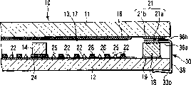
如图1至图4所示,FED包括由各矩形形状的玻璃板构成的正面基板11及背面基板12,对这些基板设置1~2mm的间隙,并相对配置。正面基板11及背面基板12通过矩形框状的侧壁18使其周边部相互结合,构成内部保持真空的扁平的矩形形状的真空外壳10。As shown in FIGS. 1 to 4 , the FED includes a front substrate 11 and a rear substrate 12 each composed of rectangular glass plates, and these substrates are arranged facing each other with a gap of 1 to 2 mm. The front substrate 11 and the rear substrate 12 are connected to each other at their peripheries by a rectangular frame-shaped side wall 18 to constitute a flat rectangular vacuum envelope 10 in which a vacuum is maintained.

在真空外壳10的内部,设置用于支撑施加在正面基板11及背面基板12上的大气压负荷的多个板状支持构件14。按与真空外壳10的一边平行的方向分别延伸,同时沿与上述一边正交的方向设置规定的间隔,来配置这些支持构件14。支持构件14不限于板状,也可使用柱状的形状。Inside the vacuum envelope 10 , a plurality of plate-shaped support members 14 are provided for supporting the atmospheric pressure load applied to the front substrate 11 and the rear substrate 12 . These support members 14 are arranged so as to extend in a direction parallel to one side of the vacuum envelope 10 and to provide predetermined intervals in a direction perpendicular to the above-mentioned side. The supporting member 14 is not limited to a plate shape, and a columnar shape may also be used.

在正面基板11的内表面,形成作为图像显示面功能的荧光体屏幕16。通过将红、绿、蓝荧光体层R、G、B及位于这些荧光体层间的光吸收层20排列,来构成此荧光体屏幕16。按与真空外壳10的上述一边平行的方向延伸,同时沿与这一边正交的方向设置规定的间隔,来配置荧光体层R、G、B。光吸收层20设置在荧光体层R、G、B的周围。在荧光体屏幕16上,例如按顺序蒸镀由铝构成的金属衬垫17、吸附膜13。On the inner surface of the front substrate 11, a phosphor screen 16 functioning as an image display surface is formed. The phosphor screen 16 is formed by arranging red, green, and blue phosphor layers R, G, and B and a light absorbing layer 20 between these phosphor layers. Phosphor layers R, G, and B are arranged to extend in a direction parallel to the above-mentioned one side of the vacuum envelope 10 and to provide predetermined intervals in a direction perpendicular to this side. The light absorbing layer 20 is provided around the phosphor layers R, G, and B. As shown in FIG. On the phosphor screen 16 , for example, a metal spacer 17 made of aluminum and an adsorption film 13 are vapor-deposited in this order.

如图3所示,在背面基板12的内表面上,设置作为激励荧光体屏幕16的荧光体层的电子发射源的分别发射电子束的多数电子发射元件22。这些电子发射元件22对应于每一像素排列为多列及多行。详细地叙述,在背面基板12的内表面上形成导电性阴极层24,在这些导电性阴极层上形成具有多个模槽25的二氧化硅膜26。在二氧化硅26上形成由钼和铌等构成的栅电极28。在背面基板12的内表面上,在各模槽25内设置由钼等构成的锥状电子发射元件22。As shown in FIG. 3 , on the inner surface of rear substrate 12 , a plurality of electron emission elements 22 that respectively emit electron beams as electron emission sources that excite the phosphor layers of phosphor screen 16 are provided. These electron emission elements 22 are arranged in a plurality of columns and rows corresponding to each pixel. To describe in detail, the conductive cathode layer 24 is formed on the inner surface of the rear substrate 12, and the silicon dioxide film 26 having a plurality of mold grooves 25 is formed on these conductive cathode layers. A gate electrode 28 made of molybdenum, niobium, or the like is formed on the silicon dioxide 26 . On the inner surface of the rear substrate 12, a cone-shaped electron emission element 22 made of molybdenum or the like is provided in each cavity 25. As shown in FIG.

在上述结构的FED中,视频信号输入到以单纯矩阵方式形成的电子发射元件22和栅电极28。以电子发射元件22为基准的情况,在亮度最高的状态时,施加+100V的栅电压。此外,在荧光体屏幕16中施加+10kV。由此,从电子发射元件22发出电子束。从电子发射元件22发出的电子束的大小,能够通过栅电极28的来进行调制,通过由此电子束激励荧光体屏幕16的荧光体层,使其发光来显示图像。In the FED of the above structure, video signals are input to the electron emission elements 22 and the gate electrodes 28 formed in a simple matrix. When the electron emission element 22 is used as a reference, a gate voltage of +100V is applied in the state with the highest brightness. Furthermore, +10 kV is applied in the phosphor screen 16 . Thus, electron beams are emitted from the electron emission elements 22 . The size of the electron beam emitted from the electron emission element 22 can be modulated by the grid electrode 28, and the electron beam excites the phosphor layer of the phosphor screen 16 to emit light to display an image.

为了在荧光体屏幕16中施加高电压,在正面基板11、背面基板12、侧壁18及支持构件14用的玻璃基板中使用高熔点的玻璃。如后所述,利用烧结玻璃等低熔点玻璃19来封装背面基板12和侧壁18间隔。利用作为具有导电性的低熔点粘结材料的含铟(In)的粘结层21来粘结正面基板11和侧壁18的间隔。In order to apply a high voltage to phosphor screen 16 , glass with a high melting point is used for the glass substrates for front substrate 11 , rear substrate 12 , side wall 18 , and support member 14 . As will be described later, the space between the rear substrate 12 and the side wall 18 is sealed with a low-melting glass 19 such as frit glass. The gap between the front substrate 11 and the side wall 18 is bonded by an adhesive layer 21 containing indium (In), which is a conductive low-melting point adhesive material.

FED包括多个,例如一对电极30,这些电极以与粘结层21电导通的状态安装在外壳10上。这些电极30作为对粘结层21通电用的电极构件来使用。The FED includes a plurality of, for example, a pair of electrodes 30 , and these electrodes are mounted on the housing 10 in a state of being electrically connected to the adhesive layer 21 . These electrodes 30 are used as electrode members for passing electricity to the adhesive layer 21 .

如图5所示,例如,对作为导电构件的0.2mm厚的铜板进行加工,并将各电极30形成为夹子状。即,电极30,其截面形成为近似U字形状进行弯曲,具有平坦的第一板部33a,与此第一板部设置有间隙、相对的第二板部33b,相对于第一及第二板部以近似直角延伸和同时连接第一及第二板部的端缘部的导通部38。第一板部33a具有分别导通到粘结层21的第一及第二接触部36a、36b。在第一及第二接触部36a、36b之间形成隙缝45,将第二接触部36b形成为爪状,使其能容易进行弹性变形。As shown in FIG. 5 , for example, a 0.2 mm-thick copper plate as a conductive member is processed, and each electrode 30 is formed into a clip shape. That is, the electrode 30 is formed into a substantially U-shaped cross-section and bends, and has a flat first plate portion 33a with a gap, and an opposite second plate portion 33b that is opposite to the first and second plate portions. The plate portions extend at approximately right angles and simultaneously connect the conduction portions 38 of the end edge portions of the first and second plate portions. The first plate portion 33a has first and second contact portions 36a, 36b respectively connected to the adhesive layer 21 . A slit 45 is formed between the first and second contact portions 36a, 36b, and the second contact portion 36b is formed into a claw shape so as to be easily elastically deformable.

如图1至图3所示,例如,各电极30以与背面基板12及侧壁18弹性结合的状态,安装在真空外壳10上。即,电极30在第一板部33a和第二板部33b之间,以弹性夹持正面基板12的端缘部及侧壁18的状态固定在真空外壳10上。并且,第一板部33a的第一及第二接触部36a、36b分别接触粘结层21,并与其进行电导通。此外,电极30的导通部38相对背面基板12的侧面及侧壁18,露出到真空外壳10的外侧。这些一对电极30,分别设置在真空外壳10的对角方向间隔开的两个角部,相对于粘结层21对称地配置。As shown in FIGS. 1 to 3 , for example, each electrode 30 is mounted on the vacuum envelope 10 in a state of being elastically coupled to the rear substrate 12 and the side wall 18 . That is, the electrode 30 is fixed to the vacuum envelope 10 in a state of elastically sandwiching the edge portion of the front substrate 12 and the side wall 18 between the first plate portion 33a and the second plate portion 33b. In addition, the first and second contact portions 36a, 36b of the first plate portion 33a are in contact with the adhesive layer 21 and are electrically connected thereto. In addition, the conductive portion 38 of the electrode 30 is exposed to the outside of the vacuum envelope 10 relative to the side surface of the rear substrate 12 and the side wall 18 . The pair of electrodes 30 are respectively provided at two corners of the vacuum envelope 10 spaced apart in the diagonal direction, and are arranged symmetrically with respect to the adhesive layer 21 .

接下来,详细说明具有上述结构的FED的制造方法。Next, a method of manufacturing the FED having the above-mentioned structure will be described in detail.

首先,在作为正面基板11的板玻璃上形成荧光体屏幕16。此情况下,制备与正面基板11相同尺寸的板玻璃,在此板玻璃上通过绘图仪形成荧光体条纹图形。安装曝光台,该曝光台装载有形成此荧光体条纹图形的板玻璃和正面基板用的板玻璃定位的设备。在此状态下,通过曝光、显影荧光体条纹图形,在作为正面基板11的玻璃板上生成荧光体屏幕。此后,重合在荧光体屏幕上16,形成金属衬垫17。First, phosphor screen 16 is formed on plate glass as front substrate 11 . In this case, a plate glass having the same size as that of the front substrate 11 was prepared, and a phosphor stripe pattern was formed on this plate glass by a plotter. An exposure table is installed, and the exposure table is equipped with a plate glass for forming the phosphor stripe pattern and a plate glass positioning device for the front substrate. In this state, by exposing and developing the phosphor stripe pattern, a phosphor screen is formed on the glass plate as the front substrate 11 . Thereafter, the metal spacer 17 is formed by superimposing on the phosphor screen 16 .

接下来,在背面基板12用板玻璃上形成电子发射元件22。这是,在板玻璃上形成矩阵状的导电性阴极层24,在此阴极层上例如利用热氧化法和CVD法或溅射法形成二氧化硅膜的绝缘膜。此后,在此绝缘膜上,例如利用溅射法和电子束蒸镀法形成钼和铌等的栅电极形成用的金属膜。接下来,在此金属膜上,通过平板印刷术对应于所形成相应的栅电极的形状,形成抗蚀剂图形。将抗蚀剂图形作为掩模,利用湿法腐蚀法或干法腐蚀法蚀刻金属膜,形成栅电极28。Next, the electron emission element 22 is formed on the plate glass for the rear substrate 12 . Here, a matrix-shaped conductive cathode layer 24 is formed on a plate glass, and an insulating film of a silicon dioxide film is formed on the cathode layer by, for example, thermal oxidation, CVD, or sputtering. Thereafter, on this insulating film, a metal film for forming a gate electrode such as molybdenum or niobium is formed by, for example, sputtering or electron beam deposition. Next, on this metal film, a resist pattern is formed by lithography corresponding to the shape of the corresponding gate electrode to be formed. Using the resist pattern as a mask, the metal film is etched by wet etching or dry etching to form gate electrode 28 .

此后,将抗蚀剂图形及栅电极28作为掩模,利用湿法腐蚀法或干法腐蚀法蚀刻绝缘膜,形成模槽25。并且,在去除抗蚀剂图形后,通过相对于背面基板12表面,从规定角度倾斜的方向进行电子束蒸镀,在栅电极28上形成例如由铝和镍构成的剥离层。此后,从相对于背面基板表面垂直方向,利用电子束蒸镀法蒸镀阴极形成用的材料例如钼。由此,在模槽25的内部形成电子发射元件22。接下来,利用剥除法(liftoff)将剥离层与在其上形成的金属膜一起去除。继续,在大气下,利用低熔点玻璃19将侧壁18及支持部14封装在背面基板12的内表面。Thereafter, using the resist pattern and the gate electrode 28 as a mask, the insulating film is etched by wet etching or dry etching to form the cavity 25 . Then, after removing the resist pattern, electron beam vapor deposition is performed in a direction inclined from a predetermined angle with respect to the surface of rear substrate 12 to form a peeling layer made of, for example, aluminum and nickel on gate electrode 28 . Thereafter, a material for forming a cathode, such as molybdenum, is evaporated by an electron beam evaporation method from a direction perpendicular to the surface of the rear substrate. Thus, the electron emission element 22 is formed inside the cavity 25 . Next, the peeling layer is removed together with the metal film formed thereon by a liftoff method. Next, under the atmosphere, the sidewall 18 and the support portion 14 are encapsulated on the inner surface of the rear substrate 12 by using the low-melting glass 19 .

此后,如图6A、6B所示,通过整个测壁18的粘结面,进一步按规定的宽度及厚度涂敷铟,形成粘结层21a。同样地,按规定的宽度及厚度在与正面基板11的侧壁相对的粘结面上以矩形框状涂敷铟,形成粘结层21b。相对于侧壁18及正面基板11的粘结面的粘结层21a、21b的填充,如上所述,通过在粘结面涂敷熔融的铟的方法,或在粘结面装载固体状态的铟的方法来进行。Thereafter, as shown in FIGS. 6A and 6B , indium is further coated with a predetermined width and thickness across the entire adhesive surface of the measuring wall 18 to form an adhesive layer 21 a. Similarly, indium is coated in a rectangular frame shape on the bonding surface facing the side wall of the front substrate 11 with a predetermined width and thickness to form the bonding layer 21b. Filling of the adhesive layers 21a and 21b on the adhesive surfaces of the side walls 18 and the front substrate 11 is performed by applying molten indium to the adhesive surfaces or loading indium in a solid state on the adhesive surfaces as described above. method to proceed.

接下来。如图7所示,在结合侧壁18的背面基板12上安装一对电极30。此时,在侧壁18上,通过使各电极30的第一接触部36a接触粘结层21a,从而对于粘结层电连接电极。再有,为了完全地确保第一接触部36a和粘结层的导电性,预先焊上粘结层21a和第一接触部36a的间隙也是有效的。电极30,在基板上需要一对+极和-极,优选从各电极到粘结层21a、21b的通电长度相等。因此,将一对电极30安装在背面基板12的对角方向相对的两个角部,在各电极的两侧,将位于电极间的粘结层21a、21b的长度设定为几乎相等。next. As shown in FIG. 7 , a pair of electrodes 30 are mounted on the rear substrate 12 combined with the side walls 18 . At this time, the electrodes are electrically connected to the adhesive layer by making the first contact portion 36 a of each electrode 30 contact the adhesive layer 21 a on the side wall 18 . In addition, in order to completely ensure the electrical conductivity of the first contact portion 36a and the adhesive layer, it is also effective to pre-solder the gap between the adhesive layer 21a and the first contact portion 36a. The electrodes 30 require a pair of + poles and - poles on the substrate, and it is preferable that the lengths of electricity from each electrode to the adhesive layers 21a and 21b are equal. Therefore, a pair of electrodes 30 are mounted on two diagonally opposing corners of rear substrate 12, and the lengths of adhesive layers 21a and 21b between the electrodes are set to be substantially equal on both sides of each electrode.

安装电极30后,将这些背面基板12、正面基板11按规定间隔隔离,并相对配置,在此状态下,装入真空处理装置内。在此,使用例如如图9所示的真空处理装置100。真空处理装置100包括排列设置的装料室101、烘焙、电子射线清洗室102、冷却室103、吸附膜蒸发室104、安装室105、冷却室106及卸料室107。在安装室105连接通电用直流电源120和控制此电源的计算机122。真空处理装置100的各室构成能作为真空处理的处理室,在FED的制造时,能将整室真空排气。这些各处理室由未图示的选通阀门等连接。After mounting the electrodes 30, the rear substrate 12 and the front substrate 11 are spaced apart at predetermined intervals, arranged to face each other, and placed in a vacuum processing apparatus in this state. Here, for example, a vacuum processing apparatus 100 as shown in FIG. 9 is used. The vacuum processing device 100 includes a charging chamber 101 , a baking and electron beam cleaning chamber 102 , a cooling chamber 103 , an adsorption film evaporation chamber 104 , an installation chamber 105 , a cooling chamber 106 and an unloading chamber 107 . A DC power supply 120 for conducting electricity and a computer 122 for controlling the power supply are connected to the installation room 105 . Each chamber of the vacuum processing apparatus 100 constitutes a processing chamber that can be used for vacuum processing, and the entire chamber can be evacuated to vacuum during FED manufacturing. These processing chambers are connected by unshown gate valves and the like.

将以规定间隔隔离配置的上述正面基板11及背面基板12,首先装入装料室101内,在使装料室101内成为真空气氛后,向烘焙、电子射线清洗室102传送。The above-mentioned front substrate 11 and back substrate 12 arranged at predetermined intervals are first loaded into the charging chamber 101 , and after making the charging chamber 101 into a vacuum atmosphere, they are transported to the baking and electron beam cleaning chamber 102 .

在烘焙、电子射线清洗室102中,将各构件加热到300℃的温度,使各基板及侧壁的表面吸附气体发射。同时,对正面基板11的荧光体屏幕面及背面基板12的电子发射元件面照射来自设置在烘焙、电子射线清洗室102的未图示的电子射线发生装置的电子射线。此时,通过利用安装在电子射线发生装置外部的偏转装置偏转扫描电子射线,分别对荧光体屏幕面及电子发射元件面的整面进行电子射线清洗。In the baking and electron beam cleaning chamber 102, each member is heated to a temperature of 300° C., and the surface of each substrate and side wall is adsorbed to emit gas. Simultaneously, the phosphor screen surface of the front substrate 11 and the electron emission element surface of the rear substrate 12 are irradiated with electron beams from an electron beam generator (not shown) installed in the baking and electron beam cleaning chamber 102 . At this time, by deflecting and scanning electron beams by a deflection device installed outside the electron beam generator, electron beam cleaning is performed on the entire surfaces of the phosphor screen surface and the electron emitting element surface, respectively.

并且,将进行此加热、电子射线清洗的正面基板11及背面基板12送到冷却室103,直到冷却到约120℃的温度后,向吸附膜蒸镀室104传送。在蒸镀室104中,在荧光体层的外侧蒸镀Ba膜作为吸附膜。Ba膜能够防止表面被氧和碳等污染,维持活性状态。Then, the front substrate 11 and the rear substrate 12 subjected to the heating and electron beam cleaning are sent to the cooling chamber 103 , cooled to a temperature of about 120° C., and then transferred to the adsorption film deposition chamber 104 . In the vapor deposition chamber 104, a Ba film was vapor-deposited on the outside of the phosphor layer as an adsorption film. The Ba film can prevent the surface from being polluted by oxygen, carbon, etc., and maintain an active state.

接下来,将正面基板11及背面基板12送到安装室105。在此安装室105中,如图8所示,将正面基板11及背面基板12仍维持在约120℃,并将它们向相互接近的方向移动,使各电极30的第二接触部36b接触正面基板11侧的粘结层21b。由此,将各电极30电连接粘结层21b。此时,第二接触部36b,通过触压,对于粘结层21b进行弹性地按压,能够确保稳定的导电性。Next, the front substrate 11 and the rear substrate 12 are sent to the mounting chamber 105 . In this installation chamber 105, as shown in FIG. 8 , the front substrate 11 and the back substrate 12 are still maintained at about 120° C., and they are moved toward each other so that the second contact portion 36 b of each electrode 30 contacts the front surface. Adhesive layer 21b on the substrate 11 side. Thereby, each electrode 30 is electrically connected to the adhesive layer 21b. At this time, the second contact portion 36b elastically presses the adhesive layer 21b by contact pressure, so that stable electrical conductivity can be ensured.

接下来,如图10所示,在一对电极30电连接电源120后,分别对侧壁18侧的粘结层21a及正面基板11侧的粘结层21b通电,加热粘结层,并使铟熔融。此时,通过使连接电源120的连接端子40与电极30的导通部38接触,就能够完全地使电源和电极、以及电极和粘结层21a、21b导通。Next, as shown in FIG. 10, after the pair of electrodes 30 are electrically connected to the power source 120, the adhesive layer 21a on the side wall 18 side and the adhesive layer 21b on the front substrate 11 side are respectively energized, the adhesive layer is heated, and the Indium melts. At this time, by bringing the connection terminal 40 connected to the power supply 120 into contact with the conduction portion 38 of the electrode 30, the power supply and the electrode, and the electrode and the adhesive layers 21a and 21b can be completely conducted.

铟熔融后,对正面基板11及背面基板12按它们相互接近的方向加压。由此,使粘结层21a、21b融合,形成粘结层21,利用此粘结层21粘结正面基板11的周边部和侧壁18。将由上述工序形成的真空外壳10在冷却室106冷却到常温,从卸料室107取出。由此,完成FED真空外壳。After the indium is melted, pressure is applied to the front substrate 11 and the rear substrate 12 so that they approach each other. As a result, the adhesive layers 21 a and 21 b are fused to form the adhesive layer 21 , and the peripheral portion of the front substrate 11 and the side wall 18 are bonded together by the adhesive layer 21 . The vacuum envelope 10 formed through the above steps is cooled to normal temperature in the cooling chamber 106 and taken out from the unloading chamber 107 . Thus, the FED vacuum envelope is completed.

再有,在完成真空外壳后,如果需要也可将电极30切除。Also, after the vacuum envelope is completed, the electrodes 30 can be cut off if necessary.

根据以上这样结构的FED及其制造方法,将用于向粘结层21通电的电极30预先安装在外壳上,并以与粘结层电连接的状态固定。为此,加热时,通过电极30,能够在粘结层21流有稳定的电流。因此,在进行封装时,能够使构成粘结层的导电性的低熔点粘结材料在预定的通电时间内稳定,并且使粘结材料完全熔融,其结果,在粘结层21上不产生裂纹等,能够迅速并完全地进行封装。According to the FED structured as above and its manufacturing method, the electrodes 30 for supplying electricity to the adhesive layer 21 are preliminarily attached to the case and fixed in a state of being electrically connected to the adhesive layer. Therefore, during heating, a stable current can flow through the adhesive layer 21 through the electrode 30 . Therefore, when encapsulating, the conductive low-melting-point adhesive material constituting the adhesive layer can be stabilized for a predetermined energization time, and the adhesive material can be completely melted, and as a result, cracks do not occur on the adhesive layer 21. etc., can quickly and completely package.

由于在真空气氛中,进行正面基板及背面基板的封装、结合,所以通过并用烘焙和电子射线清洗,就能够充分地发射表面吸附气体,能够获得优良吸附能力的吸附膜。此外,由于利用通电加热来封装、粘贴铟,所以不需要加热整个正面基板及背面基板,能够减少吸附膜的劣化、封装工序中基板破裂等不合格,同时能够实现封装时间的缩短。Since the sealing and bonding of the front substrate and the rear substrate are carried out in a vacuum atmosphere, by combining baking and electron beam cleaning, the surface adsorption gas can be sufficiently emitted, and an adsorption film with excellent adsorption capacity can be obtained. In addition, since the indium is packaged and bonded by energized heating, it is not necessary to heat the entire front and back substrates, and it is possible to reduce defects such as deterioration of the adsorption film and cracking of the substrate during the packaging process, and shorten the packaging time.

因此,能够获得优良的量产性,同时,能够低价地获得可获得稳定且良好图像的FED。Therefore, an FED capable of obtaining stable and good images can be obtained at low cost while being excellent in mass productivity.

接下来,说明此发明的第二实施形态的FED。在上述的实施形态中,虽然各电极形成包括与侧壁侧的粘结层导通的第一接触部、及与上述正面基板侧的粘结层导通的第二接触部的结构,但根据第二实施形态,如图11、图12A及图12B所示,电极30形成包括单一的接触部36a的结构。一对电极30分别安装在背面基板12的对角方向相对的一对角部,以弹性夹持侧壁18及背面基板12的状态安装到外壳上。此时,各接触部36a,与粘结层21a的上面相接触,与粘结层电连接。Next, an FED according to a second embodiment of this invention will be described. In the above-mentioned embodiment, although each electrode has a structure including a first contact portion conducting to the adhesive layer on the side wall side and a second contact portion conducting to the adhesive layer on the front substrate side, according to In the second embodiment, as shown in FIGS. 11, 12A, and 12B, the electrode 30 has a structure including a single contact portion 36a. The pair of electrodes 30 are attached to a pair of diagonally opposite corners of the back substrate 12 , respectively, and attached to the casing in a state of elastically sandwiching the side wall 18 and the back substrate 12 . At this time, each contact portion 36a is in contact with the upper surface of the adhesive layer 21a, and is electrically connected to the adhesive layer.

在封装工序中,通过将形成粘结层21b的正面基板11与背面基板12相对配置,各电极30的接触部36a接触到粘结层21a、21b的两方,并与其电连接。并且,通过这些电极30,同时对粘结层21a、21b通电,就能够加热熔融铟。In the packaging process, by arranging front substrate 11 and rear substrate 12 on which adhesive layer 21b is formed to face each other, contact portion 36a of each electrode 30 comes into contact with both adhesive layers 21a, 21b and is electrically connected thereto. In addition, through these electrodes 30, the adhesive layers 21a and 21b are simultaneously energized to heat and melt indium.

在第二实施形态中,另一结构与上述第一实施形态相同,对相同的部分付与相同的参考符号,省略其详细说明。并且,即使在第二实施形态中,能够获得与第一实施形态相同的作用效果。再有,在第一及第二实施形态中,各电极30也可构成为安装固定在正面基板侧。In the second embodiment, another structure is the same as that of the above-mentioned first embodiment, and the same reference numerals are assigned to the same parts, and detailed description thereof will be omitted. Furthermore, also in the second embodiment, the same effect as that of the first embodiment can be obtained. Furthermore, in the first and second embodiments, each electrode 30 may be configured to be mounted and fixed on the front substrate side.

根据图13、图14A及图14B所示的第三实施形态,FED包括用于对在侧壁18上形成的粘结层21a通电的一对第一电极30a,和用于对在正面基板11上形成的粘结层21b通电的一对第二电极30b。第一及第二电极30a、30b与上述电极30相同形成为夹子状。但是,各电极和接触部36就成为一体。According to the third embodiment shown in FIG. 13, FIG. 14A and FIG. 14B, the FED includes a pair of first electrodes 30a for conducting electricity to the adhesive layer 21a formed on the side wall 18, and a pair of first electrodes 30a for connecting the adhesive layer 21a formed on the front side substrate 11. A pair of second electrodes 30b for conducting electricity on the adhesive layer 21b formed on it. The first and second electrodes 30a and 30b are formed in a clip shape similarly to the above-mentioned electrode 30 . However, each electrode and the contact portion 36 are integrated.

一对第一电极30a分别安装在背面基板12的对角方向相对的一对角部,以弹性夹持侧壁18及背面基板12的状态被安装。此时,各第一电极30a,其接触部36接触粘结层21a,与粘结层电连接。一对第二电极30b分别安装在正面基板11的对角方向相对的一对角部,以弹性夹持正面基板11的状态被安装。此时,各第二电极30b,其接触部36接触粘结层21b,与粘结层电连接。优选第一电极30a及第二电极30b不彼此重叠,分开配置于四个角部。The pair of first electrodes 30 a are respectively attached to a pair of corners opposite to each other in the diagonal direction of the back substrate 12 , and are attached in a state of elastically sandwiching the side wall 18 and the back substrate 12 . At this time, each first electrode 30a has its contact portion 36 in contact with the adhesive layer 21a, and is electrically connected to the adhesive layer. The pair of second electrodes 30b are attached to a pair of corners opposite to each other in the diagonal direction of the front substrate 11 , and are attached in a state of elastically sandwiching the front substrate 11 . At this time, each second electrode 30b has its contact portion 36 in contact with the adhesive layer 21b to be electrically connected to the adhesive layer. Preferably, the first electrode 30a and the second electrode 30b do not overlap with each other, and are separately arranged at four corners.

在封装工序中,如图13及图14A所示,使连接电源120的一对连接端子40a分别接触第一电极30a的导通部38,使电源和第一电极、及第二电极和粘结层21b导通。在此状态下,分别对侧壁18侧的粘结层21a及正面基板11侧的粘结层21b通电,加热粘结层,使铟熔融。In the packaging process, as shown in FIG. 13 and FIG. 14A, a pair of connection terminals 40a connected to the power supply 120 are respectively contacted with the conduction portion 38 of the first electrode 30a, and the power supply and the first electrode, and the second electrode and the second electrode are bonded together. Layer 21b conducts. In this state, electricity is applied to the adhesive layer 21 a on the side wall 18 side and the adhesive layer 21 b on the front substrate 11 side to heat the adhesive layer to melt indium.

铟熔融后,如图14B所示,对正面基板11及背面基板12按相互接近的方向加压。由此,使粘结层21a、21b融合,形成粘结层21,通过此粘结层粘结正面基板11的周边部和侧壁18。After the indium is melted, as shown in FIG. 14B , pressure is applied to the front substrate 11 and the rear substrate 12 in directions to approach each other. As a result, the adhesive layers 21 a and 21 b are fused to form the adhesive layer 21 , and the peripheral portion of the front substrate 11 and the side wall 18 are bonded together by this adhesive layer.

在第三实施形态中,另一结构与上述第一实施形态相同,对相同的部分付与相同的参考符号,省略其详细说明。并且,即使在第三实施形态中,能够获得与第一实施形态相同的作用效果。并且,在第三实施形态,能够个别地控制对正面基板12侧的粘结层21a及正面基板11侧的粘结层21b通电的电流值,能够进行更适合地通电加热。In the third embodiment, another structure is the same as that of the above-mentioned first embodiment, and the same reference numerals are assigned to the same parts, and detailed description thereof will be omitted. In addition, also in the third embodiment, the same effect as that of the first embodiment can be obtained. In addition, in the third embodiment, the current values for energizing the adhesive layer 21a on the front substrate 12 side and the adhesive layer 21b on the front substrate 11 side can be individually controlled, and more suitable energization heating can be performed.

接下来,说明此发明的第四实施形态的FED。Next, an FED according to a fourth embodiment of this invention will be described.

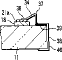
如图15至图17所示,FED包括真空外壳10及安装在真空外壳10的多个例如一对电极30。真空外壳10包括分别由矩形形状的玻璃板构成的正面基板11及背面基板12,这些基板11、12通过矩形框状侧壁18而使周边部相互结合。在正面基板11的内表面,形成有荧光体屏幕16、金属衬垫17、吸附膜13。在背面基板12的内表面上设置激励荧光体屏幕16的荧光体层的多个电子发射元件22。此外,在背面基板12的内表面,以矩阵状设置对电子发射元件22供给电位的多条布线23,将其端部引出到真空外壳10的周边部。As shown in FIGS. 15 to 17 , the FED includes a vacuum housing 10 and a plurality of, for example, a pair of electrodes 30 mounted on the vacuum housing 10 . The vacuum envelope 10 includes a front substrate 11 and a rear substrate 12 each formed of a rectangular glass plate, and peripheral portions of these substrates 11 and 12 are joined to each other by a rectangular frame-shaped side wall 18 . On the inner surface of the front substrate 11, a phosphor screen 16, a metal spacer 17, and an adsorption film 13 are formed. A plurality of electron emission elements 22 that excite the phosphor layer of the phosphor screen 16 are provided on the inner surface of the rear substrate 12 . In addition, on the inner surface of the rear substrate 12 , a plurality of wirings 23 for supplying potentials to the electron emission elements 22 are provided in a matrix, and the ends thereof are drawn out to the peripheral portion of the vacuum envelope 10 .

一对电极30以与粘结层21电导通的状态安装在外壳10。这些电极30作为向粘结层21通电时的电极来使用。例如将作为导电构件的0.2mm厚的铜板弯曲加工来形成各电极30。即,电极30,其截面形成为近似U字形状进行弯曲,整体包括夹持正面基板11或背面基板12的周边部,可安装的夹子状的安装部32、排列位于安装部的楔状壳体部34、位于壳体部的伸出端的接触部36、以及由安装部及壳体部的背部形成的平坦的导通部38。接触部36形成为在水平方向的延伸长度L为2mm以上。此外,壳体部34形成为带状,从接触部36向外侧的斜上方倾斜延伸。由此,壳体部34,沿垂直方向,形成位于高出接触部36的流出区分部37。The pair of electrodes 30 is attached to the case 10 in a state of being electrically connected to the adhesive layer 21 . These electrodes 30 are used as electrodes for passing electricity to the adhesive layer 21 . For example, each electrode 30 is formed by bending a 0.2 mm-thick copper plate as a conductive member. That is, the electrode 30 is formed into a substantially U-shaped cross-section to bend, and as a whole includes a clip-shaped mounting portion 32 that can be mounted by sandwiching the peripheral portion of the front substrate 11 or the rear substrate 12, and wedge-shaped housing portions arranged in the mounting portion. 34. The contact portion 36 located at the protruding end of the housing portion, and the flat conduction portion 38 formed by the mounting portion and the back of the housing portion. The contact portion 36 is formed such that the extension length L in the horizontal direction is 2 mm or more. Furthermore, the case portion 34 is formed in a belt shape and extends obliquely upward and outward from the contact portion 36 . Thus, the case part 34 forms an outflow partition part 37 located higher than the contact part 36 in the vertical direction.

各电极30,以弹性连接的状态安装在真空外壳10的例如背面基板12上。即,电极30利用安装部32以弹性夹持背面基板12的周边部的状态,安装在真空外壳10。各电极30的接触部36分别接触粘结层21,并与其电导通。壳体部34从接触部36延伸到真空外壳10的外侧,同时,流出区分部37沿垂直方向位于高出接触部36的位置。导通部38与背面基板12的侧面相对,露出到真空外壳10的外面。这些一对电极30,分别设置在真空外壳10的对角方向分离的两个角部,相对于粘结层21对称地配置。Each electrode 30 is mounted on, for example, the rear substrate 12 of the vacuum envelope 10 in a state of being elastically connected. That is, the electrode 30 is attached to the vacuum envelope 10 in a state where the peripheral portion of the rear substrate 12 is elastically sandwiched by the attaching portion 32 . The contact portions 36 of the electrodes 30 respectively contact the adhesive layer 21 and are electrically connected thereto. The case portion 34 extends from the contact portion 36 to the outside of the vacuum housing 10 , while the outflow partition portion 37 is positioned higher than the contact portion 36 in the vertical direction. Conductive portion 38 faces the side surface of rear substrate 12 and is exposed to the outside of vacuum envelope 10 . These pair of electrodes 30 are respectively provided at two corners separated in the diagonal direction of the vacuum envelope 10 , and arranged symmetrically with respect to the adhesive layer 21 .

上述FED的另一结构与上述第一实施形态相同,对相同的部分付与相同的参考符号,省略其详细说明。Another configuration of the above-mentioned FED is the same as that of the above-mentioned first embodiment, and the same reference numerals are assigned to the same parts, and detailed description thereof will be omitted.

接下来,详细说明上述FED的制造方法。此制造方法与上述第一实施形态的制造方法基本相同,重点说明不同的部分。Next, a method of manufacturing the above-mentioned FED will be described in detail. This manufacturing method is basically the same as the manufacturing method of the above-mentioned first embodiment, and the different parts will be explained emphatically.

首先,制备形成荧光体屏幕及金属衬垫17的正面基板11,以及形成电子发射元件22的背面基板12。接下来,在大气中,利用低熔点的玻璃19将侧壁18及支持构件14封装在背面基板12的内表面上。此后,如图18A、图18B所示,通过侧壁18的粘结面的四周以规定的宽度及厚度涂敷铟,形成粘结层21a。在与正面基板11的侧壁相对的粘结面上以规定的宽度及厚度将铟涂敷成矩形框状,形成粘结层21b。再有,相对于侧壁18及正面基板11的粘结面的粘结层21a、21b的填充,如上所述,利用对粘结面涂敷熔融的铟的方法或对粘结面装载固体状态的铟方法来进行。First, the front substrate 11 on which the phosphor screen and the metal spacer 17 are formed, and the rear substrate 12 on which the electron emission elements 22 are formed are prepared. Next, the side wall 18 and the support member 14 are sealed on the inner surface of the rear substrate 12 with the glass 19 having a low melting point in the atmosphere. Thereafter, as shown in FIGS. 18A and 18B , an adhesive layer 21 a is formed by coating indium with a predetermined width and thickness around the adhesive surface of the side wall 18 . On the bonding surface facing the side wall of the front substrate 11, indium is applied in a rectangular frame shape with a predetermined width and thickness to form the bonding layer 21b. In addition, for the filling of the adhesive layers 21a, 21b on the adhesive surfaces of the side walls 18 and the front substrate 11, as described above, the method of applying molten indium to the adhesive surfaces or loading a solid state on the adhesive surfaces is used. The indium method is carried out.

接下来,在结合侧壁18的背面基板12上安装一对电极30。此时,在侧壁18上,通过使各电极30的接触部36与粘结层21a接触,使电极对于粘结层电连接。一对电极30安装在背面基板12的对角方向的相对的两个角部,将位于电极间的粘结层21a、21b的长度在各电极的两侧设定为基本上相等。Next, a pair of electrodes 30 are mounted on the rear substrate 12 combined with the side walls 18 . At this time, the electrodes 30 are electrically connected to the adhesive layer by bringing the contact portion 36 of each electrode 30 into contact with the adhesive layer 21 a on the side wall 18 . A pair of electrodes 30 are mounted on opposite corners of the rear substrate 12 in the diagonal direction, and the lengths of the adhesive layers 21a and 21b between the electrodes are set to be substantially equal on both sides of the electrodes.

安装电极30后,将背面基板12、正面基板11隔开规定的间隔并相对配置,在此状态下,装入图9所示的真空处理装置内。正面基板11及背面基板12通过装料室101送到烘焙、电子射线清洗室102。在烘焙、电子射线清洗室102中,在300℃的温度下加热各种构件,发射各基板的表面吸附气体。同时,对正面基板11的荧光体屏幕面及背面基板12的电子发射元件面照射来自电子射线发生装置的电子射线,分别对荧光体屏幕面及电子发射元件面的整面进行电子射线清洗。After the electrode 30 is mounted, the rear substrate 12 and the front substrate 11 are arranged facing each other with a predetermined interval therebetween, and in this state, they are placed in a vacuum processing apparatus as shown in FIG. 9 . The front substrate 11 and the back substrate 12 are sent to the baking and electron beam cleaning chamber 102 through the charging chamber 101 . In the baking and electron beam cleaning chamber 102, various components are heated at a temperature of 300° C., and the surface-adsorbed gas of each substrate is emitted. Simultaneously, the phosphor screen surface of the front substrate 11 and the electron emission element surface of the back substrate 12 are irradiated with electron beams from the electron beam generator to clean the entire phosphor screen surface and the electron emission element surface respectively.

在烘焙工序中,加热粘结层21a、21b,使其熔融。背面基板12侧的粘结层21a,通过各电极30流出到外部。但是,在各电极30中由于设置位置高于接触部36的流出区分部37,所以通过此流出区分部,能够抑制熔融的铟流向背面基板的外侧。In the baking step, the adhesive layers 21a and 21b are heated and melted. The adhesive layer 21 a on the rear substrate 12 side flows out to the outside through the electrodes 30 . However, since each electrode 30 is provided at a position higher than the outflow section 37 of the contact portion 36, the outflow section can suppress molten indium from flowing to the outside of the rear substrate.

接下来,将正面基板11及背面基板12送入冷却室103,冷却到约120℃的温度后,送向吸附膜的蒸镀室104,在荧光体层的外侧蒸镀形成Ba膜。接下来,将正面基板11及背面基板12送入安装室105,如图19所示,在相对配置的状态下,分别保持在安装室内的热板131、132上。为了不使正面基板11落下,利用固定工具133将其固定在上侧的热板131上。Next, the front substrate 11 and the back substrate 12 are sent to the cooling chamber 103, cooled to a temperature of about 120°C, and then sent to the adsorption film deposition chamber 104, where a Ba film is deposited on the outside of the phosphor layer. Next, the front substrate 11 and the rear substrate 12 are brought into the installation chamber 105, and as shown in FIG. 19, they are respectively held on the hot plates 131 and 132 in the installation chamber in a state of facing each other. In order not to drop the front substrate 11 , it is fixed to the upper hot plate 131 with a fixing tool 133 .

此后,继续将正面基板11及背面基板12维持在约120℃,并使其向相互接近的方向移动,以规定的压力加压。由此,将各电极30的接触部36夹持在正面基板11侧的粘结层21b和背面基板12侧的粘结层21a之间,将各电极30电连接粘结层21a、21b。此时,由于将接触部36形成为2mm以上的水平方向长度,就能够稳定地与粘结层21a、21b接触。再有,由于在电极30的接触部36预先涂敷铟,就更稳定,能够对粘结材料通电。Thereafter, the front substrate 11 and the rear substrate 12 are continuously maintained at about 120° C., moved toward each other, and pressed at a predetermined pressure. Thus, the contact portion 36 of each electrode 30 is sandwiched between the adhesive layer 21b on the front substrate 11 side and the adhesive layer 21a on the rear substrate 12 side, and each electrode 30 is electrically connected to the adhesive layers 21a, 21b. At this time, since the contact portion 36 is formed to have a length in the horizontal direction of 2 mm or more, it can be stably contacted with the adhesive layers 21a, 21b. Furthermore, since indium is preliminarily applied to the contact portion 36 of the electrode 30, it is more stable, and electricity can be passed to the bonding material.

在此状态下,将电源120电连接一对电极30后,以恒流模式分别对侧壁18侧的粘结层21a及正面基板11侧的粘结层21b施加例如140A的直流电流。由此,加热粘结层21a、21b,使铟熔融。此时,通过使连接电源120的接续端子接触电极30的导通部38,就能够完全使电源和电极、及电极和粘结层21a、21b导通。此外,由于各电极30对于粘结层21a、21b等效地接触,所以能够使其稳定并通电,能够在各粘结层流过几乎等量的电流,并使其均等地熔融。In this state, after the power supply 120 is electrically connected to the pair of electrodes 30, a direct current of, for example, 140A is applied to the adhesive layer 21a on the sidewall 18 side and the adhesive layer 21b on the front substrate 11 side in a constant current mode. Thereby, the adhesive layers 21a and 21b are heated to melt indium. At this time, by bringing the connection terminal connected to the power supply 120 into contact with the conduction portion 38 of the electrode 30, the power supply and the electrode, and the electrode and the adhesive layers 21a and 21b can be completely conducted. In addition, since each electrode 30 is in equivalent contact with the adhesive layers 21a, 21b, it can be stably and electrically energized, and a substantially equal amount of current can flow through each adhesive layer to melt them equally.

如上所述,通过使铟熔融,使粘结层21a、21b熔融形成粘结层21,利用此粘结层粘结正面基板11的周边部及侧壁1 8。使由上述工序形成的真空外壳10,在冷却室106冷却到常温,从卸料室107取出。由此,完成真空外壳10。再有,在完成真空外壳10后,如需要也可以切除电极30。As described above, by melting indium, the adhesive layers 21a and 21b are melted to form the adhesive layer 21, and the peripheral portion of the front substrate 11 and the side wall 18 are bonded by this adhesive layer. The vacuum envelope 10 formed by the above steps is cooled to normal temperature in the cooling chamber 106 and taken out from the unloading chamber 107 . Thus, the vacuum envelope 10 is completed. In addition, after completion of the vacuum envelope 10, the electrodes 30 may be cut off if necessary.

根据上述结构的FED及其制造方法,能够获得与上述第一实施形态相同的作用效果。并且,根据第四实施形态,用于对粘结材料通电的电极30,由于具有位于高于接触部的流出区分部,所以在烘焙工序等中,将熔融的粘结材料区分出通过电极流出到外部的粘结材料。为此,将粘结层维持在均匀的厚度,能够通过四周完全封装外壳,同时,能够防止由粘结材料的流出引起的布线短路等。因此,能够获得优良的量产性,同时,能够低价地获得可获得稳定且良好图像的FED。According to the FED having the above-mentioned structure and its manufacturing method, the same effects as those of the above-mentioned first embodiment can be obtained. Furthermore, according to the fourth embodiment, since the electrode 30 for energizing the bonding material has an outflow region located higher than the contact portion, the molten bonding material is separated and flows out through the electrode in the baking process or the like. External bonding material. Therefore, by maintaining the adhesive layer at a uniform thickness, the case can be completely encapsulated around the periphery, and at the same time, it is possible to prevent wiring short-circuits and the like caused by the adhesive material flowing out. Therefore, an FED capable of obtaining stable and good images can be obtained at low cost while being excellent in mass productivity.

在上述第四实施形态中,虽然各电极30的壳体部34形成为其几乎整体从接触部36向斜上方延伸,形成流出区分部37的结构,也可以例如,如图20所示,将壳体部34的一部分,沿垂直方向,向高于接触部36的位置延伸,构成流出区分部37。此外,虽然各电极30作为整体具备安装部的结构,但如图21、图22所示,将电极30构成包括接触部36、壳体部34、流出区分部37及基台部39的结构,也可构成使用其它的夹具46在正面基板12上安装的结构。In the above-mentioned fourth embodiment, although the casing portion 34 of each electrode 30 is formed to extend obliquely upward from the contact portion 36 almost entirely to form the outflow partition portion 37, for example, as shown in FIG. A part of the case portion 34 extends vertically to a position higher than the contact portion 36 to form an outflow partition portion 37 . In addition, although each electrode 30 has a structure of a mounting part as a whole, as shown in FIGS. A structure in which other jigs 46 are used to mount on the front substrate 12 is also possible.

再有,在图20至图22所示的变化例中,另一结构与上述第四实施形态相同,对相同的部分付与相同的参考符号,并省略其详细说明。并且,即使在使用这些变化例的电极的情况下,也能够获得与上述实施形态相同的作用效果。In addition, in the modified examples shown in FIGS. 20 to 22 , another structure is the same as that of the above-mentioned fourth embodiment, and the same reference numerals are assigned to the same parts, and detailed description thereof will be omitted. Furthermore, even when the electrodes of these modified examples are used, the same effects as those of the above-described embodiment can be obtained.

其次,说明本发明第五实施形态的FED。Next, an FED according to a fifth embodiment of the present invention will be described.

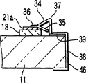
如图23至25所示,FED包括真空外壳10及安装在真空外壳上的多个,例如一对电极30。一对电极30以与粘结层21电导通的状态,安装在外壳10上。例如将作为导电构件的0.2mm厚的铜板弯曲加工来形成各电极30。即,将各电极30,其截面形成为近似U字形状进行弯曲,整体包括夹持正面基板11或背面基板12的周边部,可安装的夹子状的安装部32、排列位于安装部的楔状壳体部34、位于壳体部的伸出端的接触部36、从接触部向壳体部侧延伸,与壳体部并列位置的泄放部35、以及由安装部及壳体部的背面部形成的平坦的导通部38。As shown in FIGS. 23 to 25, the FED includes a vacuum envelope 10 and a plurality of, for example, a pair of electrodes 30 mounted on the vacuum envelope. A pair of electrodes 30 are attached to the case 10 in a state of being electrically connected to the adhesive layer 21 . For example, each electrode 30 is formed by bending a 0.2 mm-thick copper plate as a conductive member. That is, each electrode 30 is formed into a substantially U-shaped cross-section and bent, and the whole includes a clip-shaped mounting portion 32 that can be mounted by clamping the peripheral portion of the front substrate 11 or the rear substrate 12, and wedge-shaped shells arranged in the mounting portion. The body part 34, the contact part 36 located at the protruding end of the case part, the discharge part 35 extending from the contact part to the case part side, and the position parallel to the case part, and formed by the mounting part and the back part of the case part The flat conduction portion 38.

接触部36形成为在水平方向的延伸长度L为2mm以上。壳体部34形成为带状,从接触部36向外侧的斜上方倾斜延伸。由此,壳体部34,沿垂直方向,形成位于高出接触部36的位置上的流出区分部37。壳体部34形成从导通部38向接触部36流过电流的流路。The contact portion 36 is formed such that the extension length L in the horizontal direction is 2 mm or more. The case portion 34 is formed in a belt shape and extends obliquely upward and outward from the contact portion 36 . As a result, the case portion 34 forms an outflow partition portion 37 at a position higher than the contact portion 36 in the vertical direction. The case portion 34 forms a flow path through which current flows from the conduction portion 38 to the contact portion 36 .

泄放部35形成为带状,从接触部36向外侧的斜下方倾斜延伸。由此,沿垂直方向,在比接触部36低的位置形成泄放部35。泄放部35的宽度比壳体部34的宽度狭窄,例如形成为1mm左右。泄放部35,如后所述,形成使熔融的粘结材料流出到外部的流路。The relief portion 35 is formed in a belt shape and extends obliquely downward from the contact portion 36 outward. Thus, the relief portion 35 is formed at a position lower than the contact portion 36 in the vertical direction. The relief part 35 is formed narrower than the case part 34 in width, for example, about 1 mm. The drain portion 35 forms a flow path through which the molten adhesive material flows out to the outside, as will be described later.

各电极30,以弹性结合的状态安装在真空外壳10的例如背面基板12上。即,电极30通过安装部32以弹性夹持背面基板12的周边部的状态安装在真空外壳10。各电极30的接触部36分别接触粘结层21,与粘结层电导通。壳体部34从接触部36向真空外壳10的外侧延伸,同时,流出区分部37沿垂直方向位于高于接触部36的位置。泄放部35从接触部36向真空外壳10的外侧延伸,沿垂直方向位于低于接触部36的位置。导通部38与背面基板12的侧面相对,露出到真空外壳10的外面。这些一对电极30分别设置在真空外壳10的对角方向分离的两个角部,相对于粘结层21对称地配置。Each electrode 30 is mounted on, for example, the rear substrate 12 of the vacuum envelope 10 in a state of being elastically bonded. That is, the electrode 30 is mounted on the vacuum envelope 10 in a state of elastically sandwiching the peripheral portion of the rear substrate 12 by the mounting portion 32 . The contact portion 36 of each electrode 30 is in contact with the adhesive layer 21 respectively, and electrically conducts with the adhesive layer. The case portion 34 extends from the contact portion 36 to the outside of the vacuum housing 10 , while the outflow partition portion 37 is positioned higher than the contact portion 36 in the vertical direction. The discharge portion 35 extends from the contact portion 36 to the outside of the vacuum housing 10 and is located at a position lower than the contact portion 36 in the vertical direction. Conductive portion 38 faces the side surface of rear substrate 12 and is exposed to the outside of vacuum envelope 10 . These pair of electrodes 30 are respectively provided at two corners separated in the diagonal direction of the vacuum envelope 10 , and arranged symmetrically with respect to the adhesive layer 21 .

上述FED的另一结构,与上述第四实施形态相同,对相同的部分付与相同的参考符号,并省略其详细说明。此外,利用与第四实施形态的制造方法相同的制造方法制造第五实施形态的FED。Another configuration of the above-mentioned FED is the same as that of the above-mentioned fourth embodiment, and the same reference numerals are assigned to the same parts, and detailed description thereof will be omitted. In addition, the FED of the fifth embodiment is manufactured by the same manufacturing method as that of the fourth embodiment.

根据第五实施形态,在烘焙工序中,加热粘结层21a、21b使其熔融。并且,背面基板12侧的粘结层21a,通过电极30流出到外部。在各电极30中,由于设置位置高于接触部36的流出区分部37,利用此流出区分部,能够抑制熔融的铟向背面基板的外侧泄漏。此外,熔融的铟的一部分,虽然从电极30的泄放部35向背面基板12的外侧泄漏,但由于将泄放部的宽度形成得比壳体部34的宽度狭窄,所以流出量很少。例如,与流出区分部37及无泄放部的电极比较,能够将熔融的铟的流出量抑制到1/10左右。若为此程度的流出量,能够防止所谓的相对粘结层的厚度变薄,自封装部容易泄漏的问题,以及所谓的流出的铟接触基板上的布线,发生短路的问题。According to the fifth embodiment, in the baking step, the adhesive layers 21a and 21b are heated and melted. Furthermore, the adhesive layer 21 a on the rear substrate 12 side flows out to the outside through the electrode 30 . In each electrode 30 , since the outflow section 37 is provided at a position higher than that of the contact part 36 , leakage of molten indium to the outside of the rear substrate can be suppressed by the outflow section. Also, part of the molten indium leaks from the drain portion 35 of the electrode 30 to the outside of the rear substrate 12 , but since the drain portion is formed narrower than the case portion 34 , the outflow amount is small. For example, the outflow amount of molten indium can be suppressed to about 1/10 compared with the outflow section 37 and the electrode without the drain section. Such an amount of outflow can prevent the so-called problem that the thickness of the opposing adhesive layer becomes thin, which easily leaks from the sealing part, and the so-called problem that the outflowed indium contacts the wiring on the substrate and causes a short circuit.

此外,在封装工序中,使粘结层21a、21b融合,形成粘结层21,利用此粘结层粘结正面基板11的周边部和侧壁18。此时,由于对正面基板11及背面基板12向相互接近的方向加压,挤碎熔融的铟,生成剩余的铟。此剩余的铟向基板侧流出。这里,在各电极30上在比接触部3b低的位置设置泄放部35,使剩余的铟积极地从泄放部35从基板的外侧流出。即,以比壳体部34狭窄的宽度形成电极30的泄放部35,由于对铟加压,所以将剩余的铟沿所有电极的泄放部35冲向基板周边侧。各电极30安装在背面基板12的角部,泄放部35从布线23向外的位置延伸。为此,沿泄放部35,流出的铟不接触布线23,能够防止因流出的铟而导致的布线短路等。再有,通过在电极30的泄放部35及其附近区域预先涂敷铟,就更稳定,能够使粘结材料流出。In addition, in the sealing process, the adhesive layers 21 a and 21 b are fused to form the adhesive layer 21 , and the peripheral portion of the front substrate 11 and the side wall 18 are bonded together by this adhesive layer. At this time, since the front substrate 11 and the rear substrate 12 are pressed toward each other, the melted indium is crushed and excess indium is generated. The remaining indium flows out to the substrate side. Here, the drain portion 35 is provided on each electrode 30 at a position lower than the contact portion 3b, and excess indium is actively flowed out from the drain portion 35 from the outside of the substrate. That is, the drain portion 35 of the electrode 30 is formed narrower than the case portion 34, and since the indium is pressurized, the remaining indium rushes toward the substrate peripheral side along the drain portion 35 of all the electrodes. Each electrode 30 is mounted on a corner portion of the rear substrate 12 , and the drain portion 35 extends outward from the wiring 23 . Therefore, along the drain portion 35 , the outflowing indium does not contact the wiring 23 , and it is possible to prevent wiring short-circuits and the like due to the outflowing indium. Furthermore, by pre-coating indium on the drain portion 35 of the electrode 30 and its vicinity, it becomes more stable and the adhesive material can flow out.

另外,根据第五实施形态的FED及其制造方法,能够获得与上述第一实施形态相同的作用效果。In addition, according to the FED of the fifth embodiment and its manufacturing method, the same effects as those of the above-mentioned first embodiment can be obtained.

在第五实施形态中,各电极30的壳体部34虽然构成为其近似整体从接触部向斜上方延伸,形成流出区分部37的结构,但例如,如图26所示,也可沿垂直方向,使壳体部34的一部分向高出接触部36的位置延伸,构成流出区分部37。In the fifth embodiment, although the case part 34 of each electrode 30 is configured to extend obliquely upward from the contact part as a whole to form the outflow partition part 37, for example, as shown in FIG. Direction, a part of the housing portion 34 extends to a position higher than the contact portion 36 to form an outflow partition portion 37 .

此外,在第五实施形态中,虽然各电极30作为整体包括安装部的结构,但如图27及图28所示,电极30作为包括接触部36、壳体部34、流出区分部37、泄放部35及基台部39的结构,但也可作为使用具有导通部38的另一屏幕46,安装在背面基板12上的结构。In addition, in the fifth embodiment, although each electrode 30 has a structure including a mounting part as a whole, as shown in FIG. 27 and FIG. Although the structure of the mounting portion 35 and the base portion 39 is used, another screen 46 having the conduction portion 38 and mounted on the rear substrate 12 may also be used.

电极30的泄放部35不限于在壳体部34的侧面排列设置的结构,如图27所示,也可设置在壳体部34的中央部。此时,切割并翘起壳体部34的一部分来形成泄放部35,在壳体部形成允许粘结材料从接触部36向泄放部35流出的开口42。The discharge part 35 of the electrode 30 is not limited to the structure arranged side by side of the case part 34 , and may be provided in the center part of the case part 34 as shown in FIG. 27 . At this time, a part of the case part 34 is cut and raised to form the discharge part 35 , and an opening 42 for allowing the adhesive material to flow out from the contact part 36 to the discharge part 35 is formed in the case part.

此外,如图29所示,电极30的泄放部35未限于一个,也可在壳体部34的两侧设置一对。此时,各泄放部35的结构与上述实施形态相同。此外,In addition, as shown in FIG. 29 , the discharge portion 35 of the electrode 30 is not limited to one, and a pair may be provided on both sides of the case portion 34 . At this time, the structure of each relief part 35 is the same as that of the above-mentioned embodiment. also,

在图26至图29所示的变化例中,另一结构与上述第五实施形态相同,对相同的部分付与相同的参考符号,并省略其详细说明。并且,即使在使用这些变化例的情况下,也能够获得与上述实施形态相同的作用效果。此外,也可使用将上述实施形态及图26至图29所示的变化例相互组合的结构。In the modified examples shown in FIGS. 26 to 29 , another structure is the same as that of the above-mentioned fifth embodiment, and the same reference numerals are assigned to the same parts, and detailed description thereof will be omitted. Furthermore, even when these modified examples are used, the same effects as those of the above-described embodiment can be obtained. In addition, it is also possible to use a configuration in which the above-described embodiment and the modified examples shown in FIGS. 26 to 29 are combined.

接下来,说明本发明第六实施形态的FED及其制造方法。如图30所示,FED包括扁平的矩形形状的真空外壳10及在外壳安装的多个例如一对电极30。在第六实施形态中,由于FED的结构,除电极30以外,与上述的实施形态相同,所以重点说明不同的结构。同时,与制造方法一起说明FED的结构。Next, an FED according to a sixth embodiment of the present invention and its manufacturing method will be described. As shown in FIG. 30 , the FED includes a flat rectangular vacuum envelope 10 and a plurality of, for example, a pair of electrodes 30 attached to the envelope. In the sixth embodiment, since the structure of the FED is the same as that of the above-mentioned embodiment except for the electrode 30, the description will focus on the different structures. Meanwhile, the structure of the FED will be explained together with the manufacturing method.

如图13A及图13B所示,制备形成荧光体屏幕16及金属衬垫17的正面基板11,以及形成电子发射元件的背面基板12。接下来,在大气中,利用低熔点的玻璃将侧壁18及支持构件14封装在背面基板12的内表面上。此后,通过侧壁18的粘结面的四周以规定的宽度及厚度涂敷铟,形成矩形框状的粘结层21a。在与正面基板11的侧壁相对的粘结面上以规定的宽度及厚度将铟涂敷成矩形框状,形成对应于背面基板12侧的粘结层21a的矩形框状的粘结层21b。再有,相对于侧壁18及正面基板11的粘结面的粘结层21a、21b的填充,如上所述,利用对粘结面涂敷熔融的铟的方法或对粘结面装载固体状态的铟方法来进行。As shown in FIGS. 13A and 13B , a front substrate 11 on which phosphor screens 16 and metal spacers 17 are formed, and a rear substrate 12 on which electron-emitting elements are formed are prepared. Next, in the air, the side wall 18 and the support member 14 are sealed on the inner surface of the rear substrate 12 with glass having a low melting point. Thereafter, indium is applied around the adhesive surface of the side wall 18 with a predetermined width and thickness to form a rectangular frame-shaped adhesive layer 21a. Indium is coated in a rectangular frame shape with a predetermined width and thickness on the adhesive surface facing the side wall of the front substrate 11 to form a rectangular frame-shaped adhesive layer 21b corresponding to the adhesive layer 21a on the rear substrate 12 side. . In addition, for the filling of the adhesive layers 21a, 21b on the adhesive surfaces of the side walls 18 and the front substrate 11, as described above, the method of applying molten indium to the adhesive surfaces or loading a solid state on the adhesive surfaces is used. The indium method is carried out.

接下来,将正面基板11及背面基板12、送入例如图9所示的真空处理装置内,在真空气氛中,进行封装。此时,加热正面基板11及背面基板12充分排气。将加热温度适当地设定为200℃~500℃。通过此排气处理,减少了自外壳构成构件的内壁发射的气体,防止真空外壳的真空度劣化。接下来,在正面基板11的荧光体屏幕16上形成吸附膜。这是为了利用吸附膜对成为真空外壳后的残留气体进行吸附排气,良好地保证真空外壳内的真空度。Next, the front substrate 11 and the back substrate 12 are transported into, for example, a vacuum processing apparatus as shown in FIG. 9 , and packaged in a vacuum atmosphere. At this time, the heated front substrate 11 and the rear substrate 12 are sufficiently exhausted. The heating temperature is appropriately set to 200°C to 500°C. Through this evacuation process, the gas emitted from the inner wall of the housing constituent member is reduced, preventing the vacuum degree of the vacuum housing from deteriorating. Next, an adsorption film is formed on phosphor screen 16 of front substrate 11 . This is to use the adsorption film to absorb and exhaust the residual gas after becoming the vacuum envelope, so as to ensure a good degree of vacuum in the vacuum envelope.

接下来,将相对荧光体屏幕16和电子发射元件的正面基板11及背面基板12相互重合在规定的位置。在此状态下,对粘结层21a、21b通电,加热并熔化这些粘结材料。此后,停止通电,使粘结层21a、21b的热快速扩散传导到正面基板11及侧壁18,使粘结层21a、21b固化。其结果,利用粘结层21a、21b使正面基板11和侧壁18相互封装。Next, the front substrate 11 and the rear substrate 12 facing the phosphor screen 16 and the electron emission elements are superimposed on each other at predetermined positions. In this state, electricity is applied to the adhesive layers 21a, 21b to heat and melt these adhesive materials. Thereafter, the power supply is stopped, and the heat of the adhesive layers 21a, 21b is quickly diffused and conducted to the front substrate 11 and the side wall 18, so that the adhesive layers 21a, 21b are cured. As a result, the front substrate 11 and the side wall 18 are sealed together by the adhesive layers 21a and 21b.

接下来,进一步详细说明上述封装工序。Next, the above-mentioned encapsulation process will be described in more detail.

如图31、32所示,在封装前的状态下,将正面基板11及背面基板12的温度设定得比粘结层21a、21b的熔点低,将粘结层21a、21b固化。在此状态下,将正面基板11及背面基板12重合在规定位置,使粘结层21a、21b相互重合。并且,利用加压装置23a、23b对正面基板11及背面基板12按相互接近的方向施加规定的负重。图像显示区域通过支持构件14保持规定的间隙。As shown in FIGS. 31 and 32 , before packaging, the temperatures of front substrate 11 and rear substrate 12 are set lower than the melting points of adhesive layers 21a, 21b to cure adhesive layers 21a, 21b. In this state, the front substrate 11 and the rear substrate 12 are superimposed at predetermined positions so that the adhesive layers 21 a and 21 b are superimposed on each other. Then, a predetermined load is applied to the front substrate 11 and the rear substrate 12 in directions approaching each other by the pressurizing devices 23a and 23b. The image display area maintains a predetermined gap through the supporting member 14 .

此时,在侧壁18的对角方向的相对的两个角部,在各粘结层21a、21b间夹持并配置板状电极30。如图31B所示,电极30,具有分别与粘结层电接触的两个接触部36a、36b,并形成近似Y字形状。此外,各电极30的接触部36a、36b在粘结层21a、21b的角部的两侧接触这些粘结层。在两个接触部36a、36b间,形成用于使熔融的粘结材料流出的间隙30c。作为电极30的夹持方法,能够使用由与电极30同材质的夹子等固定的方法。再有,电极30由至少含有Cu、AL、Fe、Ni、Co、Be、Cr任何一种的单元素或合金形成。At this time, the plate-like electrodes 30 are arranged between the respective adhesive layers 21 a and 21 b at two opposite corners in the diagonal direction of the side wall 18 . As shown in FIG. 31B, the electrode 30 has two contact portions 36a, 36b which are respectively in electrical contact with the adhesive layer, and is formed in a substantially Y-shape. Furthermore, the contact portions 36a, 36b of the respective electrodes 30 contact the adhesive layers 21a, 21b on both sides of the corner portions of these adhesive layers. Between the two contact portions 36a, 36b, a gap 30c is formed for the molten adhesive material to flow out. As a method of clamping the electrode 30 , a method of fixing with a clip or the like of the same material as the electrode 30 can be used. In addition, the electrode 30 is formed of a single element or an alloy containing at least any one of Cu, Al, Fe, Ni, Co, Be, and Cr.

接下来,分别使供电端子24a、24b接触电极30。这些供电端子24a、24b连接电源120。在此状态下,通过供电端子24a、24b及电极30,对粘结层21a、21b通以规定的电流时,仅粘结层21a、21b发热熔融。此时,熔融的剩余的粘结材料,通过由各电极30的两个36a、36b和粘结层所包围的间隙30c,从侧壁18的角部流出到侧壁的外部。Next, the power supply terminals 24a, 24b are brought into contact with the electrodes 30, respectively. These power supply terminals 24a and 24b are connected to a power supply 120 . In this state, when a predetermined current is passed through the adhesive layers 21a, 21b through the power supply terminals 24a, 24b and the electrodes 30, only the adhesive layers 21a, 21b will heat and melt. At this time, the remaining molten adhesive material flows out from the corner of the side wall 18 to the outside of the side wall through the gap 30c surrounded by the two 36a, 36b of each electrode 30 and the adhesive layer.

此后,停止通电,移开供电端子24a、24b时,热容量小的粘结层21a、21b的热因温度坡度而向正面基板11及侧壁18放热。粘结层21a、21b与热容量大的正面基板11及侧壁18达成热平衡,使其快速冷却固化。由此,获得具有通过粘结层21a、21b相互粘结正面基板11和侧壁18,高真空维持其内部的真空外壳10的FED。再有,封装后,电极30以与粘结层21a、21b一起封装的状态,固定在真空外壳10上。Thereafter, when the energization is stopped and the power supply terminals 24a, 24b are removed, the heat of the adhesive layers 21a, 21b with small heat capacity is released to the front substrate 11 and the side wall 18 due to the temperature gradient. The adhesive layers 21a, 21b reach a thermal balance with the front substrate 11 and the side wall 18 with large heat capacity, so that they can be rapidly cooled and solidified. Thereby, the FED having the vacuum envelope 10 in which the front substrate 11 and the side wall 18 are bonded to each other via the adhesive layers 21a and 21b and the interior is maintained at a high vacuum is obtained. In addition, after packaging, the electrode 30 is fixed to the vacuum envelope 10 in a state of being packaged together with the adhesive layers 21a and 21b.

根据上述这样的结构的第六实施形态的FEE及其制造方法,以极短的时间、利用简单的制造装置能够真空封装真空外壳。即,通过使用具有导电性的粘结材料,能够不加热基板,仅选择地加热热容量小、体积小的粘结材料,能够抑制因基板的热膨胀而产生的位置精度的劣化等。According to the FEE of the sixth embodiment having the above-mentioned structure and its manufacturing method, the vacuum envelope can be vacuum-sealed in a very short time with a simple manufacturing device. That is, by using a conductive adhesive material, it is possible to selectively heat only an adhesive material with a small heat capacity and a small volume without heating the substrate, thereby suppressing deterioration of positional accuracy due to thermal expansion of the substrate.

由于,粘结层的热容量与基板的热容量比非常的小,与加热整个基板的现有的方法比较,能够大幅度地缩减加热、冷却所花费的时间,能够大幅度地提高量产性。并且,封装所必需的装置仅为单一供电端子和接触它们的机构,所以能够实现极其简单且适于超高真空的的清洗装置。Since the ratio of the heat capacity of the adhesive layer to the heat capacity of the substrate is very small, compared with the conventional method of heating the entire substrate, the time spent on heating and cooling can be greatly reduced, and mass productivity can be greatly improved. In addition, the devices necessary for packaging are only a single power supply terminal and a mechanism for contacting them, so an extremely simple cleaning device suitable for ultra-high vacuum can be realized.

用于向粘结层21a、21b通电的各电极30具有多个接触部36a、36b,在这些接触部间形成有间隙30c。为此,封装时,能够使剩余的熔融状态的粘结材料从接触部36a、36b间的规定间隙30c积极地流出到外部。因此,通过将电极30的接触部设置在适当的位置,就能够防止粘结材料溢出到基板的布线上等,不产生布线间的短路,能够迅速稳定地封装。Each electrode 30 for passing electricity to the adhesive layers 21a, 21b has a plurality of contact portions 36a, 36b, and a gap 30c is formed between these contact portions. Therefore, at the time of packaging, the remaining molten adhesive material can be actively flowed out from the predetermined gap 30c between the contact portions 36a, 36b. Therefore, by providing the contact portion of the electrode 30 at an appropriate position, it is possible to prevent the adhesive material from spilling over the wiring on the substrate, etc., and it is possible to package quickly and stably without causing a short circuit between the wiring.

电极30在接触部间可具有连通粘结材料的间隙,不限定于上述Y字型形状,例如,如图33所示,也可为近似U字形状。电极30也可具有3个以上连接粘结材料的接触部。例如,如图34A所示,也可将电极30形成为具有四个接触部36a、36b、36c、36d的纺纱机形状。此时,在相邻接触部间形成连通粘结材料的间隙30c。The electrode 30 may have a gap through which the adhesive material is connected between the contact parts, and is not limited to the above-mentioned Y-shape, for example, may have a substantially U-shape as shown in FIG. 33 . The electrode 30 may have three or more contact portions to which the adhesive material is connected. For example, as shown in FIG. 34A, the electrode 30 may be formed in the shape of a spinning machine having four contact portions 36a, 36b, 36c, and 36d. At this time, gaps 30c communicating the adhesive material are formed between adjacent contact portions.

此外,电极30的接触部不限定于接触夹持真空外壳的角部的两侧,如图34b所示,也可在外壳的角部的一侧接触粘结层21a、21b。由于电极30位于稍稍偏离角部的位置,所以粘结材料从外壳的角部30d流出。再有,图33、图34a及图34B分别示出的变化例中,另一结构与上述实施形态相同,对相同的部分付与相同的参考符号,并省略其详细说明。此外,即使在这些变化例中,也能够获得与第六实施形态相同的作用效果。In addition, the contact portion of the electrode 30 is not limited to contacting both sides of the corner portion sandwiching the vacuum housing, as shown in FIG. Since the electrodes 30 are positioned slightly off the corners, the bonding material flows out from the corners 30d of the housing. 33, FIG. 34a, and FIG. 34B respectively show another configuration that is the same as the above-mentioned embodiment, and the same reference numerals are assigned to the same parts, and detailed description thereof will be omitted. In addition, even in these modification examples, the same operational effect as that of the sixth embodiment can be obtained.

在上述第六实施形态中,电极30构成为直接与粘结层21a、21b接触的结构,也可根据图35所示的第七实施形态的制造方法,构成预先用导电性材料层31覆盖电极30,通过这些导电性材料层31,使电极接触粘结层的结构。In the above-mentioned sixth embodiment, the electrode 30 is configured as a structure directly in contact with the adhesive layers 21a, 21b, but it may also be configured to cover the electrode with a conductive material layer 31 in advance according to the manufacturing method of the seventh embodiment shown in FIG. 30 , through these conductive material layers 31 , the electrode contacts the structure of the bonding layer.

即,在封装工序中,在粘结层21a和粘结层21b之间分别插入一对板状电极30。在各电极30中,与粘结层21a、21b接触的面预先由导电性材料层31覆盖。在此,各电极30的两面由与粘结层21a、21b相同的导电性材料的In或含In的合金覆盖。例如,利用超声波施加的电烙铁,通过对电极表面涂敷导电性材料来形成导电性材料层31。由此,各电极30通过导电性材料层31接触粘结层21a、21b。电极30由至少包含Cu、Al、Fe、Ni、Co、Be、Cr的任何一种单元素或合金形成。That is, in the packaging process, a pair of plate electrodes 30 are respectively inserted between the adhesive layer 21a and the adhesive layer 21b. In each electrode 30 , the surfaces in contact with the adhesive layers 21 a and 21 b are covered with the conductive material layer 31 in advance. Here, both surfaces of each electrode 30 are covered with In or an alloy containing In, which is the same conductive material as the adhesive layers 21a and 21b. For example, the conductive material layer 31 is formed by applying a conductive material to the electrode surface using a soldering iron that applies ultrasonic waves. Accordingly, each electrode 30 is in contact with the adhesive layers 21 a and 21 b via the conductive material layer 31 . The electrode 30 is formed of any single element or alloy containing at least Cu, Al, Fe, Ni, Co, Be, and Cr.

接下来,分别使供电端子24a、24b接触电极30。这些供电端子24a、24b连接电源120。在此状态下,通过供电端子24a、24b及电极30,对粘结层21a、21b通以规定的电流时,仅粘结材料发热熔化。此后,停止通电,移开供电端子24a、24b时,热容量小的粘结层21a、21b的热因温度坡度而向正面基板11及侧壁18放热。由此,粘结层21a、21b与热容量大的正面基板11及侧壁18达成热平衡,使其快速冷却固化。由此,获得具有通过粘结层21a、21b相互粘结正面基板11和侧壁18,高真空维持其内部的真空外壳10的FED。再有,封装后,电极30以与粘结层21a、21b一起封装的状态,固定在真空外壳10。Next, the power supply terminals 24a, 24b are brought into contact with the electrodes 30, respectively. These power supply terminals 24a and 24b are connected to a power supply 120 . In this state, when a predetermined current is passed through the adhesive layers 21a, 21b through the power supply terminals 24a, 24b and the electrodes 30, only the adhesive material will generate heat and melt. Thereafter, when the energization is stopped and the power supply terminals 24a, 24b are removed, the heat of the adhesive layers 21a, 21b with small heat capacity is released to the front substrate 11 and the side wall 18 due to the temperature gradient. As a result, the adhesive layers 21a, 21b reach a thermal balance with the front substrate 11 and the side walls 18 with large heat capacity, so that they can be rapidly cooled and solidified. Thereby, the FED having the vacuum envelope 10 in which the front substrate 11 and the side wall 18 are bonded to each other via the adhesive layers 21a and 21b and the interior is maintained at a high vacuum is obtained. In addition, after sealing, the electrode 30 is fixed to the vacuum envelope 10 in a state of being packaged together with the adhesive layers 21a and 21b.

在上述第七实施形态中,另一结构与上述第六实施形态相同,对相同的部分付与相同的参考符号,并省略其详细说明。省略其详细说明。此外,即使在上述这样结构的第七实施形态中,也能够获得与第六实施形态相同的作用效果。此外,用于向粘结层21a、21b通电的各电极30,其与粘结层的接触面由导电性材料层31覆盖。为此,粘结层21a、21b的通电熔融时,提高电极30和粘结材料的润湿性,能够防止粘结材料和电极之间的接触电阻的增加。由此,防止接触部的异常发热,能够不用担心所谓的粘结层21a、21b的开路。其结果,能够以短时间、高合格率制造FED。In the above-mentioned seventh embodiment, another structure is the same as that of the above-mentioned sixth embodiment, and the same reference numerals are assigned to the same parts, and detailed description thereof will be omitted. A detailed description thereof is omitted. In addition, even in the seventh embodiment configured as described above, the same operational effects as those of the sixth embodiment can be obtained. In addition, each electrode 30 for passing electricity to the adhesive layers 21 a and 21 b has a contact surface with the adhesive layer covered with a conductive material layer 31 . For this reason, when the adhesive layers 21a and 21b are energized and melted, the wettability between the electrode 30 and the adhesive material is improved, and an increase in the contact resistance between the adhesive material and the electrode can be prevented. Thereby, abnormal heat generation at the contact portion is prevented, and there is no need to worry about the so-called open circuit of the adhesive layers 21a and 21b. As a result, FEDs can be manufactured in a short time with a high yield.

此外,通过用导电性材料层31覆盖电极30的表面,能够将封装时剩余的熔融状态的粘结材料从电极向外壳的外部积极地排出。In addition, by covering the surface of the electrode 30 with the conductive material layer 31 , it is possible to actively discharge the molten adhesive material remaining at the time of packaging from the electrode to the outside of the case.

在上述的第七实施形态中,虽然构成将电极30插入粘结层21a、21b间的结构,但也可构成以使电极仅接触一个粘结材料的状态进行通电的结构。即,如图36所示,将正面基板11及背面基板12以规定位置重合,使粘结层21a、21b相互重合接触。对正面基板11及背面基板12,利用加压装置23a、23b,以按使其相互接近的方向施加规定的封装负重。并且,以分别接触粘结材料21b的状态配置电极30。In the seventh embodiment described above, although the electrode 30 is inserted between the adhesive layers 21a and 21b, it may be configured to conduct electricity while the electrode is in contact with only one adhesive material. That is, as shown in FIG. 36 , the front substrate 11 and the rear substrate 12 are superimposed at predetermined positions so that the adhesive layers 21 a and 21 b are superimposed and in contact with each other. A predetermined package load is applied to the front substrate 11 and the rear substrate 12 in such a direction that the pressing devices 23 a and 23 b approach each other. Furthermore, the electrodes 30 are arranged in a state of being in contact with the adhesive material 21b, respectively.

电极的保持方法,可以像预先连接正面基板11的粘结层21a、21b一样,用与粘结层相同材质的夹子等固定电极的方法,或着,也可以是利用夹子等将电极固定保持在供电端子24a、24b,在将正面基板11和背面基板12按规定位置重合时,将电极插入的方法。The holding method of the electrodes can be the same as connecting the bonding layers 21a and 21b of the front substrate 11 in advance, using clips or the like of the same material as the bonding layers to fix the electrodes, or the electrodes can be fixed and held by clips or the like. The power supply terminals 24a and 24b are a method of inserting electrodes when the front substrate 11 and the rear substrate 12 are overlapped at predetermined positions.

此时,在各电极30中,预先用导电性材料层31覆盖与粘结层21b接触的表面。例如,利用超声波施加的电烙铁,通过对电极表面涂敷导电性材料来形成导电性材料层31。再有,由于能够使封装时剩余的粘结材料从电极30积极地溢出,所以即使在不与电极的粘结材料连接的面也可形成导电性材料层。At this time, in each electrode 30 , the surface in contact with the adhesive layer 21 b is covered with the conductive material layer 31 in advance. For example, the conductive material layer 31 is formed by applying a conductive material to the electrode surface using a soldering iron that applies ultrasonic waves. Furthermore, since the remaining adhesive material during packaging can be positively overflowed from the electrode 30, a conductive material layer can be formed even on the surface that is not connected to the adhesive material of the electrode.

另一结构与上述第七实施形态相同,对相同的部分付与相同的参考符号,并省略其详细说明。并且,即使在上述结构中,也能够获得与第七实施形态相同的作用效果。The other configuration is the same as that of the above-mentioned seventh embodiment, and the same reference numerals are assigned to the same parts, and detailed description thereof will be omitted. Furthermore, even in the above configuration, the same operation and effect as that of the seventh embodiment can be obtained.

就对粘结材料通电的电流形态而言,不只是直流电流,也可使用以商用频率变动的交流电流。此情况下,能够省略将由交流送信过来的商用电流变换为特定的直流的时间,能够将装置简略化。并且,也可使用以kHz水平的高频变动的交流电流。此情况下,由于利用集肤效果,增加了仅相对于高频的实际电阻值增大部分的焦耳热,以更小的电流值能够得到与上述相同的加热效果。As for the form of electric current that energizes the bonding material, not only direct current but also alternating current that fluctuates at a commercial frequency may be used. In this case, it is possible to omit the time for converting the commercial electric current sent from the alternating current into a specific direct current, and simplify the device. In addition, an alternating current fluctuating at a high frequency of the kHz level may also be used. In this case, since the skin effect is used, Joule heat is increased only in the portion where the actual resistance value increases with respect to high frequencies, and the same heating effect as above can be obtained with a smaller current value.

此外,就通电电力和时间而言,在上述实施形态中设为5~300秒。通电时间长(电力小)时,产生由基板周边的温度上升而导致的冷却速度的下降和由热膨胀而导致的危害,通电时间短(电力大)时,产生因导电性粘结材料的填充不均匀而引起的开路和因玻璃热应力而导致的破裂。为此,通电的电力及时间(也包含时间的电力变化),优选对每个对象物进行最佳的条件设定。In addition, the energization power and time are set to 5 to 300 seconds in the above-mentioned embodiment. When the energization time is long (low power), the cooling rate decreases due to the temperature rise around the substrate and damage caused by thermal expansion occurs, and when the energization time is short (large power), insufficient filling of the conductive adhesive material occurs. Open circuits due to uniformity and cracks due to thermal stress on the glass. For this reason, it is preferable to set the optimum conditions for each object in terms of the power and time of energization (including power changes over time).

并且,就封装时的基板温度和粘结材料的熔点的温度差而言,在上述实施形态中设为20℃~150℃。在温度存在差异大的情况下,虽然能缩短冷却时间,但玻璃热应力增加,所以优选对每个对象设定最佳条件。In addition, the temperature difference between the substrate temperature during packaging and the melting point of the adhesive material is set to 20° C. to 150° C. in the above-mentioned embodiment. When there is a large difference in temperature, the cooling time can be shortened, but the thermal stress of the glass increases, so it is preferable to set the optimum conditions for each object.

接下来,说明本发明的第八实施形态的FED的制造方法。再有,在第八实施形态中,除FED的结构及制造方法的封装工序以外的结构与上述第六实施形态相同,重点说明不同部分。Next, a method of manufacturing an FED according to an eighth embodiment of the present invention will be described. In addition, in the eighth embodiment, the structure other than the structure of the FED and the packaging process of the manufacturing method is the same as that of the above-mentioned sixth embodiment, and the difference will be mainly explained.

如图37所示,在封装工序中,送入真空处理装置的安装室的正面基板11及背面基板12,相对于仍相对配置的热板131、132,其外表面分别保持为密封的状态。即,背面基板12装载在热板132上,为了使正面基板11不落下,通过固定工具133固定在上侧的热板131上。As shown in FIG. 37 , in the packaging process, the outer surfaces of the front substrate 11 and the rear substrate 12 carried into the installation chamber of the vacuum processing apparatus are kept sealed with respect to the hot plates 131 and 132 still facing each other. That is, the rear substrate 12 is mounted on the hot plate 132 , and is fixed to the upper hot plate 131 by the fixing tool 133 so that the front substrate 11 does not fall.

接下来,如图38及图39所示,制备一对例如由铜构成的厚约0.2mm的平板状电极30,将这些电极30插入正面基板11和背面基板12之间。此时,将一对电极30设置在相对的位置,各电极的前端插入到正面基板11侧的粘结层21b和背面基板12的粘结层21a之间的位置。例如,一对电极30分别配置在基板内、对角方向相对的两个角部、两个短边或两个长边。Next, as shown in FIGS. 38 and 39 , a pair of planar electrodes 30 made of, for example, copper with a thickness of about 0.2 mm is prepared, and these electrodes 30 are inserted between the front substrate 11 and the rear substrate 12 . At this time, a pair of electrodes 30 are provided at opposing positions, and the tip of each electrode is inserted between the adhesive layer 21 b on the front substrate 11 side and the adhesive layer 21 a on the rear substrate 12 . For example, the pair of electrodes 30 are respectively disposed on two corners, two short sides or two long sides facing each other in a diagonal direction within the substrate.

接下来,使上侧的热板131及正面基板11下降,使设置在正面基板11的粘结层21b的几乎整体接触设置在背面基板侧的侧壁18的粘结层21a。同时,在此,将正面基板11及背面基板12的至少一个基板,向将两基板相互接近的方向以所希望的压力加压。此时,在上下的粘结层21a、21b之间插入各电极30。由此,各电极30同时电接触上下的铟21。Next, the upper hot plate 131 and the front substrate 11 are lowered so that almost the whole of the adhesive layer 21b provided on the front substrate 11 contacts the adhesive layer 21a provided on the side wall 18 on the rear substrate side. At the same time, here, at least one of the front substrate 11 and the rear substrate 12 is pressurized with a desired pressure in a direction in which the two substrates approach each other. At this time, each electrode 30 is inserted between the upper and lower adhesive layers 21a, 21b. Accordingly, each electrode 30 electrically contacts the upper and lower indium 21 at the same time.

在此状态下,从电源通过一对电极30,以恒流模式对两粘结层21a、21b通以140A的直流电流。由此,加热形成粘结层的铟使其熔融,利用粘结层21a、21b密封结合正面基板11及侧壁18。In this state, a direct current of 140 A was passed through the pair of electrodes 30 from the power source to both adhesive layers 21 a and 21 b in a constant current mode. Thereby, the indium forming the adhesive layer is heated and melted, and the front substrate 11 and the side wall 18 are hermetically bonded by the adhesive layers 21a and 21b.

此后,通过停止通电,固化熔融的铟,形成外壳10。将像这样形成的外壳在冷却室106中冷却到常温,从卸料室107中取出。通过以上的工序,完成真空外壳。Thereafter, by stopping the energization, the molten indium is solidified to form the case 10 . The case thus formed is cooled to normal temperature in the cooling chamber 106 and taken out from the unloading chamber 107 . Through the above steps, the vacuum envelope is completed.

根据第八实施形态,与上述的实施形态相同,由于在真空气氛中进行正面基板11及背面基板12的封装、结合,所以能够通过并用烘焙和电子射线清洗使表面吸附气体充分发射,能够获得吸附能力优良的吸附膜。此外,由于利用通电加热铟来进行封装、结合,不需要加热正面基板及背面基板整体,能够不发生吸附膜的劣化、封装工序中基板破裂等不合格。同时,能够实现封装时间的缩短,能够作为量产性优良的制造方法。According to the eighth embodiment, since the front substrate 11 and the rear substrate 12 are packaged and bonded in a vacuum atmosphere as in the above-mentioned embodiments, the surface adsorption gas can be sufficiently emitted by combining baking and electron beam cleaning, and adsorption can be obtained. Excellent adsorption film. In addition, since the packaging and bonding are carried out by heating indium with electricity, it is not necessary to heat the entire front substrate and rear substrate, so that deterioration of the adsorption film and failures such as substrate cracking during the packaging process can be avoided. At the same time, shortening of packaging time can be achieved, and it can be used as a manufacturing method excellent in mass productivity.

此外,将相对配置的正面基板11及背面基板12的至少一个基板向使正面基板及背面基板相互接近的方向加压,在将粘结层21a、21b的至少一部分夹持在正面基板及背面基板的周边部间的状态,对粘结层通电,进行加热熔融。由此,形成将熔融后的粘结层夹在正面基板11和侧壁18之间的状态。因此,即使因沿基板的周边的粘结层21a、21b的截面积偏移和重力等而在熔融的铟产生局部的凹凸,由于能够限制正面基板11及侧壁18间的空间,能够将过剩的要凝结的熔融的铟压回稀疏的部分。其结果,能够抑制粘结层中的凹凸的产生。因此,熔融后的粘结层的截面积通过正面基板11及侧壁18的全周是均一的,结合时,能够通过整体均匀加粘结层。据此,由于防止因粘结层局部加热引起的开路、基板的破裂发生,能够进行稳定的结合。并且,能够提供一种可低价地制造、可靠性高且能够获得良好图像的FED。In addition, at least one of the facing substrate 11 and rear substrate 12 is pressed in a direction in which the front substrate and the rear substrate approach each other, and at least part of the adhesive layers 21a and 21b are sandwiched between the front substrate and the rear substrate. In the state between the peripheral parts, the adhesive layer is energized and heated and melted. As a result, the melted adhesive layer is sandwiched between the front substrate 11 and the side wall 18 . Therefore, even if local unevenness occurs in the molten indium due to the deviation of the cross-sectional area of the adhesive layers 21a, 21b along the periphery of the substrate, gravity, etc., since the space between the front substrate 11 and the side wall 18 can be restricted, the excess The molten indium to be condensed is pressed back into the sparser portion. As a result, occurrence of irregularities in the adhesive layer can be suppressed. Therefore, the cross-sectional area of the melted adhesive layer is uniform over the entire circumference of the front substrate 11 and the side wall 18, and the adhesive layer can be uniformly applied throughout the entirety during bonding. According to this, stable bonding can be performed by preventing an open circuit and a crack of the substrate due to local heating of the adhesive layer. In addition, it is possible to provide an FED that can be manufactured at low cost, has high reliability, and can obtain a good image.

根据上述的制造方法,将各电极30同时电接触正面基板11侧的粘结层21b及侧壁侧的粘结层21a这两方,即,能够以等效接触两粘结层的状态进行通电。由此,能够在各粘结层流过基本上等量的电流。其结果,均等地加热熔融设置在正面基板11及背面基板12的粘结层,能够进行稳定地结合。According to the above-mentioned manufacturing method, each electrode 30 can be electrically connected to both the adhesive layer 21b on the side of the front substrate 11 and the adhesive layer 21a on the side wall side at the same time, that is, it can be energized in a state of equivalently contacting the two adhesive layers. . Accordingly, a substantially equal amount of electric current can flow through each adhesive layer. As a result, the adhesive layers provided on the front substrate 11 and the rear substrate 12 are uniformly heated and melted, and stable bonding can be performed.

接下来,说明本发明第九实施形态的FED的制造方法。Next, a method of manufacturing an FED according to a ninth embodiment of the present invention will be described.

在上述的第八实施形态中,构成将电极30夹在上下粘结层21a、21b间,同时电接触粘结层的结构。根据第九实施形态,在接触电极30的部分中,预先部分熔接粘结层21a、21b,使电极30接触此溶敷部。In the above-described eighth embodiment, the electrode 30 is sandwiched between the upper and lower adhesive layers 21a, 21b, and is in electrical contact with the adhesive layers. According to the ninth embodiment, in the portion contacting the electrode 30, the adhesive layers 21a, 21b are partially welded in advance, and the electrode 30 is brought into contact with the welded portion.

详细叙述,送到真空处理装置的安装室105的正面基板11及背面基板12,如图40所示,由多个支持脚128保持,按相互接近的方向加压。由此,设置在正面基板11的粘结层21b及设置在侧壁18的粘结层21a相互接触。再有,在电极30接触的部分,例如,设置在正面基板11的粘结层21b,具有比另一部分更向外侧延伸的延伸部21c。例如,延伸部21c分别设置在正面基板11相对的两个角部附近。More specifically, the front substrate 11 and the rear substrate 12 sent to the installation chamber 105 of the vacuum processing apparatus are held by a plurality of support legs 128 as shown in FIG. Thus, the adhesive layer 21b provided on the front substrate 11 and the adhesive layer 21a provided on the side wall 18 are in contact with each other. In addition, the portion where the electrode 30 is in contact with, for example, the adhesive layer 21b provided on the front substrate 11 has an extension portion 21c extending outward from the other portion. For example, the extensions 21 c are respectively provided near two opposite corners of the front substrate 11 .

接下来,在对应于延伸部21c的位置,例如,在背面基板12的角部下方相对配置感应加热线圈127。利用此感应加热线圈127对粘结层21a、21b进行局部高频加热,部分溶敷粘结层。由此,在对角方向相对的两个角部分别形成溶敷部21d。Next, the induction heating coil 127 is disposed opposite to each other at a position corresponding to the extension portion 21c, for example, below the corner portion of the rear substrate 12 . The adhesive layers 21a and 21b are locally heated with high frequency by the induction heating coil 127 to partially melt the adhesive layers. Thereby, the welded part 21d is formed in each of two corner parts which oppose in a diagonal direction.

此后,在正面基板11和背面基板2之间插入由铜构成的厚约0.2mm的电极30,使其与各溶敷部21d的延伸部21c接触。在此状态下,自电源通过一对电极30对粘结层21a、21b通电。由此,加热熔融铟,利用粘结层21a、21b将正面基板11及侧壁18密封结合。Thereafter, an electrode 30 made of copper with a thickness of about 0.2 mm is inserted between the front substrate 11 and the rear substrate 2 so as to be in contact with the extension portion 21c of each welded portion 21d. In this state, the adhesive layers 21a and 21b are energized from the power source through the pair of electrodes 30 . Thereby, the indium is heated and melted, and the front substrate 11 and the side wall 18 are hermetically bonded by the adhesive layers 21a and 21b.

此后,通过停止通电,固化熔融的铟,形成外壳10。将像这样形成的外壳在冷却室中冷却到常温,从卸料室中取出。通过以上的工序,完成真空外壳。Thereafter, by stopping the energization, the molten indium is solidified to form the case 10 . The crust thus formed is cooled to normal temperature in a cooling chamber, and taken out of the unloading chamber. Through the above steps, the vacuum envelope is completed.

再有,另一结构与上述的实施形态相同,对相同的部分付与相同的参考符号,并省略其详细说明。In addition, another configuration is the same as the above-mentioned embodiment, and the same reference numerals are assigned to the same parts, and detailed description thereof will be omitted.

根据上述这样的第九实施形态,对于接触电极30的位置,通过使相对的铟在通电前相互溶敷,能够在正面基板11侧的粘结层21b及侧壁18侧的粘结层21a分流并流过基本上等量的电流。由此,能够均等加热熔融两粘结层21a、21b。此外,由于在以将正面基板11及背面基板12相互接近的方向对两基板加压的状态下,对粘结层通电,所以与上述第八实施形态相同,能够抑制熔融后的粘结层的截面积变化,能够均等对整个粘结层进行加热升温。根据以上的情况,能够获得将正面基板11及背面基板12稳定结合,可靠性高的FED。According to the ninth embodiment as described above, for the position of the contact electrode 30, by welding the opposing indiums to each other before energization, it is possible to shunt the flow between the adhesive layer 21b on the front substrate 11 side and the adhesive layer 21a on the side wall 18 side. and flow a substantially equal amount of current. Thereby, both adhesive layers 21a, 21b can be heat-melted equally. In addition, since the adhesive layer is energized in a state where the front substrate 11 and the rear substrate 12 are pressed in a direction to bring them closer to each other, the adhesive layer after melting can be suppressed similarly to the above-mentioned eighth embodiment. The change in cross-sectional area can evenly heat up the entire bonding layer. From the above, it is possible to obtain a highly reliable FED in which the front substrate 11 and the rear substrate 12 are stably bonded.

在第八及第九实施形态中,例如,也可在将电极预先安装在基板的状态下将其装入真空处理装置,电极的形状和材料也不仅限于上述实施形态的情况。此外,虽然构成以在正面基板及侧壁这两方设置粘结材料的状态进行封装的结构,但也可以以在正面基板及侧壁至少一个基板设置粘结材料的状态进行封装。In the eighth and ninth embodiments, for example, electrodes may be installed in a vacuum processing apparatus in a state where the electrodes are mounted on the substrate in advance, and the shape and material of the electrodes are not limited to those of the above-mentioned embodiments. In addition, although it is configured to package with an adhesive material provided on both the front substrate and the side wall, it may be packaged with an adhesive material provided on at least one of the front substrate and the side wall.

接下来,说明本发明的第十实施形态的FED及其制造方法。Next, an FED according to a tenth embodiment of the present invention and its manufacturing method will be described.

如图42及图43所示,FED包括真空外壳10及在真空外壳安装的多个例如一对电极30。真空外壳10包括分别由矩形形状的玻璃板构成的正面基板11及背面基板12,这些基板11、12通过矩形框状侧壁18与周边部相互结合。在正面基板11的内表面,形成有荧光体屏幕16、金属衬垫17、吸附膜13。在背面基板12的内表面上设置激励荧光体屏幕16的荧光体层的多个电子发射元件22。此外,在背面基板12的内表面中,以矩阵状设置对电子发射元件22供给电位的多条布线23,将其端部引出到真空外壳10的周边部。As shown in FIGS. 42 and 43 , the FED includes a vacuum envelope 10 and a plurality of, for example, a pair of electrodes 30 attached to the vacuum envelope. The vacuum envelope 10 includes a front substrate 11 and a rear substrate 12 each formed of a rectangular glass plate, and these substrates 11 , 12 are bonded to each other by a rectangular frame-shaped side wall 18 and a peripheral portion. On the inner surface of the front substrate 11, a phosphor screen 16, a metal spacer 17, and an adsorption film 13 are formed. A plurality of electron emission elements 22 that excite the phosphor layer of the phosphor screen 16 are provided on the inner surface of the rear substrate 12 . In addition, on the inner surface of the rear substrate 12 , a plurality of wirings 23 for supplying potentials to the electron emission elements 22 are provided in a matrix, and the ends thereof are drawn out to the peripheral portion of the vacuum envelope 10 .

一对电极30以与粘结层21电导通的状态安装在外壳10。这些电极30作为向粘结层21通电时的电极来使用。如图44所示,例如,将作为导电构件的0.2mm厚的铜板进行弯曲加工,以形成各电极30。即,将电极30的截面形成为近似U字形状来进行弯曲,整体包括安装部32、从安装部延伸出,对于粘结层成为电流通路的壳体部34、位于壳体部的伸出端,能接触粘结层的接触部36、以及由安装部及壳体部的背面部形成的平坦的导通部38。The pair of electrodes 30 is attached to the case 10 in a state of being electrically connected to the adhesive layer 21 . These electrodes 30 are used as electrodes for passing electricity to the adhesive layer 21 . As shown in FIG. 44 , for example, a 0.2 mm-thick copper plate as a conductive member is bent to form each electrode 30 . That is, the cross-section of the electrode 30 is formed into a substantially U-shape and bent, and the whole includes the mounting part 32, extending from the mounting part, and the case part 34, which becomes a current path for the adhesive layer, is located at the protruding end of the case part. , the contact portion 36 capable of contacting the adhesive layer, and the flat conduction portion 38 formed by the mounting portion and the back portion of the housing portion.

安装部32整体包括弯曲为夹子状的夹持部,能夹持正面基板11或背面基板12的周边部,进行安装。接触部36形成为在水平方向的延伸长度L为2mm以上。此外,壳体部34形成为带状,从安装部32向斜上方倾斜延伸。由此,接触部36,沿垂直方向,位于高出安装部32及壳体部34接触部36的位置。The mounting portion 32 generally includes a clamping portion bent into a clip shape, capable of clamping the peripheral portion of the front substrate 11 or the rear substrate 12 for mounting. The contact portion 36 is formed such that the extension length L in the horizontal direction is 2 mm or more. Furthermore, the case portion 34 is formed in a belt shape and extends obliquely upward from the mounting portion 32 . Thus, the contact portion 36 is located at a position higher than the contact portion 36 of the installation portion 32 and the housing portion 34 along the vertical direction.

如图42及图43、44所示,各电极30,通过真空外壳10的例如安装部32,以弹性夹持例如背面基板12的周边部的状态安装在真空外壳10。各电极30的接触部36分别接触粘结层21,并与其电导通。壳体部34从接触部36延伸到真空外壳10的外侧,同时,导通部38与背面基板12的侧面相对,露出到真空外壳10的外面。这些一对电极30,分别设置在真空外壳10的对角方向分离的两个角部,相对于粘结层21对称地配置。As shown in FIG. 42 and FIGS. 43 and 44 , each electrode 30 is attached to the vacuum housing 10 in a state of elastically sandwiching, for example, the peripheral portion of the rear substrate 12 via, for example, the mounting portion 32 of the vacuum housing 10 . The contact portions 36 of the electrodes 30 respectively contact the adhesive layer 21 and are electrically connected thereto. The case portion 34 extends from the contact portion 36 to the outside of the vacuum envelope 10 , while the conduction portion 38 faces the side surface of the rear substrate 12 and is exposed to the outside of the vacuum envelope 10 . These pair of electrodes 30 are respectively provided at two corners separated in the diagonal direction of the vacuum envelope 10 , and arranged symmetrically with respect to the adhesive layer 21 .

上述FED的另一结构与上述第一实施形态相同,对相同的部分付与相同的参考符号,省略其详细说明。Another configuration of the above-mentioned FED is the same as that of the above-mentioned first embodiment, and the same reference numerals are assigned to the same parts, and detailed description thereof will be omitted.

接下来,详细说明第十实施形态的FED的制造方法。在此,重点说明与上述第一实施形态的制造方法不同的部分。Next, the method of manufacturing the FED of the tenth embodiment will be described in detail. Here, the description will focus on differences from the manufacturing method of the first embodiment described above.

首先,与第一实施形态相同,制备形成荧光体屏幕16及金属衬垫17的正面基板11,以及形成电子发射元件22的背面基板12。接下来,在大气中,利用低熔点的玻璃19将侧壁18及支持构件14封装在背面基板12的内表面上。此后,通过侧壁18的粘结面的四周以规定的宽度及厚度涂敷铟,形成粘结层21a。在与正面基板11的侧壁相对的粘结面上以规定的宽度及厚度将铟涂敷成矩形框状,形成粘结层21b。First, as in the first embodiment, front substrate 11 on which phosphor screen 16 and metal spacer 17 are formed, and rear substrate 12 on which electron emission elements 22 are formed are prepared. Next, the side wall 18 and the support member 14 are sealed on the inner surface of the rear substrate 12 with the glass 19 having a low melting point in the atmosphere. Thereafter, indium is applied around the adhesive surface of the side wall 18 with a predetermined width and thickness to form an adhesive layer 21a. On the bonding surface facing the side wall of the front substrate 11, indium is applied in a rectangular frame shape with a predetermined width and thickness to form the bonding layer 21b.

接下来,如图45所示,在结合侧壁18的背面基板12上安装一对电极30。此时,接触部36与粘结层21a不接触,与粘结层设置间隙,以相对的状态安装各电极30。电极30,在基板上需要一对+极和-极,在一对电极间并列通电的粘结层21a、21b的各通电路径,优选其长度相等。因此,一对电极30安装在背面基板12的对角方向的相对的两个角部,将位于电极间的粘结层21a、21b的长度在各电极的两侧设定为基本上相等。Next, as shown in FIG. 45 , a pair of electrodes 30 are mounted on the rear substrate 12 bonded to the side walls 18 . At this time, the contact portion 36 is not in contact with the adhesive layer 21a, and a gap is provided with the adhesive layer, and each electrode 30 is attached in a facing state. The electrodes 30 require a pair of + poles and - poles on the substrate, and the current conduction paths of the adhesive layers 21a and 21b that conduct electricity in parallel between the pair of electrodes preferably have the same length. Therefore, a pair of electrodes 30 are mounted on opposite corners of the rear substrate 12 in the diagonal direction, and the lengths of the adhesive layers 21a and 21b between the electrodes are set to be substantially equal on both sides of the electrodes.

安装电极30后,将背面基板12、正面基板11隔开规定的间隔并相对配置,在此状态下,装入图9所示的真空处理装置100内。正面基板11及背面基板12通过装料室101送到烘焙、电子射线清洗室102。在烘焙、电子射线清洗室102中,在300℃的温度下加热各种构件,发射各基板的表面吸附气体。同时,对正面基板11的荧光体屏幕面及背面基板12的电子发射元件面照射来自电子射线发生装置的电子射线,分别对荧光体屏幕面及电子发射元件面的整面进行电子射线清洗。After the electrode 30 is mounted, the rear substrate 12 and the front substrate 11 are arranged facing each other with a predetermined interval therebetween, and in this state, they are loaded into the vacuum processing apparatus 100 shown in FIG. 9 . The front substrate 11 and the back substrate 12 are sent to the baking and electron beam cleaning chamber 102 through the charging chamber 101 . In the baking and electron beam cleaning chamber 102, various components are heated at a temperature of 300° C., and the surface-adsorbed gas of each substrate is emitted. Simultaneously, the phosphor screen surface of the front substrate 11 and the electron emission element surface of the back substrate 12 are irradiated with electron beams from the electron beam generator to clean the entire phosphor screen surface and the electron emission element surface respectively.

在烘焙工序中,通过加热,一旦熔融粘结层21a、21b,具有流动性,各电极30的接触部36不接触粘结层21a,21b,设置间隙并相对。为此,能够抑制熔融的铟通过电极30向背面基板12的外侧流出。In the baking process, once the adhesive layers 21a, 21b are melted by heating, they become fluid, and the contact portions 36 of the electrodes 30 do not contact the adhesive layers 21a, 21b, and face each other with a gap. For this reason, molten indium can be suppressed from flowing out to the outside of rear substrate 12 through electrode 30 .

将烘焙及电子射线清洗后的正面基板11及背面基板12送入冷却室103,冷却到约120℃的温度后,送向吸附膜的蒸镀室104。在此蒸镀室104中,在金属衬垫17的外侧蒸镀形成Ba膜作为吸附膜27。Ba膜能够防止氧和碳等污染表面,能够维持活性状态。The front substrate 11 and the rear substrate 12 after baking and electron beam cleaning are sent to the cooling chamber 103, and after being cooled to a temperature of about 120° C., they are sent to the evaporation chamber 104 for absorbing the film. In this vapor deposition chamber 104 , a Ba film is vapor-deposited on the outside of the metal pad 17 as the adsorption film 27 . The Ba film can prevent contamination of the surface with oxygen, carbon, etc., and can maintain an active state.

接下来,将正面基板11及背面基板12送入安装室105。如图46所示,在此安装室105中,将正面基板11及背面基板12在相对配置的状态下,分别保持在安装室内的热板131、132上。为了不使正面基板11落下,利用固定工具133将其固定在上侧的热板131上。Next, the front substrate 11 and the rear substrate 12 are carried into the mounting chamber 105 . As shown in FIG. 46 , in this mounting chamber 105 , the front substrate 11 and the rear substrate 12 are held on hot plates 131 , 132 in the mounting chamber in a state of facing each other. In order not to drop the front substrate 11 , it is fixed to the upper hot plate 131 with a fixing tool 133 .

此后,继续将正面基板11及背面基板12维持在约120℃,并使其向相互接近的方向移动,以规定的压力加压。基板的移动,可以是使正面基板11及背面基板12双方移动相互接近的方法,或也可是使正面基板及背面基板中的任何一个移动,并相互接近的方法。Thereafter, the front substrate 11 and the rear substrate 12 are continuously maintained at about 120° C., moved toward each other, and pressed at a predetermined pressure. The movement of the substrate may be a method of moving both the front substrate 11 and the rear substrate 12 close to each other, or a method of moving either one of the front substrate and the rear substrate so as to approach each other.

如图47所示,通过以规定的压力加压,使正面基板11侧的粘结层21b和背面基板12侧的粘结层21a相互接触,同时,将各电极30的接触部36夹持在粘结层21a、21b之间,将各电极30电连接粘结层21a、21b。此时,由于将接触部36形成为2mm以上的水平方向长度,就能够稳定地与粘结层21a、21b接触。再有,由于在电极30的接触部36预先涂敷铟,对于粘结层,就能够获得更良好接触及通电状态。As shown in FIG. 47, by pressing with a predetermined pressure, the adhesive layer 21b on the side of the front substrate 11 and the adhesive layer 21a on the side of the rear substrate 12 are brought into contact with each other, and at the same time, the contact portion 36 of each electrode 30 is sandwiched between them. Between the adhesive layers 21a, 21b, each electrode 30 is electrically connected to the adhesive layers 21a, 21b. At this time, since the contact portion 36 is formed to have a length in the horizontal direction of 2 mm or more, it can be stably contacted with the adhesive layers 21a, 21b. Furthermore, since indium is pre-coated on the contact portion 36 of the electrode 30, a better contact and conduction state can be obtained for the adhesive layer.

在此状态下,如图10所示,将电源120电连接一对电极30后,以恒流模式分别对侧壁18侧的粘结层21a及正面基板11侧的粘结层21b施加例如140A的直流电流。由此,加热粘结层21a、21b,使铟熔融。此时,通过使连接电源120的接续端子40接触电极30的导通部38,就能够完全使电源和电极、及电极和粘结层21a、21b导通。此外,由于各电极30对于粘结层21a、21b等效地接触,所以能够使其稳定并通电,能够在各粘结层流过几乎等量的电流,进行均等地加热熔融。In this state, as shown in FIG. 10 , after the power supply 120 is electrically connected to the pair of electrodes 30, apply, for example, 140A to the adhesive layer 21a on the side wall 18 side and the adhesive layer 21b on the side of the front substrate 11 in a constant current mode. of direct current. Thereby, the adhesive layers 21a and 21b are heated to melt indium. At this time, by bringing the connection terminal 40 connected to the power source 120 into contact with the conduction portion 38 of the electrode 30, the power source and the electrode, and the electrode and the adhesive layers 21a and 21b can be completely conducted. In addition, since each electrode 30 is in equivalent contact with the adhesive layers 21a and 21b, it can be stably and electrically energized, and a substantially equal amount of current can flow through each adhesive layer to perform uniform heating and melting.

通过使铟熔融,使粘结层21a、21b熔融形成粘结层21,利用此粘结层粘结正面基板11的周边部及侧壁18。将由上述工序封装的正面基板11、侧壁18、及背面基板12,在冷却室106冷却到常温,从卸料室107取出。由此,完成真空外壳10。By melting indium, the adhesive layers 21 a and 21 b are melted to form the adhesive layer 21 , and the peripheral portion of the front substrate 11 and the side wall 18 are bonded by this adhesive layer. The front substrate 11 , side wall 18 , and rear substrate 12 packaged in the above steps are cooled to normal temperature in the cooling chamber 106 and taken out from the unloading chamber 107 . Thus, the vacuum envelope 10 is completed.

再有,在完成真空外壳10后,如需要也可以切除一对电极30。In addition, after the vacuum envelope 10 is completed, the pair of electrodes 30 may be cut off if necessary.

根据以上这样结构的FED及其制造方法,通电加热时,通过安装在背面基板的电极30,能够在粘结层21流过稳定的电流。因此,在进行封装时,能够使构成粘结层的导电性的低熔点粘结材料在预定的通电时间内稳定,并且使粘结材料完全熔融,其结果,在粘结层21上不产生裂纹等,能够迅速并完全电进行封装。According to the FED having the above-mentioned structure and its manufacturing method, a stable current can flow through the adhesive layer 21 through the electrode 30 mounted on the rear substrate during heating with electricity. Therefore, when encapsulating, the conductive low-melting-point adhesive material constituting the adhesive layer can be stabilized for a predetermined energization time, and the adhesive material can be completely melted, and as a result, cracks do not occur on the adhesive layer 21. etc., can be quickly and completely electrically packaged.

通过并用烘焙和电子射线清洗,能够充分地发射表面吸附气体,能够获得优良吸附能力的吸附膜。此外,由于利用通电加热来封装、粘贴铟,所以不需要加热整个正面基板及背面基板,能够将基板整体维持在低温,同时在短时间内稳定地进行封装作业。同时,能够减少吸附膜的劣化、封装工序中基板破裂等不合格。By combining baking and electron beam cleaning, surface-adsorbed gas can be sufficiently emitted, and an adsorption film having excellent adsorption capacity can be obtained. In addition, since the indium is packaged and pasted by electric heating, it is not necessary to heat the entire front and back substrates, and the sealing operation can be performed stably in a short time while keeping the entire substrate at a low temperature. At the same time, it is possible to reduce defects such as deterioration of the adsorption film and cracking of the substrate during the packaging process.

在封装前的状态中,电极的接触部不接触粘结层,与粘结层相对并设置有间隙。为此,在烘焙工序中,即使是粘结材料熔融的情况下,也能够防止此熔融的粘结材料通过电极流出到外部。因此,能够通过全周将粘结层维持在均一的厚度,同时,能够防止粘结材料的流出而引起的布线的短路。基于以上情况,能够获得优良的量产性,同时,能够低价地获得可获得稳定且良好图像的FED。In the state before encapsulation, the contact portion of the electrode does not contact the adhesive layer, but is opposed to the adhesive layer with a gap provided. For this reason, even when the binder material is melted during the baking step, it is possible to prevent the molten binder material from flowing out to the outside through the electrodes. Therefore, it is possible to maintain a uniform thickness of the adhesive layer over the entire circumference, and at the same time, it is possible to prevent a short circuit of the wiring due to the outflow of the adhesive material. Based on the above circumstances, it is possible to obtain an FED capable of obtaining stable and good images at low cost while achieving excellent mass productivity.

在上述第十实施形态中,以接触部36及壳体部34具有相同宽度的带状形成各电极30。如图48所示,也可以比接触部36的宽度狭窄的宽度来形成壳体部34。在此,以通过全长具有均一的宽度的带状形成壳体部34。此外,也可如图49所示,壳体部34与接触部36连接的部分以比接触部的宽度狭窄的宽度形成,从此接触部向安装部32慢慢地扩宽宽度,来形成壳体部34。In the tenth embodiment described above, each electrode 30 is formed in a strip shape in which the contact portion 36 and the case portion 34 have the same width. As shown in FIG. 48 , the case portion 34 may be formed to have a width narrower than that of the contact portion 36 . Here, the case portion 34 is formed in a belt shape having a uniform width over the entire length. In addition, as shown in FIG. 49 , the portion where the housing portion 34 and the contact portion 36 are connected may be formed with a width narrower than the width of the contact portion, and gradually widen the width from the contact portion toward the mounting portion 32 to form a housing. Section 34.

如此,由于使用使壳体部34的宽度,特别是,至少连接接触部36的部分中的壳体部的宽度比接触部的宽度狭窄来形成的电极30,所以在通电加热时、在壳体部34的发热能够通过接触部36迅速地传到粘结层。因此,能够更稳定地对粘结层通电,能够使粘结层整体几乎均一地升温,能够进行迅速且切实地结合。In this way, since the electrode 30 is formed by making the width of the case portion 34, particularly, at least the width of the case portion in the portion connected to the contact portion 36 narrower than the width of the contact portion, when heating with electricity, the The heat generated by the portion 34 can be quickly transferred to the adhesive layer through the contact portion 36 . Therefore, electricity can be more stably applied to the adhesive layer, the temperature of the entire adhesive layer can be raised substantially uniformly, and rapid and reliable bonding can be performed.

在此,虽然壳体部34的宽度狭窄,也可在壳体部插入孔和切口来加以控制,还可以减薄壳体部的厚度来加以控制。此外,在壳体部及其以外的部分变更材质,也可控制板材的重合的发热。Here, although the width of the case portion 34 is narrow, it can be controlled by inserting a hole or a cutout in the case portion, or it can be controlled by reducing the thickness of the case portion. In addition, by changing the material of the case part and other parts, it is also possible to control the heat generated by overlapping the plates.

在上述第十实施形态中,各电极30的安装部构成整体包括夹子状的夹持部的结构,如图50及图51所示,也可构成包括具有夹持部功能的另一个的夹子46。即,电极30具有接触部36、壳体部34、及平坦的基台部39,将基板弯曲,整体形成这些。此外,电极30的安装部由基台部39、及另一个夹子46构成。并且,电极30被夹子46夹持基台部39及基板的周边部、在这里为背面基板12的周边部,被安装在背面基板12上。In the above-mentioned tenth embodiment, the installation part of each electrode 30 is configured to include a clip-shaped clamping part as a whole. As shown in FIG. 50 and FIG. . That is, the electrode 30 has a contact portion 36 , a case portion 34 , and a flat base portion 39 , and these are integrally formed by bending the substrate. In addition, the attachment portion of the electrode 30 is constituted by a base portion 39 and another clip 46 . Then, the electrode 30 is mounted on the rear substrate 12 by sandwiching the base portion 39 and the peripheral portion of the substrate, here, the peripheral portion of the rear substrate 12 , between the clips 46 .

在图48至图51所示的变化例中,另一结构与上述实施形态相同,对相同的部分付与相同的参考符号,并省略其详细说明。并且,即使在这些实施形态中,也能够获得与上述实施形态相同的作用效果。In the modified examples shown in FIGS. 48 to 51 , another configuration is the same as that of the above-mentioned embodiment, and the same reference numerals are assigned to the same parts, and detailed description thereof will be omitted. Moreover, also in these embodiments, the same effect as that of the above-mentioned embodiment can be obtained.

在第十实施形态中,构成有在背面基板相对的对角部安装一对电极,在对基板加压的状态下对粘结层通电的结构,但不限定于此,也可以构成一种结构:在正面基板侧安装一对电极,分别对背面基板侧和粘结层通电,进行加热熔融。In the tenth embodiment, a pair of electrodes are mounted on opposite corners of the back substrate, and the adhesive layer is supplied with electricity while the substrate is pressed. : A pair of electrodes are installed on the front substrate side, and the back substrate side and the adhesive layer are respectively energized for heating and melting.

此时,如图52所示,将送到安装室的正面基板11及背面基板12固定在热板131、132上,并相对配置后,向相互接近的方向移动。安装在背面基板12的电极30的接触部与正面基板11侧的粘结层21b电接触,安装在正面基板11的电极30的接触部与背面基板12侧的粘结层21a电接触。此时,将正面基板11侧的粘结层21b和背面基板12侧的粘结层21a以相互不接触的状态加以保持。At this time, as shown in FIG. 52 , the front substrate 11 and the rear substrate 12 sent to the installation chamber are fixed on the hot plates 131 and 132 , and after being arranged facing each other, they are moved toward each other. The contact portion of the electrode 30 mounted on the rear substrate 12 is in electrical contact with the adhesive layer 21b on the front substrate 11 side, and the contact portion of the electrode 30 mounted on the front substrate 11 is in electrical contact with the adhesive layer 21a on the rear substrate 12 side. At this time, the adhesive layer 21b on the side of the front substrate 11 and the adhesive layer 21a on the side of the rear substrate 12 are held in a state where they are not in contact with each other.

在此状态下,通过电极30,通过对粘结层21a、21b施加电流,分别将粘结层21a及粘结层21b熔融。熔融后,停止通电,通过将两基板11、12向更相互接近的方向移动,并加压,使粘结层21a、21b融合,形成粘结层21,利用此粘结层21将正面基板11的周边部和侧壁18封装。In this state, the adhesive layer 21a and the adhesive layer 21b are melted by applying an electric current to the adhesive layers 21a, 21b through the electrode 30, respectively. After melting, stop energizing, move the two substrates 11, 12 closer to each other, and apply pressure to fuse the adhesive layers 21a, 21b to form an adhesive layer 21, and use this adhesive layer 21 to bond the front substrate 11 The perimeter portion and sidewall 18 of the package.

能够构成为在一个基板上安装两对电极,利用一对电极对背面基板12侧的粘结层21a通电,利用另一对电极对正面基板11侧的粘结层21b通电的结构。Two pairs of electrodes can be mounted on one substrate, and the adhesive layer 21a on the rear substrate 12 side is energized by one pair of electrodes, and the adhesive layer 21b on the front substrate 11 side is energized by the other pair of electrodes.

此情况下,如图53所示,在背面基板12安装两对电极30。将送到安装室的正面基板11及背面基板12固定在热板131、132上,并相对配置后,向相互接近的方向移动。安装在背面基板12上的电极内的一对电极的接触部36与正面基板11侧的粘结层21b电接触。另一对电极30,如图54所示,在电极的壳体部34上形成凸状部分47。将正面基板11及背面基板12向相互接近的方向移动时,凸状部分47粘结(当接)正面基板11的周边部,将电极的接触部36向背面基板12侧的粘结层21a方向移动,电接触此粘结层21a。此时,将正面基板11侧的粘结层21b和背面基板12侧的粘结层21a以相互不接触的状态加以保持。In this case, as shown in FIG. 53 , two pairs of electrodes 30 are mounted on rear substrate 12 . The front substrate 11 and the rear substrate 12 sent to the installation chamber are fixed on the hot plates 131 and 132, and after being arranged facing each other, they are moved in directions to approach each other. The contact portion 36 of a pair of electrodes among the electrodes mounted on the rear substrate 12 is in electrical contact with the adhesive layer 21b on the front substrate 11 side. In another pair of electrodes 30, as shown in FIG. 54, a convex portion 47 is formed on the case portion 34 of the electrode. When the front substrate 11 and the back substrate 12 are moved in a direction close to each other, the convex portion 47 is bonded (connected) to the peripheral portion of the front substrate 11, and the contact portion 36 of the electrode is directed toward the adhesive layer 21a on the back substrate 12 side. move, and make electrical contact with this adhesive layer 21a. At this time, the adhesive layer 21b on the side of the front substrate 11 and the adhesive layer 21a on the side of the rear substrate 12 are held in a state where they are not in contact with each other.

在此状态下,通过从电极30对粘结层21a、21b施加电流,分别加热熔融粘结层21a、21b。熔融后,停止通电,通过将正面基板11及背面基板12向更相互接近的方向移动,并加压。由此,使粘结层21a、21b融合,形成粘结层21,利用此粘结层21将正面基板11的周边部和侧壁18封装。In this state, by applying current from the electrode 30 to the adhesive layers 21a, 21b, the adhesive layers 21a, 21b are heated and melted, respectively. After melting, the energization is stopped, and the front substrate 11 and the rear substrate 12 are moved closer to each other and pressurized. As a result, the adhesive layers 21 a and 21 b are fused to form the adhesive layer 21 , and the peripheral portion of the front substrate 11 and the side wall 18 are sealed by the adhesive layer 21 .

再有,在图52、图53及图54所示的变化例中,另一结构与上述第十实施形态相同,对相同的部分付与相同的参考符号,并省略其详细说明。即使在上述变化例中,也能够获得与上述实施形态相同的作用效果。52, FIG. 53, and FIG. 54, another structure is the same as that of the above-mentioned tenth embodiment, and the same reference numerals are assigned to the same parts, and detailed description thereof will be omitted. Even in the above-mentioned modified examples, the same effects as those of the above-mentioned embodiment can be obtained.

另一方面,在上述各实施形态中,也可在结束FED的真空外壳的封装后,从真空外壳去除电极。根据本发明的第十一实施形态的制造方法,构成在封装后从真空外壳10切除电极30的结构。例如,在第十实施形态中,在封装后,从真空处理装置的卸料室107取出外壳10。在此外壳10中,电极30紧固结合粘结层21的部分仍旧残留。因此,通过以下的工序从外壳10去除这些电极30。On the other hand, in each of the above-mentioned embodiments, the electrodes may be removed from the vacuum envelope after the sealing of the vacuum envelope of the FED is completed. According to the manufacturing method of the eleventh embodiment of the present invention, the electrode 30 is cut off from the vacuum envelope 10 after packaging. For example, in the tenth embodiment, after packaging, the case 10 is taken out from the discharge chamber 107 of the vacuum processing apparatus. In this case 10, the portion where the electrode 30 is fastened to the adhesive layer 21 remains. Therefore, these electrodes 30 are removed from the case 10 through the following steps.

首先,如图55所示,在电极30和粘结层21的交界面插入超声波切割机的刀,超声波切断去除位于电极的接触部36的周围的粘结层21。在使用超声波切割机60的情况下,因超声波振动而使刀和粘结层21之间的摩擦力变小,能够几乎不进行加压,容易切断去除粘结层。First, as shown in FIG. 55 , a blade of an ultrasonic cutter is inserted into the interface between the electrode 30 and the adhesive layer 21 , and the adhesive layer 21 located around the contact portion 36 of the electrode is removed by ultrasonic cutting. In the case of using the ultrasonic cutter 60 , the frictional force between the blade and the adhesive layer 21 is reduced by ultrasonic vibration, and the adhesive layer can be easily cut and removed without almost applying pressure.

像这样去除电极30的接触部36周围的粘结层时,电极和粘结层的结合力变弱。在此状态下,如图56所示,利用未图示出的保持夹具夹紧电极30的安装部32,向箭头方向拔。由此,不损伤基板和粘结层,能够从外壳10机械地去除电极30。When the adhesive layer around the contact portion 36 of the electrode 30 is removed in this way, the bonding force between the electrode and the adhesive layer becomes weak. In this state, as shown in FIG. 56 , the attaching portion 32 of the electrode 30 is clamped by a holding jig not shown, and pulled out in the direction of the arrow. Accordingly, the electrode 30 can be mechanically removed from the case 10 without damaging the substrate and the adhesive layer.

在上述这样的结构的FED中,通过去除电极30,在粘结层21中,残留与配置电极的接触部36的痕迹相对应的凹部41。即,如图57及图58所示,粘结层21中,位于真空外壳10的对角方向相对的两个角部40a、40b的两个位置中,例如,分别形成宽5mm、深约1mm的凹部41,该凹部分别向真空外壳的外侧开口。由此,在真空外壳10的角部40a、40b中,将粘结层21形成为其宽度部分变狭窄。In the FED having the above-mentioned structure, by removing the electrode 30 , the recessed portion 41 corresponding to the trace where the contact portion 36 of the electrode is arranged remains in the adhesive layer 21 . That is, as shown in FIGS. 57 and 58, in the adhesive layer 21, in two positions of the two corners 40a, 40b opposite to each other in the diagonal direction of the vacuum envelope 10, for example, a width of 5 mm and a depth of about 1 mm are respectively formed. The recesses 41 are respectively opened to the outside of the vacuum envelope. Thus, in the corners 40a, 40b of the vacuum envelope 10, the adhesive layer 21 is formed so that its width is partially narrowed.

在第十一实施形态中,另一结构与上述第十实施形态相同,对相同的部分付与相同的参考符号,并省略其详细说明。In the eleventh embodiment, another structure is the same as that of the above-mentioned tenth embodiment, and the same reference numerals are assigned to the same parts, and detailed description thereof will be omitted.

根据上述这样的结构的第十一实施形态的制造方法及FED,能够获得与上述实施形态相同的作用效果。通过去除封装后的FED中成为不需要部件的电极,可获得外壳使用简单这样的优点。例如,将FED作为监视器,安装在机壳时,能够防止电极成为障碍。能够不产生从电极的基板突出的部分伤害另一装置和作业者,或通过电极,对外壳作用负载而破坏外壳等问题。并且,可对应电极不需要改造搬运装置,就能够降低制造成本。According to the manufacturing method and FED of the eleventh embodiment having the above-mentioned structure, the same effects as those of the above-mentioned embodiment can be obtained. By eliminating the electrodes, which are unnecessary components in the packaged FED, an advantage of ease of use of the case can be obtained. For example, when an FED is used as a monitor and installed in a case, electrodes can be prevented from becoming an obstacle. The protruding portion of the electrode from the substrate can injure another device or an operator, or damage the case by applying a load to the case through the electrode. In addition, the compatible electrode does not require modification of the conveyance device, so that the manufacturing cost can be reduced.

通过进行超声波切割机等超声波振动切断,能够去除电极周围的粘结材料,能够容易地去掉电极。By cutting with ultrasonic vibration such as an ultrasonic cutter, the adhesive material around the electrode can be removed, and the electrode can be easily removed.

在上述的第十一实施形态中,从真空外壳10去除电极30时,使用超声波切割机,也可通过以下的方法,加以去除。即,如图59所示,使连接超声波发生源62的超声波振动子64接触电极30,直接超声波振动电极30。此情况下,电极30本身具有超声波切割机的刀的功能,超声波振动切断电极的接触部36和粘结层21的交界面。由此,能够去除电极30周围的粘结材料,能够容易地去掉电极。In the eleventh embodiment described above, when removing the electrode 30 from the vacuum envelope 10, an ultrasonic cutter may be used to remove it by the following method. That is, as shown in FIG. 59 , the ultrasonic vibrator 64 connected to the ultrasonic generating source 62 is brought into contact with the electrode 30 , and the electrode 30 is directly ultrasonically vibrated. In this case, the electrode 30 itself functions as a knife of an ultrasonic cutter, and the ultrasonic vibration cuts off the interface between the contact portion 36 of the electrode and the adhesive layer 21 . Thereby, the adhesive material around the electrode 30 can be removed, and the electrode can be easily removed.

在粘结层21中,也可部分加热封装电极30的接触部36附近的区域,使其软化,在电极和粘结层21的结合力减弱的状态下,从粘结层去掉电极。这是通过感应加热电极30的接触部36附近的粘结层21来进行。即,如图60所示,封装后,例如,在电极30附近,与真空外壳10的正面基板11邻接相对,配置感应加热线圈66。通过对感应加热线圈66施加高频,通过正面基板11高频加热粘结层21,使粘结层部分软化。In the adhesive layer 21, the region near the contact portion 36 of the packaging electrode 30 may be partially heated to soften it, and the electrode may be removed from the adhesive layer in a state where the bonding force between the electrode and the adhesive layer 21 is weakened. This is done by inductively heating the adhesive layer 21 in the vicinity of the contact 36 of the electrode 30 . That is, as shown in FIG. 60 , after packaging, for example, an induction heating coil 66 is disposed adjacent to the electrode 30 and facing the front substrate 11 of the vacuum envelope 10 . By applying high frequency to the induction heating coil 66 , the adhesive layer 21 is heated by the high frequency through the front substrate 11 to partially soften the adhesive layer.

此情况下,利用未图示出的保持夹具预先夹紧电极30的安装部32,向基板外侧方向引拔施加弱的拉伸力。于是,在粘结层21软化时,电极30和粘结层21的结合力变弱,能够拔掉电极30。拔掉电极30后,停止感应加热线圈66的通电,通过将其与真空外壳10分离,加速冷却粘结层21的加热的部分,完成FED的真空外壳10。In this case, the attaching portion 32 of the electrode 30 is preliminarily clamped by a holding jig not shown, and a weak tensile force is applied by drawing and pulling toward the outer side of the substrate. Then, when the adhesive layer 21 softens, the bonding force between the electrode 30 and the adhesive layer 21 becomes weak, and the electrode 30 can be pulled out. After the electrode 30 is unplugged, the energization of the induction heating coil 66 is stopped, and by separating it from the vacuum envelope 10, the heated part of the adhesive layer 21 is cooled rapidly, and the vacuum envelope 10 of the FED is completed.

在图60所示的实施形态中,也可感应加热电极30的接触部36附近的粘结层21并使其熔融后,机械地去除电极。此情况下,若加热时间长时,粘结层21的宽阔的区域熔融、流出,担心破坏外壳的密封封装。因此,优选以3~30秒的短时间进行加热。若时间短,只熔融电极30的接触部36附近的粘结材料,能够仍然确保外壳10的真空密封性,去除电极30。In the embodiment shown in FIG. 60 , the adhesive layer 21 in the vicinity of the contact portion 36 of the electrode 30 may be heated and melted by induction, and then the electrode may be removed mechanically. In this case, if the heating time is long, the wide area of the adhesive layer 21 will melt and flow out, which may damage the airtight package of the case. Therefore, it is preferable to heat for a short time of 3 to 30 seconds. If the time is short, only the adhesive material in the vicinity of the contact portion 36 of the electrode 30 can be melted, and the vacuum-tightness of the case 10 can still be ensured, and the electrode 30 can be removed.

并且,不进行感应加热,也可利用局部加热器的其它方法来加热电极周围。In addition, instead of induction heating, other methods using local heaters may be used to heat the surroundings of the electrodes.

在图59及图60分别示出的实施形态中,另一结构与上述第十一实施形态相同,对相同的部分付与相同的参考符号,并省略其详细说明。In the embodiment shown in FIG. 59 and FIG. 60 , another structure is the same as that of the eleventh embodiment described above, and the same reference numerals are assigned to the same parts, and detailed description thereof will be omitted.

其它,在FED中,在粘结层21中,对应于配置电极的位置和电极的形状,也可形成图61A至图61E所示的凹部41。根据图61A所示的变化例,将侧壁18及粘结层21的角部形成为直角,凹部41形成向在粘结层的角部形成的对角方向延伸的矩形形状。根据图61B所示的变化例,将侧壁18及粘结层21的角部形成为直角,凹部41向以将粘结层的角部倒角的形状形成的对角方向延伸。In addition, in the FED, the concave portion 41 shown in FIGS. 61A to 61E may be formed in the adhesive layer 21 in accordance with the position where the electrode is arranged and the shape of the electrode. According to the modified example shown in FIG. 61A , the corners of the sidewall 18 and the adhesive layer 21 are formed at right angles, and the concave portion 41 is formed in a rectangular shape extending in a diagonal direction formed at the corner of the adhesive layer. According to the modified example shown in FIG. 61B , the corners of the sidewall 18 and the adhesive layer 21 are formed at right angles, and the recesses 41 extend in the diagonal direction formed by chamfering the corners of the adhesive layer.

根据图61C所示的变化例,将侧壁18及粘结层21的角部形成为圆弧状,凹部41形成向在粘结层的角部形成的对角方向延伸的矩形形状。根据图61D所示的变化例,将侧壁18及粘结层21的角部形成为圆弧状,凹部41的底面部分形成在粘结层的角部形成的对角方向以圆弧状突起的形状。并且,根据图61E所示的变化例,将侧壁18及粘结层21的角部形成为圆弧状,凹部41向以将粘结层的角部倒角的形状形成的对角方向延伸。According to the modified example shown in FIG. 61C , the corners of the sidewall 18 and the adhesive layer 21 are formed in an arc shape, and the concave portion 41 is formed in a rectangular shape extending in a diagonal direction formed at the corners of the adhesive layer. According to the modified example shown in FIG. 61D, the corners of the side wall 18 and the adhesive layer 21 are formed in an arc shape, and the bottom surface portion of the recess 41 is formed to protrude in an arc shape in the diagonal direction formed by the corners of the adhesive layer. shape. In addition, according to the variation shown in FIG. 61E , the corners of the side wall 18 and the adhesive layer 21 are formed in an arc shape, and the recess 41 extends in a diagonal direction formed by chamfering the corners of the adhesive layer. .

另外,凹部41也可根据所使用的电极的形状,为上述之外的其它形状。此外,如果按使粘结层21的各通电路径长度相等来设定电极30,就不限定在外壳的角部,例如也可以配置在长边或短边的中央部。此情况下,对应于电极30的配置位置,将凹部41形成在粘结层21的长边或短边的中央部。能够任意设定凹部41的位置和形状。In addition, the concave portion 41 may have other shapes than those described above depending on the shape of the electrode to be used. In addition, if the electrodes 30 are set so that the lengths of the respective conduction paths of the adhesive layer 21 are equal, they are not limited to the corners of the case, and may be arranged, for example, at the center of the long side or the short side. In this case, the concave portion 41 is formed in the center portion of the long side or the short side of the adhesive layer 21 corresponding to the arrangement position of the electrode 30 . The position and shape of the concave portion 41 can be set arbitrarily.

在上述的安装室105进行封装时,分别对设置在正面基板11及背面基板12上的粘结层21a、21b通电,熔融粘结材料后,向将两基板相互接近的方向以所希望的压力进行加压,也能够进行封装。此情况下,2片基板就需要两对、四个电极30。这些电极,例如分别安装在背面基板12的四个角部,一对电极用于向设置在背面基板12的粘结层21a通电,另一对电极用于向设置在正面基板11的粘结层21b通电。因此,封装后,去除电极后,在真空外壳10的粘结层21中,形成四个凹部41。When the above-mentioned installation chamber 105 is sealed, the adhesive layers 21a, 21b provided on the front substrate 11 and the rear substrate 12 are respectively energized, and after the adhesive materials are melted, a desired pressure is applied in a direction to bring the two substrates closer to each other. Pressurization can also be performed for sealing. In this case, two pairs of four electrodes 30 are required for two substrates. These electrodes, for example, are respectively mounted on the four corners of the back substrate 12, a pair of electrodes are used to conduct electricity to the adhesive layer 21a arranged on the back substrate 12, and the other pair of electrodes are used to supply electricity to the adhesive layer 21a arranged on the front substrate 11. 21b is powered on. Therefore, after packaging, after removing the electrodes, in the adhesive layer 21 of the vacuum envelope 10 , four recesses 41 are formed.

再有,此凹部的数量不限于上述的两个或四个凹部,根据所使用电极的数量能够设为任意数。例如,在使用接触部分为两股的四个电极进行通电封装的情况下,形成八个凹部。In addition, the number of the recesses is not limited to the above-mentioned two or four recesses, and can be set to any number according to the number of electrodes used. For example, in the case of conducting packaging using four electrodes whose contact portions are bifurcated, eight recesses are formed.

在上述第十一的实施形态中,虽然构成将整个电极从真空外壳去除的结构,但也可以按照残留一部分电极的状态去除电极。根据此发明的第十二实施形态的制造方法,在壳体部的中途切断电极30,残留接触部36,将电极的另一部分从外壳去除。In the eleventh embodiment described above, although the entire electrode is removed from the vacuum envelope, the electrode may be removed in a state where a part of the electrode remains. According to the manufacturing method of the twelfth embodiment of the present invention, the electrode 30 is cut in the middle of the case portion, the contact portion 36 remains, and the other part of the electrode is removed from the case.

详细叙述,例如,将通过与上述第十实施形态相同的工序封装的正面基板11、侧壁18、及背面基板12送到真空处理装置的冷却室106,冷却到常温。在此状态下,电极30的接触部36与粘结层21紧固地结合。如图62所示,在冷却室106中配置有自动切割机70。使自动切割机70夹持电极30的壳体部34延伸出,利用此自动切割机,在接触部36的附近切断壳体部34。To describe in detail, for example, the front substrate 11, side wall 18, and rear substrate 12 packaged in the same steps as those of the tenth embodiment are sent to the cooling chamber 106 of the vacuum processing apparatus and cooled to room temperature. In this state, the contact portion 36 of the electrode 30 is firmly bonded to the adhesive layer 21 . As shown in FIG. 62 , an automatic cutter 70 is disposed in the cooling chamber 106 . The case part 34 of the electrode 30 is extended by the automatic cutter 70, and the case part 34 is cut in the vicinity of the contact part 36 by this automatic cutter.

接下来,如图63所示,通过未图示出的保持夹具夹紧切断的电极30的安装部32,向箭头方向拔,从背面基板12去除。由此,电极30的接触部36及壳体部34的一部分残留在外壳10侧,含有安装部32的电极的另一部分从外壳上脱离。由于电极30之内,接触部36以外的部分相对于背面基板12仅是弹性夹持的结构,所以不损伤基板和粘结层21,也能够容易地去掉。切断电极30的前端部后,将外壳10送到卸料室107,从卸料室107将其取出。由此,完成FED的真空外壳10。Next, as shown in FIG. 63 , the mounting portion 32 of the cut electrode 30 is clamped by a holding jig (not shown), pulled out in the direction of the arrow, and removed from the rear substrate 12 . As a result, part of the contact portion 36 and the case portion 34 of the electrode 30 remain on the case 10 side, and the other part of the electrode including the mounting portion 32 is detached from the case. Since the part of the electrode 30 other than the contact part 36 is only elastically clamped with respect to the rear substrate 12, it can be easily removed without damaging the substrate and the adhesive layer 21. After the front end of the electrode 30 is cut off, the case 10 is sent to the unloading chamber 107 and taken out from the unloading chamber 107 . Thus, the vacuum envelope 10 of the FED is completed.

在上述这样的结构的FED中,由于去除了电极30的大部分,所以在真空外壳10的两个角部分别残留仅含有电极30的接触部36及壳体部34的一部分的导电体片71。In the FED with the above-mentioned structure, since most of the electrode 30 is removed, the conductor sheet 71 including only the contact portion 36 of the electrode 30 and a part of the case portion 34 remains on both corners of the vacuum envelope 10. .

在第十二实施形态中,另一结构与上述第十实施形态相同,对相同的部分付与相同的参考符号,并省略其详细说明。In the twelfth embodiment, another configuration is the same as that of the above-mentioned tenth embodiment, and the same reference numerals are assigned to the same parts, and detailed description thereof will be omitted.

根据上述这样的结构的第十一实施形态的制造方法及FED,能够获得与上述实施形态相同的作用效果。此外,虽然通过去除封装后的FED中成为不需要部件的电极的大部分,在外壳的角部还残存电极的前端部,但由于此区域为特别狭窄的范围,所以可获得外壳使用简单这样的优点。例如,将FED作为监视器安装在机壳时,能够防止电极成为障碍。能够不产生从电极的基板突出的部分伤害另一装置和作业者,或通过电极,对外壳作用负载而破坏外壳等问题。并且,可对应电极不需要改造搬运装置,就能够降低制造成本。由于切断电极30后,从真空外壳将其去掉,所以不损伤粘结层和基板,能够容易地去掉电极。According to the manufacturing method and FED of the eleventh embodiment having the above-mentioned structure, the same effects as those of the above-mentioned embodiment can be obtained. In addition, by removing most of the electrodes that are unnecessary components in the packaged FED, the front ends of the electrodes remain at the corners of the case, but since this area is a particularly narrow range, it is possible to obtain a case that is easy to use. advantage. For example, when an FED is installed in a case as a monitor, electrodes can be prevented from becoming an obstacle. The protruding portion of the electrode from the substrate can injure another device or an operator, or damage the case by applying a load to the case through the electrode. In addition, the compatible electrode does not require modification of the conveyance device, so that the manufacturing cost can be reduced. Since the electrode 30 is cut and then removed from the vacuum envelope, the electrode can be easily removed without damaging the adhesive layer or the substrate.

再有,在上述的第十二实施形态中,虽然构成在真空处理装置的冷却室内切断电极并进行去除的结构,但也可在冷却室内切断电极,通过卸料室将外壳取出到外部之后,再通过手工从背面基板12将电极的切断部分去掉。In addition, in the above-mentioned twelfth embodiment, although the electrode is cut and removed in the cooling chamber of the vacuum processing apparatus, it is also possible to cut the electrode in the cooling chamber and take the casing out through the unloading chamber. The cut portions of the electrodes are then manually removed from the rear substrate 12 .

此外,虽然构成用安装在真空处理装置的冷却室的自动切割机切断电极的结构,但不限于此,也可准备除真空处理装置以外的另一个用于切断去除电极的装置,用此装置来进行切断。在电极薄容易切断的情况下,也可利用切割机等由操作者进行手工切断。In addition, although it constitutes a structure in which the electrode is cut by an automatic cutter installed in the cooling chamber of the vacuum processing device, it is not limited to this, and another device for cutting and removing the electrode other than the vacuum processing device can also be prepared, and this device can be used to cut the electrode. Cut off. When the electrode is thin and easy to cut, it may be cut manually by an operator using a cutter or the like.

在上述的实施形态中,分别设置对背面基板侧的粘结层21a通电的一对电极,和对正面基板侧的粘结层21b通电的一对电极,也可使用两对四个电极对粘结层通电。此情况下,在完成后的FED中,构成残留四个相当于电极前端部的导电体片71的结构。就电极的位置和形状,数量而言,不用说并不限于上述实施形态的内容。In the above-mentioned embodiment, a pair of electrodes for energizing the adhesive layer 21a on the back substrate side and a pair of electrodes for energizing the adhesive layer 21b on the front substrate side are respectively provided, and two pairs of four electrode pairs may be used. Junction energized. In this case, in the completed FED, four conductor pieces 71 corresponding to the electrode tip portions remain. Needless to say, the positions, shapes, and numbers of the electrodes are not limited to those of the above-mentioned embodiments.

接下来,说明本发明的第十三实施形态的FED的制造方法及其制造装置。图64中示出了根据本实施形态制造的FED。FED的另一结构与上述的实施形态所表示的FED相同,对相同的部分付与相同的参考符号,并省略其详细说明。Next, a method of manufacturing an FED according to a thirteenth embodiment of the present invention and its manufacturing apparatus will be described. FIG. 64 shows the FED manufactured according to this embodiment. Another configuration of the FED is the same as that of the FED shown in the above-mentioned embodiment, and the same reference numerals are assigned to the same parts, and detailed description thereof will be omitted.

在第十三实施形态的FED制造方法中,首先,与上述实施形态相同,准备形成荧光体屏幕16及金属衬垫17的正面基板11、及形成电子发射元件22的背面基板12。In the FED manufacturing method of the thirteenth embodiment, first, the front substrate 11 on which the phosphor screen 16 and the metal spacer 17 are formed, and the rear substrate 12 on which the electron emission elements 22 are formed are prepared as in the above-mentioned embodiment.

在大气中,利用低熔点玻璃将侧壁18及支持部14封装在背面基板12的内表面上。此后,通过整个侧壁18的粘结面的四周,按规定的宽度及厚度涂敷铟形成矩形框状的粘结层21a。按规定的宽度及厚度在与正面基板11的侧壁相对的粘结面上以矩形框状涂敷铟,形成与背面基板11侧的粘结层21a相对应的矩形框状的粘结层21b。In the atmosphere, the side wall 18 and the support portion 14 are sealed on the inner surface of the rear substrate 12 with low-melting glass. Thereafter, indium is applied to form a rectangular frame-shaped adhesive layer 21a through the entire periphery of the adhesive surface of the side wall 18 with a predetermined width and thickness. Indium is coated in a rectangular frame shape on the adhesive surface opposite to the side wall of the front substrate 11 with a predetermined width and thickness to form a rectangular frame-shaped adhesive layer 21b corresponding to the adhesive layer 21a on the rear substrate 11 side. .

接下来,如图65所示,在与侧壁18结合的背面基板12上安装通电用的一对电极30。例如将作为导电构件的0.2mm厚的铜板弯曲加工来形成各电极30。各电极30整体包括夹持背面基板12的周边部,可安装的安装部32、由后述的保持夹具保持的舌片部44、能与粘结层21a接触的接触部36。各电极30通过安装部32以弹性夹持正面基板12的周边部的状态安装在背面基板上。此时,使各电极30的接触部36与在侧壁18形成的粘结层21a接触,相对于粘结层电连接电极。舌片部44从背面基板12向外方突出。Next, as shown in FIG. 65 , a pair of electrodes 30 for conducting electricity is mounted on the rear substrate 12 bonded to the side wall 18 . For example, each electrode 30 is formed by bending a 0.2 mm-thick copper plate as a conductive member. Each electrode 30 generally includes a peripheral portion sandwiching the rear substrate 12 , a mountable mounting portion 32 , a tongue portion 44 held by a holding jig described later, and a contact portion 36 capable of contacting the adhesive layer 21 a. Each electrode 30 is mounted on the rear substrate in a state of elastically sandwiching the peripheral portion of the front substrate 12 via the mounting portion 32 . At this time, the contact portion 36 of each electrode 30 is brought into contact with the adhesive layer 21 a formed on the side wall 18 to electrically connect the electrodes to the adhesive layer. The tongue portion 44 protrudes outward from the rear substrate 12 .

将一对电极30安装到背面基板12后,将背面基板12、正面基板11隔开规定间隔相对配置,在此状态下,装入真空处理装置内。在此,例如,使用图9所示的真空处理装置100。After attaching the pair of electrodes 30 to the rear substrate 12, the rear substrate 12 and the front substrate 11 are arranged facing each other with a predetermined interval therebetween, and in this state, they are placed in a vacuum processing apparatus. Here, for example, a vacuum processing apparatus 100 shown in FIG. 9 is used.

首先,将隔开规定间隔配置的上述正面基板11及背面基板12装入装料室101。并且,在使装料室101内气氛成为真空气氛后,将基板送向烘焙、电子射线清洗室102。First, the above-described front substrate 11 and rear substrate 12 arranged at a predetermined interval are loaded into the loading chamber 101 . Then, after the atmosphere in the loading chamber 101 is made into a vacuum atmosphere, the substrate is sent to the baking and electron beam cleaning chamber 102 .

在烘焙、电子射线清洗室102中,将各种构件加热到300℃的温度,使各基板的表面吸附气体发射。同时,对正面基板11的荧光体屏幕面及背面基板12的电子发射元件面照射来自设置在烘焙、电子射线清洗室102的未图示的电子射线发生装置的电子射线。此时,通过利用安装在电子射线发生装置外部的偏转装置偏转扫描电子射线,分别对荧光体屏幕面及电子发射元件面的整面进行电子射线清洗。In the baking and electron beam cleaning chamber 102, various components are heated to a temperature of 300° C., and the surface of each substrate is adsorbed to emit gas. Simultaneously, the phosphor screen surface of the front substrate 11 and the electron emission element surface of the rear substrate 12 are irradiated with electron beams from an electron beam generator (not shown) installed in the baking and electron beam cleaning chamber 102 . At this time, by deflecting and scanning electron beams by a deflection device installed outside the electron beam generator, electron beam cleaning is performed on the entire surfaces of the phosphor screen surface and the electron emitting element surface, respectively.

将经电子射线清洗的正面基板11及背面基板12送到冷却室103,直到冷却到约120℃的温度后,向吸附膜蒸镀室104传送。在此蒸镀室104中,在荧光体层的外侧蒸镀形成钡膜作为吸附膜。钡膜能够防止表面被氧和碳等污染,维持活性状态。The front substrate 11 and the back substrate 12 cleaned by electron beams are sent to the cooling chamber 103 , cooled to a temperature of about 120° C., and then transferred to the adsorption film deposition chamber 104 . In this vapor deposition chamber 104, a barium film is vapor-deposited on the outside of the phosphor layer as an adsorption film. The barium film can prevent the surface from being polluted by oxygen and carbon, etc., and maintain the active state.

接下来,将正面基板11及背面基板12送到安装室105。在安装室105的内部,如图66及图67所示,设置有用于保持及加热两基板的热板131、132;用于按上下方向驱动下侧热板132的驱动机构150;用于对粘结层通电的布线134;分别与一对电极30接触的一对接触电极135;用于夹持并保持一对电极30的保持装置136;用于向上下及平面方向驱动保持装置136的驱动机构137;用于将基板向平面方向即与基板表面平行方向移动的多个导辊138。相对于下侧热板132安装接触电极135。布线134连接在安装室105外部设置的电源120。Next, the front substrate 11 and the rear substrate 12 are sent to the mounting chamber 105 . Inside the installation chamber 105, as shown in Figure 66 and Figure 67, are provided with the thermal plate 131,132 that is used to hold and heat two substrates; The driving mechanism 150 that is used to drive lower side thermal plate 132 by up and down direction; Wiring 134 for energizing the bonding layer; a pair of contact electrodes 135 respectively in contact with a pair of electrodes 30; a holding device 136 for clamping and holding a pair of electrodes 30; a drive for driving the holding device 136 up, down, and in the planar direction Mechanism 137; a plurality of guide rollers 138 for moving the substrate in a plane direction, that is, in a direction parallel to the surface of the substrate. The contact electrode 135 is attached to the lower side hot plate 132 . The wiring 134 is connected to the power supply 120 provided outside the installation room 105 .

首先相对于各热板131、132通过导辊138对送到安装室105的正面基板11及背面基板12进行机械定位。此时,用搬运夹具将正面基板11定位后,为了不使正面基板落下,利用公知的静电吸附技术,将其相对于热板131进行吸附固定。将背面基板12设置在下侧的热板132后,利用导辊138定位。同时,将一对电极30的舌片部44接触其对应的接触电极135,进行电连接。First, the front substrate 11 and the rear substrate 12 sent to the mounting chamber 105 are mechanically positioned with respect to the respective hot plates 131 and 132 by the guide rollers 138 . At this time, after positioning the front substrate 11 with a transfer jig, the front substrate is adsorbed and fixed to the hot plate 131 by using a known electrostatic adsorption technique so as not to drop it. After setting the back substrate 12 on the lower hot plate 132 , it is positioned by guide rollers 138 . At the same time, the tongue parts 44 of the pair of electrodes 30 are brought into contact with the corresponding contact electrodes 135 to perform electrical connection.

结束正面基板11和背面基板12的相互位置重合后,热板驱动机构150将背面基板12向正面基板11方向移动,并以规定的压力加压。由此,在正面基板11及背面基板12的粘结层21a、21b之间插入各电极30的接触部36,各电极相对于两基板的粘结层同时电接触。After the mutual positioning of the front substrate 11 and the rear substrate 12 is completed, the hot plate drive mechanism 150 moves the rear substrate 12 toward the front substrate 11 and pressurizes it with a predetermined pressure. As a result, the contact portion 36 of each electrode 30 is inserted between the adhesive layers 21a, 21b of the front substrate 11 and the rear substrate 12, and each electrode is simultaneously electrically contacted with the adhesive layers of both substrates.

在此状态下,从电源120通过电极30,以恒流模式对粘结层21a、21b通以140A的直流电流。由此,加热铟使其熔融,密封粘结正面基板11及背面基板12。停止通电后,如图67所示,驱动机构137使保持装置136移动到电极30的舌片部44,并利用保持装置夹持舌片部44。此后,驱动机构137沿与背面基板12的表面平行的方法,使保持装置136与电极30一起向外方向移动,使各电极30从熔融状态的铟及背面基板12分离。停止通电之后铟处于熔融状态,能够容易地将电极30从粘结层脱离。分离电极30后,按其原有状态保持粘结层21时,固化熔融的铟,形成外壳10。将封装后的外壳10送入冷却室106,冷却到常温,从卸料室107中取出。通过以上的工序,完成FED的真空外壳10。In this state, a direct current of 140 A was passed through the electrode 30 from the power source 120 to the adhesive layers 21 a and 21 b in a constant current mode. Thereby, indium is heated and melted, and the front substrate 11 and the rear substrate 12 are hermetically bonded. After the energization is stopped, as shown in FIG. 67 , the driving mechanism 137 moves the holding device 136 to the tongue part 44 of the electrode 30 and holds the tongue part 44 by the holding device. Thereafter, the drive mechanism 137 moves the holding device 136 outward together with the electrodes 30 parallel to the surface of the rear substrate 12 to separate the electrodes 30 from the molten indium and the rear substrate 12 . After the energization is stopped, indium is in a molten state, and the electrode 30 can be easily detached from the adhesive layer. After the electrode 30 is separated, while the adhesive layer 21 is kept in its original state, the melted indium is solidified to form the case 10 . The packaged shell 10 is sent into the cooling chamber 106, cooled to normal temperature, and taken out from the unloading chamber 107. Through the above steps, the vacuum envelope 10 of the FED is completed.

如上所述,根据第十三实施形态的FED的制造方法及制造装置,由于在真空气氛中进行正面基板11及背面基板12的封装、结合,所以能够通过并用烘焙和电子射线清洗使表面吸附气体充分发射,能够获得吸附能力优良的吸附膜。由于利用通电加热铟来进行封装、结合,不需要加热正面基板及背面基板整体,能够不发生吸附膜的劣化、封装工序中基板破裂等不合格。同时,能够实现封装时间的缩短,能够作为量产性优良的制造方法。由于通电后在安装室内使电极从铟上脱离,在封装后的FED中就不会残留电极。为此,能够防止在将FED作为监视器安装在机壳时产生阻碍,因电极引起外壳破坏这样的不合格的发生。由此,具有封装后外壳安装简单这样的优点。As described above, according to the FED manufacturing method and manufacturing apparatus of the thirteenth embodiment, since the front substrate 11 and the rear substrate 12 are packaged and bonded in a vacuum atmosphere, it is possible to make the surface adsorb gas by combining baking and electron beam cleaning. With sufficient emission, an adsorption film with excellent adsorption capacity can be obtained. Since the encapsulation and bonding are carried out by heating indium with electricity, it is not necessary to heat the entire front substrate and rear substrate, so that defects such as deterioration of the adsorption film and substrate cracking during the encapsulation process can be avoided. At the same time, shortening of packaging time can be achieved, and it can be used as a manufacturing method excellent in mass productivity. Since the electrodes are detached from the indium in the installation chamber after energization, no electrodes will remain in the packaged FED. For this reason, it is possible to prevent occurrence of failures such as interference of the FED as a monitor and damage to the case caused by the electrodes. Thereby, there is an advantage that mounting of the housing after packaging is simple.

在上述第十三实施形态中,虽然在背面基板12上安装一对电极30后,装入真空处理装置内,但不限定于此,也可以是在真空处理装置内设置通电用电极,不在基板上安装电极,装入真空处理装置内的这样的制造方法及制造装置。In the above-mentioned thirteenth embodiment, although the pair of electrodes 30 are mounted on the rear substrate 12 and then installed in the vacuum processing apparatus, the present invention is not limited to this, and electrodes for energization may be provided in the vacuum processing apparatus instead of on the substrate. Such a manufacturing method and manufacturing apparatus in which electrodes are mounted on the surface and placed in a vacuum processing apparatus.

如图68所示,此发明的第十四实施形态的FED的制造装置包括:用于固定和保持加热两基板的热板131、132;用于按上下方向驱动下侧热板132的驱动机构150;用于对粘结层通电的布线134和电极145;用于向与基板表面平行方向及与基板表面垂直方向驱动电极145的驱动机构137;用于将基板向与其表面平行方向移动、定位的多个导辊138。通电布线134连接安装室外部的电源120。制造装置的另一结构与上述第十三实施形态相同,对相同的部分付与相同的参考符号,并省略其详细说明。As shown in FIG. 68, the FED manufacturing apparatus of the fourteenth embodiment of the present invention includes: heating plates 131, 132 for fixing and holding and heating the two substrates; and a driving mechanism for driving the lower heating plate 132 in the vertical direction. 150; wiring 134 and electrodes 145 for energizing the bonding layer; a drive mechanism 137 for driving the electrodes 145 in a direction parallel to the substrate surface and in a direction perpendicular to the substrate surface; for moving and positioning the substrate in a direction parallel to its surface A plurality of guide rollers 138. The power wiring 134 is connected to the power source 120 outside the installation room. Another structure of the manufacturing apparatus is the same as that of the above-mentioned thirteenth embodiment, and the same reference numerals are assigned to the same parts, and detailed description thereof will be omitted.

在第十四实施形态中,首先相对于分别与正面基板11及背面基板12相应的热板131、132通过导辊138对送到安装室105的正面基板11及背面基板12进行机械定位。此时,用搬运夹具将正面基板11定位后,为了不使正面基板落下,利用公知的静电吸附技术,将其相对于热板131进行吸附固定。In the fourteenth embodiment, first, the front substrate 11 and the rear substrate 12 sent to the mounting chamber 105 are mechanically positioned with respect to the hot plates 131 and 132 respectively corresponding to the front substrate 11 and the rear substrate 12 by guide rollers 138 . At this time, after positioning the front substrate 11 with a transfer jig, the front substrate is adsorbed and fixed to the hot plate 131 by using a known electrostatic adsorption technique so as not to drop it.

接下来,电极驱动机构137及热板驱动机构150将背面基板12向正面基板11方向移动,并以规定的压力加压。由此,在两基板的粘结层21a、21b之间插入各电极145,各电极同时电接触两基板的粘结层。Next, the electrode driving mechanism 137 and the hot plate driving mechanism 150 move the rear substrate 12 toward the front substrate 11 and pressurize it with a predetermined pressure. Thus, each electrode 145 is inserted between the adhesive layers 21a, 21b of the two substrates, and each electrode simultaneously electrically contacts the adhesive layers of the two substrates.

在此状态下,从电源120通过电极145,以恒流模式对粘结层21a、21b通以140A的直流电流。由此,加热铟使其熔融,密封粘结正面基板11及背面基板12。停止通电后,电极驱动机构137使电极145向基板的外方向移动,从熔融状态的铟分离。由于停止通电之后铟处于熔融状态,就能够容易地将电极145从铟脱离。分离电极后,保持原有状态几分钟,固化熔融的铟,形成外壳10。将封装后的外壳10送入冷却室106,冷却到常温,从卸料室107中取出。In this state, a direct current of 140 A was passed from the power source 120 through the electrode 145 to the adhesive layers 21 a and 21 b in a constant current mode. Thereby, indium is heated and melted, and the front substrate 11 and the rear substrate 12 are hermetically bonded. After the energization is stopped, the electrode drive mechanism 137 moves the electrode 145 outward from the substrate to separate from the molten indium. Since the indium is in a molten state after the energization is stopped, the electrode 145 can be easily detached from the indium. After separating the electrodes, leave them in their original state for a few minutes to solidify the molten indium to form the shell 10 . The packaged shell 10 is sent into the cooling chamber 106, cooled to normal temperature, and taken out from the unloading chamber 107.

在第十四实施形态中,另一结构与第十三实施形态相同,省略相同部分的说明。In the fourteenth embodiment, another structure is the same as that of the thirteenth embodiment, and description of the same parts will be omitted.

根据上述的结构,用于通电的电极145设置在安装室105内,通过后从粘结层脱离。因此,与第十三实施形态相同,在封装后的FED中不残留电极。将FED作为监视器安装在机壳时,能够防止电极成为障碍,由电极引起的外壳破坏这样的问题。According to the above-mentioned structure, the electrode 145 for conducting electricity is provided in the installation chamber 105, and is detached from the adhesive layer after passing through. Therefore, as in the thirteenth embodiment, no electrodes remain in the packaged FED. When the FED is mounted as a monitor in a case, it is possible to prevent the electrodes from becoming an obstacle and causing damage to the case due to the electrodes.

在第十四实施形态中,也可是设电极为两对四个,分别使每一对电极接触正面基板侧的粘结层和背面基板侧的粘结层并加以通电,在脱离电极后,对基板相互加压的过程。就电极的位置和形状及数量而言,不用说并不限定于上述实施例中的内容。In the fourteenth embodiment, it is also possible to set up two pairs of four electrodes, respectively make each pair of electrodes contact the bonding layer on the side of the front substrate and the bonding layer on the side of the back substrate and conduct electricity, and after the electrodes are separated, the The process of pressing the substrates against each other. It is needless to say that the positions, shapes and numbers of the electrodes are not limited to those in the above-mentioned embodiments.

此发明并不限定于上述各种实施形态,能够在此发明的范围内进行各种变化。上述多个实施形态,虽然使用用正面基板和背面基板夹持侧壁的结构的真空外壳,但也可将侧壁与正面基板或背面基板整体构成,此外,还可以是从侧面覆盖正面基板和背面基板的方式结合侧壁的结构。并且,由通电加热粘结材料而封装的粘结面也可以为正面基板和侧壁之间,及背面基板和侧壁之间的两面。This invention is not limited to the various embodiments described above, and various changes can be made within the scope of this invention. Although the above-mentioned several embodiments use the vacuum envelope with the structure of sandwiching the side wall with the front substrate and the back substrate, the side wall can also be integrally formed with the front substrate or the back substrate, and it is also possible to cover the front substrate and the back substrate from the side. The way of the back substrate is combined with the structure of the sidewall. In addition, the bonding surfaces to be packaged by heating the bonding material with electricity may be both surfaces between the front substrate and the side wall, and between the rear substrate and the side wall.

在上述的实施形态中,虽然使正面基板侧的粘结材料和背面基板侧的粘结材料相接触并通电加热,但也可在非接触状态下通电加热后,到固化为止使这些粘结材料结合。荧光体屏幕的结构和电子发射元件的结构并不限定于本发明的实施形态,也可以是其它结构。此外,In the above-mentioned embodiment, although the adhesive material on the side of the front substrate and the adhesive material on the side of the back substrate are brought into contact with each other and heated by energization, it is also possible to heat these adhesive materials until they are solidified after being energized and heated in a non-contact state. combined. The structure of the phosphor screen and the structure of the electron emission element are not limited to the embodiments of the present invention, and other structures may be used. also,

粘结材料并不限定于铟,可以是具有导电性的其它材料。如果是一般的金属,由于在相变时产生急剧的电阻值变化,也能够作为粘结材料来使用。例如,作为粘结材料能够使用至少包含In、Sn、Pb、Ga、Bi中任何一种金属、合金。The bonding material is not limited to indium, and may be other conductive materials. If it is a general metal, it can also be used as a bonding material because of a sharp change in resistance value at the time of phase transition. For example, a metal or an alloy containing at least any one of In, Sn, Pb, Ga, and Bi can be used as the bonding material.

上述FED虽然构成具备一对或两对电极的结构,也可构成这样的结构,在外壳上预先安装至少一个电极,在封装工序中,安装另一个所必需的电极,由此进行通电加热。此外,如果使位于电极间的粘结层的通电路径成为相互相等的长度来配置多个电极是可以的,或相对于粘结层将电极设置在对称的位置也可以,不限定在外壳的角部,也可设置在其它位置。Although the above-mentioned FED has a structure with one or two pairs of electrodes, it may also be constructed in such a structure that at least one electrode is pre-mounted on the case, and the other necessary electrode is mounted in the packaging process to perform electrical heating. In addition, it is possible to arrange a plurality of electrodes so that the conduction path of the adhesive layer between the electrodes is equal to each other, or to arrange the electrodes at symmetrical positions with respect to the adhesive layer, and it is not limited to the corner of the case. can also be set in other positions.

在上述实施形态中,虽然构成在背面基板侧及正面基板侧的双方分别设置由铟构成的粘结层的结构,也可构成只在任意一方设置粘结层的状态下,粘结正面基板和背面基板的结构。In the above-described embodiment, although the structure in which the adhesive layer made of indium is provided on both the rear substrate side and the front substrate side is configured, the front substrate and the front substrate may be bonded together in a state where the adhesive layer is provided on only one of them. The structure of the back substrate.

真空外壳的外形和支持构件的结构不限定于上述实施形态。也可构成形成矩阵状的光吸收层和荧光体层,针对光吸收层将截面为十字型的柱状支持构件定位,并进行封装的结构。电子发射元件也可以使用pn型的冷阴极元件或表面传导型的电子发射元件。在上述实施形态中,虽然所述的是在真空气氛下结合基板的工序,但也可在其它气氛的环境下实施。The outer shape of the vacuum envelope and the structure of the supporting member are not limited to the above-mentioned embodiments. A light-absorbing layer and a phosphor layer formed in a matrix may be formed, and a columnar support member having a cross-shaped cross section is positioned for the light-absorbing layer and sealed. As the electron emission element, a pn type cold cathode element or a surface conduction type electron emission element may be used. In the above-mentioned embodiment, although the step of bonding the substrates under the vacuum atmosphere has been described, it may be carried out under other atmospheres.

此发明不限定于FED,也可适用于SED和PDP等其它图像显示装置,或外壳内未成为高真空的图像显示装置。This invention is not limited to FED, but is also applicable to other image display devices such as SED and PDP, or image display devices in which the inside of the casing is not subjected to a high vacuum.

产业上的利用可能性Industrial Utilization Possibility

根据如上说明的本申请的发明,就能够稳定、迅速地进行封装作业,能够提供可靠性高、能进行良好图像显示的图像显示装置、图像显示装置的制造方法及图像显示装置的制造装置。According to the invention of the present application as described above, the packaging operation can be performed stably and quickly, and an image display device capable of high reliability and good image display, a manufacturing method of the image display device, and a manufacturing device of the image display device can be provided.

Claims (77)

1、一种图像显示装置,包括:1. An image display device, comprising: 具有正面基板、面对此正面基板配置的背面基板,且利用含有导电性粘结材料的粘结层粘结上述正面基板及背面基板的整个边缘部的外壳;A housing having a front substrate, a rear substrate disposed facing the front substrate, and bonding the entire edges of the front substrate and the rear substrate with an adhesive layer containing a conductive bonding material; 按照与上述粘结层电接触的状态,在上述外壳中安装且用于对上述粘结层通电的电极构件。An electrode member for conducting electricity to the above-mentioned adhesive layer is installed in the above-mentioned case in a state of being in electrical contact with the above-mentioned adhesive layer. 2、根据权利要求1中所述的图像显示装置,上述电极构件由弯曲金属板而形成,包括设置有间隙且对置的第一板部及第二板部和与这些第一及第二板部连接的上述导通部,在上述第一及第二板部之间,夹持上述正面基板或背面基板的周边部并安装在外壳上。2. The image display device according to claim 1, wherein the electrode member is formed by bending a metal plate, and includes a first plate portion and a second plate portion facing each other with a gap, and these first and second plate portions The conduction portion connected to each other is mounted on the case by sandwiching the peripheral portion of the front substrate or the rear substrate between the first and second plate portions. 3、根据权利要求2中所述的图像显示装置,上述第一板部包括与上述粘结层电接触的接触部。3. The image display device according to claim 2, wherein said first plate portion includes a contact portion electrically contacting said adhesive layer. 4、根据权利要求2中所述的图像显示装置,上述外壳包括与上述背面基板及背面基板的周边部之间结合的框状侧壁,通过上述粘结层、用上述侧壁粘结上述背面基板及正面基板中的至少一个基板,在上述第一及第二板部间,上述电极构件夹持上述背面基板及正面基板的上述至少一个基板的周边部和上述侧壁、并安装在外壳上。4. The image display device according to claim 2, wherein the housing includes a frame-shaped side wall connected to the rear substrate and the peripheral portion of the rear substrate, and the rear surface is bonded to the side wall by the adhesive layer. At least one of the substrate and the front substrate, the electrode member sandwiches the peripheral portion of the at least one substrate of the rear substrate and the front substrate and the side wall between the first and second plate parts, and is mounted on the housing. . 5、根据权利要求1中所述的图像显示装置,上述电极构件具有与上述粘结层电接触的接触部、自上述接触部向外壳的外侧延伸出的壳体部和在上述外壳外部露出的导通部;上述壳体部具有沿垂直方向、位于高出上述接触部的位置上的流出区分部。5. The image display device according to claim 1, wherein the electrode member has a contact portion electrically contacting the adhesive layer, a case portion extending from the contact portion to the outside of the case, and a case portion exposed outside the case. The conduction part; the housing part has an outflow area part located at a position higher than the contact part along the vertical direction. 6、根据权利要求1中所述的图像显示装置,上述电极构件具有与上述粘结层电接触的接触部、自上述接触部向外壳的外侧延伸出的壳体部及泄放部;上述壳体部具有沿垂直方向、位于高出上述接触部的流出区分部;上述泄放部位于沿垂直方向、低于上述接触部的位置。6. The image display device according to claim 1, wherein the electrode member has a contact portion electrically contacting the adhesive layer, a case portion extending from the contact portion to the outside of the case, and a drain portion; the case The body part has an outflow area part located higher than the contact part along the vertical direction; the discharge part is located lower than the contact part along the vertical direction. 7、根据权利要求5或6中所述的图像显示装置,上述电极构件具有露出或突出到上述外壳外部的导通部。7. The image display device according to claim 5 or 6, wherein said electrode member has a conduction portion exposed or projected to the outside of said housing. 8、根据权利要求5或6中所述的图像显示装置,上述电极构件具有夹持上述正面基板或背面基板的周边部的安装部,并安装在上述外壳上。8. The image display device according to claim 5 or 6, wherein the electrode member has a mounting portion sandwiching a peripheral portion of the front substrate or the rear substrate, and is mounted on the housing. 9、根据权利要求5或6中所述的图像显示装置,上述电极构件经弯曲金属板而形成。9. The image display device according to claim 5 or 6, wherein said electrode member is formed by bending a metal plate. 10、根据权利要求5或6中所述的图像显示装置,上述电极构件的接触部具有水平方向的延伸长度为2mm以上的水平部分。10. The image display device according to claim 5 or 6, wherein the contact portion of the electrode member has a horizontal portion extending 2 mm or more in the horizontal direction. 11、根据权利要求6中所述的图像显示装置,其特征在于,上述电极构件的上述泄放部具有比上述壳体部更加狭窄的宽度。11. The image display device according to claim 6, wherein the discharge portion of the electrode member has a narrower width than the case portion. 12、根据权利要求5或6中所述的图像显示装置,其特征在于,在上述电极构件的接触部及其附近区域填充有导电性材料。12. The image display device according to claim 5 or 6, characterized in that the contact portion of the electrode member and its vicinity are filled with conductive material. 13、根据权利要求6中所述的图像显示装置,其特征在于,在上述电极构件的接触部及其附近区域以及泄放部及其附近区域填充有导电性材料。13. The image display device according to claim 6, characterized in that the contact portion and its vicinity of the electrode member and the discharge portion and its vicinity are filled with conductive material. 14、根据权利要求1中所述的图像显示装置,上述电极构件具有与上述粘结层电接触的接触部、自上述接触部向外壳的外侧延伸出的壳体部,上述壳体部的至少一部分具有比上述接触部的截面积更小的截面积。14. The image display device according to claim 1, wherein the electrode member has a contact portion that is in electrical contact with the adhesive layer, and a case portion that extends from the contact portion to the outside of the housing, and at least A part has a cross-sectional area smaller than that of the above-mentioned contact portion. 15、根据权利要求14中所述的图像显示装置,上述电极构件的接触部位于沿垂直方向、高出上述壳体部的位置。15. The image display device according to claim 14, wherein the contact portion of the electrode member is located at a position higher than the casing portion in the vertical direction. 16、根据权利要求1中所述的图像显示装置,上述电极构件具有与各个上述粘结层电接触,同时排列设置有能流出上述粘结材料的间隙的多个接触部。16. The image display device according to claim 1, wherein said electrode member has a plurality of contact portions which are in electrical contact with each of said adhesive layers and are arranged in a row with gaps through which said adhesive material can flow out. 17、根据权利要求16中所述的图像显示装置,上述电极构件具有在上述外壳的一个角部的两侧分别与上述粘结层接触的多个接触部。17. The image display device according to claim 16, wherein said electrode member has a plurality of contact portions respectively in contact with said adhesive layer on both sides of one corner portion of said housing. 18、根据权利要求16中所述的图像显示装置,上述电极构件具有在上述外壳的一个角部的一侧分别与上述粘结层接触的多个接触部。18. The image display device according to claim 16, wherein said electrode member has a plurality of contact portions respectively in contact with said adhesive layer on one side of one corner portion of said case. 19、根据权利要求16中所述的图像显示装置,将上述电极构件形成为具有两个接触部的Y字形状。19. The image display device according to claim 16, wherein the electrode member is formed in a Y shape having two contact portions. 20、根据权利要求1中所述的图像显示装置,将上述粘结层形成为近以矩形的框状,相对于上述粘结层对称地设置多个上述电极构件,上述电极构件分别与上述粘结层电连接。20. The image display device according to claim 1, wherein the adhesive layer is formed in a substantially rectangular frame shape, and a plurality of the electrode members are arranged symmetrically with respect to the adhesive layer, and the electrode members are respectively connected to the adhesive layer. The junction layer is electrically connected. 21、根据权利要求1中所述的图像显示装置,将上述粘结层形成为近似矩形的框状,上述电极构件包含:与在上述背面基板上安装的上述粘结层电连接的第一电极和与在上述正面基板上安装的上述粘结层电连接的第二电极。21. The image display device according to claim 1, wherein the adhesive layer is formed in a substantially rectangular frame shape, and the electrode member includes: a first electrode electrically connected to the adhesive layer mounted on the rear substrate and a second electrode electrically connected to the adhesive layer mounted on the front substrate. 22、根据权利要求1中所述的图像显示装置,上述粘结材料至少包含In、Sn、Pb、Ga、Bi中的任何一种。22. The image display device according to claim 1, wherein said bonding material contains at least any one of In, Sn, Pb, Ga, and Bi. 23、根据权利要求1中所述的图像显示装置,上述电极构件由至少包含Cu、Al、Fe、Ni、Co、Be、Cr中任何一种元素或其合金形成。23. The image display device according to claim 1, wherein said electrode member is formed of an element containing at least any one of Cu, Al, Fe, Ni, Co, Be, Cr or an alloy thereof. 24、根据权利要求1中所述的图像显示装置,包括:在上述正面基板的内表面上设置的荧光体层,以及在上述背面基板上设置并且分别激励上述荧光体层的多个电子发射元件。24. The image display device according to claim 1, comprising: a phosphor layer provided on the inner surface of the front substrate, and a plurality of electron emission elements provided on the rear substrate and respectively exciting the phosphor layer . 25、根据权利要求1中所述的图像显示装置,上述外壳具有与在上述正面基板及背面基板的周边部之间结合的框状侧壁,并且上述粘结层设置在上述正面基板及背面基板的至少一个基板和上述侧壁之间。25. The image display device according to claim 1, wherein the housing has a frame-shaped side wall bonded between the peripheral portions of the front substrate and the rear substrate, and the adhesive layer is provided on the front substrate and the rear substrate. between at least one of the substrates and the above-mentioned sidewalls. 26、一种图像显示装置,包括:26. An image display device, comprising: 外壳,该外壳包括通过相对配置、且同时具有导电性的粘结材料结合周边部的正面基板和背面基板;以及a housing including a front substrate and a rear substrate bonded to a peripheral portion by an adhesive material disposed opposite to each other and having conductivity; and 设置的多个电极构件,该电极构件的至少一部分分别被导电性材料层覆盖、并且分别通过导电性材料层与上述粘结材料电接触。For the plurality of electrode members provided, at least a part of the electrode members are respectively covered by a conductive material layer, and are respectively in electrical contact with the above-mentioned bonding material through the conductive material layer. 27、根据权利要求26中所述的图像显示装置,上述外壳具有与上述背面基板及背面基板的周边部之间结合的框状侧壁,并且上述粘结材料设置在上述正面基板及上述背面基板的至少一个基板和上述侧壁之间。27. The image display device according to claim 26, wherein the casing has a frame-shaped side wall bonded to the peripheral portion of the rear substrate and the rear substrate, and the bonding material is provided on the front substrate and the rear substrate. between at least one of the substrates and the above-mentioned sidewalls. 28、根据权利要求26中所述的图像显示装置,将上述粘结材料沿上述外壳的周边部设置为框状,同时将上述多个电极构件设置在上述外壳的至少两个角部。28. The image display device according to claim 26, wherein said adhesive material is provided in a frame shape along a peripheral portion of said case, and said plurality of electrode members are provided on at least two corners of said case. 29、根据权利要求26中所述的图像显示装置,上述各电极构件由至少包含Cu、Al、Fe、Ni、Co、Be、Cr中的任何一种元素或合金形成。29. The image display device according to claim 26, wherein each of the electrode members is formed of an element or an alloy containing at least any one of Cu, Al, Fe, Ni, Co, Be, and Cr. 30、根据权利要求26中所述的图像显示装置,其特征在于,上述粘结材料包含In、Sn、Pb、Ga、Bi中的任何一种。30. The image display device according to claim 26, wherein the bonding material contains any one of In, Sn, Pb, Ga, and Bi. 31、根据权利要求26中所述的图像显示装置,上述导电性材料层包含In、Sn、Pb、Ga、Bi中的任何一种。31. The image display device according to claim 26, wherein said conductive material layer contains any one of In, Sn, Pb, Ga, and Bi. 32、一种图像显示装置,其特征在于,32. An image display device, characterized in that, 包括外壳和设置在此外壳内的多个像素,该外壳具有相对配置的正面基板和背面基板、含有沿上述正面基板及背面基板中至少一个基板的内表面的周边部配置的具有导电性的粘结材料的粘结层,且通过上述粘结层将正面基板及背面基板的周边部相互结合,上述粘结层具有分别向外壳的外侧开口的多个凹部。It includes a casing and a plurality of pixels arranged in the casing, the casing has a front substrate and a back substrate arranged oppositely, and a conductive adhesive arranged along the peripheral portion of the inner surface of at least one of the front substrate and the back substrate. An adhesive layer of bonding material is used to bond the peripheral portions of the front substrate and the rear substrate to each other through the adhesive layer, and the adhesive layer has a plurality of recesses respectively opened to the outside of the case. 33、根据权利要求32中所述的图像显示装置,上述多个凹部位于上述外壳的两个或四个角部。33. The image display device according to claim 32, wherein the plurality of recesses are located at two or four corners of the housing. 34、一种图像显示装置,34. An image display device, 包括外壳和设置在此外壳内的多个像素,该外壳具有相对配置的正面基板和背面基板、含有沿上述正面基板及背面基板中的至少一个基板的内表面周边部配置的具有导电性的粘结材料的粘结层,且通过上述粘结层将正面基板及背面基板的周边部相互结合;It includes a casing and a plurality of pixels arranged in the casing, the casing has a front substrate and a back substrate arranged oppositely, and a conductive adhesive arranged along the inner surface peripheral portion of at least one of the front substrate and the back substrate. An adhesive layer of bonding material, and the peripheral parts of the front substrate and the rear substrate are combined with each other through the above adhesive layer; 上述外壳具有位于包含分别结合上述粘结层的接触部的上述外壳的周边部的多个导电体片(注:难于与电极区分)。The case has a plurality of conductor pieces (note: difficult to distinguish from the electrodes) located on the peripheral portion of the case including contact portions to which the adhesive layers are respectively bonded. 35、根据权利要求34中所述的图像显示装置,将上述导电体片配置在上述外壳的角部。35. The image display device according to claim 34, wherein said conductor sheet is arranged at a corner of said casing. 36、一种图像显示装置的制造方法,该图像显示装置包括具有相对配置且周边部相互结合的正面基板及背面基板的外壳,其中,36. A method of manufacturing an image display device, the image display device comprising a housing having a front substrate and a rear substrate that are arranged oppositely and whose peripheral parts are bonded to each other, wherein, 在上述正面基板及背面基板的至少一个基板的周边部,配置具有导电性的粘结材料,并形成粘结层;On the periphery of at least one substrate of the front substrate and the back substrate, a conductive adhesive material is arranged to form an adhesive layer; 在形成的上述粘结层的上述正面基板及背面基板的上述至少一个基板上,安装电极构件,并电连接上述粘结层;并且On at least one of the above-mentioned front substrate and the back substrate of the formed above-mentioned bonding layer, an electrode member is mounted and electrically connected to the above-mentioned bonding layer; and 在相对配置上述正面基板及背面基板的状态下,通过上述电极构件对上述粘结层通电,加热熔融上述粘结层,以至将上述正面基板及背面基板的周边部进行相互结合。In the state where the front substrate and the rear substrate are arranged facing each other, the adhesive layer is heated and melted by energizing the adhesive layer through the electrode member, so that peripheral portions of the front substrate and the rear substrate are bonded to each other. 37、一种图像显示装置的制造方法,该图像显示装置包括具有相对配置且周边部相互结合的正面基板及背面基板的外壳,其中:37. A method of manufacturing an image display device, the image display device comprising a housing having a front substrate and a rear substrate that are arranged oppositely and whose peripheral parts are bonded to each other, wherein: 在上述正面基板及背面基板的周边部,配置具有导电性的粘结材料,分别形成粘结层;On the peripheral parts of the front substrate and the back substrate, a conductive adhesive material is arranged to form an adhesive layer respectively; 在上述正面基板及背面基板的上述至少一个基板上,安装电极构件,并电连接在上述至少一个基板上形成的上述粘结层;并且On the at least one substrate of the front substrate and the back substrate, an electrode member is installed and electrically connected to the above-mentioned adhesive layer formed on the at least one substrate; and 在相对配置上述正面基板及背面基板、并且将上述电极构件与上述正面基板及背面基板的另一个上形成的粘结层进行电接触之后,通过上述电极构件对上述粘结层通电,加热熔融上述粘结层,且将上述正面基板及背面基板的周边部进行相互结合。After the above-mentioned front substrate and back substrate are arranged oppositely, and the above-mentioned electrode member is electrically contacted with the adhesive layer formed on the other of the above-mentioned front substrate and rear substrate, the above-mentioned adhesive layer is energized through the above-mentioned electrode member, and the above-mentioned adhesive layer is heated and melted. An adhesive layer is used to bond the peripheral portions of the front substrate and the rear substrate to each other. 38、一种图像显示装置的制造方法,该图像显示装置包括具有相对配置且周边部相互结合的正面基板及背面基板的外壳,其中:38. A method of manufacturing an image display device, the image display device comprising a housing having a front substrate and a rear substrate that are arranged oppositely and whose peripheral parts are bonded to each other, wherein: 在上述正面基板及背面基板的至少一个周边部,配置具有导电性的粘结材料,并形成粘结层;On at least one peripheral portion of the front substrate and the back substrate, a conductive adhesive material is arranged to form an adhesive layer; 制备电极构件,该电极构件包括:接触部,具有自上述接触部延伸出的且沿垂直方向、位于高出上述接触部的位置上的流出区分部的壳体部,以及导通部;An electrode member is prepared, the electrode member comprising: a contact portion, a case portion having an outflow region portion extending from the contact portion and located in a vertical direction at a position higher than the contact portion, and a conduction portion; 在上述壳体部自上述粘结层向外侧延伸出并且上述导通部露出或突出到外部的状态下,将上述电极构件安装到上述粘结层形成的上述正面基板及背面基板的上述至少一个基板上,并且使上述接触部与上述粘结层电接触;The electrode member is attached to the at least one of the front substrate and the rear substrate formed by the adhesive layer in a state where the case portion extends outward from the adhesive layer and the conductive portion is exposed or protrudes to the outside. on the substrate, and make the above-mentioned contact portion electrically contact with the above-mentioned bonding layer; 在相对配置上述正面基板及背面基板的状态下,通过上述电极构件对上述粘结层通电,加热熔融上述粘结层,并将上述正面基板及背面基板的周边部进行相互结合。In the state where the front substrate and the rear substrate are opposed to each other, the adhesive layer is energized through the electrode member, the adhesive layer is heated and melted, and the peripheral portions of the front substrate and the rear substrate are bonded to each other. 39、一种图像显示装置的制造方法,该图像显示装置包括具有相对配置且周边部相互结合的正面基板及背面基板的外壳,其中:39. A method of manufacturing an image display device, the image display device comprising a housing having a front substrate and a rear substrate that are arranged oppositely and whose peripheral parts are bonded to each other, wherein: 在上述正面基板及背面基板的至少一个基板的周边部,配置具有导电性的粘结材料,形成粘结层;On the peripheral portion of at least one substrate of the front substrate and the back substrate, a conductive adhesive material is arranged to form an adhesive layer; 制备电极构件,该电极构件包括:接触部,具有自上述接触部延伸出且沿垂直方向、位于高出上述接触部的位置上的流出区分部的壳体部,自上述接触部延伸出且沿垂直方向、位于低于上述接触部的位置上的泄放部;An electrode member is prepared, the electrode member includes: a contact portion, a case portion extending from the contact portion and having an outflow region portion in a vertical direction at a position higher than the contact portion, extending from the contact portion and along the The vertical direction, the discharge part located at a position lower than the above-mentioned contact part; 在上述壳体部及泄放部自上述粘结层向外侧延伸出并且上述导通部露出或突出到外部的状态下,将上述电极构件安装到上述粘结层形成的上述正面基板及背面基板的上述至少一个基板上,并且使上述接触部与上述粘结层电接触;并且The electrode member is attached to the front substrate and the rear substrate formed by the adhesive layer in a state where the case portion and the drain portion extend outward from the adhesive layer and the conduction portion is exposed or protrudes to the outside. on the above-mentioned at least one substrate, and make the above-mentioned contact portion electrically contact with the above-mentioned bonding layer; and 在相对配置上述正面基板及背面基板的状态下,通过上述电极构件对上述粘结层通电,加热熔融上述粘结层,在上述正面基板及背面基板相互接近的方向上加压,利用上述熔融的粘结材料,将上述正面基板及背面基板的周边部进行相互结合,同时,使剩余的熔融的粘结材料从上述电极构件的泄放部向外部流出。In the state where the above-mentioned front substrate and rear substrate are arranged oppositely, the above-mentioned adhesive layer is energized through the above-mentioned electrode member, the above-mentioned adhesive layer is heated and melted, and the above-mentioned front substrate and the rear substrate are pressed in the direction where they approach each other. The adhesive material bonds the peripheral portions of the front substrate and the rear substrate to each other, and at the same time allows the remaining molten adhesive material to flow out from the drain portion of the electrode member. 40、一种图像显示装置的制造方法,该图像显示装置包括具有相对配置且周边部相互结合的正面基板及背面基板的外壳,其中:40. A method of manufacturing an image display device, the image display device comprising a housing having a front substrate and a rear substrate that are arranged oppositely and whose peripheral parts are bonded to each other, wherein: 在上述正面基板及背面基板的周边部之间,配置具有导电性的粘结材料,形成粘结层;Disposing a conductive adhesive material between the peripheral portions of the front substrate and the rear substrate to form an adhesive layer; 制备电极构件,该电极构件具有在能够流出粘结材料的间隙处并列设置的多个接触部;preparing an electrode member having a plurality of contact portions juxtaposed at gaps from which the bonding material can flow; 上述电极构件的多个接触部分别与上述粘结层电接触;The plurality of contact portions of the above-mentioned electrode member are respectively in electrical contact with the above-mentioned bonding layer; 在上述正面基板及背面基板相互接近的方向上进行加压的状态下,通过上述电极构件对上述粘结层通电,加热熔融上述粘结层,利用上述熔融的粘结材料,将上述正面基板及背面基板的周边部进行相互结合,同时,使剩余的熔融的粘结材料从上述电极构件的接触部间的间隙向外部流出。In the state where the above-mentioned front substrate and the back substrate are pressed in the direction of mutual approach, the above-mentioned adhesive layer is energized through the above-mentioned electrode member, the above-mentioned adhesive layer is heated and melted, and the above-mentioned front substrate and The peripheral portions of the rear substrates are bonded to each other, and at the same time, the remaining molten adhesive material flows out from the gap between the contact portions of the electrode members. 41、一种图像显示装置的制造方法,该图像显示装置包括具有相对配置且周边部相互结合的正面基板及背面基板的外壳,其中:41. A method of manufacturing an image display device, the image display device comprising a housing having a front substrate and a rear substrate that are arranged oppositely and whose peripheral parts are bonded to each other, wherein: 在上述正面基板及背面基板的周边部之间,配置具有导电性的粘结材料,形成粘结层;Disposing a conductive adhesive material between the peripheral portions of the front substrate and the rear substrate to form an adhesive layer; 制备分别被导电性材料层覆盖至少一部分的多个电极构件;preparing a plurality of electrode members each at least partially covered by a conductive material layer; 通过上述导电性材料层使上述电极构件与上述粘结层电接触;bringing the electrode member into electrical contact with the bonding layer via the conductive material layer; 通过上述电极构件对上述粘结层通电,熔融上述粘结材料,将上述正面基板及背面基板的周边部进行相互结合。The adhesive layer is energized through the electrode member to melt the adhesive material, and the peripheral portions of the front substrate and the rear substrate are bonded to each other. 42、根据权利要求41中所述的图像显示装置的制造方法,一边施加超声波,一边将导电性材料供给上述电极构件,形成上述导电材料层。42. The method of manufacturing an image display device according to claim 41, wherein the conductive material layer is formed by supplying the conductive material to the electrode member while applying ultrasonic waves. 43、根据权利要求36至41中的任意一项中所述的图像显示装置的制造方法,在上述正面基板及背面基板的周边部之间配置框状侧壁,在上述正面基板及背面基板的至少一个基板和上述侧壁之间设置上述粘结层,通过上述电极构件对此粘结层通电,熔融粘结材料。43. The method of manufacturing an image display device according to any one of claims 36 to 41, wherein a frame-shaped side wall is disposed between peripheral portions of the front substrate and the rear substrate, and The bonding layer is provided between at least one substrate and the side wall, and the bonding layer is energized through the electrode member to melt the bonding material. 44、根据权利要求36至41中的任意一项中所述的图像显示装置的制造方法,作为上述粘结材料,使用至少包含In、Sn、Pb、Ga、Bi中的任何一种金属。44. The method of manufacturing an image display device according to any one of claims 36 to 41, wherein a metal containing at least any one of In, Sn, Pb, Ga, and Bi is used as the bonding material. 45、根据权利要求36至41中的任意一项中所述的图像显示装置的制造方法,将对上述粘结材料通电之前的上述正面基板及背面基板的温度设定为比上述粘结材料的熔点低。45. The method of manufacturing an image display device according to any one of claims 36 to 41, wherein the temperature of the front substrate and the rear substrate before the adhesive material is energized is set to be higher than that of the adhesive material. Low melting point. 46、根据权利要求36至41中的任意一项中所述的图像显示装置的制造方法,在将上述外壳维持在真空气氛中的状态下,对上述粘结层通电。46. The method of manufacturing an image display device according to any one of claims 36 to 41, wherein the adhesive layer is supplied with electricity while the housing is maintained in a vacuum atmosphere. 47、根据权利要求36至41中的任意一项中所述的图像显示装置的制造方法,在真空气氛中加热上述正面基板及背面基板并且在除气之后,在维持真空气氛的状态下冷却到低于上述粘结材料的熔点的温度;47. The method for manufacturing an image display device according to any one of claims 36 to 41, wherein the front substrate and the rear substrate are heated in a vacuum atmosphere and, after degassing, are cooled to a temperature below the melting point of the above-mentioned bonding material; 通过对上述粘结层通电,仅加热熔融上述粘结材料;By energizing the above-mentioned bonding layer, only the above-mentioned bonding material is heated and melted; 停止向上述粘结层的通电,通过将上述粘结层的热传导到上述正面基板及背面基板,冷却固化粘结层。The energization of the adhesive layer is stopped, and the adhesive layer is cooled and solidified by conducting the heat of the adhesive layer to the front substrate and the rear substrate. 48、一种图像显示装置的制造方法,该图像显示装置包括具有相对配置且周边部相互结合的正面基板及背面基板的外壳以及在上述外壳内设置的多个像素,其中:48. A method of manufacturing an image display device, the image display device comprising a housing having a front substrate and a rear substrate which are arranged oppositely and whose peripheral parts are bonded to each other, and a plurality of pixels arranged in the housing, wherein: 在上述正面基板及背面基板的至少一个周边部,配置具有导电性的粘结材料,形成粘结层;On at least one peripheral portion of the front substrate and the back substrate, a conductive adhesive material is arranged to form an adhesive layer; 夹持上述粘结材料以至相对配置上述正面基板和背面基板;sandwiching the bonding material so that the above-mentioned front substrate and back substrate are relatively arranged; 对上述相对配置的正面基板及背面基板的至少一个基板按上述正面基板及背面基板相互接近的方向进行加压,以便将上述粘结材料的至少一部分接触上述正面基板及背面基板的周边部之间的状态来夹持上述粘结材料;Pressurizing at least one of the opposed front substrate and rear substrate in a direction in which the front substrate and the rear substrate approach each other so that at least a part of the bonding material contacts between the peripheral portions of the front substrate and the rear substrate. The state to clamp the above-mentioned bonding material; 在上述加压的状态下,通过电极构件对上述粘结层通电,加热熔融上述粘结材料。In the above-mentioned pressurized state, the above-mentioned adhesive layer is energized through the electrode member, and the above-mentioned adhesive material is heated and melted. 49、根据权利要求48中所述的图像显示装置的制造方法,在上述正面基板及背面基板的周边部,分别配置具有导电性的粘结材料,形成粘结层;在上述粘结层的至少一部分相互接触的状态下,对这些粘结层通电。49. The method for manufacturing an image display device according to claim 48, wherein conductive adhesive materials are respectively disposed on the peripheral portions of the front substrate and the rear substrate to form an adhesive layer; These adhesive layers were electrically energized while some of them were in contact with each other. 50、一种图像显示装置的制造方法,该图像显示装置包括具有相对配置且周边部夹持侧壁相互结合的正面基板及背面基板的外壳以及在上述外壳内设置的多个像素,其中:50. A method for manufacturing an image display device, the image display device comprising a housing having a front substrate and a rear substrate that are arranged oppositely and bonded to each other with side walls sandwiched between their peripheral parts, and a plurality of pixels disposed in the housing, wherein: 在上述正面基板及背面基板的至少一个基板的周边部和上述侧壁中的至少一个上,配置具有导电性的粘结材料;A conductive bonding material is arranged on at least one of the peripheral portion of at least one of the front substrate and the back substrate and at least one of the side walls; 夹持上述粘结材料及侧壁,以相对配置上述正面基板和背面基板;Clamping the above-mentioned adhesive material and the side wall to arrange the above-mentioned front substrate and back substrate relatively; 对上述相对配置的正面基板及背面基板的至少一个基板按上述正面基板及背面基板相互接近的方向进行加压,以便将上述粘结材料的至少一部分接触上述正面基板及背面基板的至少一个周边部和侧壁之间的状态来夹持上述粘结材料;Pressurizing at least one of the above-mentioned oppositely arranged front substrate and back substrate in a direction in which the above-mentioned front substrate and the back substrate approach each other, so that at least a part of the above-mentioned adhesive material contacts at least one peripheral portion of the above-mentioned front substrate and the back substrate and the state between the side wall to clamp the above-mentioned bonding material; 在上述加压的状态下,通过电极构件对上述粘结材料通电,加热熔融上述粘结材料。In the pressurized state, electricity is applied to the binding material through the electrode member, and the binding material is heated and melted. 51、根据权利要求50中所述的图像显示装置的制造方法,在上述正面基板及背面基板的至少一个基板的周边部和上述侧壁,分别配置具有导电性的粘结材料,形成粘结层;在上述粘结层的至少一部分相互接触的状态下,对这些粘结材料通电。51. The method for manufacturing an image display device according to claim 50, wherein a conductive bonding material is disposed on the peripheral portion of at least one of the front substrate and the rear substrate and the side wall, respectively, to form a bonding layer. ; In a state where at least a part of the above-mentioned adhesive layers are in contact with each other, electricity is applied to these adhesive materials. 52、根据权利要求48或51中所述的图像显示装置的制造方法,在上述粘结层之间插入上述电极构件,通过此电极构件对粘结材料通电。52. The method of manufacturing an image display device according to claim 48 or 51, wherein said electrode member is interposed between said adhesive layers, and electricity is supplied to the adhesive material through this electrode member. 53、一种图像显示装置的制造方法,该图像显示装置包括具有相对配置且周边部相互结合的正面基板及背面基板的外壳以及在上述外壳内设置的多个像素,其中:53. A method of manufacturing an image display device, the image display device comprising a housing having a front substrate and a rear substrate which are arranged oppositely and whose peripheral parts are bonded to each other, and a plurality of pixels arranged in the housing, wherein: 在上述正面基板及背面基板的周边部,分别配置具有导电性的粘结材料,形成粘结层;On the peripheral parts of the front substrate and the back substrate, respectively arrange conductive bonding materials to form bonding layers; 夹持上述粘结层,以便相对配置上述正面基板和背面基板;Clamping the above-mentioned adhesive layer so that the above-mentioned front substrate and back substrate are relatively arranged; 使在上述相对配置的正面基板及背面基板设置的粘结层的至少一部分相互熔接;making at least a part of the adhesive layer provided on the above-mentioned oppositely arranged front substrate and back substrate welded to each other; 使电极构件接触上述熔接部,通过此电极构件对上述两个粘结层通电,加热熔融上述粘结材料。The electrode member is brought into contact with the welded portion, and the two adhesive layers are energized through the electrode member to heat and melt the adhesive material. 54、一种图像显示装置的制造方法,该图像显示装置包括具有相对配置且周边部相互结合的正面基板及背面基板的外壳,其中:54. A method of manufacturing an image display device, the image display device comprising a housing having a front substrate and a rear substrate that are arranged oppositely and whose peripheral parts are bonded to each other, wherein: 在上述正面基板及背面基板的至少一个的周边部,配置具有导电性的粘结材料,形成粘结层;On the periphery of at least one of the front substrate and the back substrate, a conductive adhesive material is arranged to form an adhesive layer; 制备电极构件,该电极构件包括能在上述正面基板及背面基板的至少一个基板上装载的装载部和能接触上述粘结层的接触部;preparing an electrode member, the electrode member including a loading portion capable of being mounted on at least one of the front substrate and the back substrate and a contact portion capable of contacting the bonding layer; 在上述接触部对于上述粘结层设有间隙的状态下,将上述电极安装在上述正面基板及背面基板的上述至少一个基板上;Mounting the electrode on the at least one substrate of the front substrate and the rear substrate in a state where the contact portion has a gap with the adhesive layer; 在维持上述接触部和上述粘结层的间隙的状态下,相对配置上述正面基板及背面基板;In a state where the gap between the contact portion and the adhesive layer is maintained, the front substrate and the rear substrate are relatively arranged; 在使上述相对配置的正面基板及背面基板相互接近的方向对其加压,通过上述粘结层,使上述正面基板及背面基板接触,同时使上述电极构件的接触部电接触上述粘结层;Pressurizing the above-mentioned oppositely disposed front substrate and back substrate in a direction in which they approach each other, contacting the above-mentioned front substrate and the back substrate through the above-mentioned adhesive layer, and simultaneously making the contact portion of the above-mentioned electrode member electrically contact the above-mentioned adhesive layer; 在上述加压的状态下,通过上述电极构件对上述粘结层通电,加热熔融上述粘结层,将上述正面基板及背面基板的周边部相互结合。In the pressurized state, electricity is applied to the adhesive layer through the electrode member, the adhesive layer is heated and melted, and the peripheral portions of the front substrate and the rear substrate are bonded to each other. 55、一种图像显示装置的制造方法,该图像显示装置包括具有相对配置且周边部相互结合的正面基板及背面基板的外壳,其中:55. A method of manufacturing an image display device, the image display device comprising a housing having a front substrate and a rear substrate that are arranged oppositely and whose peripheral parts are bonded to each other, wherein: 在上述正面基板及背面基板的至少一个基板的周边部,配置具有导电性的粘结材料,形成粘结层;On the peripheral portion of at least one substrate of the front substrate and the back substrate, a conductive adhesive material is arranged to form an adhesive layer; 制备电极构件,该电极构件包括能在上述正面基板及背面基板的至少一个基板上装载的装载部和能接触上述粘结层的接触部;preparing an electrode member, the electrode member including a loading portion capable of being mounted on at least one of the front substrate and the back substrate and a contact portion capable of contacting the bonding layer; 在上述接触部对于上述粘结层设有间隙的状态下,将上述电极构件安装在上述正面基板及背面基板上;mounting the electrode member on the front substrate and the rear substrate in a state where the contact portion has a gap with the adhesive layer; 在维持上述接触部和上述粘结层的间隙的状态下,相对配置上述正面基板及背面基板;In a state where the gap between the contact portion and the adhesive layer is maintained, the front substrate and the rear substrate are relatively arranged; 按使上述相对配置的正面基板及背面基板相互接近的方向移动基板,使安装在上述正面基板上的电极构件的接触部电接触上述背面基板的粘结层,且安装在上述背面基板上的电极构件的接触部电接触上述正面基板的粘结层;Move the substrate in a direction in which the above-mentioned oppositely arranged front substrate and back substrate are close to each other, so that the contact portion of the electrode member mounted on the above-mentioned front substrate electrically contacts the adhesive layer of the above-mentioned back substrate, and the electrode mounted on the above-mentioned back substrate The contact portion of the component electrically contacts the bonding layer of the front substrate; 在上述电极构件电接触上述粘结层的状态下,通过上述电极构件对上述粘结层通电,加热熔融上述粘结层,对上述相对配置的正面基板及背面基板按使其相互接近的方向进行加压,使上述正面基板及背面基板的周边部相互结合。In the state where the above-mentioned electrode member is in electrical contact with the above-mentioned adhesive layer, the above-mentioned adhesive layer is energized through the above-mentioned electrode member, the above-mentioned adhesive layer is heated and melted, and the above-mentioned oppositely arranged front substrate and rear substrate are carried out in a direction to make them approach each other. Pressing is applied to bond the peripheral portions of the front substrate and the rear substrate to each other. 56、一种图像显示装置的制造方法,该图像显示装置包括具有相对配置且周边部相互结合的正面基板及背面基板的外壳,其中:56. A method of manufacturing an image display device, the image display device comprising a housing having a front substrate and a rear substrate that are arranged oppositely and whose peripheral parts are bonded to each other, wherein: 在上述正面基板及背面基板的至少一个基板的周边部,配置具有导电性的粘结材料,形成粘结层;On the peripheral portion of at least one substrate of the front substrate and the back substrate, a conductive adhesive material is arranged to form an adhesive layer; 制备电极构件,该电极构件包括能在上述正面基板及背面基板的至少一个上装载的装载部和能接触上述粘结层的接触部的电极构件;preparing an electrode member, the electrode member including a loading portion capable of being mounted on at least one of the front substrate and the back substrate and an electrode member capable of contacting the contact portion of the adhesive layer; 在上述接触部对于上述粘结层设有间隙的状态下,将上述电极构件安装在上述正面基板或背面基板的一个基板上;mounting the electrode member on one of the front substrate or the rear substrate in a state where the contact portion has a gap with the adhesive layer; 在维持上述接触部和上述粘结层的间隙的状态下,相对配置上述正面基板及背面基板;In a state where the gap between the contact portion and the adhesive layer is maintained, the front substrate and the rear substrate are relatively arranged; 按使上述相对配置的正面基板及背面基板相互接近的方向移动基板;moving the substrate in a direction such that the above-mentioned oppositely arranged front substrate and rear substrate approach each other; 使上述电极构件的接触部电接触上述粘结层;bringing the contact portion of the electrode member into electrical contact with the adhesive layer; 在上述电极构件电接触上述粘结层的状态下,通过上述电极构件对上述粘结层通电,加热熔融上述粘结层,对上述相对配置的正面基板及背面基板按使其相互接近的方向进行加压,使上述正面基板及背面基板的周边部相互结合。In the state where the above-mentioned electrode member is in electrical contact with the above-mentioned adhesive layer, the above-mentioned adhesive layer is energized through the above-mentioned electrode member, the above-mentioned adhesive layer is heated and melted, and the above-mentioned oppositely arranged front substrate and rear substrate are carried out in a direction to make them approach each other. Pressing is applied to bond the peripheral portions of the front substrate and the rear substrate to each other. 57、根据权利要求54中所述的图像显示装置的制造方法,加热上述正面基板及背面基板且从正面基板及背面基板排发射吸附气体之后,对上述相对配置的正面基板及背面基板按使其相互接近的方向进行加压。57. The method of manufacturing an image display device according to claim 54, after heating said front substrate and back substrate and emitting adsorbed gas from the front substrate and back substrate, pressing said oppositely arranged front substrate and back substrate so that Pressurize in directions approaching each other. 58、根据权利要求54中所述的图像显示装置的制造方法,对上述正面基板及背面基板的至少一个基板照射电子射线而进行电子射线清洗后,对上述相对配置的正面基板及背面基板按使其相互接近的方向进行加压。58. The method for manufacturing an image display device according to claim 54, after irradiating at least one of the front substrate and the back substrate with electron beams to clean them with electron beams, and then cleaning the facing substrates and the back substrates as required. They are pressurized in directions approaching each other. 59、根据权利要求57中所述的图像显示装置的制造方法,排发射上述吸附气体后,在上述正面基板的内表面形成吸附膜,此后,对上述相对配置的正面基板及背面基板按使其相互接近的方向进行加压。59. The method for manufacturing an image display device according to claim 57, after the adsorption gas is emitted, an adsorption film is formed on the inner surface of the front substrate, and thereafter, the front substrate and the rear substrate arranged oppositely are pressed so that they Pressurize in directions approaching each other. 60、根据权利要求54中所述的图像显示装置的制造方法,在上述电极构件的接触部上预先涂敷In或包含In的合金。60. The method of manufacturing an image display device according to claim 54, wherein In or an alloy containing In is pre-coated on the contact portion of said electrode member. 61、根据权利要求54中所述的图像显示装置的制造方法,上述电极构件的装载部具有能够夹持上述正面基板及背面基板的至少一个基板的周边部的夹子状的夹持部。61. The method of manufacturing an image display device according to claim 54, wherein the mounting portion of the electrode member has a clip-shaped clamping portion capable of clamping a peripheral portion of at least one of the front substrate and the rear substrate. 62、根据权利要求54中所述的图像显示装置的制造方法,上述电极构件具有自上述装载部延伸出的壳体部和导通部,上述接触部自上述壳体部延伸出。62. The method of manufacturing an image display device according to claim 54, wherein said electrode member has a case portion extending from said mounting portion and a conducting portion, and said contact portion extends from said case portion. 63、根据权利要求48至62中的任意一项中所述的图像显示装置的制造方法,上述粘结材料是包含In、Sn、Pb、Ga、Bi的任何一种金属。63. The method of manufacturing an image display device according to any one of claims 48 to 62, wherein said bonding material is any metal including In, Sn, Pb, Ga, and Bi. 64、根据权利要求48至62中的任意一项中所述的图像显示装置的制造方法,在真空气氛下通电加热上述粘结层。64. The method for manufacturing an image display device according to any one of claims 48 to 62, wherein the adhesive layer is heated by applying electricity in a vacuum atmosphere. 65、一种图像显示装置的制造方法,该图像显示装置包括具有相对配置且通过粘结层相互结合的周边部的正面基板及背面基板的外壳以及在上述外壳内设置的多个像素,其中:65. A method of manufacturing an image display device, the image display device comprising a housing having a front substrate and a rear substrate having peripheral portions that are oppositely arranged and bonded to each other by an adhesive layer, and a plurality of pixels disposed inside the housing, wherein: 沿上述正面基板及背面基板的至少一个基板的内表面的周边部,配置具有导电性的粘结材料,形成粘结层;Disposing a conductive adhesive material along the peripheral portion of the inner surface of at least one of the front substrate and the rear substrate to form an adhesive layer; 在相对配置上述正面基板及背面基板的状态下,通过电接触上述粘结层的上述电极构件对上述粘结层通电,加热熔融上述粘结层,通过上述熔融的粘结材料使上述正面基板及背面基板的周边部相互结合;In the state where the above-mentioned front substrate and the back substrate are arranged oppositely, the above-mentioned adhesive layer is energized by the above-mentioned electrode member electrically contacting the above-mentioned adhesive layer, the above-mentioned adhesive layer is heated and melted, and the above-mentioned front substrate and The peripheral parts of the back substrate are combined with each other; 结合后,去除上述电极构件。After bonding, the above-mentioned electrode member is removed. 66、根据权利要求65中所述的图像显示装置的制造方法,利用超声波切断,切断上述电极构件和粘结层的交界面,以去除上述电极构件。66. The method of manufacturing an image display device according to claim 65, wherein the interface between the electrode member and the adhesive layer is cut by ultrasonic cutting to remove the electrode member. 67、根据权利要求66中所述的图像显示装置的制造方法,对上述电极构件施加超声波,超声波切断上述电极构件和粘结层的交界面,去除上述电极构件。67. The method of manufacturing an image display device according to claim 66, wherein ultrasonic waves are applied to said electrode members, and the interface between said electrode members and the adhesive layer is cut by ultrasonic waves to remove said electrode members. 68、根据权利要求65中所述的图像显示装置的制造方法,将上述正面基板及背面基板结合后,加热上述电极构件的周边部的上述粘结层,在使其软化或熔融的状态下,去除上述电极构件。68. The method of manufacturing an image display device according to claim 65, after bonding the front substrate and the back substrate, heating the adhesive layer at the peripheral portion of the electrode member to soften or melt it, The above-mentioned electrode member is removed. 69、一种图像显示装置的制造方法,该图像显示装置包括具有相对配置且周边部相互结合的正面基板及背面基板的外壳和在上述外壳内设置的多个像素,其中:69. A method of manufacturing an image display device, the image display device comprising a housing having a front substrate and a rear substrate which are arranged oppositely and whose peripheral parts are bonded to each other, and a plurality of pixels arranged in the housing, wherein: 沿上述正面基板及背面基板的至少一个基板的内表面的周边部,配置具有导电性的粘结材料,形成粘结层;Disposing a conductive adhesive material along the peripheral portion of the inner surface of at least one of the front substrate and the rear substrate to form an adhesive layer; 使电极构件的接触部与上述粘结层电接触;bringing the contact portion of the electrode member into electrical contact with the above-mentioned adhesive layer; 在相对配置上述正面基板及背面基板的状态下,通过上述电极构件对上述粘结层通电,加热熔融上述粘结层,通过上述熔融的粘结材料使上述正面基板及背面基板的周边部相互结合;In the state where the above-mentioned front substrate and the back substrate are arranged oppositely, the above-mentioned adhesive layer is energized through the above-mentioned electrode member, the above-mentioned adhesive layer is heated and melted, and the peripheral parts of the above-mentioned front substrate and the rear substrate are bonded to each other by the above-mentioned molten adhesive material. ; 上述结合后,切断接触上述电极构件的上述粘结层的接触部附近,去除上述电极构件的接触部附近之外的部分。After the bonding, the vicinity of the contact portion of the adhesive layer contacting the electrode member is cut, and the portion other than the vicinity of the contact portion of the electrode member is removed. 70、根据权利要求69中所述的图像显示装置的制造方法,上述电极构件包括能在上述正面基板及背面基板的至少一个基板上装载的装载部和自上述装载部延伸到上述接触部的壳体部;70. The method for manufacturing an image display device according to claim 69, wherein said electrode member includes a mounting portion capable of being mounted on at least one of said front substrate and rear substrate, and a case extending from said mounting portion to said contact portion Body; 上述结合后,切断上述接触部附近的上述壳体部,从上述外壳去除此壳体部及装载部。After the coupling, the case part near the contact part is cut off, and the case part and the mounting part are removed from the case. 71、一种图像显示装置的制造方法,该图像显示装置包括具有相对配置且周边部相互结合的正面基板及背面基板的外壳和在上述外壳内设置的多个像素,其中:71. A method of manufacturing an image display device, the image display device comprising a housing having a front substrate and a rear substrate which are arranged oppositely and whose peripheral parts are bonded to each other, and a plurality of pixels arranged in the housing, wherein: 沿上述正面基板及背面基板的至少一个基板的内表面的周边部,配置具有导电性的粘结材料;A conductive bonding material is arranged along the peripheral portion of the inner surface of at least one of the front substrate and the back substrate; 在相对配置上述正面基板及背面基板的状态下,通过电接触上述粘结材料的电极构件对上述粘结材料通电,加热熔融上述粘结材料In the state where the above-mentioned front substrate and rear substrate are arranged oppositely, the above-mentioned adhesive material is heated and melted by passing electricity to the above-mentioned adhesive material through the electrode member electrically contacting the above-mentioned adhesive material. 上述通电结束后,在上述粘结材料熔融的状态下,从粘结材料去除上述电极构件进行分离;After the above-mentioned energization is completed, in the state where the above-mentioned bonding material is melted, the above-mentioned electrode member is removed from the bonding material to be separated; 通过上述熔融的粘结材料使上述正面基板及背面基板的周边部相互结合。Peripheral portions of the front substrate and the rear substrate are bonded to each other by the molten adhesive material. 72、根据权利要求71中所述的图像显示装置的制造方法,在上述通电之前使上述电极构件接触上述粘结材料,上述通电结束后,从上述粘结材料中去除上述电极构件进行分离。72. The method of manufacturing an image display device according to claim 71, wherein said electrode member is brought into contact with said adhesive material before said energization, and said electrode member is removed from said adhesive material for separation after said energization is completed. 73、一种图像显示装置的制造方法,该图像显示装置包括具有相对配置且周边部相互结合的正面基板及背面基板的外壳和在上述外壳内设置的多个像素,其中:73. A method of manufacturing an image display device, the image display device comprising a housing having a front substrate and a rear substrate which are arranged oppositely and whose peripheral parts are bonded to each other, and a plurality of pixels arranged in the housing, wherein: 沿上述正面基板及背面基板的至少一个基板的内表面的周边部,配置具有导电性的框状构件和由加热使其熔融的粘结材料;Along the peripheral portion of the inner surface of at least one of the front substrate and the back substrate, a conductive frame-shaped member and an adhesive material melted by heating are arranged; 在相对配置上述正面基板及背面基板的状态下,通过电接触上述框状构件的电极构件对上述框状构件通电,通过上述框状构件的发热来熔融上述粘结材料;In the state where the above-mentioned front substrate and the back substrate are arranged oppositely, the above-mentioned frame-shaped member is energized through the electrode member electrically contacting the above-mentioned frame-shaped member, and the above-mentioned adhesive material is melted by the heat generation of the above-mentioned frame-shaped member; 上述通电结束后,在上述粘结材料熔融的状态下,从上述框状构件去除上述电极构件进行分离;After the above-mentioned energization is completed, the above-mentioned electrode member is removed from the above-mentioned frame-shaped member in a state where the above-mentioned adhesive material is molten; 通过上述熔融的粘结材料使上述正面基板及背面基板的周边部相互结合。Peripheral portions of the front substrate and the rear substrate are bonded to each other by the molten adhesive material. 74、根据权利要求73中所述的图像显示装置的制造方法,在上述通电之前使上述电极构件接触上述框状构件,上述通电结束后,从上述框状构件中去除上述电极构件进行分离。74. The method of manufacturing an image display device according to claim 73, wherein said electrode member is brought into contact with said frame-shaped member before said energization, and said electrode member is removed from said frame-shaped member for separation after said energization is completed. 75、根据权利要求71或73中所述的图像显示装置的制造方法,上述粘结材料至少包含In、Sn、Pb、Ga、Bi的任何一种金属。75. The method of manufacturing an image display device according to claim 71 or 73, wherein said bonding material contains at least any metal of In, Sn, Pb, Ga, and Bi. 76、一种图像显示装置的制造装置,该图像显示装置包括:具有相对配置且周边部相互结合的正面基板及背面基板的外壳,粘结层和在上述外壳内设置的多个像素,该粘结层包含一种材料,该材料沿上述正面基板及背面基板的至少一个基板的内表面周边部配置并具有导电性,该制造装置包括:76. A manufacturing device for an image display device, the image display device comprising: a housing having a front substrate and a rear substrate that are arranged oppositely and whose peripheral parts are bonded to each other, an adhesive layer and a plurality of pixels provided in the housing, the adhesive layer The junction layer includes a material that is arranged along the inner surface peripheral portion of at least one of the front substrate and the back substrate and has conductivity, and the manufacturing device includes: 能与上述粘结层电接触的电极构件;an electrode member capable of being in electrical contact with the above-mentioned bonding layer; 通过上述电极构件供给电流的电源;a power source for supplying electric current through the above-mentioned electrode member; 保持固定上述电极构件的保持装置;holding means for holding and fixing the above-mentioned electrode member; 向上述正面基板或背面基板的面内方向移动上述保持装置的驱动机构。A driving mechanism for moving the holding device in an in-plane direction of the front substrate or the rear substrate. 77、一种图像显示装置的制造装置,该图像显示装置包括:具有相对配置且周边部相互结合的正面基板及背面基板的外壳,粘结层和在上述外壳内设置的多个像素,该粘结层包含一种材料,该材料沿上述正面基板及背面基板的至少一个基板的内表面周边部配置并具有导电性,该制造装置包括:77. A manufacturing device for an image display device, the image display device comprising: a housing having a front substrate and a rear substrate that are arranged oppositely and whose peripheral parts are bonded to each other, an adhesive layer and a plurality of pixels provided in the housing, the adhesive layer The junction layer includes a material that is arranged along the inner surface peripheral portion of at least one of the front substrate and the back substrate and has conductivity, and the manufacturing device includes: 设置有能电接触上述粘结层的多个电极构件;provided with a plurality of electrode members capable of electrically contacting the bonding layer; 通过上述电极构件向上述粘结层供给电流的电源;a power source for supplying current to the above-mentioned adhesive layer through the above-mentioned electrode member; 向上述正面基板或背面基板的至少一个基板的面内方向驱动上述电极构件的驱动机构。A driving mechanism for driving the electrode member in an in-plane direction of at least one of the front substrate or the rear substrate.
CN038140438A 2002-07-15 2003-07-14 Image display device, method of manufacturing image display device, and manufacturing apparatus Pending CN1663006A (en)

Applications Claiming Priority (16)

Application Number Priority Date Filing Date Title
JP206176/2002 2002-07-15
JP2002206176 2002-07-15
JP242044/2002 2002-08-22
JP2002242044 2002-08-22
JP265757/2002 2002-09-11
JP2002265757 2002-09-11
JP4410/2003 2003-01-10
JP2003004410 2003-01-10
JP2003012199 2003-01-21
JP12199/2003 2003-01-21
JP26227/2003 2003-02-03
JP2003026227 2003-02-03
JP141994/2003 2003-05-20
JP2003141994 2003-05-20
JP2003161034 2003-06-05
JP161034/2003 2003-06-05

Publications (1)

Publication Number Publication Date
CN1663006A true CN1663006A (en) 2005-08-31

Family

ID=30119542

Family Applications (1)

Application Number Title Priority Date Filing Date
CN038140438A Pending CN1663006A (en) 2002-07-15 2003-07-14 Image display device, method of manufacturing image display device, and manufacturing apparatus

Country Status (6)

Country Link
EP (1) EP1542255A1 (en)
JP (1) JPWO2004008471A1 (en)
KR (1) KR100686668B1 (en)
CN (1) CN1663006A (en)
TW (1) TWI278886B (en)
WO (1) WO2004008471A1 (en)

Cited By (3)

* Cited by examiner, † Cited by third party
Publication number Priority date Publication date Assignee Title
CN102216834A (en) * 2008-11-20 2011-10-12 E.I.内穆尔杜邦公司 Semi-automatic reworkability for debonded displays
CN105158941A (en) * 2015-09-16 2015-12-16 中山市拓电电子科技有限公司 A vibrating liquid crystal screen dismantling tool structure
CN115148935A (en) * 2022-06-28 2022-10-04 昆山国显光电有限公司 Connection film and display module

Families Citing this family (7)

* Cited by examiner, † Cited by third party
Publication number Priority date Publication date Assignee Title
JP2007523311A (en) * 2004-02-05 2007-08-16 チタニウム メタルズ コーポレイション Method and apparatus for cleaning the periphery in a cryogenic furnace refining
EP1722390A1 (en) * 2004-03-02 2006-11-15 Kabushiki Kaisha Toshiba Production method and production device for image display unit
JPWO2006064880A1 (en) * 2004-12-17 2008-06-12 株式会社東芝 Seal material, image display device using seal material, method for manufacturing image display device, and image display device manufactured by this manufacturing method
KR100927722B1 (en) * 2007-12-24 2009-11-18 삼성에스디아이 주식회사 Plasma Display Panel And Method Of Manufacturing The Same
JP5355900B2 (en) * 2008-01-31 2013-11-27 ソニー株式会社 Flat panel display
TWI476491B (en) * 2011-11-07 2015-03-11 Au Optronics Corp Packaging structure and packaging method of display apparatus
TWI596980B (en) * 2012-06-11 2017-08-21 友達光電股份有限公司 Plate limiting structure

Family Cites Families (5)

* Cited by examiner, † Cited by third party
Publication number Priority date Publication date Assignee Title
US5827102A (en) * 1996-05-13 1998-10-27 Micron Technology, Inc. Low temperature method for evacuating and sealing field emission displays
JP2000200543A (en) * 1999-01-07 2000-07-18 Sony Corp Sealed panel device and manufacturing method thereof
JP2001229825A (en) * 2000-02-14 2001-08-24 Toshiba Corp Vacuum envelope manufacturing method, manufacturing apparatus, image display apparatus manufacturing method, manufacturing apparatus, vacuum envelope, and image display apparatus
JP2002100311A (en) * 2000-09-22 2002-04-05 Toshiba Corp Image display device and method of manufacturing the same
CN1306538C (en) * 2001-04-23 2007-03-21 株式会社东芝 Image display device, and method and device for producing image display device

Cited By (7)

* Cited by examiner, † Cited by third party
Publication number Priority date Publication date Assignee Title
CN102216834A (en) * 2008-11-20 2011-10-12 E.I.内穆尔杜邦公司 Semi-automatic reworkability for debonded displays
CN102216834B (en) * 2008-11-20 2015-05-13 E.I.内穆尔杜邦公司 Semi-automatic reworkability for debonded displays
CN105158941A (en) * 2015-09-16 2015-12-16 中山市拓电电子科技有限公司 A vibrating liquid crystal screen dismantling tool structure
CN105158941B (en) * 2015-09-16 2018-04-03 中山市拓电电子科技有限公司 Vibrating type liquid crystal display screen disassembling cutter structure
CN115148935A (en) * 2022-06-28 2022-10-04 昆山国显光电有限公司 Connection film and display module
WO2024000960A1 (en) * 2022-06-28 2024-01-04 昆山国显光电有限公司 Connecting film and display module
CN115148935B (en) * 2022-06-28 2025-07-29 昆山国显光电有限公司 Connection film and display module

Also Published As

Publication number Publication date
KR20050010928A (en) 2005-01-28
JPWO2004008471A1 (en) 2005-11-10
TWI278886B (en) 2007-04-11
EP1542255A1 (en) 2005-06-15
WO2004008471A1 (en) 2004-01-22
KR100686668B1 (en) 2007-02-27
TW200411695A (en) 2004-07-01

Similar Documents

Publication Publication Date Title
CN1306538C (en) Image display device, and method and device for producing image display device
CN1147906C (en) Gas discharge panel and method for manufacturing same
CN1086509C (en) image forming equipment
CN1317145A (en) Method and apparatus for producing electron source
CN1143357C (en) Image forming apparatus and method of manufacturing same
CN1165065C (en) Flat-panel display device, spacer assembly thereof, method for their manufacture and mold for manufacture
CN1066285C (en) Image-forming apparatus
CN1406390A (en) Image display device, method of manufacture thereof, and apparatus for charging sealing material
CN1290149C (en) Sealed container and its manufacturing method, and air determinving method and air determining device
CN1279563C (en) Image display device and its mfg. method
CN1448977A (en) Electron emission element, electron source and method for manufacturing image display device
CN1205512C (en) Pattern, wiring, circuit board, electron source and image forming device mfg. method
CN1193750A (en) Spacer and image-forming apparatus, and manufacturing method thereof
CN1663006A (en) Image display device, method of manufacturing image display device, and manufacturing apparatus
CN1361921A (en) Display device and method of manufacture thereof
CN1194718A (en) Cathode assembly, electron gun assembly, electron tube, filament, and manufacturing method of cathode assembly and electron gun assembly
CN1239813A (en) Electron source manufacturing method and repair method
CN1574155A (en) Electron emission device, electron source, and image display having dipole layer
CN1379429A (en) Method of making image forming device
CN1222026C (en) Protrusion forming apparatus and method
US20050179360A1 (en) Image display device, method of manufacturing image display device, and manufacturing apparatus
CN1993843A (en) Battery module, battery pack, and method for producing battery module
CN1538225A (en) Method for forming multi-regions on alignment film, related products, and manufacturing equipment
CN1293594C (en) Image display device
CN1551284A (en) Method for manufacturing image display device

Legal Events

Date Code Title Description
C06 Publication
PB01 Publication
C10 Entry into substantive examination
SE01 Entry into force of request for substantive examination
C02 Deemed withdrawal of patent application after publication (patent law 2001)
WD01 Invention patent application deemed withdrawn after publication