CN1638041A - Nitride semiconductor thin film having fewer defects and method of growing the same - Google Patents
Nitride semiconductor thin film having fewer defects and method of growing the same Download PDFInfo
- Publication number
- CN1638041A CN1638041A CNA2004101031516A CN200410103151A CN1638041A CN 1638041 A CN1638041 A CN 1638041A CN A2004101031516 A CNA2004101031516 A CN A2004101031516A CN 200410103151 A CN200410103151 A CN 200410103151A CN 1638041 A CN1638041 A CN 1638041A
- Authority
- CN
- China
- Prior art keywords
- thin film
- nitride semiconductor
- semiconductor thin
- forms
- substrate
- Prior art date
- Legal status (The legal status is an assumption and is not a legal conclusion. Google has not performed a legal analysis and makes no representation as to the accuracy of the status listed.)
- Pending
Links
Images


Classifications
-
- H—ELECTRICITY
- H01—ELECTRIC ELEMENTS
- H01L—SEMICONDUCTOR DEVICES NOT COVERED BY CLASS H10
- H01L21/00—Processes or apparatus adapted for the manufacture or treatment of semiconductor or solid state devices or of parts thereof
- H01L21/02—Manufacture or treatment of semiconductor devices or of parts thereof
- H01L21/04—Manufacture or treatment of semiconductor devices or of parts thereof the devices having at least one potential-jump barrier or surface barrier, e.g. PN junction, depletion layer or carrier concentration layer
- H01L21/18—Manufacture or treatment of semiconductor devices or of parts thereof the devices having at least one potential-jump barrier or surface barrier, e.g. PN junction, depletion layer or carrier concentration layer the devices having semiconductor bodies comprising elements of Group IV of the Periodic System or AIIIBV compounds with or without impurities, e.g. doping materials
- H01L21/20—Deposition of semiconductor materials on a substrate, e.g. epitaxial growth solid phase epitaxy
-
- H—ELECTRICITY
- H01—ELECTRIC ELEMENTS
- H01L—SEMICONDUCTOR DEVICES NOT COVERED BY CLASS H10
- H01L21/00—Processes or apparatus adapted for the manufacture or treatment of semiconductor or solid state devices or of parts thereof
- H01L21/02—Manufacture or treatment of semiconductor devices or of parts thereof
- H01L21/02104—Forming layers
- H01L21/02365—Forming inorganic semiconducting materials on a substrate
- H01L21/02367—Substrates
- H01L21/02428—Structure
- H01L21/0243—Surface structure
-
- H—ELECTRICITY
- H01—ELECTRIC ELEMENTS
- H01L—SEMICONDUCTOR DEVICES NOT COVERED BY CLASS H10
- H01L21/00—Processes or apparatus adapted for the manufacture or treatment of semiconductor or solid state devices or of parts thereof
- H01L21/02—Manufacture or treatment of semiconductor devices or of parts thereof
- H01L21/02104—Forming layers
- H01L21/02365—Forming inorganic semiconducting materials on a substrate
- H01L21/02367—Substrates
- H01L21/0237—Materials
-
- H—ELECTRICITY
- H01—ELECTRIC ELEMENTS
- H01L—SEMICONDUCTOR DEVICES NOT COVERED BY CLASS H10
- H01L21/00—Processes or apparatus adapted for the manufacture or treatment of semiconductor or solid state devices or of parts thereof
- H01L21/02—Manufacture or treatment of semiconductor devices or of parts thereof
- H01L21/02104—Forming layers
- H01L21/02365—Forming inorganic semiconducting materials on a substrate
- H01L21/02436—Intermediate layers between substrates and deposited layers
- H01L21/02439—Materials
- H01L21/02455—Group 13/15 materials
- H01L21/02458—Nitrides
-
- H—ELECTRICITY
- H01—ELECTRIC ELEMENTS
- H01L—SEMICONDUCTOR DEVICES NOT COVERED BY CLASS H10
- H01L21/00—Processes or apparatus adapted for the manufacture or treatment of semiconductor or solid state devices or of parts thereof
- H01L21/02—Manufacture or treatment of semiconductor devices or of parts thereof
- H01L21/02104—Forming layers
- H01L21/02365—Forming inorganic semiconducting materials on a substrate
- H01L21/02436—Intermediate layers between substrates and deposited layers
- H01L21/02439—Materials
- H01L21/02488—Insulating materials
-
- H—ELECTRICITY
- H01—ELECTRIC ELEMENTS
- H01L—SEMICONDUCTOR DEVICES NOT COVERED BY CLASS H10
- H01L21/00—Processes or apparatus adapted for the manufacture or treatment of semiconductor or solid state devices or of parts thereof
- H01L21/02—Manufacture or treatment of semiconductor devices or of parts thereof
- H01L21/02104—Forming layers
- H01L21/02365—Forming inorganic semiconducting materials on a substrate
- H01L21/02518—Deposited layers
- H01L21/02521—Materials
- H01L21/02538—Group 13/15 materials
- H01L21/0254—Nitrides
-
- H—ELECTRICITY
- H01—ELECTRIC ELEMENTS
- H01L—SEMICONDUCTOR DEVICES NOT COVERED BY CLASS H10
- H01L21/00—Processes or apparatus adapted for the manufacture or treatment of semiconductor or solid state devices or of parts thereof
- H01L21/02—Manufacture or treatment of semiconductor devices or of parts thereof
- H01L21/02104—Forming layers
- H01L21/02365—Forming inorganic semiconducting materials on a substrate
- H01L21/02612—Formation types
- H01L21/02617—Deposition types
- H01L21/02636—Selective deposition, e.g. simultaneous growth of mono- and non-monocrystalline semiconductor materials
- H01L21/02639—Preparation of substrate for selective deposition
Abstract
The present invention relates to a nitride semiconductor thin film having less defects and a method of growing the same. According to the present invention, the nitride semiconductor thin film with lower defect density can be manufactured by forming grooves on a substrate, sequentially forming a buffer layer and a first nitride semiconductor thin film on a whole surface of the substrate, etching higher defect density regions of the first nitride semiconductor thin film, and then laterally growing a second nitride semiconductor thin film. Thus, a highly crystalline nitride semiconductor thin film can be obtained. Therefore, there are advantages in that high-efficiency, high-power and high-reliability optical devices or electronic devices can be manufactured and high throughput can also be obtained by using the obtained nitride semiconductor thin film.
Description
Technical field
The present invention relates to low defective nitride semiconductor thin film and growing method thereof.Particularly, the present invention relates to low defective nitride semiconductor thin film and growing method thereof, the nitride semiconductor thin film that wherein has fabricating low-defect-density can obtain by following process, on substrate, form groove, order forms the resilient coating and first nitride semiconductor thin film on the whole surface of substrate, the high defect density regions of etching first nitride semiconductor thin film, cross growth second nitride semiconductor thin film then.
Background technology
Usually, nitride semiconductor thin film is widely used in passing through broad-band gap (band gap) at the luminous optical device of shortwave band (short wavelength region), and the research of the application of high temperature, high frequency and high-power electronic device is carried out actively.
These nitride semiconductor thin films are grown on the Sapphire Substrate, and Sapphire Substrate is at high temperature normally stable.
Yet, because nitride semiconductor thin film and Sapphire Substrate are existing significant difference aspect thermal coefficient of expansion and the lattice constant, so exist such as the frequent problem that occurs of disruption potential.
In order to reduce the defective in Sapphire Substrate and the nitride semiconductor thin film, adopted a kind of like this technology recently, that is, on Sapphire Substrate, form Al
xGa
yIn
1-x-yThe stacked layered membrane on it of N (0≤x≤1,0≤y≤1,0≤x+y≤1) layer, SiN layer or previous layer is as resilient coating, and on resilient coating the growing nitride semiconductive thin film.
As mentioned above, if nitride semiconductor thin film grows on the resilient coating, Sheng Chang nitride semiconductor thin film just has 10 so
8To 10
9Cm
-2Disruption potential density, thereby its defect concentration can be lowered.
In addition, making indigo plant-purple laser diode or high-power, high efficiency, high reliability LED aspect, the reduction defect concentration is necessary.
For reducing disruption potential, generally adopting 1) the formation figure is adjusted the method for vertical and horizontal growth on Sapphire Substrate; 2) nitride semiconductor thin film is grown on the Sapphire Substrate, the dielectric film of growth given shape on nitride semiconductor thin film, and then the horizontal extension of growing nitride semiconductive thin film (LEO, Lateral Epitaxial Overgrowth) method of growing nonparasitically upon another plant; 3) nitride semiconductor thin film is grown on the Sapphire Substrate, the nitride etching semiconductive thin film is a given shape, and then the Pendeo epitaxy of growing nitride semiconductive thin film methods such as (Pendeo epitaxial growth).
Fig. 1 a to 1e represents that utilization has the process that mask graph forms the Sapphire Substrate growing nitride semiconductive thin film on it according to prior art.Referring to accompanying drawing, growth isolation masks figure 11 on Sapphire Substrate 10 at first is so that make Sapphire Substrate can rule expose at interval that (Fig. 1 a).
Then, the zone of the Sapphire Substrate 10 that exposes by isolation masks figure 11 is by with predetermined depth d etching (Fig. 1 b).
Subsequently, shown in Fig. 1 c, if remove isolation masks figure 11, just finished groove 10a forms the Sapphire Substrate on it at interval with rule making.
Next, grown buffer layer 12 (Fig. 1 d) on the entire upper surface of Sapphire Substrate 10.
At last, growing nitride semiconductive thin film 13 (Fig. 1 e) on the upper surface of resilient coating 12.
At this moment, dissipate at the nitride semiconductor thin film disruption potential 13A of the lateral growth of Sapphire Substrate 10, thereby reduced the defect concentration at the Sapphire Substrate place that is formed with figure.
Recently, the method for utilizing the aforementioned mask figure to form the Sapphire Substrate growing nitride semiconductive thin film on it has been used to manufacturing high-power, high efficient LED.
Fig. 2 a to 2c represents according to prior art by the grow nonparasitically upon another plant process of (LEO) technology growth nitride semiconductor thin film of horizontal extension.Referring to accompanying drawing, on Sapphire Substrate 20, form first nitride semiconductor thin film 21, and on Sapphire Substrate 21, form isolation masks figure 22, make Sapphire Substrate 21 can rule expose at interval that (Fig. 2 is a).
Then, growth regulation diammine semiconductive thin film 23 (Fig. 2 b) on the zone of first nitride semiconductor thin film 21 that exposes by isolation masks figure 22 selectivity.
Here, intersect and further growth on isolation masks figure 22 at second nitride semiconductor thin film 23 of growing on the exposed region of first nitride semiconductor thin film 21.Shown in Fig. 2 c, the defective on isolation masks figure 22 in second nitride semiconductor thin film 23 of growth is lowered.
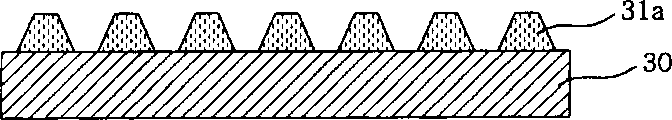
Fig. 3 a to 3c represents according to the process of prior art by Pendeo epitaxy method growing nitride semiconductive thin film.Referring to accompanying drawing, (Fig. 3 a) for growth regulation mononitride semiconductive thin film 31 on Sapphire Substrate 30.First nitride semiconductor thin film 31 of growth is etched into periodically bar pattern 31a (Fig. 3 b), and second nitride semiconductor thin film 32 utilizes periodically bar pattern 31a cross growth on Sapphire Substrate 30 (Fig. 3 c).
Therefore, the disruption potential density 32A of second nitride semiconductor thin film of cross growth is lowered.
As mentioned above, reduce the method for defective in the nitride-based semiconductor according to routine, be arranged on the zone that forms figure or be lowered from the defective of the nitride semiconductor thin film of the regional cross growth that forms insulation patterns, those are arranged in does not have the defectives in the zone that figure or insulating barrier figure form then to keep.Therefore, the problem that can not be improved that has whole crystal property.
That is to say that though defect concentration has reduced on the whole, the local or high or low property regional cycle ground of defect concentration exists.
Summary of the invention
Design of the present invention is to solve foregoing problems.Therefore, an object of the present invention is to provide a kind of low defective nitride semiconductor thin film and growing method thereof, wherein, the fabricating low-defect-density nitride semiconductor thin film is by forming the order grown buffer layer and first nitride semiconductor thin film on the substrate on it having groove, the high defect density regions of etching first nitride semiconductor thin film, the fabricating low-defect-density zone is formed periodically bar pattern, utilize this figure cross growth second nitride semiconductor thin film then and obtain.
Another object of the present invention provides a kind of low defective nitride semiconductor thin film and growing method thereof, wherein, the second fabricating low-defect-density nitride semiconductor thin film can form second nitride semiconductor thin film by utilizing the first fabricating low-defect-density nitride semiconductor thin film, thereby make second nitride semiconductor thin film can hang down the growth of the maintained state of defective, and (LEO) method form nitride semiconductor thin film with the zone at isolation masks figure place and integral body obtains by utilizing horizontal extension to grow nonparasitically upon another plant.
According to the first kind of scheme of the present invention that realizes above-mentioned purpose, a kind of method of the low defective nitride semiconductor thin film of growing is provided, comprising: the first step periodically forms on the whole surface of the substrate on it and forms resilient coating having strip groove; Second step, growth regulation mononitride semiconductive thin film on resilient coating; The 3rd step, on first nitride semiconductor thin film, form the isolation masks figure, so that the first nitride semiconductor thin film crested of on the area that strip groove forms, growing, and first nitride semiconductor thin film of growing on the area that does not have strip groove to form is exposed; In the 4th step, etching forms the periodicity bar pattern of the projection of first nitride semiconductor thin film by the zone of first nitride semiconductor thin film that has mask graph and expose, and removes the isolation masks figure from first nitride semiconductor thin film; And the 5th the step, utilize nitride semiconductor thin film figure cross growth second nitride semiconductor thin film.
According to the second kind of scheme of the present invention that realizes above-mentioned purpose, a kind of method of the low defective nitride semiconductor thin film of growing is provided, comprising: the first step periodically forms on the whole surface of the substrate on it and forms resilient coating having strip groove; Second step, growth regulation mononitride semiconductive thin film on resilient coating; The 3rd step, on first nitride semiconductor thin film, form the isolation masks figure, so that first nitride semiconductor thin film of growing on the area that strip groove forms is exposed, and the first nitride semiconductor thin film crested of on the area that does not have strip groove to form, growing; In the 4th step, utilize the isolation masks figure, cross growth second nitride semiconductor thin film on the zone of first nitride semiconductor thin film that exposes by the isolation masks figure.
According to the third scheme of the present invention that realizes above-mentioned purpose, a kind of method of the low defective nitride semiconductor thin film of growing is provided, comprising: the first step periodically forms at strip groove on the whole surface of the substrate on it and forms resilient coating; Second step, growth regulation mononitride semiconductive thin film on resilient coating; The 3rd step, on first nitride semiconductor thin film, form the isolation masks figure, so that the first nitride semiconductor thin film crested of on the area that strip groove forms, growing, and first nitride semiconductor thin film of growing on the area that does not have strip groove to form is exposed; In the 4th step, etching forms the first nitride semiconductor thin film figure, and removes the isolation masks figure from first nitride semiconductor thin film by the zone of first nitride semiconductor thin film of isolation masks figure exposure; In the 5th step, utilize nitride semiconductor thin film figure cross growth second nitride semiconductor thin film.
According to the 4th kind of scheme of the present invention that realizes above-mentioned purpose, a kind of method of the low defective nitride semiconductor thin film of growing is provided, comprising: the first step forms resilient coating on the whole surface of the substrate with groove; Second step, growth regulation mononitride semiconductive thin film on resilient coating; The 3rd step, on first nitride semiconductor thin film, form the isolation masks figure, so that first nitride semiconductor thin film of growing on the area that groove forms is exposed, and the first nitride semiconductor thin film crested of on the area that does not have groove to form, growing; And the 4th step, utilize the isolation masks figure, cross growth second nitride semiconductor thin film on by zone with first nitride semiconductor thin film that mask graph exposes.
According to the 5th kind of scheme of the present invention that realizes above-mentioned purpose, a kind of method of the low defective nitride semiconductor thin film of growing is provided, be included in and form groove on the substrate; Order forms the resilient coating and first nitride semiconductor thin film on the whole surface of substrate; The zone of first nitride semiconductor thin film the first nitride semiconductor thin film zone of etching on being formed on groove; And form second nitride semiconductor thin film.
The 6th kind of scheme of the present invention according to realizing above-mentioned purpose provides a kind of growth to hang down the defective nitride semiconductor thin film, comprising: have groove and form substrate on it; The resilient coating that on the whole surface of substrate, forms; Forming also on the resilient coating so that its zone that forms on groove forms first nitride semiconductor thin film of figure to the mode of upper process; Utilize second nitride semiconductor thin film of figure cross growth on first nitride semiconductor thin film of described first nitride semiconductor thin film.
The 7th kind of scheme of the present invention according to realizing above-mentioned purpose provides a kind of growth to hang down the defective nitride semiconductor thin film, comprising: have groove and form substrate on it; The resilient coating that on the whole surface of substrate, forms; First nitride semiconductor thin film that on resilient coating, forms; The isolation masks figure that on first nitride semiconductor thin film, forms; Second nitride semiconductor thin film of cross growth on by zone with first nitride semiconductor thin film that mask graph exposes.
Description of drawings
By the description below in conjunction with the preferred embodiment of accompanying drawing, above and other objects of the present invention, feature and advantage will become obviously, among the figure:
Utilization has the view that mask graph forms the process of the Sapphire Substrate growing nitride semiconductive thin film on it to Fig. 1 a to 1e according to prior art for expression;
Fig. 2 a to 2c for expression according to prior art by the grow nonparasitically upon another plant view of process of method growing nitride semiconductive thin film of horizontal extension;
Fig. 3 a to 3c passes through the view of the process of Pendeo epitaxy method growing nitride semiconductive thin film according to prior art for expression;
Fig. 4 a to 4f is the view of expression according to the process of the low defective nitride semiconductor thin film of growth of first embodiment of the invention;
Fig. 5 a to 5c is the view of expression according to the process of the low defective nitride semiconductor thin film of growth of second embodiment of the invention;
Fig. 6 a to 6c periodically forms the view of the process of strip groove on substrate according to the present invention for expression.
Embodiment
Below in conjunction with accompanying drawing the preferred embodiments of the present invention are done detailed description.
Fig. 4 a to 4f represents the process according to the low defective nitride semiconductor thin film of growth of first embodiment of the invention.Shown in Fig. 4 a, at first prepare to have strip groove 110a and form substrate 100 on it.Then, on the whole surface of substrate 100, form resilient coating 120 (Fig. 4 b).
Here, as previously mentioned, on substrate 100, form strip groove 110a, the groove of these each intervals form that is arranged in rows and columns.
And then resilient coating 120 is by Al
xGa
yIn
1-x-yThe stacked layered membrane on it of N (0≤x≤1,0≤y≤1,0≤x+y≤1) layer, SiN layer and previous layer is made.
In addition, substrate 100 can be made by being selected from the kind that comprises carborundum (SiC), sapphire, GaAs (GaAs) and gallium nitride (GaN).
Subsequently, on resilient coating 120, form first nitride semiconductor thin film 130 (Fig. 4 c).
At this moment, the zone that defect concentration is high (having more defective 201 in the zone of first nitride semiconductor thin film that forms on the zone that does not have strip groove to form) and the low zone (having less defects 202 in the zone of first nitride semiconductor thin film that forms on strip groove) of defect concentration alternately form in first nitride semiconductor thin film 130 of growth.
Then, shown in Fig. 4 d, on first nitride semiconductor thin film 130, form isolation masks figure 140, its generation type is, first nitride semiconductor thin film, 130 cresteds of on strip groove, growing, and first nitride semiconductor thin film 130 of growing on the zone that does not have strip groove to form is exposed.
That is to say that the fabricating low-defect-density zone of first nitride semiconductor thin film is by 140 cresteds of isolation masks figure, the high defect density regions of first nitride semiconductor thin film then is exposed.
Then, first nitride semiconductor thin film 130 that etching exposes by the isolation masks figure forms the first nitride semiconductor thin film figure 130a of bar shaped, and removes isolation masks figure 140 (Fig. 4 e).
Here, the high defect density regions of first nitride semiconductor thin film that exposes by isolation masks figure 140 is etched, and the fabricating low-defect-density zone of first nitride semiconductor thin film then forms the projection nitride semiconductor thin film of bar shaped.
Subsequently, by utilizing nitride semiconductor thin film figure 130a, cross growth second nitride semiconductor thin film 150 (Fig. 4 f).
Therefore, according to the first embodiment of the present invention, the preparation of fabricating low-defect-density nitride semiconductor thin film can be finished by following process, form at strip groove and to form the resilient coating and first nitride semiconductor thin film on the substrate on it, the high defect density regions of etching first nitride semiconductor thin film, the fabricating low-defect-density zone of first nitride semiconductor thin film is formed periodically bar pattern, utilize described figure cross growth second nitride semiconductor thin film.
Fig. 5 a to 5c represents the process according to the low defective nitride semiconductor thin film of second embodiment of the invention growth.The second embodiment of the present invention is to carry out after Fig. 4 of first embodiment of the invention c step.Promptly, shown in Fig. 5 a, on first nitride semiconductor thin film 130, form isolation masks figure 140, its generation type is, first nitride semiconductor thin film 130 of growing on strip groove is exposed, and first nitride semiconductor thin film, 130 cresteds of on the zone that does not have strip groove to form, growing.
Therefore, according to a second embodiment of the present invention, the fabricating low-defect-density zone of first nitride semiconductor thin film exposes, and covers and the high defect density regions of first nitride semiconductor thin film is insulated mask graph 140.
So the fabricating low-defect-density zone of first nitride semiconductor thin film is exposed with bar shaped.
Thereby, the cross growth (Fig. 5 b and 5c) on first nitride semiconductor thin film that exposes by the isolation masks figure of second nitride semiconductor thin film 150.
Therefore, according to a second embodiment of the present invention, form second nitride semiconductor thin film by first nitride semiconductor thin film that utilizes fabricating low-defect-density, thereby second nitride semiconductor thin film can hang down the maintained state growth of defective, and by utilize horizontal extension grow nonparasitically upon another plant (LEO) be nitride semiconductor thin film with the region growing at isolation masks figure place, the second fabricating low-defect-density nitride semiconductor thin film can obtain.Fig. 6 a to 6c represents according to the present invention periodically to form the process of strip groove on substrate.Isolation masks figure 110 is formed on the substrate 100, thus make substrate 100 can rule at interval d2 expose that (Fig. 6 a).
At this moment, the interval d of the substrate 100 that exposes by isolation masks figure 110 is preferably in 0.1 to 15.0 mu m range.
Then, the zone of the substrate 100 that exposes by isolation masks figure 110 is by with desired depth d3 etching (Fig. 6 b).
Here, the degree of depth of etched substrate 100 is preferably in 0.1 to 10 mu m range.
And then, if remove isolation masks figure 110, periodically form substrate 100 on it just obtain having strip groove.
In first and second embodiment of the present invention, groove can form polygon or circle.
And then, if the formation of resilient coating has the thickness less than the trench wall height, just so first nitride semiconductor thin film can the resilient coating of cross growth in groove on.Thereby, can further reduce defective.
According to aforesaid the present invention, the fabricating low-defect-density nitride semiconductor thin film can obtain by following process, on substrate, form groove, order forms the resilient coating and first nitride semiconductor thin film on the whole surface of substrate, the high defect density regions of etching first nitride semiconductor thin film, cross growth second nitride semiconductor thin film then.Therefore, the invention has the advantages that, can prepare the optical device or the electronic equipment of high efficiency, high-power and high reliability, and, also can obtain high throughput by utilizing the high crystallization nitride semiconductor thin film that in the equipment preparation, obtains.
Although expression of the present invention and description are carried out in conjunction with the preferred embodiments, be those skilled in the art will recognize in view of the above and can make various improvement and variation, and do not break away from the spirit and scope of the present invention.Also clearly, these improvement and variation can fall in the scope of the present invention that is limited by the accessory claim book.
Claims (20)
1, a kind of growing method of low defective nitride semiconductor thin film comprises:
The first step periodically forms on the whole surface of the substrate on it and forms resilient coating having strip groove;
Second step, growth regulation mononitride semiconductive thin film on resilient coating;
The 3rd step, on first nitride semiconductor thin film, form the isolation masks figure, so that the first nitride semiconductor thin film crested of on the area that strip groove forms, growing, and first nitride semiconductor thin film of growing on the area that does not have strip groove to form is exposed;
The 4th step, the zone of first nitride semiconductor thin film that etching is exposed by the isolation masks figure, the projection that forms first nitride semiconductor thin film is bar pattern periodically, and removes the isolation masks figure from first nitride semiconductor thin film; And
In the 5th step, utilize nitride semiconductor thin film figure cross growth second nitride semiconductor thin film.
2, a kind of growing method of low defective nitride semiconductor thin film comprises:
The first step periodically forms on the whole surface of the substrate on it and forms resilient coating having strip groove;
Second step, growth regulation mononitride semiconductive thin film on resilient coating;
The 3rd step, on first nitride semiconductor thin film, form the isolation masks figure, so that first nitride semiconductor thin film of growing on the area that strip groove forms is exposed, and the first nitride semiconductor thin film crested of on the area that does not have strip groove to form, growing; And
In the 4th step, utilize the isolation masks figure, cross growth second nitride semiconductor thin film on the zone of first nitride semiconductor thin film that exposes by the isolation masks figure.
3, method according to claim 1 and 2 is characterized in that, wherein has the preparation process that strip groove periodically forms the substrate on it to be:
On substrate, form the isolation masks figure, make substrate with rule (d2) exposure at interval;
With the substrate of desired depth (d3) etching by the exposure of isolation masks figure; And
Remove the isolation masks figure from substrate.
4, method as claimed in claim 3 is characterized in that, wherein said interval (d2) is in the scope of 0.1 to 15.0 μ m.
5, method as claimed in claim 3 is characterized in that, the wherein said etch substrate degree of depth is in the scope of 0.1 to 10.0 μ m.
6, method as claimed in claim 3 is characterized in that, the preparation material of wherein said substrate is selected from the kind that comprises carborundum (SiC), sapphire, GaAs (GaAs) and gallium nitride (GaN).
7, method as claimed in claim 1 or 2 is characterized in that, wherein said resilient coating is by Al
xGa
yIn
1-x-yN (0≤x≤1,0≤y≤1,0≤x+y≤1) layer, SiN layer and each stacked layered membrane of putting on it are made.
8, method as claimed in claim 1 or 2, it is characterized in that, wherein after second step, first nitride semiconductor thin film has higher defect concentration on the zone that does not have strip groove to form, and has than fabricating low-defect-density on the zone that has strip groove to form.
9, method as claimed in claim 8 is characterized in that, wherein the isolation masks figure is exposed the fabricating low-defect-density zone crested of first nitride semiconductor thin film and the high defect density regions of first nitride semiconductor thin film.
10, a kind of growing method of low defective nitride semiconductor thin film comprises:
The first step periodically forms at strip groove on the whole surface of the substrate on it and forms resilient coating;
Second step, growth regulation mononitride semiconductive thin film on resilient coating;
The 3rd step, on first nitride semiconductor thin film, form the isolation masks figure, so that the first nitride semiconductor thin film crested of on the zone that strip groove forms, growing, and first nitride semiconductor thin film of growing on the area that does not have strip groove to form is exposed;
In the 4th step, etching forms the first nitride semiconductor thin film figure by the zone of first nitride semiconductor thin film of isolation masks figure exposure, and removes the isolation masks figure from first nitride semiconductor thin film; And
In the 5th step, utilize nitride semiconductor thin film figure cross growth second nitride semiconductor thin film.
11, a kind of growing method of low defective nitride semiconductor thin film comprises:
The first step forms resilient coating on the whole surface of the substrate with groove;
Second step, growth regulation mononitride semiconductive thin film on resilient coating;
The 3rd step, on first nitride semiconductor thin film, form the isolation masks figure, so that first nitride semiconductor thin film of growing on the zone of the substrate that groove forms is exposed, and the first nitride semiconductor thin film crested of on the zone of the substrate that does not have groove to form, growing; And
In the 4th step, utilize the isolation masks figure, cross growth second nitride semiconductor thin film on the zone of first nitride semiconductor thin film that exposes by the isolation masks figure.
12, as claim 10 or 11 described methods, it is characterized in that wherein said groove periodically forms.
As claim 10 or 11 described methods, it is characterized in that 13, wherein said groove is polygon or circle.
14,, it is characterized in that wherein said resilient coating forms in the mode that has less than the thickness of trench wall height as claim 10 or 11 described methods.
15, as claim 10 or 11 described methods, it is characterized in that wherein said resilient coating is by Al
xGa
yIn
1-x-yN (0≤x≤1,0≤y≤1,0≤x+y≤1) layer, SiN layer and each stacked layered membrane of putting on it are made.
16, a kind of growing method of low defective nitride semiconductor thin film comprises the following steps:
On substrate, form groove;
Order forms the resilient coating and first nitride semiconductor thin film on the whole surface of substrate;
Etching is except that the zone of first nitride semiconductor thin film the first nitride semiconductor thin film zone that forms on the groove;
Form second nitride semiconductor thin film.
17, a kind of low defective nitride semiconductor thin film comprises:
Have groove and form substrate on it;
The resilient coating that on the whole surface of described substrate, forms;
In formation on the resilient coating and so that its zone that forms on groove forms first nitride semiconductor thin film of figure to the upper process mode; And
Utilize second nitride semiconductor thin film of figure cross growth on first nitride semiconductor thin film of described first nitride semiconductor thin film.
18, a kind of low defective nitride semiconductor thin film comprises:
Have groove and form substrate on it;
The resilient coating that on the whole surface of described substrate, forms;
First nitride semiconductor thin film that on resilient coating, forms;
The isolation masks figure that on first nitride semiconductor thin film, forms; And
Second nitride semiconductor thin film of cross growth on by zone with first nitride semiconductor thin film that mask graph exposes.
19,, it is characterized in that wherein said resilient coating forms in the mode that has less than the thickness of the height of trench wall as claim 17 or 18 described nitride semiconductor thin films.
20, nitride semiconductor thin film as claimed in claim 18, it is characterized in that, the generation type of wherein said isolation masks figure is, first nitride semiconductor thin film of growing on the area that groove forms is exposed, and the first nitride semiconductor thin film crested of on the area that does not have groove to form, growing.
Applications Claiming Priority (2)
| Application Number | Priority Date | Filing Date | Title |
|---|---|---|---|
| KR1020030101283 | 2003-12-31 | ||
| KR10-2003-0101283A KR100512580B1 (en) | 2003-12-31 | 2003-12-31 | Method of growing nitride semiconductor thin film having small defects |
Publications (1)
| Publication Number | Publication Date |
|---|---|
| CN1638041A true CN1638041A (en) | 2005-07-13 |
Family
ID=34567865
Family Applications (1)
| Application Number | Title | Priority Date | Filing Date |
|---|---|---|---|
| CNA2004101031516A Pending CN1638041A (en) | 2003-12-31 | 2004-12-31 | Nitride semiconductor thin film having fewer defects and method of growing the same |
Country Status (5)
| Country | Link |
|---|---|
| US (2) | US7198971B2 (en) |
| EP (1) | EP1551056B1 (en) |
| JP (1) | JP4614125B2 (en) |
| KR (1) | KR100512580B1 (en) |
| CN (1) | CN1638041A (en) |
Cited By (4)
| Publication number | Priority date | Publication date | Assignee | Title |
|---|---|---|---|---|
| CN101587831B (en) * | 2008-05-19 | 2013-01-16 | 展晶科技(深圳)有限公司 | Semiconductor component structure and method for manufacturing semiconductor component |
| CN107548517A (en) * | 2015-05-15 | 2018-01-05 | 欧司朗光电半导体有限公司 | Method for manufacturing nitride compound semiconductor device |
| CN109616560A (en) * | 2018-11-21 | 2019-04-12 | 江西兆驰半导体有限公司 | A kind of compound substrate suitable for nitride epitaxial layer growth |
| WO2021237528A1 (en) * | 2020-05-27 | 2021-12-02 | 苏州晶湛半导体有限公司 | Group iii nitride structure and preparation method therefor |
Families Citing this family (24)
| Publication number | Priority date | Publication date | Assignee | Title |
|---|---|---|---|---|
| KR100512580B1 (en) * | 2003-12-31 | 2005-09-06 | 엘지전자 주식회사 | Method of growing nitride semiconductor thin film having small defects |
| JP5013661B2 (en) * | 2004-03-31 | 2012-08-29 | 三洋電機株式会社 | Nitride semiconductor device manufacturing method and nitride semiconductor device |
| KR100679610B1 (en) * | 2006-01-16 | 2007-02-06 | 삼성전자주식회사 | Method of manufacturing a thin film layer of single crystal structure |
| TWI304278B (en) * | 2006-06-16 | 2008-12-11 | Ind Tech Res Inst | Semiconductor emitting device substrate and method of fabricating the same |
| TW200805452A (en) * | 2006-07-06 | 2008-01-16 | Nat Univ Chung Hsing | Method of making a low-defect-density epitaxial substrate and the product made therefrom |
| TWI464899B (en) * | 2008-05-09 | 2014-12-11 | Advanced Optoelectronic Tech | A method for manufacturing a semiconductor element |
| US8377796B2 (en) | 2008-08-11 | 2013-02-19 | Taiwan Semiconductor Manufacturing Company, Ltd. | III-V compound semiconductor epitaxy from a non-III-V substrate |
| US8803189B2 (en) * | 2008-08-11 | 2014-08-12 | Taiwan Semiconductor Manufacturing Company, Ltd. | III-V compound semiconductor epitaxy using lateral overgrowth |
| TW201029073A (en) * | 2009-01-21 | 2010-08-01 | Univ Nat Chunghsing | Epitaxial wafer with low surface defect density |
| KR101461684B1 (en) * | 2009-02-24 | 2014-11-20 | 엘지전자 주식회사 | Nitride semiconductor light emitting device and method for manufacturing the same |
| US8039371B2 (en) * | 2009-07-01 | 2011-10-18 | International Business Machines Corporation | Reduced defect semiconductor-on-insulator hetero-structures |
| US8375349B2 (en) | 2009-09-02 | 2013-02-12 | Taiwan Semiconductor Manufacturing Company, Ltd. | Method for constant power density scaling |
| CN102054852A (en) * | 2009-10-28 | 2011-05-11 | 展晶科技(深圳)有限公司 | Light-emitting diode and manufacturing method thereof |
| US8759203B2 (en) * | 2009-11-17 | 2014-06-24 | Taiwan Semiconductor Manufacturing Company, Ltd. | Growing III-V compound semiconductors from trenches filled with intermediate layers |
| US8501597B2 (en) * | 2010-07-30 | 2013-08-06 | Academia Sinica | Method for fabricating group III-nitride semiconductor |
| TWI451480B (en) * | 2010-10-08 | 2014-09-01 | Academia Sinica | Method for fabricating group iii-nitride semiconductor |
| FR3022563B1 (en) * | 2014-06-23 | 2016-07-15 | Univ Paris Xiii Paris-Nord Villetaneuse | METHOD FOR FORMING A MONOCRYSTAL OF MATERIAL FROM A MONOCRYSTALLINE SUBSTRATE |
| US10366883B2 (en) | 2014-07-30 | 2019-07-30 | Hewlett Packard Enterprise Development Lp | Hybrid multilayer device |
| US10658177B2 (en) * | 2015-09-03 | 2020-05-19 | Hewlett Packard Enterprise Development Lp | Defect-free heterogeneous substrates |
| US10586847B2 (en) | 2016-01-15 | 2020-03-10 | Hewlett Packard Enterprise Development Lp | Multilayer device |
| US11088244B2 (en) | 2016-03-30 | 2021-08-10 | Hewlett Packard Enterprise Development Lp | Devices having substrates with selective airgap regions |
| US10381801B1 (en) | 2018-04-26 | 2019-08-13 | Hewlett Packard Enterprise Development Lp | Device including structure over airgap |
| CN113555283B (en) * | 2020-04-24 | 2024-04-05 | 江苏鲁汶仪器股份有限公司 | Method for etching heterojunction of GaN-based high-electron-mobility transistor |
| CN112382709B (en) * | 2020-12-03 | 2022-02-25 | 至芯半导体(杭州)有限公司 | Manufacturing method of anti-crack AlN epitaxial layer |
Family Cites Families (17)
| Publication number | Priority date | Publication date | Assignee | Title |
|---|---|---|---|---|
| EP0942459B1 (en) * | 1997-04-11 | 2012-03-21 | Nichia Corporation | Method of growing nitride semiconductors |
| US6608327B1 (en) * | 1998-02-27 | 2003-08-19 | North Carolina State University | Gallium nitride semiconductor structure including laterally offset patterned layers |
| US6265289B1 (en) * | 1998-06-10 | 2001-07-24 | North Carolina State University | Methods of fabricating gallium nitride semiconductor layers by lateral growth from sidewalls into trenches, and gallium nitride semiconductor structures fabricated thereby |
| JP4005701B2 (en) * | 1998-06-24 | 2007-11-14 | シャープ株式会社 | Method of forming nitrogen compound semiconductor film and nitrogen compound semiconductor element |
| WO2000055893A1 (en) * | 1999-03-17 | 2000-09-21 | Mitsubishi Cable Industries, Ltd. | Semiconductor base and its manufacturing method, and semiconductor crystal manufacturing method |
| JP3555500B2 (en) * | 1999-05-21 | 2004-08-18 | 豊田合成株式会社 | Group III nitride semiconductor and method of manufacturing the same |
| US6812053B1 (en) * | 1999-10-14 | 2004-11-02 | Cree, Inc. | Single step pendeo- and lateral epitaxial overgrowth of Group III-nitride epitaxial layers with Group III-nitride buffer layer and resulting structures |
| EP1104031B1 (en) * | 1999-11-15 | 2012-04-11 | Panasonic Corporation | Nitride semiconductor laser diode and method of fabricating the same |
| US6521514B1 (en) * | 1999-11-17 | 2003-02-18 | North Carolina State University | Pendeoepitaxial methods of fabricating gallium nitride semiconductor layers on sapphire substrates |
| JP4547746B2 (en) * | 1999-12-01 | 2010-09-22 | ソニー株式会社 | Method for producing crystal of nitride III-V compound |
| JP4432180B2 (en) * | 1999-12-24 | 2010-03-17 | 豊田合成株式会社 | Group III nitride compound semiconductor manufacturing method, group III nitride compound semiconductor device, and group III nitride compound semiconductor |
| US6403451B1 (en) * | 2000-02-09 | 2002-06-11 | Noerh Carolina State University | Methods of fabricating gallium nitride semiconductor layers on substrates including non-gallium nitride posts |
| KR20020084194A (en) * | 2000-03-14 | 2002-11-04 | 도요다 고세이 가부시키가이샤 | Production method of iii nitride compound semiconductor and iii nitride compound semiconductor element |
| US6627974B2 (en) * | 2000-06-19 | 2003-09-30 | Nichia Corporation | Nitride semiconductor substrate and method for manufacturing the same, and nitride semiconductor device using nitride semiconductor substrate |
| JP3679720B2 (en) * | 2001-02-27 | 2005-08-03 | 三洋電機株式会社 | Nitride semiconductor device and method for forming nitride semiconductor |
| EP1276140A3 (en) * | 2001-07-04 | 2007-10-24 | FUJIFILM Corporation | Substrate including wide low-defect region for use in semiconductor element |
| KR100512580B1 (en) * | 2003-12-31 | 2005-09-06 | 엘지전자 주식회사 | Method of growing nitride semiconductor thin film having small defects |
-
2003
- 2003-12-31 KR KR10-2003-0101283A patent/KR100512580B1/en not_active IP Right Cessation
-
2004
- 2004-12-28 JP JP2004380053A patent/JP4614125B2/en not_active Expired - Fee Related
- 2004-12-29 US US11/023,540 patent/US7198971B2/en not_active Expired - Fee Related
- 2004-12-30 EP EP04031027.8A patent/EP1551056B1/en not_active Expired - Fee Related
- 2004-12-31 CN CNA2004101031516A patent/CN1638041A/en active Pending
-
2007
- 2007-03-20 US US11/725,498 patent/US20070190678A1/en not_active Abandoned
Cited By (5)
| Publication number | Priority date | Publication date | Assignee | Title |
|---|---|---|---|---|
| CN101587831B (en) * | 2008-05-19 | 2013-01-16 | 展晶科技(深圳)有限公司 | Semiconductor component structure and method for manufacturing semiconductor component |
| CN107548517A (en) * | 2015-05-15 | 2018-01-05 | 欧司朗光电半导体有限公司 | Method for manufacturing nitride compound semiconductor device |
| CN107548517B (en) * | 2015-05-15 | 2020-10-30 | 欧司朗光电半导体有限公司 | Method for manufacturing nitride compound semiconductor device |
| CN109616560A (en) * | 2018-11-21 | 2019-04-12 | 江西兆驰半导体有限公司 | A kind of compound substrate suitable for nitride epitaxial layer growth |
| WO2021237528A1 (en) * | 2020-05-27 | 2021-12-02 | 苏州晶湛半导体有限公司 | Group iii nitride structure and preparation method therefor |
Also Published As
| Publication number | Publication date |
|---|---|
| JP4614125B2 (en) | 2011-01-19 |
| US20050139857A1 (en) | 2005-06-30 |
| KR20050069315A (en) | 2005-07-05 |
| EP1551056A3 (en) | 2006-06-28 |
| KR100512580B1 (en) | 2005-09-06 |
| US7198971B2 (en) | 2007-04-03 |
| EP1551056A2 (en) | 2005-07-06 |
| US20070190678A1 (en) | 2007-08-16 |
| EP1551056B1 (en) | 2015-02-11 |
| JP2005197721A (en) | 2005-07-21 |
Similar Documents
| Publication | Publication Date | Title |
|---|---|---|
| CN1638041A (en) | Nitride semiconductor thin film having fewer defects and method of growing the same | |
| CN1189920C (en) | Method for producing group III nitride compound semiconductor and group III nitride compound semiconductor device | |
| KR100735496B1 (en) | Method for forming the vertically structured gan type light emitting diode device | |
| EP1936668B1 (en) | Nitride semiconductor substrate and manufacturing method thereof | |
| US20180151359A1 (en) | Growing III-V Compound Semiconductors from Trenches Filled with Intermediate Layers | |
| CN1157804C (en) | Nitride semiconductor device and its manufacturing method | |
| CN1641835A (en) | High quality nitride semiconductor thin film and method for growing the same | |
| CN1183577C (en) | Single step pendeo-and Lateral overgrowth of group III-nitride layers | |
| KR100769727B1 (en) | Forming method for surface unevenness and manufacturing method for gan type led device using thereof | |
| CN101866880B (en) | Method for separating base plate and semiconductor layer | |
| CN102576780B (en) | High-quality non-polar/semi-polar semiconductor element on an unevenly patterned substrate and a production method therefor | |
| CN1649090A (en) | Nitride semiconductor thin film and method for growing the same | |
| CN103548154A (en) | Semiconductor devices and fabrication methods | |
| CN1820353A (en) | Growth method of nitride semiconductor epitaxial layers | |
| CN1731587A (en) | Vertical type wide bandgap semiconductor device structure and making method | |
| TW201133935A (en) | Semiconductor light-emitting device | |
| CN101728244A (en) | Method for blocking dislocation defects of semiconductor | |
| US9299561B2 (en) | Method for fabricating nitride semiconductor thin film and method for fabricating nitride semiconductor device using the same | |
| JP2010171427A (en) | Epitaxial structure having low defect density, and production process of the same | |
| KR100454907B1 (en) | Nitride Semiconductor substrate and method for manufacturing the same | |
| KR100816490B1 (en) | Light emitting diode and method for manufacturing the same | |
| KR101901932B1 (en) | Substrate having heterostructure, nitride-based semiconductor light emitting device and method for manufacturing the same | |
| KR101173985B1 (en) | Method of manufacturing a substrate | |
| US10229976B2 (en) | Compound semiconductor film structure | |
| CN1797712A (en) | Epitaxy base plate in use for solid-state semiconductor device, solid-state semiconductor device, and preparation method |
Legal Events
| Date | Code | Title | Description |
|---|---|---|---|
| C06 | Publication | ||
| PB01 | Publication | ||
| C10 | Entry into substantive examination | ||
| SE01 | Entry into force of request for substantive examination | ||
| C02 | Deemed withdrawal of patent application after publication (patent law 2001) | ||
| WD01 | Invention patent application deemed withdrawn after publication |