CN1490635A - Optical component and producing method thereof, lenticule substrate and producing method thereof, displaying device, camera component - Google Patents
Optical component and producing method thereof, lenticule substrate and producing method thereof, displaying device, camera component Download PDFInfo
- Publication number
- CN1490635A CN1490635A CNA031569722A CN03156972A CN1490635A CN 1490635 A CN1490635 A CN 1490635A CN A031569722 A CNA031569722 A CN A031569722A CN 03156972 A CN03156972 A CN 03156972A CN 1490635 A CN1490635 A CN 1490635A
- Authority
- CN
- China
- Prior art keywords
- optical component
- base component
- optics
- component
- manufacture method
- Prior art date
- Legal status (The legal status is an assumption and is not a legal conclusion. Google has not performed a legal analysis and makes no representation as to the accuracy of the status listed.)
- Pending
Links
- 230000003287 optical effect Effects 0.000 title claims abstract description 225
- 239000000758 substrate Substances 0.000 title claims abstract description 95
- 238000000034 method Methods 0.000 title claims description 109
- 238000004519 manufacturing process Methods 0.000 claims abstract description 71
- 239000000463 material Substances 0.000 claims description 43
- 239000011159 matrix material Substances 0.000 claims description 41
- 239000011347 resin Substances 0.000 claims description 27
- 229920005989 resin Polymers 0.000 claims description 27
- 230000010287 polarization Effects 0.000 claims description 10
- 230000001154 acute effect Effects 0.000 claims description 8
- 239000008393 encapsulating agent Substances 0.000 claims description 7
- 238000003384 imaging method Methods 0.000 claims description 7
- 230000015572 biosynthetic process Effects 0.000 description 35
- 238000005755 formation reaction Methods 0.000 description 35
- 230000001681 protective effect Effects 0.000 description 13
- 238000005530 etching Methods 0.000 description 11
- 230000000694 effects Effects 0.000 description 8
- 230000009471 action Effects 0.000 description 7
- 239000011521 glass Substances 0.000 description 7
- 208000034189 Sclerosis Diseases 0.000 description 6
- 238000010586 diagram Methods 0.000 description 5
- 229920001721 polyimide Polymers 0.000 description 5
- 230000008859 change Effects 0.000 description 4
- 239000007788 liquid Substances 0.000 description 4
- 239000000853 adhesive Substances 0.000 description 3
- 230000001070 adhesive effect Effects 0.000 description 3
- 238000005422 blasting Methods 0.000 description 3
- 238000000576 coating method Methods 0.000 description 3
- 238000001723 curing Methods 0.000 description 3
- 238000005520 cutting process Methods 0.000 description 3
- 239000004973 liquid crystal related substance Substances 0.000 description 3
- 239000009719 polyimide resin Substances 0.000 description 3
- 238000012545 processing Methods 0.000 description 3
- 230000007261 regionalization Effects 0.000 description 3
- 229920001187 thermosetting polymer Polymers 0.000 description 3
- XKRFYHLGVUSROY-UHFFFAOYSA-N Argon Chemical compound [Ar] XKRFYHLGVUSROY-UHFFFAOYSA-N 0.000 description 2
- IJGRMHOSHXDMSA-UHFFFAOYSA-N Atomic nitrogen Chemical compound N#N IJGRMHOSHXDMSA-UHFFFAOYSA-N 0.000 description 2
- 239000004642 Polyimide Substances 0.000 description 2
- 238000005516 engineering process Methods 0.000 description 2
- 239000003822 epoxy resin Substances 0.000 description 2
- 239000007789 gas Substances 0.000 description 2
- 238000012856 packing Methods 0.000 description 2
- 229920000647 polyepoxide Polymers 0.000 description 2
- 239000007787 solid Substances 0.000 description 2
- 238000007669 thermal treatment Methods 0.000 description 2
- 238000009736 wetting Methods 0.000 description 2
- WNEODWDFDXWOLU-QHCPKHFHSA-N 3-[3-(hydroxymethyl)-4-[1-methyl-5-[[5-[(2s)-2-methyl-4-(oxetan-3-yl)piperazin-1-yl]pyridin-2-yl]amino]-6-oxopyridin-3-yl]pyridin-2-yl]-7,7-dimethyl-1,2,6,8-tetrahydrocyclopenta[3,4]pyrrolo[3,5-b]pyrazin-4-one Chemical compound C([C@@H](N(CC1)C=2C=NC(NC=3C(N(C)C=C(C=3)C=3C(=C(N4C(C5=CC=6CC(C)(C)CC=6N5CC4)=O)N=CC=3)CO)=O)=CC=2)C)N1C1COC1 WNEODWDFDXWOLU-QHCPKHFHSA-N 0.000 description 1
- 239000004925 Acrylic resin Substances 0.000 description 1
- 229920000178 Acrylic resin Polymers 0.000 description 1
- KRHYYFGTRYWZRS-UHFFFAOYSA-N Fluorane Chemical compound F KRHYYFGTRYWZRS-UHFFFAOYSA-N 0.000 description 1
- 229910001218 Gallium arsenide Inorganic materials 0.000 description 1
- XUIMIQQOPSSXEZ-UHFFFAOYSA-N Silicon Chemical compound [Si] XUIMIQQOPSSXEZ-UHFFFAOYSA-N 0.000 description 1
- 239000002390 adhesive tape Substances 0.000 description 1
- 239000012670 alkaline solution Substances 0.000 description 1
- 229910052786 argon Inorganic materials 0.000 description 1
- 238000007664 blowing Methods 0.000 description 1
- 239000011248 coating agent Substances 0.000 description 1
- 230000008878 coupling Effects 0.000 description 1
- 238000010168 coupling process Methods 0.000 description 1
- 238000005859 coupling reaction Methods 0.000 description 1
- 238000009826 distribution Methods 0.000 description 1
- 238000001312 dry etching Methods 0.000 description 1
- 238000007429 general method Methods 0.000 description 1
- 238000013007 heat curing Methods 0.000 description 1
- 229960002050 hydrofluoric acid Drugs 0.000 description 1
- 230000006872 improvement Effects 0.000 description 1
- 239000011261 inert gas Substances 0.000 description 1
- 238000010884 ion-beam technique Methods 0.000 description 1
- 238000003475 lamination Methods 0.000 description 1
- 239000011344 liquid material Substances 0.000 description 1
- 238000001459 lithography Methods 0.000 description 1
- 238000012423 maintenance Methods 0.000 description 1
- 238000003801 milling Methods 0.000 description 1
- 238000012986 modification Methods 0.000 description 1
- 230000004048 modification Effects 0.000 description 1
- 229910052757 nitrogen Inorganic materials 0.000 description 1
- NJPPVKZQTLUDBO-UHFFFAOYSA-N novaluron Chemical compound C1=C(Cl)C(OC(F)(F)C(OC(F)(F)F)F)=CC=C1NC(=O)NC(=O)C1=C(F)C=CC=C1F NJPPVKZQTLUDBO-UHFFFAOYSA-N 0.000 description 1
- 239000013307 optical fiber Substances 0.000 description 1
- 239000002245 particle Substances 0.000 description 1
- 238000003825 pressing Methods 0.000 description 1
- QQONPFPTGQHPMA-UHFFFAOYSA-N propylene Natural products CC=C QQONPFPTGQHPMA-UHFFFAOYSA-N 0.000 description 1
- 125000004805 propylene group Chemical group [H]C([H])([H])C([H])([*:1])C([H])([H])[*:2] 0.000 description 1
- 239000011241 protective layer Substances 0.000 description 1
- 239000004065 semiconductor Substances 0.000 description 1
- 229910052710 silicon Inorganic materials 0.000 description 1
- 239000010703 silicon Substances 0.000 description 1
- 239000000243 solution Substances 0.000 description 1
- 238000001039 wet etching Methods 0.000 description 1
Images


Classifications
-
- H—ELECTRICITY
- H01—ELECTRIC ELEMENTS
- H01L—SEMICONDUCTOR DEVICES NOT COVERED BY CLASS H10
- H01L27/00—Devices consisting of a plurality of semiconductor or other solid-state components formed in or on a common substrate
- H01L27/14—Devices consisting of a plurality of semiconductor or other solid-state components formed in or on a common substrate including semiconductor components sensitive to infrared radiation, light, electromagnetic radiation of shorter wavelength or corpuscular radiation and specially adapted either for the conversion of the energy of such radiation into electrical energy or for the control of electrical energy by such radiation
-
- G—PHYSICS
- G02—OPTICS
- G02B—OPTICAL ELEMENTS, SYSTEMS OR APPARATUS
- G02B7/00—Mountings, adjusting means, or light-tight connections, for optical elements
- G02B7/02—Mountings, adjusting means, or light-tight connections, for optical elements for lenses
- G02B7/025—Mountings, adjusting means, or light-tight connections, for optical elements for lenses using glue
-
- B—PERFORMING OPERATIONS; TRANSPORTING
- B29—WORKING OF PLASTICS; WORKING OF SUBSTANCES IN A PLASTIC STATE IN GENERAL
- B29D—PRODUCING PARTICULAR ARTICLES FROM PLASTICS OR FROM SUBSTANCES IN A PLASTIC STATE
- B29D11/00—Producing optical elements, e.g. lenses or prisms
- B29D11/00009—Production of simple or compound lenses
- B29D11/00278—Lenticular sheets
-
- B—PERFORMING OPERATIONS; TRANSPORTING
- B29—WORKING OF PLASTICS; WORKING OF SUBSTANCES IN A PLASTIC STATE IN GENERAL
- B29D—PRODUCING PARTICULAR ARTICLES FROM PLASTICS OR FROM SUBSTANCES IN A PLASTIC STATE
- B29D11/00—Producing optical elements, e.g. lenses or prisms
- B29D11/00009—Production of simple or compound lenses
- B29D11/00365—Production of microlenses
-
- B—PERFORMING OPERATIONS; TRANSPORTING
- B41—PRINTING; LINING MACHINES; TYPEWRITERS; STAMPS
- B41J—TYPEWRITERS; SELECTIVE PRINTING MECHANISMS, i.e. MECHANISMS PRINTING OTHERWISE THAN FROM A FORME; CORRECTION OF TYPOGRAPHICAL ERRORS
- B41J2/00—Typewriters or selective printing mechanisms characterised by the printing or marking process for which they are designed
- B41J2/005—Typewriters or selective printing mechanisms characterised by the printing or marking process for which they are designed characterised by bringing liquid or particles selectively into contact with a printing material
- B41J2/01—Ink jet
-
- G—PHYSICS
- G02—OPTICS
- G02B—OPTICAL ELEMENTS, SYSTEMS OR APPARATUS
- G02B3/00—Simple or compound lenses
- G02B3/0006—Arrays
- G02B3/0012—Arrays characterised by the manufacturing method
-
- G—PHYSICS
- G02—OPTICS
- G02B—OPTICAL ELEMENTS, SYSTEMS OR APPARATUS
- G02B3/00—Simple or compound lenses
- G02B3/0006—Arrays
- G02B3/0037—Arrays characterized by the distribution or form of lenses
- G02B3/0056—Arrays characterized by the distribution or form of lenses arranged along two different directions in a plane, e.g. honeycomb arrangement of lenses
-
- G—PHYSICS
- G02—OPTICS
- G02B—OPTICAL ELEMENTS, SYSTEMS OR APPARATUS
- G02B7/00—Mountings, adjusting means, or light-tight connections, for optical elements
- G02B7/02—Mountings, adjusting means, or light-tight connections, for optical elements for lenses
- G02B7/027—Mountings, adjusting means, or light-tight connections, for optical elements for lenses the lens being in the form of a sphere or ball
-
- H—ELECTRICITY
- H01—ELECTRIC ELEMENTS
- H01L—SEMICONDUCTOR DEVICES NOT COVERED BY CLASS H10
- H01L23/00—Details of semiconductor or other solid state devices
-
- B—PERFORMING OPERATIONS; TRANSPORTING
- B41—PRINTING; LINING MACHINES; TYPEWRITERS; STAMPS
- B41J—TYPEWRITERS; SELECTIVE PRINTING MECHANISMS, i.e. MECHANISMS PRINTING OTHERWISE THAN FROM A FORME; CORRECTION OF TYPOGRAPHICAL ERRORS
- B41J2202/00—Embodiments of or processes related to ink-jet or thermal heads
- B41J2202/01—Embodiments of or processes related to ink-jet heads
- B41J2202/09—Ink jet technology used for manufacturing optical filters
-
- G—PHYSICS
- G02—OPTICS
- G02B—OPTICAL ELEMENTS, SYSTEMS OR APPARATUS
- G02B3/00—Simple or compound lenses
- G02B3/0006—Arrays
- G02B3/0075—Arrays characterized by non-optical structures, e.g. having integrated holding or alignment means
Landscapes
- Physics & Mathematics (AREA)
- Engineering & Computer Science (AREA)
- General Physics & Mathematics (AREA)
- Optics & Photonics (AREA)
- Manufacturing & Machinery (AREA)
- Ophthalmology & Optometry (AREA)
- Health & Medical Sciences (AREA)
- Mechanical Engineering (AREA)
- Power Engineering (AREA)
- Condensed Matter Physics & Semiconductors (AREA)
- Computer Hardware Design (AREA)
- Microelectronics & Electronic Packaging (AREA)
- Electromagnetism (AREA)
- Optical Elements Other Than Lenses (AREA)
- Casting Or Compression Moulding Of Plastics Or The Like (AREA)
Abstract
The invention provides an optical component whose siting, shape and size are well controlled and a method of manufacturing such an optical component. The optical component of the present invention includes a base member disposed on a substrate, and an optical member disposed on the top surface of the base member.
Description
Technical field
The present invention relates to the optics and the manufacture method thereof of a kind of control setting well position, shape and size.The invention still further relates to a kind of lenticular substrate and manufacture method, display device and imaging apparatus.
Background technology
For example, as the manufacture method of optical components such as known a kind of lens, be on matrix (substrate), to shoot out the drop that constitutes by fluent material, make its curing then.But, in this method,, restricted the shape of optical component owing to the contact angle between drop and the matrix, therefore, be difficult to obtain the optical component that focal length is adjusted appropriateness.
Also have, for example, form the method (for example referring to patent documentation 1 and patent documentation 2) of the optical component of the shape that requires by adjusting the wellability of matrix surface.
(patent documentation 1) Jap.P. 1990-165932 number bulletin
(patent documentation 2) Jap.P. 2000-280367 number bulletin
Yet this method can't enough critically be controlled shape, the size of optical component and the position is set.
Summary of the invention
The object of the present invention is to provide the optics and the manufacture method thereof of a kind of control setting well position, shape and size.
The present invention also aims to provide a kind of lenticular substrate and the manufacture method thereof that position, shape and size are set that can control lens well; And display device and the imaging apparatus of being furnished with this lenticule substrate.
1. optics
Optics of the present invention comprises: the base component that is provided with on matrix; And the optical component that is provided with at the upper surface of described base component.
Here said " matrix " is meant a kind of object of face on its face described base component can be set.No matter described as long as described base component can be set, be that plane or curved surface can.Therefore, only require to have such face, there is no particular limitation to the shape of described matrix itself.And described base component also can be arranged to an integral body with matrix.
In addition, so-called " base component " is meant the member with upper surface that described optical component can be set, and so-called " upper surface of base component " is meant the one side that described optical component is set.No matter the upper surface of described base component as long as described optical component can be set, is that plane or curved surface can.So-called " optical component " is meant to have the character that can change light or the member of direct of travel function.
According to the present invention, owing to have an above-mentioned formation, therefore shape by the described base component upper surface of control and height etc. just can obtain to comprise the optics of having controlled the optical component that position, shape and size are set well.Details will explanation in this enforcement.
Optics of the present invention can be taked the described mode in following (1)~(10).
(1) described base component can be made of the material that can see through specific wavelength light.
Here said " seeing through ", be meant that the light that incides on the described base component penetrates from this base component again, but ' seeing through ' not only includes the situation that the light that is mapped on the described base component all penetrates from this base component, also includes the situation that the part that is mapped on the described base component penetrates from this base component.
(2) described optical component can have the function of lens, polarization element or beam splitter.
(3) described optical component can be a spherical shape or oval spherical.
(4) described optical component can be the oval spherical of the spherical shape of cutting or incision.Here said " spherical shape of incision " is meant ball is cut into a resulting shape in plane that this spherical shape not only comprises the sphere shape, also comprises the shape that is similar to ball.In addition, said " incision oval spherical " be meant oval ball be cut into a resulting shape in plane that this ellipse ball not only comprises pure oval ball, also comprises the shape that is similar to oval ball.
In this case, the cross section of described optical component can be a circle or oval.In this case, can also pay the function of lens or polarization element to described optical component.
(5) upper surface of described base component is a triangle, and the formation of described optical component can adopt the upper surface to described base component to shoot out drop, behind the formation optical component predecessor, and the method that this optical component predecessor is solidified.At this moment, can pay the function of beam splitter to described optical component.
(6) formation of described optical component can be adopted by additional-energy, the method that curable liquid material is solidified.At this moment, described optical component can be formed by uv curing resin or heat-curing resin.
(7) upper surface of described base component can be circular, ellipse or triangle any one.
(8) upper surface of described base component can be a curved surface.
(9) angle that constitutes of the face that is connected with described base component lateral parts of the upper surface of described base component can be an acute angle.According to this formation, when shooing out drop, and it is solidified after forming the optical component predecessor, when forming optical component, can prevent that the side of described base component is soaked by described drop.Its result can form the optical component with satisfactory shape and size really.
This situation can form the top of described base component with the reverse taper shape.Here said " top of described base component " is meant near the zone of described upper surface in the described base component.According to this formation, shooing out drop, make its curing behind the formation optical component predecessor, when forming optical component, both can continue to keep the stability of described base component, further dwindled the upper surface of described base component and the angle that the side constitutes again.Therefore, the side that can prevent described base component is really soaked by described drop.Its result can form the optical component with satisfactory shape and size really.
(10) described optical component is a lenticule, has lenticule substrate function.
At this moment, described optical component can fill with encapsulant on every side.Therefore described optical component can be fixed on the upper surface of described base component really.
2. the manufacture method of optics
The manufacture method of optics of the present invention may further comprise the steps:
(a) on matrix, form base component;
(b) upper surface to described base component shoots out liquid, forms the optical component predecessor;
(c) described optical component predecessor is solidified, form optical component.
According to the present invention, the optics that can form comprises: at described step (a), adjust described base component upper surface shape and height and position etc. is set, at described step (b), jetting amount by adjusting described drop etc., that can control optical component well is provided with position, shape and size.Details will illustrate in the present embodiment.
The manufacture method of optics of the present invention can be taked the mode of following (1)~(7).
(1) at described step (a), employing can form described base component by the material of specific wavelength light;
(2), can adopt ink-jet method (inkjet) to shoot out described drop at described step (b).According to the method, can carry out inching to the jetting amount of described drop, therefore, can make the optical component that precision is set on the surface of described base component simple;
(3), can described optical component predecessor be solidified by additional-energy at described step (c);
(4) at described step (a), form described base component, the angle that the face that the upper surface of described base component is connected with described base component lateral parts constitutes becomes acute angle.Therefore, at described step (b), can prevent that the side of described base component from being soaked by described drop.Its result can form the optical component with satisfactory shape and size effectively.
At this moment, at described step (a), the reverse taper shape can be formed on the top of described base component.With this, promptly kept the stability of described base component, can further dwindle the upper surface of described base component and the angle that the side constitutes again.Therefore, at described step (b), can prevent really that the side of described base component from being soaked by described drop.Its result can form the optical component with desired shape and size effectively.
(5) also have, before described step (b), can adjust the wellability of the surface of described base component described drop.Therefore, can form optical component with desired shape and size.Here, for example, form the film that described drop is had hydroscopicity or moisture resistance, just can control the wellability of the upper surface of described base component described drop by upper surface at described base component.
(6) described optical component can be a lenticule, and described optics can be the lenticule substrate.
(7) can also comprise step (e), with encapsulant fill described optical component around.Like this, adopt simple method just described optical component can be fixed to the upper surface of described base component.
3. the manufacture method of optical component
The manufacture method of optical component of the present invention may further comprise the steps:
(a) on matrix, form base component;
(b) upper surface to described base component shoots out liquid, forms the optical component predecessor;
(c) described optical component predecessor is solidified, form optical component;
(d) upper surface from described base component takes off described optical component.
According to the manufacture method of optical component of the present invention,, therefore, adopt easy method just can take off described optical component from the upper surface of described base component because described optical component can use as optics separately.
At this moment, at described step (a), the material that employing can see through specific wavelength light forms described base component.
4. lenticule substrate
Lenticule substrate of the present invention comprises: base component that is provided with on matrix and the lens that are provided with at the upper surface of described base component.
According to the present invention, owing to have an above-mentioned formation, so the shape of the upper surface by controlling described base component and height etc. can obtain to contain the lenticule substrate of having controlled the lens that position, shape and size are set well.
At this moment, described base component can be formed by the material that can see through specific wavelength light.
5. the manufacture method of lenticule substrate
The manufacture method of lenticule substrate of the present invention may further comprise the steps:
(a) on matrix, form base component;
(b) upper surface to described base component shoots out liquid, forms the lens predecessor;
(c) described lens predecessor is solidified, form lens.
Manufacture method according to lenticule substrate of the present invention, wherein, at described step (a), adjust the shape and the height on described base component surface and the position is set, at described step (b), adjust the jetting amount of described drop etc., therefore, can form and comprise the lenticule substrate of having controlled the lens that position, shape and size are set well.
At this moment, can be at described step (a), the material that employing can see through specific wavelength light forms described base component.
6. display device
Display device of the present invention has described lenticule substrate of the present invention.As such display device, for example, can enumerate liquid crystal display apparatus, liquid crystal projector and organic E1 display instrument.
7. imaging apparatus
Imaging apparatus of the present invention is furnished with described lenticule substrate of the present invention.As such imaging apparatus, for example, the solid-state imager that solid camera head (CCD etc.) are arranged that can enumerate.
Description of drawings
Fig. 1 is the pattern constructed profile of the optics that relates to of an embodiment of the invention.
Fig. 2 is the pattern schematic plan view of optics shown in Figure 1.
Fig. 3 is the pattern constructed profile of the optics that relates to of an embodiment of the invention.
Fig. 4 is the pattern schematic plan view of optics shown in Figure 3.
Fig. 5 is the pattern constructed profile of the optics that relates to of an embodiment of the invention.
Fig. 6 is the pattern schematic plan view of optics shown in Figure 5.
Fig. 7 is the pattern constructed profile that is suitable for the optics that an embodiment of the invention relate to.
Fig. 8 is the pattern schematic plan view of optics shown in Figure 7.
Fig. 9 is the pattern constructed profile when optical component illustrated in figures 1 and 2 is lens.
Figure 10 is the pattern constructed profile when optical component illustrated in figures 1 and 2 is polarization element.
Figure 11 is the pattern constructed profile of the optics that relates to of an embodiment of the invention.
Figure 12 is the pattern schematic plan view of optics shown in Figure 11.
Figure 13 among Figure 13 (a)~Figure 13 (c) is respectively the pattern constructed profile of a manufacturing process of optics illustrated in figures 1 and 2.
Figure 14 be the optical component that relates to of an embodiment of the invention take off the method mode constructed profile.
Figure 15 is the pattern constructed profile of embodiment of a lenticule substrate of present embodiment.
Figure 16 is the pattern schematic plan view of lenticule substrate shown in Figure 15.
Figure 17 among Figure 17 (a)~Figure 17 (e) is a pattern constructed profile of representing a manufacturing process of Figure 15 and lenticule substrate shown in Figure 16 respectively.
Figure 18 among Figure 18 (a) and Figure 18 (b) are the pattern constructed profiles of representing a manufacturing process of Figure 15 and lenticule substrate shown in Figure 16 respectively.
Figure 19 is the pattern constructed profile of the lenticule substrate that relates to of an embodiment of present embodiment.
Figure 20 is the pattern schematic plan view of lenticule substrate shown in Figure 19.
Figure 21 among Figure 21 (a)~Figure 21 (e) is respectively the pattern constructed profile of a manufacturing process of Figure 19 and lenticule substrate shown in Figure 20.
Figure 22 is the pattern constructed profile of an embodiment of the lenticule substrate of present embodiment.
Figure 23 is the pattern schematic plan view of lenticule substrate shown in Figure 22.
Figure 24 among Figure 24 (a)~Figure 24 (e) is respectively the pattern constructed profile of a manufacturing process of Figure 22 and lenticule substrate shown in Figure 23.
Figure 25 among Figure 25 (a)~Figure 25 (b) is respectively that the optical component that an embodiment of present embodiment relates to takes off the pattern constructed profile of method.
Figure 26 is the pattern constructed profile of a variation of lenticule substrate shown in Figure 15.
Figure 27 is the pattern constructed profile that is suitable for the optics that an embodiment of the invention relate to.
Figure 28 is the pattern schematic plan view of optics shown in Figure 27.
Figure 29 is the profile of Figure 13 (c).
Figure 30 is the pattern constructed profile of general optics manufacture method.
Embodiment
Describe with reference to accompanying drawing with regard to preferred implementation of the present invention below.
1. the structure of parts
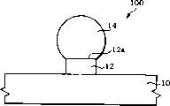
Fig. 1 is an embodiment pattern constructed profile that is suitable for optics 100 of the present invention.Fig. 2 is the pattern schematic plan view of optics 100 shown in Figure 1.In addition, Fig. 1 is the sectional view of the A-A line of presentation graphs 2.
Fig. 3, Fig. 5 and Fig. 7 are respectively the pattern constructed profiles of variation that has changed base component 12 shapes of optics shown in Figure 1 100; Fig. 4, Fig. 6 and Fig. 8 are respectively Fig. 3, Fig. 5 and optics 101,102 shown in Figure 7 and 103 pattern schematic plan view.
Figure 11 is the pattern constructed profile that changes the variation of the base component 12 of optics 100 shown in Figure 1 and optical component 14 shapes; Figure 12 is the pattern schematic plan view of optics 104 shown in Figure 11.
Also have, Figure 27 is the pattern constructed profile that changes the variation of the base component 12 of optics 100 shown in Figure 1 and optical component 14 shapes; Figure 28 is the pattern schematic plan view of optics 105 shown in Figure 27.
The optics 100 of present embodiment comprises: the base component 12 that is provided with on the matrix 10; And the optical component 14 that on the upper surface 12a of base component 12, is provided with.Optical component 14 for example, can have incident light optically focused, polarisation or beam split function, mainly sees figures.1.and.2 below, describes with regard to each textural element of the optics 100 of present embodiment.
(matrix)
As matrix 10, for example, can enumerate the Semiconductor substrate of silicon substrate and GaAs substrate etc. and glass substrate etc.
(base component)
(A) material
In the optics 100 of present embodiment, base component 12 is to be made of the material that can see through specific wavelength light.Specifically, base component 12 is made of the material that can make incident light see through optical component 14.For example, the formation of base component 12 can be adopted polyimide, propylene resin, epoxy resin or polyfurolresin.The base component 12 that present embodiment provides is to be made of the material that can see through specific wavelength light.But base component 12 also can be formed by the material that absorbs specific wavelength light.
In addition, base component 12 can also form one with matrix 10.That is to say that base component 12 and matrix 10 are formed by commaterial.
This base component 12 of picture for example, can form by the mode that forms pattern on matrix 10.
(B) three-dimensional shape
Shown in Fig. 3 to Fig. 8 is the variation (optical component 101,102,103) that changes the three-dimensional shape of base component 12 illustrated in figures 1 and 2.To shown in Figure 8, though the three-dimensional shape of base component is not particularly limited, its structure needs on the surface optical component can be set thereon at least as Fig. 1.For example, as shown in Figure 1, the base component 12 of optical component 100 can be provided with optical component 14 on upper surface 12a.
In addition, as shown in Figure 3 and Figure 4, the upper surface 22a of base component 22 and the angle theta of side 22b can be arranged to acute angle.The side 22b of said here base component 22 is meant the one side that the lateral parts at base component 22 is connected with upper surface 22a.In base component 22, the lateral parts of base component 22 is the side 22b of base component 22.
The formation of optical component 14 is to adopt to shoot out drop to the upper surface 22a of base component 22, and behind the formation optical component predecessor (will set forth below), the method that this optical component predecessor is solidified forms.Therefore, the angle theta that the upper surface 22a of base component 22 and side 22b constitute is an acute angle, therefore, when the upper surface 22a to base component 22 shoots out liquid, can prevent that the side 22b of base component 22 from being soaked by drop.Its result can form the optical component 14 with satisfactory shape and size conscientiously.
In addition, as shown in Figure 5 and Figure 6, the top 32c of the three-dimensional shape of base component 32 can be arranged to the reverse taper shape.In this case, the angle theta of the upper surface 32a of base component 32 and side 32b (one side that is connected with upper surface 32a at the lateral parts of base component 32) also is acute angle.According to this formation, the stability of both sustainable maintenance base component 32 has further been dwindled the angle theta that base component 32 upper surface 32a and side 32b form again.Therefore, the side 32b that can prevent base component 32 is really soaked by drop.Its result can form the optical component 14 with satisfactory shape and size conscientiously.
(C) shape of upper surface
The shape of the upper surface of base component can be determined according to the function and the purposes of the optical component that forms on the upper surface of base component.In other words, by the shape of upper surface of control base component, just can control the shape of optical component.
For example, optics 100 (referring to Fig. 1 and Fig. 2), the shape of the upper surface 12a of its base component 12 is circular.In addition, in the optics 101~103 of Fig. 3~shown in Figure 8, the shape of the upper surface of base component also is circular.
For example, when optical component is used as lens or polarization element, the shape of the upper surface of base component is arranged to circle.Like this, the three-dimensional shape of optical component can form the spherical shape of spherical shape or incision, can use the optical component that is obtained as lens or polarization element.Shown in Fig. 9 is the example that the optical component 14 of optics illustrated in figures 1 and 2 100 is used as lens.That is, as shown in Figure 9, can carry out optically focused with optical component (lens) 14.In addition, be the example that the optical component 14 of optics illustrated in figures 1 and 2 100 is used as polarization element shown in Figure 10.That is, as shown in figure 10, can use optical component (polarization element) 14 to change the direct of travel of light.
In addition, though do not provide diagram here,, when for example optical component was as anisotropy lens or polarization element use, the shape of the upper surface of base component was arranged to ellipse.Therefore, it is spherical that the three-dimensional shape of optical component can form oval ellipse spherical or that cut, resulting optical component can be used as anisotropy lens or polarization element.
Perhaps, for example, when optical component is used as beam splitter (prism), the shape of the upper surface of base component can be arranged to triangle.The formation method of this optical component is: its base component be shaped as triangle, its upper surface is shootd out drop, form the optical component predecessor after, this optical component predecessor solidified and obtain optical component.The described optical component of Xing Chenging can be used as the beam splitter use like this.To set forth in the back about detailed manufacture method.Shown in Figure 11 and Figure 12 is the example that optical component is used as prism.Figure 11 is the sectional view of the A-A line of Fig. 12.As Figure 11 and shown in Figure 12, base component 52 is the triangle column.Therefore, the upper surface 52a's of base component 52 is shaped as triangle.Optical component 24 has beam splitter function (prism).Specifically, as shown in figure 12, the light that incides optical component 24 when outgoing by beam split.
In addition, said base member 12,22,32,42 and 52 any one upper surface all are expressed as and are made of the plane.But shown in Figure 27 and 28, the upper surface 62a of base component 62 also can be a curved surface.In Figure 27 and optical component 105 shown in Figure 28, the optical component 34 that is similar to spherical shape can be arranged on the upper surface 62a of base component 62.
(optical component)
(A) three-dimensional shape
Optical component has the shape that satisfies its purposes and functional requirement.About the three-dimensional shape of optical component, will explanation in the lump in " base component ", so locate to give detailed.
(B) material
About the formation method of optical component 14, for example, curable fluent material is applied heat energy or luminous energy etc., make its sclerosis and form.Specifically, in the present embodiment, be to adopt to shoot out the drop that constitutes by described fluent material to the upper surface 12a of base component 12, behind the formation optical component predecessor (will set forth in the back), this optical component predecessor is hardened form optical component 14.
As described fluent material, for example, can enumerate the predecessor of uv-hardening resin and thermosetting resin.As uv-hardening resin, for example, specifiable acrylic resin and the epoxy resin that UV cured property is arranged.In addition, the example that can provide as thermosetting resin is thermosetting polyimide resin.
2. the manufacture method of optical component
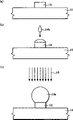
Below, the manufacture method around optical component 100 illustrated in figures 1 and 2 describes with reference to accompanying drawing 13 (a)~Figure 13 (c).Figure 13 (a)~Figure 13 (c) is respectively the pattern constructed profile of a manufacturing process of optical component 100 illustrated in figures 1 and 2.
At first, on matrix 10, form base component 12 (referring to Figure 13 (a)).The formation of base component 12 can be selected suitable method (for example, can select growth method, dry-etching method, wet etching, photosensitive etching method and replica method etc.) according to material and the shape and the size of base component 12.
Then, form optical component 14 (referring to Figure 13 (b)).Specifically, the drop 14b to the upper surface 12a of base component 12 shoots out the fluent material that forms optical component 14 forms the optical component 14a of predecessor.As mentioned above, described fluent material has through 15 character that can harden that energize.
As the spitting method of drop 14b, for example, can enumerate and distribute coating process or ink-jet method.The method of shooing out drop with the distribution coating process is the general method that adopts, and drop 14b is effective for shooing out in a big way.In addition, ink-jet method is to use ink gun to shoot out the method for drop.About shooing out the position of drop, can μ m be that unit controls.The amount of droplets of shooing out can pm be that unit controls, and therefore, can produce the accurate optical component of structure.
And, before drop 14b shoots out, as required, can carry out the hydroscopicity processing by upper surface 12a or carry out the moisture resistance processing base component 12, just can control the wellability of upper surface 12a to drop 14b.Therefore, can form optical component 14 with given shape and size.
Then, make the 14a of optical component predecessor sclerosis, form optical component 14 (referring to Figure 13 (c)).Specifically, give heat energy or luminous energy etc. to the 14a of optical component predecessor.When making the 14a of optical component predecessor sclerosis, adopt suitable method according to described fluent material type.Specifically, for example, specifiable have, and can adopt to give heat energy or with ultraviolet ray or with the light illuminating method of laser etc.By above manufacturing step, just can obtain to comprise the optics 100 (referring to Fig. 1 and Fig. 2) of optical component 14.
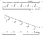
All right, take off optical component 14 from the optics 100 that is obtained, optical component 14 is used as independent optics.For example, as shown in figure 14, the binding site air blowing body 16 (for example inert gas such as argon gas or nitrogen) by to base component 12 and optical component 14 just can take off optical component 14.Perhaps Continuous pressing device for stereo-pattern (not having diagram) on optical component 14 is taken adhesive tape off, just can take off optical component 14 from the upper surface 12a of base component 12.
3. action effect
About the optics of present embodiment with and manufacture method have following action effect.
(1) first, size and shape that can strict control optical component 14.That is to say that the shape of optical component 14 can be controlled according to the jetting amount of drop 14b.The optics of the optical component 14 that like this, just can obtain to comprise that its shape and size all meet the demands.
Be elaborated with reference to accompanying drawing about above-mentioned action effect.Figure 29 is in the manufacturing step (referring to Figure 13 (a)~Figure 13 (c)) of the optics 100 that relates to of described present embodiment, the joint portion of base component 12 and the 14a of optical component predecessor pattern constructed profile nearby, specifically, be the profile of Figure 13 (c).Figure 30 is the pattern constructed profile of the manufacture method of general optics.
At first, before the action effect of describing present embodiment in detail,, describe with reference to accompanying drawing 30 with regard to the manufacture method of general optical component.
(a) manufacture method of general optics
As a kind of manufacture method of optical component, well-known is to shoot out fluent material on matrix 10, behind the formation optical component predecessor, makes this optical component predecessor sclerosis, and obtains the method for optical component.
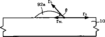
Figure 30 is that fluent material that expression will form optical component is sprayed on the state profile on the matrix 10.Specifically, Figure 30 makes the presclerotic state of described optical component predecessor, promptly is that expression will be arranged on the state on the matrix 10 by the 92a of optical component predecessor that fluent material constitutes.
In Figure 30, if establish γ
sFor the surface tension of matrix 10, establish γ
LFor fluent material (optical component predecessor's) surface tension, establish γ
SLFor the interfacial tension of matrix 10 and fluent material, to establish fluent material be θ, then γ for the contact angle of matrix 10
S, γ
L, γ
SL, between relation, available following formulate:
γ
s=γ
sL+2
Lcos?θ……….(1)
The curvature of the 92a of optical component predecessor that is formed by fluent material has been subjected to the restriction of the contact angle θ of formula (1).That is to say that after the 92a of the optical component predecessor sclerosis, the curvature of the optical component of acquisition depends primarily on the material of matrix 10 and described fluent material.The curvature of optical component is a key factor of decision optical component shape.Therefore, this manufacture method is difficult to the formed optical component shape of control.
And in this case, though diagram not here at matrix 10 lip-deep ad-hoc locations, forms after the film of adjusting wetting angle, again by shooing out the drop of fluent material, the method that makes the contact angle θ of fluent material increase is that people are known.Utilize this method, can control the shape of optical component to a certain extent.But, wanting by forming the film of this adjustment wetting angle, the shape of control optical component is limited.
(b) manufacture method of the optics of present embodiment.
At above-mentioned shortcoming, the manufacture method of the optics of present embodiment, as shown in figure 29, the 14a of predecessor of optical component can form on the upper surface 12a of base component 12.Therefore, the side 12b of base component 12 only otherwise because of the 14a of optical component predecessor soaks, the surface tension of base component 12 just can not act on the 14a of optical component predecessor, mainly is the surface tension γ of the 14a of optical component predecessor
LWork.Therefore, form the used amount of droplets of the optical component 14a of predecessor, just can control the shape of the 14a of optical component predecessor by adjusting.And then, the optical component 14 that just can obtain to have satisfied shape and size.
(2) second, can strict control optical component 14 the position is set.
As mentioned above, optical component 14 is to shoot out drop 14b by the upper surface 12a to base component 12, behind the formation optical component 14a of predecessor, makes the 14a of optical component predecessor sclerosis again and (referring to Figure 13 (b)) of formation.Generalized case, the drop point site of the drop that shoots out are difficult to strict control.But, according to this method, then need not carry out the position adjustment especially, just can on the upper surface 12a of base component 12, form optical component 14.That is, only on the upper surface 12a of base component 12, shoot out drop 14b, need not carry out the position adjustment and just can form the 14a of optical component predecessor.In other words, the bearing accuracy during with formation base component 12 just can form optical component 14.Therefore, be easy to obtain to be provided with the optical component 14 that the position is controlled.
(3) the 3rd, the shape of the upper surface 12a by setting base component 12 just can be set the shape of optical component 14.That is, the shape of the upper surface 12a by suitable selection base component 12 just can form the optical component 14 with specific function.Therefore, the shape of the upper surface 12a by changing base component 12 can also be provided with a plurality of optical components with difference in functionality on same matrix.
(4) the 4th, by the height of control base component 12, the just distance of may command matrix 10 and optical component 14.Therefore, be easy to adjust the position of matrix 10 and optical component 14, adopt easy method, just can form the optical component 14 that the position is controlled is set.
The present invention is not limited only to above-mentioned embodiment, can carry out various distortion.For example, the present invention includes with present embodiment in the identical in fact formation of the formation that illustrates (for example, function, method and the formation that comes to the same thing, perhaps purpose and the formation that comes to the same thing).In addition, the present invention also comprises the part that can replace the non-intrinsically safe formation of setting forth in embodiment.The present invention also comprise with present embodiment in the formation that illustrates have the formation of same purpose effect or can reach the formation of same purpose.And the present invention also is included in the formation of additional known technology in the formation of present embodiment explanation.
Embodiment
Below, describe with regard to the embodiment that adopts above-mentioned embodiment.What any one of embodiment 1~3 provided all is the example that the optical component 100 of present embodiment is used for the lenticule substrate.For example, the lenticule substrate can be arranged on the pixel parts of liquid crystal display face version, the sensitive surface of solid camera head (CCD) and the optical coupling part of optical fiber.In addition, embodiment 4 is methods that the optical component 14 that is obtained at embodiment 1 is taken off in expression.
(embodiment 1)
1. the structure of lenticule substrate
Figure 15 is the pattern constructed profile of the lenticule substrate 200 that relates to of expression embodiment 1.Figure 16 is the pattern schematic plan view of the lenticule substrate 200 shown in Fig. 15.In addition, Figure 15 is the mode chart of the section cut open along Figure 16 A-A line.
As shown in figure 15, lenticule substrate 200 can be provided with a plurality of optical components 114.Optical component 114 is arranged on the top 112a of base component 112.Base component 112 is arranged on the matrix 110.
In the present embodiment, be illustrated around following formation situation: matrix 110 is to be made of glass substrate; Base component 112 is to be made of polyimide resin; And optical component 114 is to be made of uv-hardening resin.
In addition, for fixing optical member 114, in case of necessity, can be at the packing matcrial 160 (referring to Figure 26) on every side of optical component 114.And, with the embodiment 2 that sets forth in the back and embodiment 3 too, as required, also can be around optical component 114 packing matcrial 160.Encapsulant 160 preferably adopts than the little material of material refractive index that constitutes optical component 114.Encapsulant 160 is not particularly limited, and for example can use resin material.
2. the manufacture method of lenticule substrate
Below, describe with regard to the manufacture method of the lenticule substrate 200 of present embodiment.Figure 17 (a)~Fig. 17 (e) and Figure 18 (a) and Figure 18 (b) are respectively the pattern constructed profiles of a manufacturing process of Figure 15 and lenticule substrate 200 shown in Figure 16.
At first, on the matrix 110 that forms by glass substrate, after the coating polyimide predecessor, under 150 ℃ temperature, heat-treating (referring to Figure 17 (a)) greatly.Thus, form resin bed 112x.This resin bed 112x is the state that can keep shape, and is again the state that does not harden fully.
Then, after forming protective seam R1 on the resin bed 112x, use mask 130, carry out lithography step (referring to Figure 17 (b)) with specific pattern.With this, form the protective seam R1 (referring to Figure 17 (c)) of specific pattern.
Then, protective seam R1 as mask, for example, is carried out Wet-type etching by using alkaline solution, make resin bed 112x form pattern (referring to Figure 17 (d)).Then, remove protective seam R1, under about 350 ℃ temperature, heat-treat, thereby make base component 112 harden fully (referring to Figure 17 (e)).
Then, 112a above base component 112 shoots out fluent material drop 114b with ink gun 117, forms the 114a of optical component predecessor (lens predecessor).This optical component 114a of predecessor passes through cure step afterwards, can change into optical component 114 (referring to Figure 15 and Figure 16).In addition, in the present embodiment, around the predecessor who adopts uv-hardening resin as described fluent material, the situation that adopts ink ejecting method to shoot out drop 114b describes.As required, through repeatedly shooing out drop 114b, can on base component 112, form the 114a of optical component predecessor on the 112a with satisfactory shape and size.
Follow, the irradiation to the 114a of optical component predecessor carries out ultraviolet ray 115 forms optical component 114 (referring to Figure 18 (b)) again.According to shape and size and the material of optical component 114a, suitably adjust the ultraviolet irradiation amount.Can form optical component (lens) 114 by above step.Like this, can obtain comprising the lenticule substrate 200 (referring to Figure 15 and Figure 16) of optical component 114.
According to the lenticule substrate 200 and the manufacture method thereof of present embodiment, has same action effect with the optics and the manufacture method thereof of present embodiment.
(embodiment 2)
1. the structure of lenticule substrate
Figure 19 is the pattern constructed profile of the lenticule substrate 300 that relates to of embodiment 2.Figure 20 is the pattern schematic plan view of lenticule substrate 300 shown in Figure 19.In addition, Figure 19 is the section pattern diagram of cutting open along the A-A line of Figure 20.
The lenticule substrate 300 that present embodiment relates to has on the brim of a hat shape this point at base component 132, has different structures with the lenticule substrate 200 of embodiment 1.All the lenticule substrate 200 with embodiment 1 is the same but other constitute, and therefore, the explanation of structure same place is omitted.
The base component 112 of base component 132 and embodiment 1 is the same, is formed by polyimide resin, and as Figure 19 and shown in Figure 20, base component 132 has the brim of a hat shape.In other words, the top 132c of base component 132 forms the reverse taper shape.In this case, the angle theta that forms of the upper surface 132a of base component 132 and side 132b (face that is connected with upper surface 132a at the lateral parts of base component 132) is an acute angle.According to this formation, can further dwindle the upper surface 132a of base component 132 and the angle theta that side 132b forms.Therefore, can prevent really that the side 132b of base component 132 from being soaked by drop, thereby form the optical component 14 of satisfactory shape and size more accurately.
2. the manufacture method of lenticule substrate
Below, the manufacture method of the lenticule substrate 300 that relates to regard to present embodiment describes.Figure 21 (a) is respectively the pattern constructed profile of a manufacturing step of Figure 19 and lenticule substrate 300 shown in Figure 20 to Figure 21 (e).
The manufacture method of the lenticule substrate 300 of present embodiment, except the pattern of base component 132 formed step, all the manufacture method with the lenticule substrate 200 of embodiment 1 was identical for other.Therefore, the pattern formation step of base component 132 mainly is described here.
At first, after forming resin bed 112x on the substrate 10 that forms by glass substrate, form the protective seam R1 (referring to Figure 21 (a) to Figure 21 (c)) of specific pattern again.The step before this all manufacture method with embodiment 1 is identical.
Then, under the temperature that can not make protective seam generation qualitative change (for example 130 ℃), heat-treat.When thermal treatment, preferably the upper surface from resin bed 112x heats downwards, and the hardenability of upper surface (protective seam R1 side) that makes resin bed 112x is greater than 110 parts of the substrate among the resin bed 112x.
Then, protective seam R1 as mask, is carried out Wet-type etching to resin bed 112x.In this operation, part under the protective seam R1, promptly the top of resin bed 112x is slow because of the permeating speed of etching solution, therefore, is difficult to etching than other parts.In addition, by described thermal treatment, the hardenability of the upper surface portion of resin bed 112x is greater than the hardenability of substrate 110 parts.Therefore, the upper surface portion of resin bed 112x, the rate of etch in etching are also less than substrate 110 parts.Therefore, when this Wet-type etching, the upper surface of resin bed 112x is slow than the etching speed of substrate 110 parts, so, residual more of upper surface part proportion by subtraction substrate 110 parts of resin bed 112x.Thereby can obtain top 132c is the pedestal 132 (referring to Figure 21 (d)) of reverse taper shape.Then, remove protective seam R1 (referring to Figure 21 (e)).
After this operation is identical with the manufacture method of embodiment 1.Therefore, can obtain lenticule substrate 300 (referring to Figure 19 and Figure 20).
According to the lenticule substrate 300 and the manufacture method thereof of present embodiment, have optics and the same action effect of manufacture method thereof with present embodiment.
(embodiment 3)
1. the structure of lenticule substrate
Figure 22 is the pattern constructed profile that embodiment 1 relates to lenticule substrate 400.Figure 23 is the pattern schematic plan view of lenticule substrate 400 shown in Figure 22.In addition, Figure 22 is the section pattern diagram of cutting open along the A-A line of Figure 23.
As shown in figure 22, in the lenticule substrate 400 of present embodiment, base component 152 and matrix 110 forms an integral body, and be different by the formation of material (glass substrate) formation this point the same with matrix 110 and embodiment 1.But other formations are the same with the lenticule substrate 200 of embodiment 1, and therefore, the explanation of structure same place is omitted.
2. the manufacture method of lenticule substrate
Below, describe with regard to the manufacture method of present embodiment lenticule substrate 400.Figure 24 (a) is respectively the pattern constructed profile of a manufacturing process of Figure 22 and lenticule substrate 400 shown in Figure 23 to Figure 24 (e).
At first, on the substrate 110 that is formed by glass substrate, lamination forms dry type film diaphragm, (referring to Figure 24 (a)).
Then, use the mask 230 of specific pattern to carry out photosensitive etching step (referring to Figure 24 (b)), thereby form the protective seam R2 (referring to Figure 24 (c)) of specific pattern.
Then, be mask with protective seam R2, make the matrix 110 that constitutes by glass substrate form pattern (referring to Figure 24 (d)).By this pattern, make base component 152 and matrix 110 form one.Be to separate with otch between the base component 152 of adjacency.
Have as the method for pattern formation is specifiable: methods such as fluoric acid Wet-type etching, ion beam milling, laser accurate processing and sandblast.Wherein, when pattern formation area is bigger, adopt blasting method effective.Blasting method is to be that the particulate of 1 μ m to tens μ m carries out etching method to processed goods sprayed particle diameter, can obtain the resolution of 20 μ m degree.The particulate that can be used for blasting method for example has SiC and AIO
2Deng.Then, remove protective seam R2 (referring to Figure 24 (e)).
After this manufacturing process is identical with the manufacture method of embodiment 1.Therefore can obtain lenticule substrate 400 (referring to Figure 22 and Figure 23).
According to the lenticule substrate 400 and the manufacture method thereof of present embodiment, have the optics and the same action effect of its manufacture method that relate to present embodiment.
(embodiment 4)
1. the method for taking off of optical component 114
In embodiment 4, the method that the lenticule substrate 200 how main elaboration obtains from embodiment 1 takes off optical component 14.Figure 25 (a) and Figure 25 (b) are respectively the pattern constructed profiles that the method for the optical component 114 that present embodiment relates to is taken off in expression.Be removed the optical component 114 that comes can be separately as the parts use of other equipment.Specifically, optical component 114 is as the globe lens parts, and the parts that can be used as other devices use.
At first, on the optical component 114 of the lenticule substrate 200 of embodiment 1, adhesive sheet 150 (referring to Figure 25 (a)) is set.Then, by taking adhesive sheet 150 off, optical component 114 is taken off (referring to Figure 25 (b)) from base component 112 again.Adopt above step just can take off optical component 114.At this moment, if in advance the upper surface 112a execution moisture-resistant of base component 112 is handled, then be easy to take off.
In addition, what provide in the present embodiment is the method for taking off optical component 114 from the lenticule substrate 200 of embodiment 1, but adopt the method for present embodiment, also can take off optical component 114 from the lenticule substrate 300,400 of embodiment 2 or embodiment 3.
Also have, in the present embodiment, introduction be the method for taking off optical component from the lenticule substrate with lens function, but when taking off optical component, also can adopt the method identical with present embodiment with non-lens function from optics.
The above is the preferred embodiments of the present invention only, is not limited to the present invention, and for a person skilled in the art, the present invention can have various changes and variation.Within the spirit and principles in the present invention all, any modification of being done, be equal to replacement, improvement etc., all should be included within the claim scope of the present invention.
Description of reference numerals
10,110 matrixes;
12,22,32,42,52,62,112,132,152 base components;
12a, 22a, 32a, 42a, 52a, 62a, 112a, 132a, 152a base component Upper surface;
12b, 22b, the side of 32b base component;
The upper part of 32c base component;
14,24,34,114 optical components;
14a optical component predecessor;
The 14b drop;
15 energy;
16 gases;
17 drops shoot out mouth;
100,101,102,103,104,105 opticses;
The 112x resin bed;
114a optical component predecessor;
The 114b drop;
115 ultraviolet rays;
117 ink guns;
130,230 masks;
150 adhesive sheets;
160 encapsulants;
200,210,300,400 lenticule substrates;
R1, the R2 protective layer
Claims (36)
1. an optics comprises: be arranged on the base component on the matrix; And the optical component that is arranged at the upper surface of described base component.
2. optics according to claim 1, wherein, described base component is formed by the material that can see through specific wavelength light.
3. optics according to claim 1, wherein, described optical component has lens function.
4. optics according to claim 1, wherein, described optical component has the polarization element function.
5. optics according to claim 1, wherein, described optical component has the beam splitter function.
6. optics according to claim 1, wherein, described optical component is a spherical shape or oval spherical.
7. optics according to claim 1, wherein, described optical component is the oval spherical of the spherical shape of part excision or part excision.
8. optics according to claim 1, wherein,
The upper surface of described base component is a triangle;
Described optical component is to shoot out drop by the upper surface to described base component, forms after the optical component predecessor, and this optical component predecessor is solidified to form.
9. optics according to claim 1, wherein, the cross section of described optical component is a circle or oval.
10. according to each described optics in the claim 1 to 9, wherein, described optical component is by applying energy curable fluent material to be solidified to form.
11. optics according to claim 10, wherein, described optical component is formed by ultraviolet curing resin.
12. optics according to claim 10, wherein, described optical component is formed by the thermohardening type resin.
13. optics according to claim 1, wherein, the upper surface of described base component is any one shape in circle, ellipse or the triangle.
14. optics according to claim 1, wherein, the upper surface of described base component is a curved surface.
15. optics according to claim 1, wherein, the formed angle of the face that is connected to this upper surface in the upper surface of described base component and the lateral parts of described base component is an acute angle.
16. optics according to claim 1, wherein, the top of described base component is the reverse taper shape.
17. optics according to claim 1, wherein, described base component and described matrix form an integral body.
18. optics according to claim 1, wherein, described optical component is a lenticule, has the function of lenticule substrate.
19. optics according to claim 1 wherein, has been filled encapsulant around the described optical component.
20. the manufacture method of an optics may further comprise the steps:
(a) on matrix, form base component;
(b) upper surface to described base component shoots out drop, forms the optical component predecessor;
(c) described optical component predecessor is solidified, form optical component.
21. the manufacture method of optics according to claim 20, wherein, in described step (a), described base component adopts the material of the light that can see through specific wavelength to form.
22., wherein, in described step (b), adopt ink-jet method to carry out shooing out of described drop according to the manufacture method of claim 20 or 21 described opticses.
23. according to the manufacture method of each described optics in the claim 20 to 22, wherein, in described step (c), described optical component predecessor's curing is to adopt the method that applies energy to carry out.
24. manufacture method according to each described optics in the claim 20 to 23, wherein, (a) forms described base component in described step, so that the angle that the face that is connected to this upper surface in the side of the upper surface of described base component and described base component constitutes is an acute angle.
25. according to the manufacture method of each described optics in the claim 20 to 24, wherein, in described step (a), the reverse taper shape is formed at the top of described base component.
26., in described step (b) before, also comprise according to the manufacture method of each described optics in the claim 20 to 25: step (d), adjust the wellability of the upper surface of described base component with respect to described drop.
27. according to the manufacture method of each described optics in the claim 20 to 26, wherein, described optical component is a lenticule, described optics is the lenticule substrate.
28. the manufacture method according to each described optics in the claim 20 to 27 also comprises: step (e), to filling with encapsulant around the described optical component.
29. the manufacture method of an optics may further comprise the steps:
(a) on matrix, form base component;
(b) upper surface to described base component shoots out drop, forms the optical component predecessor;
(c) described optical component predecessor is solidified, form optics;
(d) above described base component, take off described optical component.
30. the manufacture method of optics according to claim 29, wherein, at described step (a), employing can see through the material of the light of specific wavelength, forms described base component.
31. a lenticule substrate comprises: base component that on substrate, is provided with and the lens that are provided with at the upper surface of described base component.
32. lenticule substrate according to claim 31, wherein, described base component is to be formed by the material that can see through the light of specific wavelength.
33. the manufacture method of a lenticule substrate comprises:
(a) on matrix, form base component;
(b) upper surface to described base component shoots out drop, forms the lens predecessor;
(c) described lens predecessor is solidified, form lens.
34. the manufacture method of lenticule substrate according to claim 33, wherein, in described step (a), the material that employing can see through the light of specific wavelength forms described base component.
35. a display device has according to claim 31 or 32 described lenticule substrates.
36. an imaging apparatus has according to claim 31 or 32 described lenticule substrates.
Applications Claiming Priority (2)
| Application Number | Priority Date | Filing Date | Title |
|---|---|---|---|
| JP2002279064A JP3719431B2 (en) | 2002-09-25 | 2002-09-25 | OPTICAL COMPONENT, ITS MANUFACTURING METHOD, DISPLAY DEVICE, AND IMAGING ELEMENT |
| JP2002279064 | 2002-09-25 |
Publications (1)
| Publication Number | Publication Date |
|---|---|
| CN1490635A true CN1490635A (en) | 2004-04-21 |
Family
ID=32040444
Family Applications (1)
| Application Number | Title | Priority Date | Filing Date |
|---|---|---|---|
| CNA031569722A Pending CN1490635A (en) | 2002-09-25 | 2003-09-16 | Optical component and producing method thereof, lenticule substrate and producing method thereof, displaying device, camera component |
Country Status (6)
| Country | Link |
|---|---|
| US (1) | US7179728B2 (en) |
| EP (2) | EP1582892B1 (en) |
| JP (1) | JP3719431B2 (en) |
| KR (1) | KR100739085B1 (en) |
| CN (1) | CN1490635A (en) |
| DE (2) | DE60318905T2 (en) |
Cited By (6)
| Publication number | Priority date | Publication date | Assignee | Title |
|---|---|---|---|---|
| US7259915B2 (en) | 2004-05-31 | 2007-08-21 | Lg Electronics Inc. | Microlens array sheet |
| CN102928899A (en) * | 2011-08-08 | 2013-02-13 | 索尼公司 | Diffusion sheet, backlight, liquid crystal display apparatus, and method of producing a diffusion sheet |
| CN105116612A (en) * | 2015-09-22 | 2015-12-02 | 京东方科技集团股份有限公司 | Optical diaphragm, backlight module and display device |
| CN106526722A (en) * | 2016-11-09 | 2017-03-22 | 中南大学 | Method for controlling shape of mini liquid drop |
| US9804367B2 (en) | 2015-11-04 | 2017-10-31 | Omnivision Technologies, Inc. | Wafer-level hybrid compound lens and method for fabricating same |
| CN110519943A (en) * | 2018-05-21 | 2019-11-29 | Unijet株式会社 | Multi-layer board manufacturing method |
Families Citing this family (24)
| Publication number | Priority date | Publication date | Assignee | Title |
|---|---|---|---|---|
| JP4088779B2 (en) | 2003-04-25 | 2008-05-21 | セイコーエプソン株式会社 | Coupling structure and coupling method between optical fibers |
| JP4155099B2 (en) * | 2003-05-16 | 2008-09-24 | セイコーエプソン株式会社 | Microlens manufacturing method |
| JP3800199B2 (en) * | 2003-05-16 | 2006-07-26 | セイコーエプソン株式会社 | Microlens manufacturing method |
| JP4120813B2 (en) | 2003-06-12 | 2008-07-16 | セイコーエプソン株式会社 | Optical component and manufacturing method thereof |
| JP3719441B2 (en) | 2003-08-01 | 2005-11-24 | セイコーエプソン株式会社 | Optical element and method for manufacturing the same, optical module, and optical transmission device |
| JP4241259B2 (en) * | 2003-08-06 | 2009-03-18 | セイコーエプソン株式会社 | Microlens manufacturing method |
| DE102004030418A1 (en) * | 2004-06-24 | 2006-01-19 | Robert Bosch Gmbh | Microstructured infrared sensor and a method for its production |
| JP2006030634A (en) * | 2004-07-16 | 2006-02-02 | Seiko Epson Corp | Method for manufacturing microlens |
| KR100636349B1 (en) | 2004-09-24 | 2006-10-19 | 엘지전자 주식회사 | Microlens Array Sheet and Manufacturing Method thereof |
| JP2006323147A (en) * | 2005-05-19 | 2006-11-30 | Seiko Epson Corp | Manufacturing method of microlens, microlens, optical film, screen for projection, projector system, electrooptical apparatus, and electronic equipment |
| JP2006350177A (en) * | 2005-06-20 | 2006-12-28 | Seiko Epson Corp | Manufacturing method of optical sheet, optical sheet, planar lighting device, and electrooptical apparatus |
| JP2007010707A (en) * | 2005-06-28 | 2007-01-18 | Seiko Epson Corp | Method for manufacturing optical sheet, optical sheet, backlight unit, display device, and electronic apparatus |
| JP2007036140A (en) * | 2005-07-29 | 2007-02-08 | Seiko Epson Corp | Photoelement and its manufacturing method |
| JP2007080884A (en) * | 2005-09-09 | 2007-03-29 | Asahi Glass Co Ltd | Light emitting device, method of manufacturing the same, and intermediate part therefor |
| KR100774218B1 (en) * | 2006-09-28 | 2007-11-08 | 엘지전자 주식회사 | Lens, a method for manufacturing it and light emitting device package |
| US8115920B2 (en) * | 2007-11-14 | 2012-02-14 | 3M Innovative Properties Company | Method of making microarrays |
| JP2010223975A (en) * | 2009-03-19 | 2010-10-07 | Dhs:Kk | Method of manufacturing lens array and lens array |
| JP2011076800A (en) * | 2009-09-29 | 2011-04-14 | Fujifilm Corp | Organic el element, and manufacturing method thereof |
| SG194130A1 (en) | 2011-04-12 | 2013-11-29 | Pixeloptics Inc | Adhesive dispensing profile enhancement |
| TW201316383A (en) * | 2011-10-12 | 2013-04-16 | Univ Nat Taiwan | Method for producing silicon waveguides on non-SOI substrate |
| US8828484B2 (en) * | 2013-01-28 | 2014-09-09 | Taiwan Semiconductor Manufacturing Co., Ltd. | Self-alignment due to wettability difference of an interface |
| US20160327747A1 (en) * | 2013-11-08 | 2016-11-10 | Empire Technology Development Llc | Printed ball lens and methods for their fabrication |
| KR102095003B1 (en) | 2017-01-03 | 2020-03-30 | 주식회사 엘지화학 | Method for preparing resin particle |
| DE102017003721A1 (en) * | 2017-03-01 | 2018-09-06 | Docter Optics Se | Method of manufacturing a micro projector for a projection display |
Family Cites Families (34)
| Publication number | Priority date | Publication date | Assignee | Title |
|---|---|---|---|---|
| US4689291A (en) | 1985-08-30 | 1987-08-25 | Xerox Corporation | Pedestal-type microlens fabrication process |
| JPS6283337A (en) | 1985-10-04 | 1987-04-16 | Hoya Corp | Production of microlens array |
| JPH02165932A (en) | 1988-12-20 | 1990-06-26 | Seiko Epson Corp | Manufacture of microlens array |
| US5229016A (en) | 1991-08-08 | 1993-07-20 | Microfab Technologies, Inc. | Method and apparatus for dispensing spherical-shaped quantities of liquid solder |
| JP3198003B2 (en) | 1993-12-24 | 2001-08-13 | 学校法人桐蔭学園 | Light fast fibroin-natural dye complex |
| US5498444A (en) | 1994-02-28 | 1996-03-12 | Microfab Technologies, Inc. | Method for producing micro-optical components |
| JPH0882759A (en) | 1994-09-09 | 1996-03-26 | Canon Inc | Optical scanner |
| JP3241251B2 (en) * | 1994-12-16 | 2001-12-25 | キヤノン株式会社 | Method of manufacturing electron-emitting device and method of manufacturing electron source substrate |
| US5846694A (en) | 1996-02-13 | 1998-12-08 | The Regents Of The University Of California | Microminiature optical waveguide structure and method for fabrication |
| JP3764199B2 (en) | 1996-03-05 | 2006-04-05 | 株式会社リコー | Light source device |
| GB9611582D0 (en) * | 1996-06-04 | 1996-08-07 | Thin Film Technology Consultan | 3D printing and forming of structures |
| EP1365443A3 (en) | 1996-09-19 | 2004-11-17 | Seiko Epson Corporation | Matrix type display device and manufacturing method thereof |
| DE19712297A1 (en) | 1997-03-24 | 1998-10-01 | Bosch Gmbh Robert | Process for the production of light-guiding structures |
| EP1376229B1 (en) | 1997-08-08 | 2010-10-13 | Dai Nippon Printing Co., Ltd. | Plate for lithography and process for producing the same |
| JP3920461B2 (en) | 1998-06-15 | 2007-05-30 | 大日本印刷株式会社 | Lens and manufacturing method thereof |
| DE69840914D1 (en) * | 1997-10-14 | 2009-07-30 | Patterning Technologies Ltd | Method for producing an electrical capacitor |
| JP4217294B2 (en) | 1998-04-28 | 2009-01-28 | Hoya株式会社 | Optical element bonding device |
| US6074888A (en) | 1998-08-18 | 2000-06-13 | Trw Inc. | Method for fabricating semiconductor micro epi-optical components |
| JP2000108216A (en) | 1998-10-02 | 2000-04-18 | Canon Inc | Manufacture of microlens array |
| JP4275233B2 (en) | 1999-01-06 | 2009-06-10 | 大日本印刷株式会社 | Optical element and manufacturing method thereof |
| JP2000280367A (en) | 1999-03-30 | 2000-10-10 | Seiko Epson Corp | Apparatus and method for manufacturing microlens |
| JP2001208958A (en) | 2000-01-26 | 2001-08-03 | Fuji Photo Film Co Ltd | Optical device |
| US20010048968A1 (en) | 2000-02-16 | 2001-12-06 | Cox W. Royall | Ink-jet printing of gradient-index microlenses |
| US6625351B2 (en) | 2000-02-17 | 2003-09-23 | Microfab Technologies, Inc. | Ink-jet printing of collimating microlenses onto optical fibers |
| TW463058B (en) | 2000-10-20 | 2001-11-11 | Ind Tech Res Inst | Method for fabricating microlens in batch and product manufactured the same |
| JP3899879B2 (en) | 2000-11-21 | 2007-03-28 | セイコーエプソン株式会社 | Color filter manufacturing method and manufacturing apparatus, liquid crystal device manufacturing method and manufacturing apparatus, EL device manufacturing method and manufacturing apparatus, inkjet head control apparatus, material discharging method and material discharging apparatus, and electronic apparatus |
| JP3491155B2 (en) | 2000-11-21 | 2004-01-26 | セイコーエプソン株式会社 | Material discharging method and apparatus, color filter manufacturing method and manufacturing apparatus, liquid crystal device manufacturing method and manufacturing apparatus, EL device manufacturing method and manufacturing apparatus |
| JP2002169004A (en) | 2000-11-29 | 2002-06-14 | Ind Technol Res Inst | Batch-produced microlens array and method for producing the same |
| JP2002202426A (en) | 2000-12-28 | 2002-07-19 | Matsushita Electric Ind Co Ltd | Method for manufacturing optical waveguide |
| CN1193249C (en) | 2001-02-12 | 2005-03-16 | 财团法人工业技术研究院 | Optical fibre aligning element for integrated microspheric lens |
| GB2373095A (en) * | 2001-03-09 | 2002-09-11 | Seiko Epson Corp | Patterning substrates with evaporation residues |
| JP3998921B2 (en) | 2001-05-11 | 2007-10-31 | 日本電信電話株式会社 | Microlens formation method |
| JP4141674B2 (en) | 2001-10-22 | 2008-08-27 | セイコーエプソン株式会社 | Droplet discharge head, wiping method thereof, and electronic apparatus equipped with the same |
| JP4161590B2 (en) | 2002-02-22 | 2008-10-08 | セイコーエプソン株式会社 | Microlens manufacturing method, microlens, optical film, projection screen, and projector system |
-
2002
- 2002-09-25 JP JP2002279064A patent/JP3719431B2/en not_active Expired - Fee Related
-
2003
- 2003-08-28 US US10/649,891 patent/US7179728B2/en not_active Expired - Fee Related
- 2003-09-04 EP EP05011306A patent/EP1582892B1/en not_active Expired - Lifetime
- 2003-09-04 EP EP03019615A patent/EP1411376B1/en not_active Expired - Lifetime
- 2003-09-04 DE DE60318905T patent/DE60318905T2/en not_active Expired - Lifetime
- 2003-09-04 DE DE60302526T patent/DE60302526T2/en not_active Expired - Lifetime
- 2003-09-16 CN CNA031569722A patent/CN1490635A/en active Pending
- 2003-09-24 KR KR1020030066127A patent/KR100739085B1/en not_active IP Right Cessation
Cited By (9)
| Publication number | Priority date | Publication date | Assignee | Title |
|---|---|---|---|---|
| US7259915B2 (en) | 2004-05-31 | 2007-08-21 | Lg Electronics Inc. | Microlens array sheet |
| CN102928899A (en) * | 2011-08-08 | 2013-02-13 | 索尼公司 | Diffusion sheet, backlight, liquid crystal display apparatus, and method of producing a diffusion sheet |
| CN105116612A (en) * | 2015-09-22 | 2015-12-02 | 京东方科技集团股份有限公司 | Optical diaphragm, backlight module and display device |
| US9804367B2 (en) | 2015-11-04 | 2017-10-31 | Omnivision Technologies, Inc. | Wafer-level hybrid compound lens and method for fabricating same |
| TWI610099B (en) * | 2015-11-04 | 2018-01-01 | 豪威科技股份有限公司 | Wafer-level hybrid compound lens and method for fabricating same |
| CN106526722A (en) * | 2016-11-09 | 2017-03-22 | 中南大学 | Method for controlling shape of mini liquid drop |
| CN106526722B (en) * | 2016-11-09 | 2018-04-24 | 中南大学 | A kind of method for controlling miniature droplets shape |
| CN110519943A (en) * | 2018-05-21 | 2019-11-29 | Unijet株式会社 | Multi-layer board manufacturing method |
| CN110519943B (en) * | 2018-05-21 | 2022-07-26 | Unijet株式会社 | Method for manufacturing multilayer board |
Also Published As
| Publication number | Publication date |
|---|---|
| DE60302526T2 (en) | 2006-08-10 |
| KR20040027369A (en) | 2004-04-01 |
| EP1411376B1 (en) | 2005-11-30 |
| EP1411376A1 (en) | 2004-04-21 |
| EP1582892A1 (en) | 2005-10-05 |
| JP3719431B2 (en) | 2005-11-24 |
| JP2004117660A (en) | 2004-04-15 |
| KR100739085B1 (en) | 2007-07-13 |
| DE60318905D1 (en) | 2008-03-13 |
| US20040106223A1 (en) | 2004-06-03 |
| DE60302526D1 (en) | 2006-01-05 |
| EP1582892B1 (en) | 2008-01-23 |
| US7179728B2 (en) | 2007-02-20 |
| DE60318905T2 (en) | 2009-01-29 |
Similar Documents
| Publication | Publication Date | Title |
|---|---|---|
| CN1490635A (en) | Optical component and producing method thereof, lenticule substrate and producing method thereof, displaying device, camera component | |
| CN100351032C (en) | Laser based splitting method, object to be split, and semiconductor element chip | |
| CN1229653C (en) | Lenticular array making method, liquid crystal display device and making method and projector | |
| CN1268942C (en) | Substrate and method of manufacturing the same, microlens substrate, transmission screen and rear projector | |
| CN1295521C (en) | Micro lens and making method thereof, optical device, optical transmitting device and head for laser printer | |
| CN1573363A (en) | Optical part and its manufacturing method | |
| CN1320374C (en) | Lens array unit method of producing lens array unit and optical device using lens array unit | |
| CN1993634A (en) | Condensing element, solid-state imaging device and method for fabricating the same | |
| CN1862292A (en) | Method of manufacturing a microlens substrate, and its application | |
| CN1219223C (en) | Resin-bond type optical element, production method therefor and optical article | |
| CN101043992A (en) | Brittle material scribing method and scribing apparatus | |
| CN1294426C (en) | Lens substrate, method of manufacturing the same, transmission screen, and rear projector | |
| CN1501696A (en) | Image pickup device and portable terminal equipped therewith | |
| CN1377181A (en) | Image pick-up module and device | |
| CN1428618A (en) | Optical enclosed chip, optical device, optical module and method for moulded optical enclosed chip | |
| CN1894606A (en) | Collective element and solid-state imaging device | |
| CN1383215A (en) | Semiconductor device and its mfg. method | |
| CN1579022A (en) | Solid-state imaging device and manufacturing method therefor | |
| CN1450377A (en) | Projective lens, method for making projective lens and projector installed with projective lens | |
| CN1928711A (en) | Mold, imprint method, and process for producing chip | |
| CN1924618A (en) | Microlens substrate, a liquid crystal panel and a projection type display apparatus | |
| CN1595285A (en) | Screen member for a transmissive screen, transmissive screen and rear projection | |
| CN1790158A (en) | Lens substrate, method for manufacturing lens substrate, transmission screen and rear projection device | |
| CN1821837A (en) | Liquid crystal display device and production method thereof, and projector | |
| CN1573582A (en) | Microlens base materials, method for forming coloring layer, transmission screen and rear projection |
Legal Events
| Date | Code | Title | Description |
|---|---|---|---|
| C06 | Publication | ||
| PB01 | Publication | ||
| C10 | Entry into substantive examination | ||
| SE01 | Entry into force of request for substantive examination | ||
| C02 | Deemed withdrawal of patent application after publication (patent law 2001) | ||
| WD01 | Invention patent application deemed withdrawn after publication |