CN1484302A - High radiation miniature package for semiconductor chip - Google Patents
High radiation miniature package for semiconductor chip Download PDFInfo
- Publication number
- CN1484302A CN1484302A CNA021431965A CN02143196A CN1484302A CN 1484302 A CN1484302 A CN 1484302A CN A021431965 A CNA021431965 A CN A021431965A CN 02143196 A CN02143196 A CN 02143196A CN 1484302 A CN1484302 A CN 1484302A
- Authority
- CN
- China
- Prior art keywords
- chip
- lead frame
- substrate
- frame
- foot pad
- Prior art date
- Legal status (The legal status is an assumption and is not a legal conclusion. Google has not performed a legal analysis and makes no representation as to the accuracy of the status listed.)
- Pending
Links
Images


Classifications
-
- H—ELECTRICITY
- H01—ELECTRIC ELEMENTS
- H01L—SEMICONDUCTOR DEVICES NOT COVERED BY CLASS H10
- H01L2224/00—Indexing scheme for arrangements for connecting or disconnecting semiconductor or solid-state bodies and methods related thereto as covered by H01L24/00
- H01L2224/01—Means for bonding being attached to, or being formed on, the surface to be connected, e.g. chip-to-package, die-attach, "first-level" interconnects; Manufacturing methods related thereto
- H01L2224/42—Wire connectors; Manufacturing methods related thereto
- H01L2224/44—Structure, shape, material or disposition of the wire connectors prior to the connecting process
- H01L2224/45—Structure, shape, material or disposition of the wire connectors prior to the connecting process of an individual wire connector
- H01L2224/45001—Core members of the connector
- H01L2224/45099—Material
- H01L2224/451—Material with a principal constituent of the material being a metal or a metalloid, e.g. boron (B), silicon (Si), germanium (Ge), arsenic (As), antimony (Sb), tellurium (Te) and polonium (Po), and alloys thereof
- H01L2224/45138—Material with a principal constituent of the material being a metal or a metalloid, e.g. boron (B), silicon (Si), germanium (Ge), arsenic (As), antimony (Sb), tellurium (Te) and polonium (Po), and alloys thereof the principal constituent melting at a temperature of greater than or equal to 950°C and less than 1550°C
- H01L2224/45144—Gold (Au) as principal constituent
-
- H—ELECTRICITY
- H01—ELECTRIC ELEMENTS
- H01L—SEMICONDUCTOR DEVICES NOT COVERED BY CLASS H10
- H01L2224/00—Indexing scheme for arrangements for connecting or disconnecting semiconductor or solid-state bodies and methods related thereto as covered by H01L24/00
- H01L2224/01—Means for bonding being attached to, or being formed on, the surface to be connected, e.g. chip-to-package, die-attach, "first-level" interconnects; Manufacturing methods related thereto
- H01L2224/42—Wire connectors; Manufacturing methods related thereto
- H01L2224/47—Structure, shape, material or disposition of the wire connectors after the connecting process
- H01L2224/48—Structure, shape, material or disposition of the wire connectors after the connecting process of an individual wire connector
- H01L2224/4805—Shape
- H01L2224/4809—Loop shape
- H01L2224/48091—Arched
-
- H—ELECTRICITY
- H01—ELECTRIC ELEMENTS
- H01L—SEMICONDUCTOR DEVICES NOT COVERED BY CLASS H10
- H01L2224/00—Indexing scheme for arrangements for connecting or disconnecting semiconductor or solid-state bodies and methods related thereto as covered by H01L24/00
- H01L2224/73—Means for bonding being of different types provided for in two or more of groups H01L2224/10, H01L2224/18, H01L2224/26, H01L2224/34, H01L2224/42, H01L2224/50, H01L2224/63, H01L2224/71
- H01L2224/732—Location after the connecting process
- H01L2224/73251—Location after the connecting process on different surfaces
- H01L2224/73265—Layer and wire connectors
Abstract
A high radiation micropackaged device of a semiconductor chip includes a wire frame and a base board, among which, a concave platform chip seat is set at the center of the frame with engraved slotted eyes surrounding it, only several supporting plates connecting the seat to the frame, high density circuit and multiple pads and tin balls, a chip joining to the top of the seat of the frame with a binding agent, combining the chip pads and the base board pads with metal wires and filling glue into the engraved slotted eyes, wrapping the metal wires and part surfaces of the frame.
Description
[technical field]
The height that the present invention relates to a kind of packaging body of semiconductor chip, the particularly a kind of semiconductor chip small packaging body that dispels the heat.
[background technology]
Generally speaking, in the three-dimensional encapsulation technology of known semiconductor chip, common structure as shown in Figure 1, generally be applied to TEBGA, IIQFP etc., its main architectural feature is on a substrate 1 ', engages a chip 2 ' with cement 23 ', engages one another with gold thread 22 ' with substrate 1 ' with the foot pad 21 ' of routing technology in chip 2 ' again, cover chip 2 ' and its gold thread 22 ' with a heating panel 3 ' in addition, get up with sealing 5 ' encapsulation again in heating panel 3 ' periphery.Because this method must add a fin 3 ' at chip 2 ', thereby can't reach little and thin target.
Another commonly uses the practice as shown in Figure 2, generally be applied to EBGA, TBGA etc., its primary structure feature is that substrate is combined with copper coin, and utilize copper coin as source of heat release: earlier a substrate 1 ' and copper coin 4 ' to be fitted, and on substrate 1 ', open a hole (not shown) and make chip 2 ' place in the hole and be affixed on the copper coin 4 ', again with the foot pad 21 ' and substrate 1 ' come pio chips 2 ' function of gold thread 22 ' conducting chip 2 '.Right this method be because chip 2 ' must be located at the lower position of whole packaging body, so must consider the band of position of this chip size and bonding wire when planting tin ball 12 ' on design substrate 1 ' surface, consequently can't effectively dwindle the volume of whole packaging part.
[summary of the invention]
Have and state the shortcoming of commonly using combination structure knot technology in view of this, the height that primary and foremost purpose of the present invention the provides a kind of semiconductor chip small packaging body that dispels the heat serves as fin with lead frame, can subtract volume, especially a thickness of integral body effectively.
The height that secondary objective of the present invention the provides a kind of semiconductor chip small packaging body that dispels the heat is used above-mentioned conducting wire frame structure and is replaced copper coin or fin, can reduce cost.
The height that another purpose of the present invention the provides a kind of semiconductor chip small packaging body that dispels the heat, the characteristic that can make full use of the high-density line made of substrate is produced the packaging body of high pin number.
The height that the invention provides a kind of semiconductor chip small packaging body that dispels the heat comprises a lead frame and a substrate; It is characterized in that:
These lead frame central authorities are provided with recessed mesa-shaped chip carrier, are made as the hollow-out slot bore of hollow out around this chip carrier, only with several pieces support belts chip carrier are connected to lead frame;
This baseplate-laminating is in this lead frame below, and this substrate is provided with high-density line and most foot pad and tin ball,
One chip, this chip is engaged in the chip carrier top of lead frame with cement, and with the foot pad of gold thread connection chip and the foot pad of this substrate, to reach the purpose of its function output, and the heat that produces during this chip running can distribute through other zones that support belt is transmitted to lead frame by chip carrier, reaches the function of high heat radiation; Fill in hollow-out slot bore with sealing again and coat gold thread and the part surface of lead frame.
The height of the semiconductor chip of the present invention small packaging body that dispels the heat, mainly form with a lead frame and a substrate in combination, and utilize the recessed chip carrier bearing chip of substrate, with I/O (Input/Output) pin number and the function thereof that promotes whole packaging body effectively, and utilize lead frame to serve as fin, reducing cost, and can make that the overall volume of packaging body is little and thin to have high heat sinking function simultaneously.
Now with above-mentioned structure, conjunction with figs. and preferred embodiment are stated clearly as follows:
[description of drawings]
Fig. 1 is the structural representation of the use fin capsulation body of semiconductor ship commonly used.
Fig. 2 is second half conductor chip package body structure schematic diagram of commonly using.
Fig. 3 is the structural representation of capsulation body of semiconductor ship of the present invention.
Fig. 4 is the structure cross-sectional schematic of capsulation body of semiconductor ship of the present invention.
[embodiment]
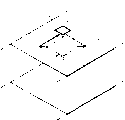
At first see also Fig. 3, shown in Figure 4, the height of the semiconductor chip of the present invention small packaging body that dispels the heat comprises:
One lead frame 1, this lead frame 1 is produced the platform of a recessed chip carrier 11 with etching program, and the hollow-out slot bore 13 that is made as hollow out around this chip carrier 11 only leaves several pieces support belts 12 and is connected to the lead frame main body;
One substrate 3, this substrate 3 can be applicable to the making of high-density line, to reach the demand of high pin number, this substrate 3 fits in this lead frame 1 below, this substrate 3 is provided with high-density line and most foot pad 31 and tin ball 32, and this foot pad 31 is made in hollow-out slot bore 13 positions with respect to lead frame 1, to engage gold thread 22;
One chip 2, this chip 2 is engaged on the chip carrier 11 of lead frame 1 with cement 23 forwards, and with the routing technology with 22 dozens of gold threads on the reservation foot pad 31 on chip foot pad 21 and the substrate 3, to reach the purpose of its function output, and the heat that produces during these chip 2 runnings can distribute through other zones that support belt 12 is transmitted to lead frame 1 by chip carrier 11, reaches the function of high heat radiation;
According to said structure with lead frame 1 with after substrate 3 engages, chip 2 is engaged on the chip carrier 11 of lead frame 1, and 32 in the tin ball that the foot pad 31 and the surface of chip foot pad 21 and substrate 3 is planted with the routing technology is connected conducting with gold thread 22, fills in hollow-out slot bore 13 with sealing 4 at last and coats the part surface zone of gold thread 22 and lead frame 1.
In sum, the present invention integrally combines lead frame and substrate with the microencapsulated technology, makes the overall package body can not need use copper coin or reaches ultra-thin form with heating panel, holds concurrently simultaneously can satisfy high pin and count demand; The heat that produces during the chip running can conduct by lead frame, to reach the effect of high heat radiation.
Claims (1)
1, a kind of height of semiconductor chip small packaging body that dispels the heat comprises a lead frame and a substrate; It is characterized in that:
These lead frame central authorities are provided with recessed mesa-shaped chip carrier, are made as the hollow-out slot bore of hollow out around this chip carrier, only with several pieces support belts chip carrier are connected to lead frame;
This baseplate-laminating is in this lead frame below, and this substrate is provided with high-density line and most foot pad and tin ball;
One chip, this chip is engaged in the chip carrier top of lead frame with cement, and with the foot pad of gold thread connection chip and the foot pad of this substrate, fills in this hollow-out slot bore and coat gold thread and the part surface of lead frame with sealing.
Priority Applications (1)
| Application Number | Priority Date | Filing Date | Title |
|---|---|---|---|
| CNA021431965A CN1484302A (en) | 2002-09-17 | 2002-09-17 | High radiation miniature package for semiconductor chip |
Applications Claiming Priority (1)
| Application Number | Priority Date | Filing Date | Title |
|---|---|---|---|
| CNA021431965A CN1484302A (en) | 2002-09-17 | 2002-09-17 | High radiation miniature package for semiconductor chip |
Publications (1)
| Publication Number | Publication Date |
|---|---|
| CN1484302A true CN1484302A (en) | 2004-03-24 |
Family
ID=34148207
Family Applications (1)
| Application Number | Title | Priority Date | Filing Date |
|---|---|---|---|
| CNA021431965A Pending CN1484302A (en) | 2002-09-17 | 2002-09-17 | High radiation miniature package for semiconductor chip |
Country Status (1)
| Country | Link |
|---|---|
| CN (1) | CN1484302A (en) |
Cited By (4)
| Publication number | Priority date | Publication date | Assignee | Title |
|---|---|---|---|---|
| CN100378933C (en) * | 2005-03-14 | 2008-04-02 | 日月光半导体制造股份有限公司 | Method for manufacturing a semiconductor package with a laminated chip cavity |
| CN100433278C (en) * | 2004-10-29 | 2008-11-12 | 矽品精密工业股份有限公司 | Radiation type packaging structure and its making method |
| CN110446369A (en) * | 2019-07-23 | 2019-11-12 | 中国科学技术大学 | Bonding structure, bonding method and the Package boxes comprising the bonding structure |
| CN110446368A (en) * | 2019-07-23 | 2019-11-12 | 中国科学技术大学 | Bonding structure, bonding method and the Package boxes comprising the bonding structure |
-
2002
- 2002-09-17 CN CNA021431965A patent/CN1484302A/en active Pending
Cited By (4)
| Publication number | Priority date | Publication date | Assignee | Title |
|---|---|---|---|---|
| CN100433278C (en) * | 2004-10-29 | 2008-11-12 | 矽品精密工业股份有限公司 | Radiation type packaging structure and its making method |
| CN100378933C (en) * | 2005-03-14 | 2008-04-02 | 日月光半导体制造股份有限公司 | Method for manufacturing a semiconductor package with a laminated chip cavity |
| CN110446369A (en) * | 2019-07-23 | 2019-11-12 | 中国科学技术大学 | Bonding structure, bonding method and the Package boxes comprising the bonding structure |
| CN110446368A (en) * | 2019-07-23 | 2019-11-12 | 中国科学技术大学 | Bonding structure, bonding method and the Package boxes comprising the bonding structure |
Similar Documents
| Publication | Publication Date | Title |
|---|---|---|
| US6337510B1 (en) | Stackable QFN semiconductor package | |
| US6657311B1 (en) | Heat dissipating flip-chip ball grid array | |
| US6787917B2 (en) | Apparatus for package reduction in stacked chip and board assemblies | |
| US8278150B2 (en) | Stackable packages for three-dimensional packaging of semiconductor dice | |
| US6977439B2 (en) | Semiconductor chip stack structure | |
| JP2936320B2 (en) | Semiconductor package | |
| US8361837B2 (en) | Multiple integrated circuit die package with thermal performance | |
| US7554185B2 (en) | Flip chip and wire bond semiconductor package | |
| TWI420629B (en) | Semiconductor flip chip package | |
| US20070254406A1 (en) | Method for manufacturing stacked package structure | |
| EP1361611A3 (en) | Ball grid array package with stepped stiffener layer | |
| TW200903674A (en) | Copper wire bonding on organic solderability preservative materials | |
| CN101232004A (en) | Chip stack package structure | |
| EP1333490A3 (en) | Ball grid array package with patterned stiffener layer | |
| JP2005317975A (en) | System in package with junction of solder bump and gold bump, and its manufacturing method | |
| KR20050119414A (en) | Stacked package comprising two edge pad-type semiconductor chips and method of manufacturing the same | |
| TW200410380A (en) | Leadless semiconductor packaging structure with inverted flip chip and methods of manufacture | |
| US20060033219A1 (en) | Low profile, chip-scale package and method of fabrication | |
| TW200421587A (en) | Multi-chip module | |
| CN1484302A (en) | High radiation miniature package for semiconductor chip | |
| US20060091516A1 (en) | Flexible leaded stacked semiconductor package | |
| US8021931B2 (en) | Direct via wire bonding and method of assembling the same | |
| US20040183179A1 (en) | Package structure for a multi-chip integrated circuit | |
| WO2004012262A3 (en) | Method for accommodating small minimum die in wire bonded area array packages | |
| US20030160320A1 (en) | High heat dissipation micro-packaging body for semiconductor chip |
Legal Events
| Date | Code | Title | Description |
|---|---|---|---|
| C06 | Publication | ||
| PB01 | Publication | ||
| C10 | Entry into substantive examination | ||
| SE01 | Entry into force of request for substantive examination | ||
| C02 | Deemed withdrawal of patent application after publication (patent law 2001) | ||
| WD01 | Invention patent application deemed withdrawn after publication |