CN1409118A - Acceleration transducer - Google Patents
Acceleration transducer Download PDFInfo
- Publication number
- CN1409118A CN1409118A CN02143502A CN02143502A CN1409118A CN 1409118 A CN1409118 A CN 1409118A CN 02143502 A CN02143502 A CN 02143502A CN 02143502 A CN02143502 A CN 02143502A CN 1409118 A CN1409118 A CN 1409118A
- Authority
- CN
- China
- Prior art keywords
- support arms
- resilient support
- mass fraction
- acceleration transducer
- acceleration
- Prior art date
- Legal status (The legal status is an assumption and is not a legal conclusion. Google has not performed a legal analysis and makes no representation as to the accuracy of the status listed.)
- Pending
Links
Images


Classifications
-
- G—PHYSICS
- G01—MEASURING; TESTING
- G01P—MEASURING LINEAR OR ANGULAR SPEED, ACCELERATION, DECELERATION, OR SHOCK; INDICATING PRESENCE, ABSENCE, OR DIRECTION, OF MOVEMENT
- G01P15/00—Measuring acceleration; Measuring deceleration; Measuring shock, i.e. sudden change of acceleration
-
- G—PHYSICS
- G01—MEASURING; TESTING
- G01P—MEASURING LINEAR OR ANGULAR SPEED, ACCELERATION, DECELERATION, OR SHOCK; INDICATING PRESENCE, ABSENCE, OR DIRECTION, OF MOVEMENT
- G01P15/00—Measuring acceleration; Measuring deceleration; Measuring shock, i.e. sudden change of acceleration
- G01P15/18—Measuring acceleration; Measuring deceleration; Measuring shock, i.e. sudden change of acceleration in two or more dimensions
-
- B—PERFORMING OPERATIONS; TRANSPORTING
- B81—MICROSTRUCTURAL TECHNOLOGY
- B81B—MICROSTRUCTURAL DEVICES OR SYSTEMS, e.g. MICROMECHANICAL DEVICES
- B81B3/00—Devices comprising flexible or deformable elements, e.g. comprising elastic tongues or membranes
- B81B3/0064—Constitution or structural means for improving or controlling the physical properties of a device
- B81B3/0067—Mechanical properties
- B81B3/0078—Constitution or structural means for improving mechanical properties not provided for in B81B3/007 - B81B3/0075
-
- G—PHYSICS
- G01—MEASURING; TESTING
- G01P—MEASURING LINEAR OR ANGULAR SPEED, ACCELERATION, DECELERATION, OR SHOCK; INDICATING PRESENCE, ABSENCE, OR DIRECTION, OF MOVEMENT
- G01P15/00—Measuring acceleration; Measuring deceleration; Measuring shock, i.e. sudden change of acceleration
- G01P15/02—Measuring acceleration; Measuring deceleration; Measuring shock, i.e. sudden change of acceleration by making use of inertia forces using solid seismic masses
- G01P15/08—Measuring acceleration; Measuring deceleration; Measuring shock, i.e. sudden change of acceleration by making use of inertia forces using solid seismic masses with conversion into electric or magnetic values
- G01P15/0802—Details
-
- G—PHYSICS
- G01—MEASURING; TESTING
- G01P—MEASURING LINEAR OR ANGULAR SPEED, ACCELERATION, DECELERATION, OR SHOCK; INDICATING PRESENCE, ABSENCE, OR DIRECTION, OF MOVEMENT
- G01P15/00—Measuring acceleration; Measuring deceleration; Measuring shock, i.e. sudden change of acceleration
- G01P15/02—Measuring acceleration; Measuring deceleration; Measuring shock, i.e. sudden change of acceleration by making use of inertia forces using solid seismic masses
- G01P15/08—Measuring acceleration; Measuring deceleration; Measuring shock, i.e. sudden change of acceleration by making use of inertia forces using solid seismic masses with conversion into electric or magnetic values
- G01P15/12—Measuring acceleration; Measuring deceleration; Measuring shock, i.e. sudden change of acceleration by making use of inertia forces using solid seismic masses with conversion into electric or magnetic values by alteration of electrical resistance
- G01P15/123—Measuring acceleration; Measuring deceleration; Measuring shock, i.e. sudden change of acceleration by making use of inertia forces using solid seismic masses with conversion into electric or magnetic values by alteration of electrical resistance by piezo-resistive elements, e.g. semiconductor strain gauges
-
- B—PERFORMING OPERATIONS; TRANSPORTING
- B81—MICROSTRUCTURAL TECHNOLOGY
- B81B—MICROSTRUCTURAL DEVICES OR SYSTEMS, e.g. MICROMECHANICAL DEVICES
- B81B2201/00—Specific applications of microelectromechanical systems
- B81B2201/02—Sensors
- B81B2201/0228—Inertial sensors
- B81B2201/0235—Accelerometers
-
- B—PERFORMING OPERATIONS; TRANSPORTING
- B81—MICROSTRUCTURAL TECHNOLOGY
- B81B—MICROSTRUCTURAL DEVICES OR SYSTEMS, e.g. MICROMECHANICAL DEVICES
- B81B2203/00—Basic microelectromechanical structures
- B81B2203/01—Suspended structures, i.e. structures allowing a movement
- B81B2203/0109—Bridges
-
- B—PERFORMING OPERATIONS; TRANSPORTING
- B81—MICROSTRUCTURAL TECHNOLOGY
- B81B—MICROSTRUCTURAL DEVICES OR SYSTEMS, e.g. MICROMECHANICAL DEVICES
- B81B2203/00—Basic microelectromechanical structures
- B81B2203/05—Type of movement
- B81B2203/053—Translation according to an axis perpendicular to the substrate
-
- B—PERFORMING OPERATIONS; TRANSPORTING
- B81—MICROSTRUCTURAL TECHNOLOGY
- B81B—MICROSTRUCTURAL DEVICES OR SYSTEMS, e.g. MICROMECHANICAL DEVICES
- B81B2203/00—Basic microelectromechanical structures
- B81B2203/05—Type of movement
- B81B2203/058—Rotation out of a plane parallel to the substrate
-
- G—PHYSICS
- G01—MEASURING; TESTING
- G01P—MEASURING LINEAR OR ANGULAR SPEED, ACCELERATION, DECELERATION, OR SHOCK; INDICATING PRESENCE, ABSENCE, OR DIRECTION, OF MOVEMENT
- G01P15/00—Measuring acceleration; Measuring deceleration; Measuring shock, i.e. sudden change of acceleration
- G01P15/02—Measuring acceleration; Measuring deceleration; Measuring shock, i.e. sudden change of acceleration by making use of inertia forces using solid seismic masses
- G01P15/08—Measuring acceleration; Measuring deceleration; Measuring shock, i.e. sudden change of acceleration by making use of inertia forces using solid seismic masses with conversion into electric or magnetic values
- G01P2015/0805—Measuring acceleration; Measuring deceleration; Measuring shock, i.e. sudden change of acceleration by making use of inertia forces using solid seismic masses with conversion into electric or magnetic values being provided with a particular type of spring-mass-system for defining the displacement of a seismic mass due to an external acceleration
- G01P2015/0822—Measuring acceleration; Measuring deceleration; Measuring shock, i.e. sudden change of acceleration by making use of inertia forces using solid seismic masses with conversion into electric or magnetic values being provided with a particular type of spring-mass-system for defining the displacement of a seismic mass due to an external acceleration for defining out-of-plane movement of the mass
- G01P2015/084—Measuring acceleration; Measuring deceleration; Measuring shock, i.e. sudden change of acceleration by making use of inertia forces using solid seismic masses with conversion into electric or magnetic values being provided with a particular type of spring-mass-system for defining the displacement of a seismic mass due to an external acceleration for defining out-of-plane movement of the mass the mass being suspended at more than one of its sides, e.g. membrane-type suspension, so as to permit multi-axis movement of the mass
- G01P2015/0842—Measuring acceleration; Measuring deceleration; Measuring shock, i.e. sudden change of acceleration by making use of inertia forces using solid seismic masses with conversion into electric or magnetic values being provided with a particular type of spring-mass-system for defining the displacement of a seismic mass due to an external acceleration for defining out-of-plane movement of the mass the mass being suspended at more than one of its sides, e.g. membrane-type suspension, so as to permit multi-axis movement of the mass the mass being of clover leaf shape
Abstract
A microminiature and thin semiconductor acceleration sensor with high sensitivity is provided. The acceleration sensor has a mass portion formed in a center part of a silicon semiconductor substrate, a frame formed at a perimeter portion of the substrate, thin elastic support arms, which are provided at upper part of the mass portion and the frame and connect the mass portion and the frame, and a plurality of pairs of piezoresistors disposed on top surface sides of the elastic support arms. In the mass portion, a plurality of recessed portions which are recessed toward a center thereof from a perimeter thereof are formed, each of the elastic support arms is attached to the top surface of the mass portion at the bottom of each of the recessed portions, and sides of the elastic support arms are spaced from sides of the recessed portions. Since the volume of the mass portion and the length of the elastic support arms can be independently made large, sensitivity can be made higher.
Description
Background of invention
1, invention field
The present invention relates to a kind of acceleration transducer, be used for surveying acceleration, can be used for toy, automobile, aircraft, portable terminal or the like relates in particular to a kind of acceleration transducer that can use semiconductor technology to make.
2, related process is described
Utilize the acceleration transducer of the change of the Change Example of physical quantity such as piezoresistance effect and electrostatic capacitance to have grown up and commercialization.These acceleration transducers can be widely used in various fields, but recently, need can survey the acceleration of multiaxis direction so simultaneously and have the small size acceleration transducer of high sensitivity.
Since silicon single crystal since minimum lattice imperfection becomes modification that desirable elastic body and semiconductor process techniques needn't be big can be applied to this since, piezoresistance effect N-type semiconductor N acceleration transducer has received increasing attention, wherein a thin resiliency supported partly is positioned on the silicon monocrystalline substrate, for example be applied to thin resiliency supported pressure partly by strainmeter, the piezoresistance effect element converts electric signal and output to.
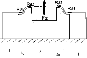
As a common 3-axis acceleration sensor, there is one openly, for example, at Japanese publication No.63-169078, its vertical view is presented among Figure 15, and the sectional view that the XVI-XVI line in Figure 15 is got is presented among Figure 16, and skeleton view is presented among Figure 17.Acceleration transducer 100 has many resilient support arms 130, and each all has girder construction, is made up of one of silicon monocrystalline substrate thin part.In the centre one mass fraction 120 is arranged, it is made up of one of silicon monocrystalline substrate thick part, is coupled together by resilient support arms 130 with framework 110 at its edge.Each direction of principal axis in resilient support arms 130 forms many strainmeters 140.
With reference to Figure 15, Figure 16 and Figure 17 can explain one-piece construction.Sensor 100 has the mass fraction of being made up of the thick part of silicon monocrystalline substrate 120, framework 110 is placed around mass fraction 120, two pairs of resilient support arms 130 have the form of beam, they orthogonal and each all forms also quality of connection part 120 and framework 110 by the thin part of silicon monocrystalline substrate.When working sensor, this mass fraction moves in framework so that therefore the resilient support arms distortion is out of shape the strainmeter that is positioned on the resilient support arms and is detected to obtain the acceleration of work.Acceleration in Figure 15 on the X-direction is measured by four strainmeters 140 that are positioned on the resilient support arms that X-direction is extended, and the acceleration on the Y direction is measured by four strainmeters 140 that are positioned on the resilient support arms that Y direction is extended.Acceleration on the Z-direction relies on all strainmeters 140 to obtain measuring.By in the silicon monocrystalline substrate of size, making four L shaped through holes 150 with framework 110, form middle mass fraction 120, be positioned at the framework 110 at edge and the sway brace 130 that is connected them, and by making support arm portion thin, acceleration transducer is constructed to such an extent that can be out of shape and have high sensitivity.
In acceleration transducer described above, in order to strengthen sensitivity, thereby effective way is the quality that the volume of increase mass fraction 120 increases it, perhaps increase the length of resilient support arms 130, as well-known, the increase of sensitivity is proportional with the length of the quality of mass fraction and sway brace fully.In other words, the volume of mass fraction 120 increases, and perhaps the length of resilient support arms 130 increases, so become more easy deformation and pressure of resilient support arms 130 can more effectively be delivered to strainmeter, has therefore increased sensitivity.Yet, increase mass fraction 120 and increase the length of resilient support arms 130 conflicting, and particularly wafer size remain under the condition of constant or plan when reducing size they two mutual incompatible.That is to say that if mass fraction 120 becomes bigger, the length of resilient support arms 130 becomes shorter, many raisings of sensitivity can not be improved so.Therefore, glass sheet or the like all sticks on the volume (just, weight) of the rear surface of mass fraction 120 with the part 120 that improves the quality in assembling process, has therefore improved sensitivity.The length of resilient support arms 130 can not be done very greatly, but wafer does more at thickness direction (thickness direction of silicon monocrystalline substrate), thereby the quality that has therefore increased mass fraction 120 has been strengthened sensitivity.Therefore, can not realize highly sensitive small-sized and thin acceleration transducer usually.
Abstract of invention
The present invention considers situation described above, and its purpose is to solve a difficult problem described above and a kind of small-sized and thin acceleration transducer that can improve sensitivity is provided.
In order to solve the problem described above, the present invention adopts following acceleration transducer.That is to say that acceleration transducer of the present invention has mass fraction in the centre; Thick framework around mass fraction has default distance to mass fraction; Strainmeter is distributed on the resilient support arms, many recesses, they are recessed to its center from the edge of mass fraction, be formed in the mass fraction, each resilient support arms is connected with the upper surface of mass fraction in the bottom surface of each recess, and each side of resilient support arms is separated with each side of recess.
In above-mentioned acceleration transducer, preferably acceleration transducer has four resilient support arms, in their four resilient support arms two other two quadratures with resilient support arms.Two resilient support arms separately that preferably make simultaneously four resilient support arms are linear array all.Preferably make along the longitudinal direction of resilient support arms and survey the strainmeter of acceleration and be positioned at along the strainmeter of upper surface orientation detection acceleration on two of linearly aligned resilient support arms.
Acceleration transducer preferably of the present invention is made by a SOI wafer, and these resilient support arms are by a SiO
2A layer and a silicon layer are formed.
In acceleration transducer of the present invention, when acceleration was operated in the acceleration transducer, the displacement of mass fraction was in proportion with acceleration on the direction of acceleration.Resilient support arms, it is positioned at the periphery of mass fraction to stretch out, and a corresponding special direction bending of the displacement with mass fraction, and simultaneously, a plurality of strainmeters that are positioned on the resilient support arms are also crooked.Therefore, the resistance value of strainmeter changes owing to these are crooked, and if be provided at by four strainmeters by the detection circuit that full bridge diagram is formed on each the direction and constitute, can obtain so to export corresponding to the voltage of the amount of bow that applies.
In acceleration transducer of the present invention, in mass fraction, the recess of two pairs of basic one-tenth rectangular parallelepiped protrusion part, just, recess, its width is greater than the width of resilient support arms, and is recessed to the center from the edge of mass fraction corresponding to the both direction of X and Y direction, and mass fraction is connected with two pairs of resilient support arms in the upper surface side of recess.The volume of mass fraction and the length of resilient support arms can be in the scope of the necessary and sufficient condition of the performance of this sensor independent design.That is to say that two design parameters promptly for the volume of the part that improves the quality and the parameter of the length that improves resilient support arms, can freely determine, and therefore can realize high sensitivity in little and thin component structure.
The accompanying drawing summary:
Fig. 1 is the vertical view that shows the acceleration transducer of first embodiment of the present invention;
Fig. 2 is the upward view of the acceleration transducer among Fig. 1;
Fig. 3 is the sectional view that the acceleration transducer among Fig. 1 is got along the III-III line among Fig. 1;
Fig. 4 is the skeleton view of the acceleration transducer among Fig. 1;
Fig. 5 is the curve map of relation of volume that has shown the mass fraction of sensitivity and acceleration transducer of the present invention;
Fig. 6 is the curve map of relation of length that has shown the resilient support arms of sensitivity and acceleration transducer of the present invention;
Fig. 7 is the curve map of relation of width that has shown the resilient support arms of sensitivity and acceleration transducer of the present invention;
Fig. 8 is the curve map of relation of thickness that has shown the resilient support arms of sensitivity and acceleration transducer of the present invention;
Fig. 9 has explained when the synoptic diagram of acceleration in the distortion of X-axis (Y-axis) direction work brief acceleration sensor;
Figure 10 has shown the example of bridge circuit of the acceleration of measured X axle (Y-axis) direction;
Figure 11 has explained when the synoptic diagram of acceleration in the distortion of Z-direction work brief acceleration sensor;
Figure 12 has shown the example of the bridge circuit of the acceleration of measuring Z-direction;
Figure 13 has shown that the acceleration transducer of embodiments of the present invention is in the production run of A to E;
Figure 14 is the vertical view that has shown the acceleration transducer of another embodiment of the present invention;
Figure 15 is the vertical view that has shown the acceleration transducer of announcing in Japanese publication;
Figure 16 is the sectional view that the acceleration transducer among Figure 15 is got along the XVI-XVI line among Figure 15; With
Figure 17 is the skeleton view of the acceleration transducer among Figure 15.
Embodiment describes in detail
Each embodiment of the present invention will be explained below.
To use Fig. 1, Fig. 2 and Fig. 3 explain first embodiment of the present invention.Fig. 1 is the vertical view of semiconductor acceleration sensor of the present invention, and Fig. 2 is the planimetric map according to the acceleration transducer of the embodiments of the present invention that show among Fig. 1, and it sees that from below Fig. 3 is the sectional view of getting along III-III line (X-axis) among Fig. 1.
Acceleration transducer of the present invention uses a silicon monocrystalline substrate, passes through SiO
2Insulation course forms soi layer, and just, a SOI wafer becomes possibility in order to make the thickness of controlling resilient support arms accurately.SOI is the abbreviation of the silicon on the insulator.In this example, by sparsely forming SiO
2The etching that insulation course and the wafer that forms become on the Si wafer of the about 550 μ m of a thickness stops (about 1 μ m), has formed the N type silicon single crystal layer of thick 10 μ m on this wafer, and so the wafer that forms uses as substrate.The acceleration transducer of present embodiment is made up of these parts: center one mass fraction 2, and it is made up of one of silicon monocrystalline substrate thick part; Be placed on mass fraction 2 quadra 1 to surround it on every side; Two couples of beam shape resilient support arms 3a, 3b, 3c and 3d, they are made up of with quality of connection part 2 and framework 1 the thin part of silicon monocrystalline substrate, strainmeter is (in ensuing explanation, " voltage dependent resistor (VDR) " is the example that strainmeter uses, therefore they are known as " voltage dependent resistor (VDR) ") 11,12 ..., 33,34, in them four are used for each axle, and they are positioned on the resilient support arms, corresponding to mutually perpendicular two detection axis (X and Y-axis) be orthogonal to the detection axis (Z axle) of the upper surface of acceleration transducer.That is to say that two voltage dependent resistor (VDR)s 13 and 14 and two voltage dependent resistor (VDR)s 11 and 12 are positioned at separately along X-direction resilient support arms 3a and 3c and go up to survey the acceleration on the X-direction.Two voltage dependent resistor (VDR)s 21 and 22 and two voltage dependent resistor (VDR)s 23 and 24 are positioned at the resilient support arms 3b and the 3d that extend along Y direction separately and go up to survey the acceleration on the Y direction.Two voltage dependent resistor (VDR)s 33 and 34 and two voltage dependent resistor (VDR)s 31 and 32 are positioned at the resilient support arms 3a and the 3c that extend along X-direction separately and go up to survey the acceleration of Z-direction.In this example, the voltage dependent resistor (VDR) that the acceleration on the Z direction is positioned on resilient support arms 3a and the 3c is surveyed, but the element of surveying the acceleration on the Z-direction can be positioned on resilient support arms 3b and the 3d.Four resistance surveying in the voltage dependent resistor (VDR) of the acceleration on each direction are formed a whole bridge detection circuit.
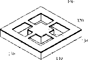
In mass fraction 2, form many recesses 51, just, from the edge to the recessed notch part in center.In the present embodiment, each recess 51 is all along the center of the middle mind-set mass fraction of each side of square mass fraction 2 and form.Here recess is the shape of rectangular parallelepiped protrusion part, and an end of resilient support arms links to each other with the upper surface of mass fraction in the bottom of recess, and the other end of resilient support arms links to each other with the upper surface of thick framework, and mass fraction and thick framework are with the resilient support arms bridge joint.Each side of the resilient support arms that is positioned at each recess is separated with each side of recess.
To be convenient to more understand in order making, in Fig. 4, to have shown synoptic diagram according to sensor construction of the present invention.Provide with identical parameter symbol in Fig. 4 as composition identical among Fig. 1 to 3.In Fig. 4 obviously, by adopting structure of the present invention, volume and resilient support arms 3a that can independent control of quality part 2,3b, the length of 3c and 3d.Just, resilient support arms 3a, 3b, 3c and 3d do thinly and are long as far as possible, and mass fraction 2 is done greatly as far as possible, so the detection sensitivity of sensor can improve.
Here, with the volume of research mass fraction and the length of resilient support arms, width and thickness, they are all influential to the sensitivity of acceleration transducer, and this, problem just of the present invention.As the relation of the volume (quality) of the sensitivity of the acceleration transducer that shows among Fig. 5 and mass fraction, the volume of sensitivity and mass fraction (quality) is proportional, doubles as fruit volume, and sensitivity doubles.The relation of the sensitivity of acceleration transducer and the length of resilient support arms is presented among Fig. 6.The length of sensitivity and resilient support arms is proportional.Fig. 5 has shown the comparison of supposing that other condition is identical with Fig. 6.In the present invention, recess or recess are provided on the mass fraction so that resilient support arms is longer, and the volume of mass fraction can do more.For this purpose, according to acceleration transducer of the present invention, when chip size is made constant, even be fixed on current state following time when the length of resilient support arms, can not increase the thickness of chip and make the volume of mass fraction 2 can accomplish 2 times or bigger easily, and that sensitivity can be brought up to this is proportional.Further, be easy to make that notch part is bigger and make the length of resilient support arms become 1.5 times of present length or more, and in this case mass fraction 2 volume reduce very little.The increase of sensitivity is almost proportional with the length of elastic part.The degree of depth of the recess by optimizing mass fraction, not desensitization and make chip size littler.
As a reference, the relation between the width of sensitivity and resilient support arms, and the relation between the thickness of sensitivity and resilient support arms is presented among Fig. 7 and Fig. 8 separately.It is to understand easily that width that resilient support arms is littler and thickness are suitable for increasing sensitivity.
Explanation is positioned at the function of the voltage dependent resistor (VDR) of resilient support arms here.Voltage dependent resistor (VDR) 11 and 12 are provided for the resilient support arms 3c and the 3a that extend along X-direction, and 13 and 14, be used for testing the acceleration on the X-direction.Voltage dependent resistor (VDR) 21 and 22 are provided for the resilient support arms 3d and the 3b that extend along Y direction, and 23 and 24, be used for testing the acceleration on the Y direction.Voltage dependent resistor (VDR) 31 and 32 are provided for the resilient support arms 3c and the 3a that extend along X-direction, and 33 and 34, be used for testing the acceleration on the Z-direction.
When the acceleration on the X-direction was added on the mass fraction 2, power Fx acted on the center of the gravity of mass fraction 2, and therefore as shown in Figure 9, the left side of the upper surface of mass fraction 2 moves down, and the right side of its upper surface moves up.As a result, be in voltage dependent resistor (VDR) 11 expansions on the resilient support arms 3a, and voltage dependent resistor (VDR) 12 is shunk.Be in voltage dependent resistor (VDR) 13 expansions on the resilient support arms 3a, and voltage dependent resistor (VDR) 14 is shunk.Since such expansion of voltage dependent resistor (VDR) and contraction, resistance R 11, R12, R13 and R14 have changed.When the resistance junction of voltage dependent resistor (VDR) synthesizes a full bridge diagram and normal pressure Vin when being applied to it, as shown in figure 10, the change that can measure the resistance of voltage dependent resistor (VDR) according to output Vout.As for the acceleration of Y direction, the resilient support arms of extending along Y direction can be enough with consider in the identical mode of X-direction.
When the acceleration on the Z-direction is added on the mass fraction 2, power Fz effect, the left side and the right side of the upper surface of mass fraction 2 move up, as shown in figure 11.As a result, the voltage dependent resistor (VDR) 31 that is on the resilient support arms 3c is shunk, and voltage dependent resistor (VDR) 32 expansions.In an identical manner, be in voltage dependent resistor (VDR) 33 expansions on the resilient support arms 3a, and voltage dependent resistor (VDR) 34 is shunk.When the resistance R 11 of voltage dependent resistor (VDR), R12, R13 and R14 are combined into a whole bridge circuit and normal pressure Vin when being applied to it, as shown in figure 12, and the change that can measure the resistance of voltage dependent resistor (VDR) according to output Vout.The electric wire that also is suitable for changing the resistance in the bridge circuit from those of the bridge circuit of the acceleration of surveying X-direction connect connects the acceleration of surveying on the Z-direction, therefore also uses other voltage dependent resistor (VDR).
To explain a kind of production method of present embodiment below.Figure 13 has shown that the part (left-half) in a cross section (III-III cross section) of the X-direction among Fig. 1 is used for explaining main technique.As described above, the SOI wafer is a Si single crystalline substrate, by Si substrate 60, and the soi layer 80 on the upper surface, (it is a Si active layer) and a SiO
2Layer 70, (it is between Si substrate 60 and the soi layer 80 and as etching and stops use) constitutes, and be represented as the label among Figure 13.As their thickness, Si substrate 60 thick 500 μ m are to 625 μ m, SiO
2Bed thickness 1 μ m and the thick about 10 μ m of soi layer.
The first step of production technology is to do the figure of a default form, and photoresist or thermal oxide SiO are arranged on the surface of its soi layer 80
2Film or the like, and make voltage dependent resistor (VDR) 11 and 12, by impurity diffusion technology for example ion inject (Figure 13) and carry out boron diffusion.As surface impurity density,, adopt about 2 * 10 from temperature characterisitic and two angles of sensitivity
18Atom/cm
3
Then, in order to protect voltage dependent resistor (VDR) 11 and 12, make layer protecting film 41 (Figure 13 B).As diaphragm 41, use the SiO that in semiconductor technology, uses usually
2And PSG (phosphosilicate glass) multilayer film, ion is movably played the getter effect.Replace SiO
2With the two membranes of PSG, can use SiO
2Two membranes with GaN.According to high sensitivity, preferably the thickness of diaphragm 41 is done thinly as far as possible reducing pressure, thus it do 0.3 μ m to 0.5 μ m.
Then, by the wet etching of hydrofluorite as principal ingredient.In diaphragm 41, on the two ends of voltage dependent resistor (VDR) 11 and 12, form the through hole 40a (Figure 13 C) of connection electrode.
Then, in order to make electrode wires, form aluminium alloy film (aluminium, copper, silicon or the like are principal ingredients) by sputter.Thickness is that 0.3 μ m is to 0.5 μ m.Lead-in wire electrode (lead electrode) 40 forms (Figure 13 D) by photoetching.
Then, though do not show, by dry etching or other similar approach corrosion soi layer 80, to form the thin part that shows in the via hole image 5 to Fig. 1.
Then, on rear surface in the substrate 60, the photoresist mask that forms has the shape of mass fraction 2 and framework 1, use two-sided adjustment device to adjust logical voltage dependent resistor (VDR) 11 and 12 simultaneously, the position of via hole image 5 of arrival soi layer 80 or the like, come etching substrate 60 by dry etching, and as the SiO of inhibition of corrosion
2Layer 70 is disposed (Figure 13 E) by wet etching.As etchant solution, use buffered hydrofluoric acid.The shape of this process photoresist mask is made such shape, at resilient support arms 3a, and 3b, on four sides of square mass fraction, there is the recess of rectangle in the place that 3c is connected with 3d. Resilient support arms 3a, 3b, 3c and 3d form in this dry etching process, in some cases, preferably allow SiO
2Layer 70 stops as etching and it is not disposed, and purpose is the balance that keeps whole pressure, at the remaining SiO of the rear side of resilient support arms
2It can be suitable that the part of layer 70 stops as etching.
Then, by using cutter or similar tool, the many acceleration sensor element a slice a slices that are formed on the wafer are cut into sensor chip, for example encapsulate or the like by assembly technology, have finished semiconductor acceleration sensor.
The acceleration transducer of another embodiment of the present invention is presented among Figure 14.Figure 14 is the planimetric map of the front side of sensor, provides with identical label and symbol with components identical among Fig. 1, so that understand.In this embodiment, in mass fraction 2, its corner is made curved surface along the four direction extension as four-leaf clover, and four corner portions located of framework 1 are made into curved surface simultaneously.When in the production technology that Figure 13 describes, mass fraction 2 being carried out dry etching, difference by reducing the graphic width size also improves flowing of etching air-flow, this embodiment has the conforming effect of the etching speed of raising, it is as the distinctive effect of this embodiment, also explain in first embodiment as described above simultaneously like that, have to make sensor do compactly and thin and strengthen the such effect of sensitivity.The physical strength of frame part also can improve.
In first and second embodiments of describing so far, the via hole image 5 that forms in soi layer 80 is of similar shape with the pattern of disposing by break-through-etch from the rear side of wafer when forming mass fraction 2 by etching substrate 60, but they are not to meet each other, and as long as mass fraction 2 and resilient support arms 3a, 3b, 3c and 3d, and framework 1 isolates, and also is fine.Arrive the via hole image 5 of soi layer 80 and the graphics shape of mass fraction 2, except aforementioned first and second embodiments, various considerations can be arranged.Just, as the shape of mass fraction 2 and framework 1, can consider various shapes, they are not limited to the shape of aforementioned embodiments.
Claims (6)
1. acceleration transducer comprises:
Be in the mass fraction at center;
Around the webbing frame of mass fraction, it has a default distance to mass fraction;
A plurality of resilient support arms, upper surface of bridge joint mass fraction and webbing frame; And
Be arranged in the strainmeter on the resilient support arms,
Wherein a plurality of recesses are formed in the mass fraction, they are recessed to the center of mass fraction from the periphery of mass fraction, each resilient support arms is connected with the upper surface of mass fraction in the bottom of each recess, and each side of resilient support arms is separated with each side of recess.
2. according to the acceleration transducer of claim 1, wherein acceleration transducer has four resilient support arms, in its resilient support arms two other two quadratures with resilient support arms.
3. according to the acceleration transducer of claim 2, two linear array separately of four resilient support arms wherein.
4. according to the acceleration transducer of claim 3, the strainmeter of wherein surveying the strainmeter of the acceleration on the longitudinal direction of resilient support arms and surveying the acceleration on the upper surface direction is arranged on linearly aligned two resilient support arms.
5. according to the acceleration transducer of claim 3, wherein acceleration transducer is made by a SOI wafer, and these a plurality of resilient support arms are by a SiO
2A layer and a silicon layer constitute.
6. according to the acceleration transducer of claim 4, wherein acceleration transducer is made by a SOI wafer, and these a plurality of resilient support arms are by a SiO
2A layer and a silicon layer constitute.
Applications Claiming Priority (4)
| Application Number | Priority Date | Filing Date | Title |
|---|---|---|---|
| JP293526/2001 | 2001-09-26 | ||
| JP2001293526 | 2001-09-26 | ||
| JP363371/2001 | 2001-11-28 | ||
| JP2001363371A JP2003172745A (en) | 2001-09-26 | 2001-11-28 | Semiconductor acceleration sensor |
Publications (1)
| Publication Number | Publication Date |
|---|---|
| CN1409118A true CN1409118A (en) | 2003-04-09 |
Family
ID=26622909
Family Applications (1)
| Application Number | Title | Priority Date | Filing Date |
|---|---|---|---|
| CN02143502A Pending CN1409118A (en) | 2001-09-26 | 2002-09-26 | Acceleration transducer |
Country Status (5)
| Country | Link |
|---|---|
| US (1) | US20030057447A1 (en) |
| EP (1) | EP1298442A1 (en) |
| JP (1) | JP2003172745A (en) |
| KR (1) | KR20030026872A (en) |
| CN (1) | CN1409118A (en) |
Cited By (6)
| Publication number | Priority date | Publication date | Assignee | Title |
|---|---|---|---|---|
| CN100373161C (en) * | 2003-09-16 | 2008-03-05 | 日立金属株式会社 | Acceleration sensor |
| CN1873421B (en) * | 2005-05-30 | 2010-06-02 | 冲电气工业株式会社 | Semiconductor acceleration sensor device and fabrication method thereof |
| CN102967729A (en) * | 2012-09-18 | 2013-03-13 | 华东光电集成器件研究所 | Piezoresistive micro-electromechanical system (MEMS) accelerometer |
| CN104919293A (en) * | 2012-12-06 | 2015-09-16 | 株式会社村田制作所 | Piezoresistive mems sensor |
| CN107963095A (en) * | 2017-11-23 | 2018-04-27 | 交控科技股份有限公司 | Vehicle-wheel speed sensor, detection device and axle condition detection method |
| WO2021042316A1 (en) * | 2019-09-05 | 2021-03-11 | 深圳市柔宇科技有限公司 | Acceleration sensor |
Families Citing this family (9)
| Publication number | Priority date | Publication date | Assignee | Title |
|---|---|---|---|---|
| EP1491901A1 (en) | 2003-06-25 | 2004-12-29 | Matsushita Electric Works, Ltd. | Semiconductor acceleration sensor and method of manufacturing the same |
| JP2006275896A (en) * | 2005-03-30 | 2006-10-12 | Yokohama Rubber Co Ltd:The | Semiconductor acceleration sensor |
| JP4747677B2 (en) * | 2005-05-27 | 2011-08-17 | 大日本印刷株式会社 | Manufacturing method of angular velocity sensor |
| ITTO20070033A1 (en) * | 2007-01-19 | 2008-07-20 | St Microelectronics Srl | Z AXIS MICROELETTROMECHANICAL DEVICE WITH PERFECT ARREST STRUCTURE |
| JP4838229B2 (en) | 2007-07-27 | 2011-12-14 | トレックス・セミコンダクター株式会社 | Accelerometer |
| JP5652775B2 (en) | 2009-05-29 | 2015-01-14 | トレックス・セミコンダクター株式会社 | Acceleration sensor element and acceleration sensor having the same |
| JP6294463B2 (en) | 2014-03-20 | 2018-03-14 | 京セラ株式会社 | Sensor |
| WO2016120213A1 (en) | 2015-01-26 | 2016-08-04 | Cirrus Logic International Semiconductor Limited | Mems devices and processes |
| CN105021846B (en) * | 2015-07-06 | 2018-04-17 | 西安交通大学 | A kind of six axis one type micro acceleration sensors and preparation method thereof |
Family Cites Families (11)
| Publication number | Priority date | Publication date | Assignee | Title |
|---|---|---|---|---|
| JP2940293B2 (en) * | 1992-03-31 | 1999-08-25 | 日産自動車株式会社 | Manufacturing method of semiconductor acceleration sensor |
| EP0567075B1 (en) * | 1992-04-22 | 2001-10-24 | Denso Corporation | A method for producing semiconductor device |
| JP2776142B2 (en) * | 1992-05-15 | 1998-07-16 | 株式会社日立製作所 | Acceleration sensor |
| JPH06148229A (en) * | 1992-11-04 | 1994-05-27 | Fujikura Ltd | Semiconductor acceleration sensor |
| JP2639308B2 (en) * | 1992-11-19 | 1997-08-13 | 富士電機株式会社 | Force sensor, temperature sensor and temperature / force sensor device |
| JPH08107219A (en) * | 1994-10-04 | 1996-04-23 | Seiko Instr Inc | Semiconductor acceleration sensor and its manufacture |
| JP3305516B2 (en) * | 1994-10-31 | 2002-07-22 | 株式会社東海理化電機製作所 | Capacitive acceleration sensor and method of manufacturing the same |
| FR2742230B1 (en) * | 1995-12-12 | 1998-01-09 | Sextant Avionique | ACCELEROMETER AND MANUFACTURING METHOD |
| US5894090A (en) * | 1996-05-31 | 1999-04-13 | California Institute Of Technology | Silicon bulk micromachined, symmetric, degenerate vibratorygyroscope, accelerometer and sensor and method for using the same |
| WO1998037425A1 (en) * | 1997-02-21 | 1998-08-27 | Matsushita Electric Works, Ltd. | Acceleration sensor element and method of its manufacture |
| US6196067B1 (en) * | 1998-05-05 | 2001-03-06 | California Institute Of Technology | Silicon micromachined accelerometer/seismometer and method of making the same |
-
2001
- 2001-11-28 JP JP2001363371A patent/JP2003172745A/en active Pending
-
2002
- 2002-09-16 US US10/243,650 patent/US20030057447A1/en not_active Abandoned
- 2002-09-18 EP EP02021223A patent/EP1298442A1/en not_active Withdrawn
- 2002-09-24 KR KR1020020057700A patent/KR20030026872A/en not_active Application Discontinuation
- 2002-09-26 CN CN02143502A patent/CN1409118A/en active Pending
Cited By (7)
| Publication number | Priority date | Publication date | Assignee | Title |
|---|---|---|---|---|
| CN100373161C (en) * | 2003-09-16 | 2008-03-05 | 日立金属株式会社 | Acceleration sensor |
| CN1873421B (en) * | 2005-05-30 | 2010-06-02 | 冲电气工业株式会社 | Semiconductor acceleration sensor device and fabrication method thereof |
| CN102967729A (en) * | 2012-09-18 | 2013-03-13 | 华东光电集成器件研究所 | Piezoresistive micro-electromechanical system (MEMS) accelerometer |
| CN104919293A (en) * | 2012-12-06 | 2015-09-16 | 株式会社村田制作所 | Piezoresistive mems sensor |
| CN107963095A (en) * | 2017-11-23 | 2018-04-27 | 交控科技股份有限公司 | Vehicle-wheel speed sensor, detection device and axle condition detection method |
| WO2021042316A1 (en) * | 2019-09-05 | 2021-03-11 | 深圳市柔宇科技有限公司 | Acceleration sensor |
| CN113366321A (en) * | 2019-09-05 | 2021-09-07 | 深圳市柔宇科技股份有限公司 | Acceleration sensor |
Also Published As
| Publication number | Publication date |
|---|---|
| JP2003172745A (en) | 2003-06-20 |
| EP1298442A1 (en) | 2003-04-02 |
| KR20030026872A (en) | 2003-04-03 |
| US20030057447A1 (en) | 2003-03-27 |
Similar Documents
| Publication | Publication Date | Title |
|---|---|---|
| CN1273836C (en) | Acceleration sensor | |
| CN1409118A (en) | Acceleration transducer | |
| JP3457037B2 (en) | Integrated accelerometer | |
| US4553436A (en) | Silicon accelerometer | |
| US5081867A (en) | Semiconductor sensor | |
| US5239870A (en) | Semiconductor acceleration sensor with reduced cross axial sensitivity | |
| KR100715644B1 (en) | Acceleration sensor | |
| CN102023234B (en) | Micromachined accelerometer with monolithic electrodes and method of making the same | |
| US5404749A (en) | Boron doped silicon accelerometer sense element | |
| CN101038298A (en) | Symmetrical straight beam structure condenser type micro-acceleration sensor and manufacturing method thereof | |
| JP4335545B2 (en) | Sensor for detecting both pressure and acceleration and manufacturing method thereof | |
| US7111514B2 (en) | Acceleration sensor | |
| US6763719B2 (en) | Acceleration sensor | |
| CN107643424B (en) | Piezoresistive MEMS acceleration chip and manufacturing method thereof | |
| CN114061797B (en) | MEMS piezoresistive pressure sensor with double-bridge structure and preparation method thereof | |
| CN100422697C (en) | Acceleration transducer | |
| JP2002529684A (en) | Strain measuring instrument | |
| JPH05340956A (en) | Acceleration sensor | |
| JPH08211091A (en) | Semiconductor acceleration detecting device | |
| CN116678544B (en) | Silicon strain gauge and manufacturing method thereof | |
| JPH1144705A (en) | Semiconductor acceleration sensor and its manufacture | |
| CN101613074A (en) | Be used to measure the micro-electro-mechanical systems element of trivector | |
| JPH0295264A (en) | Semiconductor sensor | |
| CN117031069A (en) | Triaxial accelerometer and sensing device | |
| JPH06201724A (en) | Acceleration sensor |
Legal Events
| Date | Code | Title | Description |
|---|---|---|---|
| C06 | Publication | ||
| PB01 | Publication | ||
| C02 | Deemed withdrawal of patent application after publication (patent law 2001) | ||
| WD01 | Invention patent application deemed withdrawn after publication |