CN1322373C - Projection optical system, exposure device and its assembly mfg. method - Google Patents
Projection optical system, exposure device and its assembly mfg. method Download PDFInfo
- Publication number
- CN1322373C CN1322373C CNB03148266XA CN03148266A CN1322373C CN 1322373 C CN1322373 C CN 1322373C CN B03148266X A CNB03148266X A CN B03148266XA CN 03148266 A CN03148266 A CN 03148266A CN 1322373 C CN1322373 C CN 1322373C
- Authority
- CN
- China
- Prior art keywords
- mentioned
- optical system
- projection optical
- lens group
- lens
- Prior art date
- Legal status (The legal status is an assumption and is not a legal conclusion. Google has not performed a legal analysis and makes no representation as to the accuracy of the status listed.)
- Expired - Fee Related
Links
Images


Classifications
-
- H—ELECTRICITY
- H10—SEMICONDUCTOR DEVICES; ELECTRIC SOLID-STATE DEVICES NOT OTHERWISE PROVIDED FOR
- H10P—GENERIC PROCESSES OR APPARATUS FOR THE MANUFACTURE OR TREATMENT OF DEVICES COVERED BY CLASS H10
- H10P76/00—Manufacture or treatment of masks on semiconductor bodies, e.g. by lithography or photolithography
-
- G—PHYSICS
- G03—PHOTOGRAPHY; CINEMATOGRAPHY; ANALOGOUS TECHNIQUES USING WAVES OTHER THAN OPTICAL WAVES; ELECTROGRAPHY; HOLOGRAPHY
- G03F—PHOTOMECHANICAL PRODUCTION OF TEXTURED OR PATTERNED SURFACES, e.g. FOR PRINTING, FOR PROCESSING OF SEMICONDUCTOR DEVICES; MATERIALS THEREFOR; ORIGINALS THEREFOR; APPARATUS SPECIALLY ADAPTED THEREFOR
- G03F7/00—Photomechanical, e.g. photolithographic, production of textured or patterned surfaces, e.g. printing surfaces; Materials therefor, e.g. comprising photoresists; Apparatus specially adapted therefor
- G03F7/70—Microphotolithographic exposure; Apparatus therefor
- G03F7/70216—Mask projection systems
- G03F7/703—Non-planar pattern areas or non-planar masks, e.g. curved masks or substrates
-
- G—PHYSICS
- G02—OPTICS
- G02B—OPTICAL ELEMENTS, SYSTEMS OR APPARATUS
- G02B13/00—Optical objectives specially designed for the purposes specified below
- G02B13/14—Optical objectives specially designed for the purposes specified below for use with infrared or ultraviolet radiation
- G02B13/146—Optical objectives specially designed for the purposes specified below for use with infrared or ultraviolet radiation with corrections for use in multiple wavelength bands, such as infrared and visible light, e.g. FLIR systems
-
- G—PHYSICS
- G03—PHOTOGRAPHY; CINEMATOGRAPHY; ANALOGOUS TECHNIQUES USING WAVES OTHER THAN OPTICAL WAVES; ELECTROGRAPHY; HOLOGRAPHY
- G03F—PHOTOMECHANICAL PRODUCTION OF TEXTURED OR PATTERNED SURFACES, e.g. FOR PRINTING, FOR PROCESSING OF SEMICONDUCTOR DEVICES; MATERIALS THEREFOR; ORIGINALS THEREFOR; APPARATUS SPECIALLY ADAPTED THEREFOR
- G03F7/00—Photomechanical, e.g. photolithographic, production of textured or patterned surfaces, e.g. printing surfaces; Materials therefor, e.g. comprising photoresists; Apparatus specially adapted therefor
- G03F7/70—Microphotolithographic exposure; Apparatus therefor
- G03F7/70216—Mask projection systems
- G03F7/70241—Optical aspects of refractive lens systems, i.e. comprising only refractive elements
Landscapes
- Physics & Mathematics (AREA)
- General Physics & Mathematics (AREA)
- Health & Medical Sciences (AREA)
- Toxicology (AREA)
- Optics & Photonics (AREA)
- Lenses (AREA)
- Exposure And Positioning Against Photoresist Photosensitive Materials (AREA)
- Exposure Of Semiconductors, Excluding Electron Or Ion Beam Exposure (AREA)
Abstract
提供一种投影光学系统,它是在两侧大致为远心,一面确保足够大的数值孔径及足够宽广的成像区域,一面使包括失真的诸像差被良好地修正,简洁而高性能的,是一种将第一物体(R)的图案像形成在第二物体(W)上的投影光学系统,投影光学系统由具有1.6以下的折射率的光学材料而形成,在第一物体侧及上述第二物体侧两处为实质上的远心,而且,当设光的波长为λ,第一物体与第二物体的距离为L,第二物体侧的数值孔径为NA,在第二物体上的最大像高为Y0时,满足(λ×L)/(NA×Y0 2)<1.5×10⁻³的条件。
To provide a projection optical system, which is approximately telecentric on both sides, while ensuring a sufficiently large numerical aperture and a sufficiently wide imaging area, while allowing various aberrations including distortion to be well corrected, simple and high-performance, It is a projection optical system for forming a pattern image of a first object (R) on a second object (W). The projection optical system is formed of an optical material having a refractive index of 1.6 or less. The two places on the second object side are substantially telecentric, and when the wavelength of light is λ, the distance between the first object and the second object is L, and the numerical aperture of the second object side is NA, on the second object When the maximum image height is Y 0 , the condition of (λ×L)/(NA×Y 0 2 )<1.5×10 -3 is satisfied.
Description
技术领域technical field
本发明关于一种投影光学系统、曝光装置及组件制造方法。特别是有关一种投影光学系统,其适用于以微影制程来制造半导体组件和液晶显示组件等微型组件时所使用的曝光装置。The invention relates to a projection optical system, an exposure device and a component manufacturing method. In particular, it relates to a projection optical system, which is suitable for an exposure device used in manufacturing micro components such as semiconductor components and liquid crystal display components by lithography.
背景技术Background technique
在制造半导体组件等时,曝光装置被用来将做为光罩的十字标记的图案像通过投影光学系统,转印至涂敷光阻的晶片(或玻璃板等)上。在这种曝光装置中,随着半导体集成电路等的图案微细化的发展,对投影光学系统的分辨率要求也随着分辨率提高。为了提高投影光学系统的分辨率分辨率,使曝光光的波长更短,或使数值孔径更大。When manufacturing semiconductor components, etc., the exposure device is used to transfer the pattern image of the cross mark used as a mask to the wafer (or glass plate, etc.) coated with photoresist through the projection optical system. In this type of exposure apparatus, as the pattern miniaturization of semiconductor integrated circuits and the like advances, the resolution requirements for the projection optical system are also increased along with the resolution. In order to improve the resolution resolution of the projection optical system, the wavelength of the exposure light is made shorter, or the numerical aperture is made larger.
近年,关于曝光光,已从水银灯的g线(436nm)和i线(365nm)转向更短波长的KrF准分子雷射光(248nm)和ArF准分子雷射光(193nm)。但是,当为了使投影光学系统的分辨率提高而谋求曝光光的短波长化时,具有可用于构成投影光学系统的光学构件的所定透过率的光学材料的种类受到了限制,使投影光学系统的设计变得困难。具体地说,在使用KrF准分子雷射光和ArF准分子雷射光的投影光学系统中,实质上可使用的光学材料被限定为石英和萤石等。In recent years, the exposure light has shifted from the g-line (436nm) and i-line (365nm) of the mercury lamp to shorter wavelength KrF excimer laser light (248nm) and ArF excimer laser light (193nm). However, when the wavelength of exposure light is shortened in order to improve the resolution of the projection optical system, the types of optical materials having a predetermined transmittance that can be used for the optical members constituting the projection optical system are limited, and the projection optical system design becomes difficult. Specifically, in a projection optical system using KrF excimer laser light and ArF excimer laser light, substantially usable optical materials are limited to quartz, fluorite, and the like.
而且,在投影光学系统中,在提高分辨率的同时,对图像歪曲的要求也愈发严格。这里所说的图像歪曲不只是起因于投影光学系统的失真(歪曲像差)的图像歪斜,还包括起因于设定在投影光学系统的像面上、晒印有光罩十字标记图案的晶片的弯曲等的图像歪斜,和起因于设定在投影光学系统的物体面上、描绘有电路图案等的光罩十字标记的弯曲的图像歪斜。Moreover, in the projection optical system, while the resolution is increased, the requirements for image distortion are becoming more and more stringent. The image distortion mentioned here is not limited to the image distortion caused by the distortion (distortion aberration) of the projection optical system, but also includes the distortion caused by the wafer on which the reticle cross mark pattern is printed on the image plane of the projection optical system. Image distortion such as curvature, and image distortion caused by curvature of a reticle cross mark on which a circuit pattern or the like is drawn is set on the object surface of the projection optical system.
如上所述,在原有技术中,伴随转印技术的微细化,对降低图像歪斜的要求也更加严格。有鉴于此,为了减少晶片的弯曲对图像歪曲的影响,提出一种使投影光学系统的出射光瞳远离像面配置,即所谓在像侧的远心投影光学系统。而且,为了减轻起因于光罩十字标记的弯曲的图像歪曲,还提出一种使投影光学系统的入射光瞳距物体面较远配置的方案。As described above, in the prior art, with the miniaturization of the transfer technology, the demand for reducing image distortion has become more stringent. In view of this, in order to reduce the influence of wafer bending on image distortion, a configuration with the exit pupil of the projection optical system away from the image plane is proposed, which is the so-called telecentric projection optical system on the image side. Furthermore, in order to reduce image distortion caused by the curvature of the reticle cross mark, it has also been proposed to dispose the entrance pupil of the projection optical system farther from the object plane.
但是,在原有技术中虽然关于具有高分辨率的投影光学系统形成有种种提案,不过并不能确保足够宽大的实际曝光区域(imagefield:成像区域)。所以,就不能一面使光罩十字标记和晶片对投影光学系统相对移动一面在晶片的各曝光区域将光罩十字标记图案扫描曝光,即进行所谓的步进扫描方式的投影曝光,实现足够高的生产量。这样,为了实现高生产量,要求在晶片上确保更宽广的成像区域,即大区域化。However, although various proposals have been made regarding a high-resolution projection optical system in the prior art, a sufficiently wide actual exposure area (image field: imaging area) cannot be ensured. Therefore, it is impossible to scan and expose the reticle cross mark pattern in each exposure area of the wafer while making the reticle cross mark and the wafer relatively move to the projection optical system, that is, to perform projection exposure of the so-called step-and-scan method, and to achieve a sufficiently high Production. Thus, in order to achieve high throughput, it is required to ensure a wider imaging area on the wafer, that is, to enlarge the area.
而且,如上所述,当为了提高分辨率而谋求曝光光的短波长化时,构成投影光学系统的光学材料的透过率低下成为问题,为了确保高透过率而使可用的光学材料的种类也受到限制。另外,透过率的低下不只是引起光量损失,借由损失光的一部分由光学部件被吸收,所吸收的光转换为热而招致光学构件的折射率的变化和光学面(透镜面)的变形,所以结果成为使投影光学系统的成像性能低下之要因。Moreover, as mentioned above, when the wavelength of exposure light is shortened in order to improve the resolution, the transmittance of the optical material constituting the projection optical system is reduced. In order to ensure high transmittance, the types of available optical materials is also restricted. In addition, the reduction in transmittance does not only cause light loss, but part of the lost light is absorbed by optical components, and the absorbed light is converted into heat, causing changes in the refractive index of optical components and deformation of the optical surface (lens surface) , so the result becomes the cause of the low imaging performance of the projection optical system.
为了谋求大区域化及高分辨率化,需要有像差的修正,但是使用受限的种类的光学材料在宽大的曝光区域的整个范围内修正像差,是极其困难的。Aberration correction is necessary to achieve a larger area and higher resolution, but it is extremely difficult to correct the aberrations over the entire wide exposure area using a limited variety of optical materials.
发明内容Contents of the invention
鉴于上述课题,本发明的目的就是提供一种投影光学系统,其在两侧大致为远心,一面确保足够大的数值孔径及足够宽广的成像区域,一面使包括失真的诸像差被良好地修正,简洁而高性能。In view of the above-mentioned problems, an object of the present invention is to provide a projection optical system, which is approximately telecentric on both sides, ensures a sufficiently large numerical aperture and a sufficiently wide imaging area, and allows various aberrations including distortion to be well suppressed. Correction, simplicity and performance.
而且,本发明的目的是提供一种使用简洁而高性能的投影光学系统,能够以高生产量及高分辨率进行良好的投影曝光的曝光装置。另外,本发明的目的是提供一种可使用能够以高生产量及高分辨率进行良好的投影曝光的曝光装置,制造良好的微型组件的组件制造方法。Furthermore, an object of the present invention is to provide an exposure apparatus capable of performing favorable projection exposure with high throughput and high resolution using a simple and high-performance projection optical system. Another object of the present invention is to provide a device manufacturing method capable of manufacturing a good micro-device using an exposure apparatus capable of performing good projection exposure with high throughput and high resolution.
为了解决上述课题,本发明的第一形态提供一种投影光学系统,用以将第一物体的图案像形成于第二物体上。投影光学系统的特征在上述投影光学系统由折射率在1.6以下的光学材料所形成,并且在上述第一物体侧及上述第二物体侧两处为实质上的远心。当光的波长为λ,上述第一物体与上述第二物体的距离为L,上述第二物体侧的数值孔径为NA,在上述第二物体上的最大像高为Y0时,满足下列的条件:In order to solve the above-mentioned problems, a first aspect of the present invention provides a projection optical system for forming a pattern image of a first object on a second object. The projection optical system is characterized in that the projection optical system is formed of an optical material having a refractive index of 1.6 or less, and is substantially telecentric at both the first object side and the second object side. When the wavelength of light is λ, the distance between the above-mentioned first object and the above-mentioned second object is L, the numerical aperture on the side of the above-mentioned second object is NA, and the maximum image height on the above-mentioned second object is Y0 , the following conditions are satisfied condition:
(λ×L)/(NA×Y0 2)<1.5×10⁻³ (λ×L)/(NA×Y 0 2 )<1.5×10 -3
如借由第一形态的较佳样式,当上述投影光学系统的出射光瞳与上述第二物体的距离为E,上述第一物体与上述第二物体的距离为L时,满足E/L>1.2的条件。而且,构成上述投影光学系统的所有的光学构件由单一种类的光学材料而形成为佳。另外,至少使一个光学面形成有非球面形状为佳。As a preferred form of the first aspect, when the distance between the exit pupil of the projection optical system and the second object is E, and the distance between the first object and the second object is L, E/L> 1.2 Conditions. Furthermore, it is preferable that all the optical members constituting the projection optical system are formed of a single type of optical material. In addition, it is preferable to form at least one optical surface into an aspherical shape.
本发明的第二形态提供一种投影光学系统,用以将第一物体的图案像形成于第二物体上。此投影光学系统的特征在于上述投影光学系统由折射率在1.6以下的光学材料所形成,并且在上述第一物体侧及上述第二物体侧两处为实质上的远心。其次,至少一个光学面形成有非球面形状。当光波长为λ,上述第一物体与上述第二物体的距离为L,上述第二物体侧的数值孔径为NA,在上述第二物体上的最大像高为Y0时,满足下列条件:A second aspect of the present invention provides a projection optical system for forming a pattern image of a first object on a second object. This projection optical system is characterized in that the projection optical system is formed of an optical material having a refractive index of 1.6 or less, and is substantially telecentric at both the first object side and the second object side. Second, at least one optical face is formed with an aspherical shape. When the light wavelength is λ, the distance between the above-mentioned first object and the above-mentioned second object is L, the numerical aperture on the side of the above-mentioned second object is NA, and the maximum image height on the above-mentioned second object is Y0 , the following conditions are satisfied:
(λ×L)/(NA×Y0 2)<1.0×10⁻³ (λ×L)/(NA×Y 0 2 )<1.0×10 -3
λ<200nmλ<200nm
本发明的第三形态提供一种投影光学系统,从第一物体侧开始依次具备带有正折射力的第一透镜群、带有负折射力的第二透镜群、带有正折射力的第三透镜群,用以将第一物体的图案像形成于第二物体上。此投影光学系统的特征在于当在上述第二物体上的最大像高为Y0,上述第一物体与上述第二物体的距离为L时,满足下列条件:A third aspect of the present invention provides a projection optical system comprising a first lens group with positive refractive power, a second lens group with negative refractive power, and a first lens group with positive refractive power in order from the first object side. The three lens groups are used to form the pattern image of the first object on the second object. The projection optical system is characterized in that when the maximum image height on the second object is Y 0 and the distance between the first object and the second object is L, the following conditions are met:
0.014<Y0/L<0.0300.014<Y 0 /L<0.030
如借由第三形态的较佳样式,当在上述第一物体上的最大物体高为H0时,构成上述第一透镜群的光学面的总数的80%以上的数目的光学面具有大于上述最大物体高H0的1.1倍的有效半径,构成上述第二透镜群的光学面的总数的80%以上的数目的光学面具有小于上述最大物体高H0的1.1倍的有效半径,构成上述第三透镜群的光学面的总数的70%以上的数目的光学面具有大于上述最大物体高H0的1.1倍的有效半径。而且,上述第一透镜群在属于上述投影光学系统的透镜群中配置于最靠近上述第一物体侧,上述第三透镜群在属于上述投影光学系统的透镜群中配置于最靠近上述第二物体侧为佳。As a preferred form of the third aspect, when the maximum object height on the first object is H0 , the number of optical surfaces constituting more than 80% of the total number of optical surfaces of the first lens group has a number greater than the above-mentioned The effective radius of 1.1 times the maximum object height H0 , the number of optical surfaces constituting the total number of optical surfaces of the second lens group above 80% has an effective radius less than 1.1 times the maximum object height H0 , constituting the above-mentioned second lens group More than 70% of the total number of optical surfaces of the three-lens group have an effective radius greater than 1.1 times the maximum object height H 0 . Furthermore, the first lens group is arranged closest to the first object among the lens groups belonging to the projection optical system, and the third lens group is arranged closest to the second object among the lens groups belonging to the projection optical system. The side is better.
本发明的第四形态提供一种曝光装置,其特征是具备照明系统,用于照明作为上述第一物体的光罩;以及第一形态至第三形态的投影光学系统,用以将形成于上述光罩的图案像形成于作为上述第二物体的感旋旋光性基板上。此时,在横过上述投影光学系统的光轴方向,使上述光罩和上述感旋旋光性基板为相对静止状态下进行曝光为佳。A fourth aspect of the present invention provides an exposure apparatus characterized by comprising an illumination system for illuminating the mask as the first object; The pattern image of the photomask is formed on the optically sensitive substrate as the second object. In this case, it is preferable to perform exposure in a state where the photomask and the optically sensitive substrate are relatively stationary in a direction transverse to the optical axis of the projection optical system.
本发明的第五形态提供一种组件制造方法,其特征是包括照明工程,用以照明做为上述第一物体的光罩;曝光工程,将被上述照明工程照明的上述光罩的图案曝光到做为上述第二物体的感旋旋光性基板上;以及显像工程,将被上述曝光工程曝光的上述感旋旋光性基板显像。此时,在上述曝光工程中,在横过上述投影光学系统的光轴方向,使上述光罩和上述感旋旋光性基板在相对静止的状态下进行曝光为佳。A fifth aspect of the present invention provides a method for manufacturing a module, which is characterized by comprising an illumination process for illuminating the photomask as the first object; an exposure process for exposing the pattern of the photomask illuminated by the illumination process to the on the optically-sensitive substrate as the second object; and a developing process, developing the above-mentioned optically-sensitive substrate exposed by the above-mentioned exposure process. In this case, in the exposure process, it is preferable to expose the photomask and the optically sensitive substrate in a relatively stationary state in a direction transverse to the optical axis of the projection optical system.
本发明的第六形态提供一种将光罩上的图案在感旋旋光性基板上投影曝光的曝光装置,其特征是具备照明系统,用于照明上述光罩;投影光学系统,用以将上述光罩上的上述图案的缩小图像形成在上述感旋旋光性基板上。上述投影光学系统由具有1.6以下的折射率的光学材料而形成,且在上述光罩侧及上述感旋旋光性基板侧两处为实质上的远心。当来自上述照明系统的光波长为λ,上述光罩与上述光罩的像的距离为L,上述感旋旋光性基板侧的数值孔径为NA,在上述感旋旋光性基板上的最大像高为Y0时,满足下列条件:A sixth aspect of the present invention provides an exposure apparatus for projecting and exposing a pattern on a photomask onto an optically sensitive substrate, which is characterized in that it includes an illumination system for illuminating the above-mentioned photomask; a projection optical system for exposing the above-mentioned A reduced image of the above-mentioned pattern on the photomask is formed on the above-mentioned optically sensitive substrate. The projection optical system is formed of an optical material having a refractive index of 1.6 or less, and is substantially telecentric at both the mask side and the optically sensitive substrate side. When the wavelength of light from the illumination system is λ, the distance between the photomask and the image of the photomask is L, and the numerical aperture on the side of the photosensitive substrate is NA, the maximum image height on the photosensitive substrate is When it is Y 0 , the following conditions are met:
(λ×L)/(NA×Y0 2)<1.5×10⁻³ (λ×L)/(NA×Y 0 2 )<1.5×10 -3
本发明的第七形态提供一种将光罩上的图案在感旋旋光性基板上投影曝光的曝光方法,其特征是具备照明工程,使用照明系统照明上述光罩;投影工程,使用投影光学系统将上述光罩上的上述图案的缩小图像形成在上述感旋旋光性基板上。上述投影光学系统由具有1.6以下的折射率的光学材料而形成,且在上述光罩侧及上述感旋旋光性基板侧两处为实质上的远心。当来自上述照明系统的光波长为λ,上述光罩与上述光罩的像的距离为L,上述感旋旋光性基板侧的数值孔径为N A,在上述感旋旋光性基板上的最大像高为Y0时,满足下列条件:The seventh aspect of the present invention provides an exposure method for projecting and exposing a pattern on a photomask on an optically sensitive substrate, which is characterized in that it has an illumination process that uses an illumination system to illuminate the above-mentioned reticle; and a projection process that uses a projection optical system A reduced image of the above-mentioned pattern on the above-mentioned photomask is formed on the above-mentioned optically sensitive substrate. The projection optical system is formed of an optical material having a refractive index of 1.6 or less, and is substantially telecentric at both the mask side and the optically sensitive substrate side. When the light wavelength from the above-mentioned illumination system is λ, the distance between the above-mentioned reticle and the image of the above-mentioned reticle is L, the numerical aperture of the above-mentioned optically sensitive substrate side is N A, and the maximum image height on the above-mentioned optically sensitive substrate is When it is Y 0 , the following conditions are met:
(λ×L)/(NA×Y0 2)<1.5×10⁻³ (λ×L)/(NA×Y 0 2 )<1.5×10 -3
本发明的第八形态提供一种将光罩上的图案在感旋旋光性基板上投影曝光的曝光装置,其特征是具备照明系统,用以照明上述光罩;投影光学系统,用以将上述光罩上的上述图案的缩小图像形成在上述感旋旋光性基板上。上述投影光学系统由具有1.6以下的折射率的光学材料而形成,并且在上述光罩侧及上述感旋旋光性基板侧两处为实质上的远心。至少一个光学面形成有非球面形状。当来自上述照明系统的光的波长为λ,上述光罩与上述光罩的像的距离为L,上述感旋旋光性基板侧的数值孔径为NA,在上述感旋旋光性基板上的最大像高为Y0时,满足下列条件:The eighth aspect of the present invention provides an exposure apparatus for projecting and exposing a pattern on a photomask onto an optically sensitive substrate, which is characterized in that it includes an illumination system for illuminating the above-mentioned photomask; a projection optical system for exposing the above-mentioned A reduced image of the above-mentioned pattern on the photomask is formed on the above-mentioned optically sensitive substrate. The projection optical system is formed of an optical material having a refractive index of 1.6 or less, and is substantially telecentric at both the mask side and the optically sensitive substrate side. At least one optical face is formed with an aspheric shape. When the wavelength of the light from the above-mentioned illumination system is λ, the distance between the above-mentioned photomask and the image of the above-mentioned photomask is L, and the numerical aperture of the above-mentioned photosensitive substrate side is NA, the maximum image on the above-mentioned photosensitive substrate is When the height is Y 0 , the following conditions are met:
(λ×L)/(NA×Y0 2)<1.0×10⁻³ (λ×L)/(NA×Y 0 2 )<1.0×10 -3
λ<200nmλ<200nm
本发明的第九形态提供一种将光罩上的图案在感旋旋光性基板上投影曝光的曝光方法,其特征是具备照明工程,使用照明系统照明上述光罩;投影工程,使用投影光学系统将上述光罩上的上述图案的缩小图像形成在上述感旋旋光性基板上。上述投影光学系统由具有1.6以下的折射率的光学材料而形成,并且在上述光罩侧及上述感旋旋光性基板侧两处为实质上的远心。至少一个光学面形成有非球面形状。当来自上述照明系统的光波长为λ,上述光罩与上述光罩的像的距离为L,上述感旋旋光性基板侧的数值孔径为NA,在上述感旋旋光性基板上的最大像高为Y0时,满足下列条件:The ninth aspect of the present invention provides an exposure method for projecting and exposing a pattern on a photomask on an optically sensitive substrate, which is characterized in that it has an illumination process that uses an illumination system to illuminate the above-mentioned reticle; and a projection process that uses a projection optical system A reduced image of the above-mentioned pattern on the above-mentioned photomask is formed on the above-mentioned optically sensitive substrate. The projection optical system is formed of an optical material having a refractive index of 1.6 or less, and is substantially telecentric at both the mask side and the optically sensitive substrate side. At least one optical face is formed with an aspheric shape. When the wavelength of light from the illumination system is λ, the distance between the photomask and the image of the photomask is L, and the numerical aperture on the side of the photosensitive substrate is NA, the maximum image height on the photosensitive substrate is When it is Y 0 , the following conditions are met:
(λ×L)/(N A×Y0 2)<1.0×10⁻³ (λ×L)/(N A×Y 0 2 )<1.0×10 -3
λ<200nmλ<200nm
本发明的第十形态提供一种将光罩上的图案在感旋旋光性基板上投影曝光的曝光装置,其特征是具备照明系统,用以照明被定位于第一面上的上述光罩;投影光学系统,用以将上述光罩上的上述图案的缩小图像形成在被定位于第二面上的上述感旋旋光性基板上。上述投影光学系统具备正折射力的第一透镜群,配置于上述第一面和上述第二面之间的光程中;负折射力的第二透镜群,配置于上述第一透镜群和上述第二面之间的光程中;以及正折射力的第三透镜群,配置于上述第二透镜群和上述第二面之间的光程中。当在上述感旋旋光性基板上的最大像高为Y0,上述光罩和上述感旋旋光性基板的距离为L时,满足下列条件:A tenth aspect of the present invention provides an exposure device for projecting and exposing a pattern on a photomask onto an optically sensitive substrate, characterized by including an illumination system for illuminating the above-mentioned photomask positioned on the first surface; The projection optical system is used to form a reduced image of the above-mentioned pattern on the above-mentioned photomask on the above-mentioned optically sensitive substrate positioned on the second surface. The above-mentioned projection optical system has a first lens group with positive refractive power, arranged in the optical path between the first surface and the second surface; a second lens group with negative refractive power, arranged between the first lens group and the above-mentioned in the optical path between the second surfaces; and the third lens group with positive refractive power is arranged in the optical path between the second lens group and the second surface. When the maximum image height on the above-mentioned optically-sensitive substrate is Y 0 , and the distance between the above-mentioned photomask and the above-mentioned optically-active substrate is L, the following conditions are met:
0.014<Y0/L<0.0300.014<Y 0 /L<0.030
本发明的第十一形态提供一种将光罩上的图案在感旋旋光性基板上投影曝光的曝光方法,其特征是具备有在第一面上将上述光罩定位的工程、在第二面上将上述感旋旋光性基板定位的工程、照明上述光罩的工程、用投影光学系统将上述光罩上的上述图案的缩小图像在上述感旋旋光性基板上形成的投影工程。上述投影光学系统具备配置于上述第一面和上述第二面之间的光程中,带有正折射力的第一透镜群、配置于上述第一透镜群和上述第二面之间的光程中,带有负折射力的第二透镜群、配置于上述第二透镜群和上述第二面之间的光程中,带有正折射力的第三透镜群。当设在上述感旋旋光性基板上的最大像高为Y0,上述光罩和上述感旋旋光性基板的距离为L时,满足下列条件:The eleventh aspect of the present invention provides an exposure method for projecting and exposing a pattern on a photomask on an optically sensitive substrate, which is characterized in that it includes a step of positioning the above-mentioned photomask on the first surface, and a process of positioning the photomask on the second surface A process of positioning the optically sensitive substrate, a process of illuminating the photomask, and a projecting process of forming a reduced image of the pattern on the photomask on the optically sensitive substrate using a projection optical system. The projection optical system includes a first lens group with positive refractive power arranged in an optical path between the first surface and the second surface, and an optical lens group arranged between the first lens group and the second surface. In the optical path, there is a second lens group with negative refractive power, and a third lens group with positive refractive power is arranged in the optical path between the second lens group and the second surface. When the maximum image height set on the above-mentioned optically active substrate is Y 0 , and the distance between the above-mentioned photomask and the above-mentioned optically active substrate is L, the following conditions are met:
0.014<Y0/L<0.0300.014<Y 0 /L<0.030
附图说明Description of drawings
图1所示为具备关于本发明实施形态的投影光学系统的曝光装置的概略构成。FIG. 1 shows a schematic configuration of an exposure apparatus including a projection optical system according to an embodiment of the present invention.
图2所示为关于第一实施例的投影光学系统的透镜构成。FIG. 2 shows the lens configuration of the projection optical system related to the first embodiment.
图3所示为第一实施例中的球面像差、象散差及歪曲像差。FIG. 3 shows spherical aberration, astigmatism and distortion in the first embodiment.
图4所示为第一实施例中的横像差。Fig. 4 shows lateral aberrations in the first embodiment.
图5所示为关于第二实施例的投影光学系统的透镜构成。FIG. 5 shows the lens configuration of the projection optical system related to the second embodiment.
图6所示为第一实施例中的球面像差、象散差及歪曲像差。Fig. 6 shows spherical aberration, astigmatism and distortion in the first embodiment.
图7所示为第二实施例中的横像差。Fig. 7 shows lateral aberrations in the second embodiment.
图8所示为关于第三实施例的投影光学系统的透镜构成。FIG. 8 shows the lens configuration of the projection optical system related to the third embodiment.
图9所示为第三实施例中的球面像差、象散差及歪曲像差。FIG. 9 shows spherical aberration, astigmatism and distortion in the third embodiment.
图10所示为第三实施例中的横像差。Fig. 10 shows lateral aberrations in the third embodiment.
图11所示为关于第四实施例的投影光学系统的透镜构成。FIG. 11 shows the lens configuration of the projection optical system related to the fourth embodiment.
图12所示为第四实施例中的球面像差、象散差及歪曲像差。Fig. 12 shows spherical aberration, astigmatism and distortion in the fourth embodiment.
图13所示为第四实施例中的横像差。Fig. 13 shows lateral aberrations in the fourth embodiment.
图14所示为关于第五实施例的投影光学系统的透镜构成。FIG. 14 shows the lens configuration of the projection optical system related to the fifth embodiment.
图15所示为第五实施例中的球面像差、象散差及歪曲像差。Fig. 15 shows spherical aberration, astigmatism and distortion in the fifth embodiment.
图16所示为第五实施例中的横像差。Fig. 16 shows lateral aberrations in the fifth embodiment.
图17所示为关于第六实施例的投影光学系统的透镜构成。Fig. 17 shows the lens configuration of the projection optical system related to the sixth embodiment.
图18所示为第六实施例中的横像差。Fig. 18 shows lateral aberrations in the sixth embodiment.
图19为得到作为微型组件的半导体组件时的手法的流程图。FIG. 19 is a flowchart of a method for obtaining a semiconductor package as a micro package.
图20为得到作为微型组件的液晶显示组件时的手法的流程图。Fig. 20 is a flowchart of a method for obtaining a liquid crystal display module as a micromodule.
符号说明Symbol Description
AS 孔径光圈AS aperture aperture
AX 光轴AX optical axis
LS 光源LS light source
IL 照明光学系统IL Illumination optical system
R 光罩十字标记R Mask cross mark
RH 光罩十字标记支持器RH Reticle Cross Mark Holder
RIF、WIF 干涉仪RIF, WIF interferometer
RM 光罩十字标记移动镜RM Reticle Cross Mark Moving Mirror
RS 光罩十字标记载物台RS Reticle cross marker stage
PL 投影光学系统PL Projection Optical System
W 晶片W wafer
WM 晶片移动镜WM Wafer moving mirror
WT 晶片台WT wafer stage
WS 晶片载物台WS wafer stage
Li 透镜成分Li lens composition
具体实施方式Detailed ways
本发明的投影光学系统由具有折射率1.6以下的光学材料,即具有较低折射率的光学材料而形成,所以即使对短波长的光也可确保高透过率。而且,本发明的投影光学系统以做为对物体侧(第一物体侧)及像侧(第二物体侧)的大致远心光学系统而构成,所以可将第一物体侧的对图像歪曲的影响(在适用于曝光装置的场合,起因于十字标记光罩十字标记弯曲等的图像歪曲)和第二物体侧的对图像歪曲的影响(在适用于曝光装置的场合,起因于晶片弯曲等的图像歪曲)抑制在较低水平。Since the projection optical system of the present invention is formed of an optical material having a refractive index of 1.6 or less, that is, an optical material having a relatively low refractive index, high transmittance can be ensured even for short-wavelength light. Furthermore, since the projection optical system of the present invention is configured as a substantially telecentric optical system on the object side (first object side) and the image side (second object side), it is possible to distort the object image on the first object side. Influence (when applied to exposure equipment, image distortion due to reticle cross mark bending, etc.) image distortion) suppressed at a low level.
本发明的投影光学系统满足以下的条件式(1)。在条件式(1)中,λ为光的波长,L为第一物体和第二物体的距离。NA为第二物体侧的数值孔径,Y0为第二物体上的最大像高。The projection optical system of the present invention satisfies the following conditional expression (1). In the conditional expression (1), λ is the wavelength of light, and L is the distance between the first object and the second object. NA is the numerical aperture of the second object side, Y 0 is the maximum image height on the second object.
(λ×L)/(NA×Y0 2)<1.5×10⁻³ (1)(λ×L)/(NA×Y 0 2 )<1.5×10 -3 (1)
借由满足条件式(1),可一面确保高分辨率和宽广的成像区域(像差被修正成所要状态的成像面上的区域:在适用于曝光装置的场合为宽广曝光区域)一面实现简洁而高性能的投影光学系统,并借由装配于曝光装置可实现生产量高的投影曝光。另一方面,当在条件式(1)的上限值以上时,会使分辨率和成像区域不足,或成为实现困难的巨大的光学系统。另外,为了更加良好地发挥本发明的效果,将条件式(1)的上限值设定为1.3×10⁻³为佳。By satisfying the conditional expression (1), it is possible to achieve simplicity while ensuring high resolution and a wide imaging area (the area on the imaging surface where the aberration is corrected to the desired state: a wide exposure area in the case of an exposure device) The high-performance projection optical system can realize high-throughput projection exposure by assembling it in the exposure device. On the other hand, if the value exceeds the upper limit of conditional expression (1), the resolution and imaging area will be insufficient, or it will become difficult to realize a huge optical system. In addition, in order to exhibit the effects of the present invention more favorably, it is preferable to set the upper limit of the conditional expression (1) to 1.3×10 −3 .
而且,在本发明的投影光学系统中,要求满足以下的条件式(2)。在条件式(2)中,E为投影光学系统的出射光瞳和第二物体的距离。Furthermore, in the projection optical system of the present invention, it is required to satisfy the following conditional expression (2). In conditional expression (2), E is the distance between the exit pupil of the projection optical system and the second object.
E/L>1.2 (2)E/L>1.2 (2)
条件式(2)是规定简洁性及第二物体侧的远心光学系统之条件式。这里,第二物体侧的远心光学系统,在装配于曝光装置的场合,较第一物体侧(光罩十字标记侧)的远心光学系统要重要。借由满足条件式(2),可一面为简洁的光学系统一面实质性地抑制第二物体侧的对图像歪曲的影响(在适用于曝光装置的场合,起因于晶片弯曲等的图像歪曲)。另一方面,当在条件式(2)的下限值以下时,会使第二物体侧的对图像歪曲的影响变大,或变成实现困难的巨大的光学系统,所以不佳。The conditional expression (2) is a conditional expression that prescribes the simplicity and the telecentric optical system on the second object side. Here, the telecentric optical system on the second object side is more important than the telecentric optical system on the first object side (reticle cross mark side) when it is mounted on the exposure apparatus. By satisfying the conditional expression (2), the influence of image distortion on the second object side (image distortion due to wafer warpage, etc., when applied to an exposure device) can be substantially suppressed while maintaining a simple optical system. On the other hand, if it is not more than the lower limit value of the conditional expression (2), the influence on image distortion on the second object side will increase, or it will become a huge optical system that is difficult to realize, which is not preferable.
而且,在本发明的投影光学系统中,所有的光学部件由单一种类的光学材料而形成为佳。借由该构成,可降低光学部件的制造成本和关于制造的负荷。在所有的光学部件由单一种类的光学材料而形成的投影光学系统中,如日本专利公开平7-220988号公报所揭露的,在投影光学系统的环境的气压变动之际,借由使光的波长移位(变化)可修正由气压变化所造成的环境折射率变化,进而修正气压变化所造成像差变动。特别是如日本专利公开平11-352012号公报和日本专利公开2000-76493号公报所揭露的,该技术在设置装置的场所为高地的场合等、调整时和使用时的环境不同时,具有借由单独使波长移位而能够修正像差变动的效果。Furthermore, in the projection optical system of the present invention, all the optical components are preferably formed of a single type of optical material. With this configuration, the manufacturing cost of the optical component and the load related to the manufacturing can be reduced. In a projection optical system in which all optical components are formed of a single type of optical material, as disclosed in Japanese Patent Laid-Open No. Hei 7-220988, when the air pressure in the environment of the projection optical system changes, by making the The wavelength shift (variation) can correct the ambient refractive index change caused by the air pressure change, and then correct the aberration change caused by the air pressure change. In particular, as disclosed in Japanese Patent Publication No. 11-352012 and Japanese Patent Publication No. 2000-76493, this technology has advantages when the place where the device is installed is a high ground, etc., and the environment during adjustment and use is different. The effect of aberration fluctuation can be corrected by shifting the wavelength alone.
另外,在本发明的投影光学系统中,使至少一个光学面形成有非球面形状为佳。这样,借由在光学系统中导入非球面,可在宽广的成像区域(在曝光装置的场合为曝光区域)的整个范围实现良好的像差修正。In addition, in the projection optical system of the present invention, it is preferable that at least one optical surface has an aspherical shape. In this way, by introducing an aspheric surface into the optical system, good aberration correction can be realized over the entire range of a wide imaging area (exposure area in the case of an exposure device).
如上所述,本发明在两侧大致为远心,可一面确保足够大的数值孔径及足够宽广的成像区域,一面实现使含有失真的诸像差被良好地修正、简洁而高性能的投影光学系统。因此,在装配本发明的投影光学系统的曝光装置中,能够以高生产量及高分辨率进行良好的投影曝光,进而能够以高生产量及高分辨率制造良好的微型组件。As described above, the present invention is roughly telecentric on both sides, and while ensuring a sufficiently large numerical aperture and a sufficiently wide imaging area, it is possible to realize a simple and high-performance projection optics in which various aberrations including distortion are well corrected. system. Therefore, in the exposure apparatus equipped with the projection optical system of the present invention, good projection exposure can be performed with high throughput and high resolution, and good microcomponents can be manufactured with high throughput and high resolution.
将本发明的实施形态,基于附加图标进行说明。Embodiments of the present invention will be described based on attached figures.
图1所示为具备关于本发明的实施形态的投影光学系统的曝光装置的概略构成。另外,在图1中,设定与投影光学系统PL的光轴AX平行的Z轴,在垂直光轴AX的面内与图1的纸面平行的Y轴,在垂直光轴AX的面内与图1的纸面垂直的X轴。FIG. 1 shows a schematic configuration of an exposure apparatus including a projection optical system according to an embodiment of the present invention. In addition, in FIG. 1, the Z axis parallel to the optical axis AX of the projection optical system PL is set, and the Y axis parallel to the paper surface of FIG. 1 is set in the plane perpendicular to the optical axis AX. X-axis perpendicular to the paper plane of Figure 1.
图1所示的曝光装置,作为用于供给照明光的光源LS,具备有例如KrF准分子雷射光源(波长248.4nm)、ArF准分子雷射光源(193.3nm)。从光源LS射出的光,通过照明光学系统IL,照明作为形成有所定的图案的投影原版的光罩十字标记(光罩)R。照明光学系统IL由用于使曝光光的照度分布均匀化的复眼透镜、照明孔径光圈、可变视野光圈(光罩十字标记遮帘)、聚光镜系统等构成。The exposure apparatus shown in FIG. 1 includes, for example, a KrF excimer laser light source (wavelength 248.4 nm) and an ArF excimer laser light source (193.3 nm) as a light source LS for supplying illumination light. The light emitted from the light source LS passes through the illumination optical system IL to illuminate a reticle cross mark (reticle) R which is a projection master on which a predetermined pattern is formed. The illumination optical system IL is constituted by a fly-eye lens for uniformizing the illuminance distribution of exposure light, an illumination aperture stop, a variable field of view stop (reticle cross mark shade), a condenser lens system, and the like.
光罩十字标记R通过光罩十字标记支撑器RH,在光罩十字标记载物台RS上与XY平面保持平行。光罩十字标记载物台RS借由省略图标的驱动系统的作用,可沿光罩十字标记面(即XY平面)作二维移动,其坐标位置借由利用光罩十字标记移动镜RM的干涉仪RIF被计测且控制位置而构成。来自形成于光罩十字标记R的图案的光,通过投影光学系统PL,在涂敷有光阻的晶片上(感旋旋光性基板)形成光罩十字标记图案像。The reticle cross mark R passes through the reticle cross mark holder RH, and is kept parallel to the XY plane on the reticle cross mark stage RS. The reticle cross mark stage RS can move two-dimensionally along the reticle cross mark surface (i.e. XY plane) through the action of the drive system that omits the icon, and its coordinate position is based on the interference of the reticle cross mark moving mirror RM The meter RIF is configured to measure and control the position. Light from the pattern formed on the reticle cross marks R passes through the projection optical system PL to form a reticle cross mark pattern image on a wafer (optical-sensitive substrate) coated with a photoresist.
投影光学系统PL具有配置于其光瞳位置的附近的可变的孔径光圈AS(在图1中不图标),在光罩十字标记R侧及晶片W侧两处构成有实质性的远心。然后,在投影光学系统PL的光瞳位置形成在照明光学系统的照明瞳面的二次光源的像,借由通过投影光学系统PL的光而使晶片W被柯拉(Koehler)照明。晶片W通过晶片台(晶片支持器)WT,在晶片载物台WS上与XY平面保持平行。Projection optical system PL has variable aperture stop AS (not shown in FIG. 1 ) arranged near the pupil position, and is substantially telecentric at two places on the reticle cross mark R side and the wafer W side. Then, an image of the secondary light source on the illumination pupil plane of the illumination optical system is formed at the pupil position of the projection optical system PL, and the wafer W is illuminated by Koehler by light passing through the projection optical system PL. Wafer W passes through wafer stage (wafer holder) WT, and is kept parallel to the XY plane on wafer stage WS.
晶片载物台WS借由省略图标之驱动系统的作用,可沿晶片面(即XY平面)作二维移动,其坐标位置借由利用晶片移动镜WM的干涉仪WIF被计测且控制位置而构成。这样,在本实施形态中,借由在投影光学系统PL的光轴AX的直交的平面内,一面二维驱动控制晶片W一面对各曝光区域反复进行将光罩十字标记R的图案统一曝光的动作,即借由步进重复方式,而在晶片W的各曝光区域使光罩十字标记R的图案被逐次曝光。The wafer stage WS can move two-dimensionally along the wafer plane (XY plane) through the action of the driving system whose figure is omitted, and its coordinate position is measured and controlled by the interferometer WIF using the wafer moving mirror WM. constitute. In this way, in the present embodiment, the collective exposure of the pattern of the reticle cross mark R is repeated for each exposure area by driving and controlling the wafer W two-dimensionally in a plane perpendicular to the optical axis AX of the projection optical system PL. The action of stepping and repeating the pattern of the reticle cross mark R in each exposure area of the wafer W is exposed successively.
以下,基于具体的数值例,说明本实施形态的投影光学系统PL的各实施例。在第一实施例至第四实施例中,构成投影光学系统PL的所有的透镜成分由石英形成。在第五实施例中,构成投影光学系统PL的透镜成分由石英或萤石(CaF2)形成。在第六实施例中,构成投影光学系统PL的所有的透镜成分由萤石形成。在第一实施例至第三实施例中,由作为光源LS的KrF准分子雷射光源所供给的雷射光的中心波长为248.4nm,对该中心波长的石英玻璃的折射率为1.50839。在第四实施例及第五实施例中,由作为光源LS的ArF准分子雷射光源所供给的雷射光的中心波长为193.3nm,对该中心波长的石英玻璃的折射率为1.560326,萤石的折射率为1.501455。在第六实施例中,由作为光源LS的F2激光光源所供给的激光光的中心波长为157.6nm,对该中心波长的萤石的折射率为1.559307。Hereinafter, examples of projection optical system PL according to the present embodiment will be described based on specific numerical examples. In the first to fourth embodiments, all lens components constituting projection optical system PL are formed of quartz. In the fifth embodiment, lens components constituting projection optical system PL are formed of quartz or fluorite (CaF 2 ). In the sixth embodiment, all lens components constituting projection optical system PL are formed of fluorite. In the first to third embodiments, the central wavelength of laser light supplied from the KrF excimer laser light source LS as the light source LS is 248.4 nm, and the refractive index of quartz glass at the central wavelength is 1.50839. In the fourth embodiment and the fifth embodiment, the central wavelength of the laser light supplied by the ArF excimer laser light source as the light source LS is 193.3 nm, and the refractive index of the quartz glass for the central wavelength is 1.560326, and the fluorite The refractive index of 1.501455. In the sixth embodiment, the central wavelength of the laser light supplied from the F2 laser light source as the light source LS is 157.6 nm, and the refractive index of fluorite at the central wavelength is 1.559307.
而且,在各实施例中,非球面当设垂直光轴的方向的高度为y,从位于非球面的顶点的切平面到位于高度y的非球面上的位置的沿光轴的距离(下垂量)为z,顶点曲率半径为r,圆锥系数为κ,n次的非球面系数为Cn时,由以下的数式(a)来表示。在后述的表(1)~(6)中,在形成为非球面形状的透镜面的面号码的右侧标有*的标记。Moreover, in each embodiment, when the height of the aspheric surface in the direction perpendicular to the optical axis is y, the distance along the optical axis from the tangent plane at the apex of the aspheric surface to the position on the aspheric surface at the height y (the amount of sag ) is z, the apex curvature radius is r, the conic coefficient is κ, and the aspheric surface coefficient of the nth degree is Cn, it is represented by the following formula (a). In Tables (1) to (6) to be described later, * is marked on the right side of the surface number of the lens surface formed in an aspheric shape.
[数1][number 1]
z=(y2/r)/[1+{1-(1+κ)·y2/r2}1/2]z=(y 2 /r)/[1+{1-(1+κ)·y 2 /r 2 } 1/2 ]
+C4·y4+C6·y6+C8·y8+C10·y10+… (a)+C 4 y 4 +C 6 y 6 +C 8 y 8 +C 10 y 10 +... (a)
[第1实施例][first embodiment]
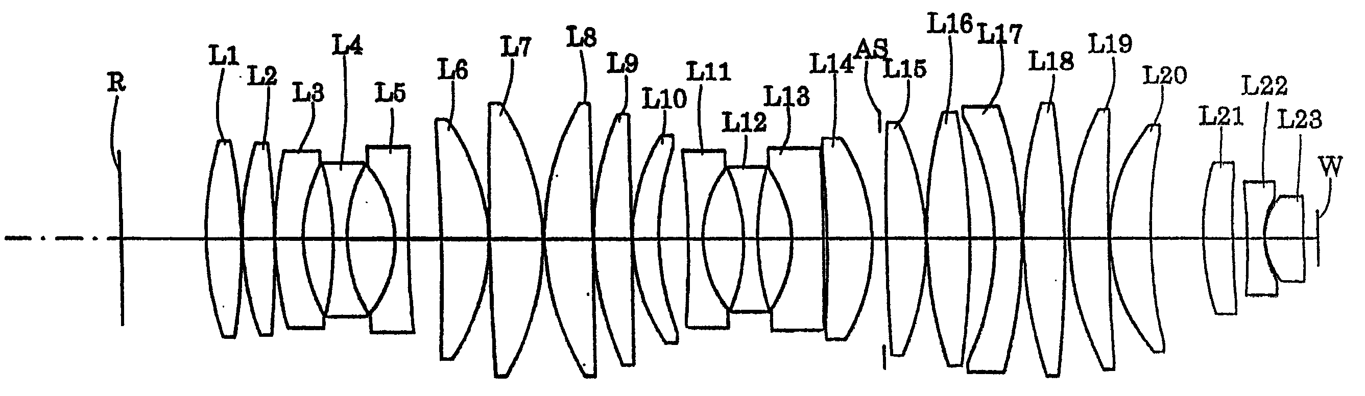
图2所示为关于第一实施例的投影光学系统的透镜构成。参照图2,第一实施例的投影光学系统PL的构成从光罩十字标记侧开始依次为双凸透镜L1、双凸透镜L2、将非球面形状的凹面朝向晶片侧的负凹凸透镜L3、双凹透镜L4、双凹透镜L5、将凹面朝向光罩十字标记侧的正凹凸透镜L6、双凸透镜L7、将平面朝向晶片侧的平凸透镜L8、将平面朝向晶片侧的平凸透镜L9、将非球面形的凹面朝向晶片侧的正凹凸透镜L10、双凹透镜L11、将非球面形状的凹面朝向晶片侧的双凹透镜L12、将凹面朝向光罩十字标记侧的负凹凸透镜L13、将凹面朝向光罩十字标记侧的正凹凸透镜L14、孔径光圈AS、双凸透镜L15、双凸透镜L16、将凹面朝向光罩十字标记侧的负凹凸透镜L17、双凸透镜L18、将凸面朝向光罩十字标记侧的正凹凸透镜L19、将凸面朝向光罩十字标记侧的正凹凸透镜L20、将非球面形状的凹面朝向晶片侧的正凹凸透镜L21、双凹透镜L22、将凸面朝向光罩十字标记侧的正凹凸透镜L23。FIG. 2 shows the lens configuration of the projection optical system related to the first embodiment. Referring to FIG. 2 , the configuration of the projection optical system PL of the first embodiment is a biconvex lens L1, a biconvex lens L2, a negative meniscus lens L3 with an aspherical concave surface facing the wafer side, and a biconcave lens L4 in order from the reticle cross mark side. , biconcave lens L5, positive meniscus lens L6 with the concave surface facing the cross mark side of the mask, biconvex lens L7, plano-convex lens L8 with the plane facing the wafer side, plano-convex lens L9 with the plane facing the wafer side, and an aspheric concave surface facing Positive meniscus lens L10 on the wafer side, biconcave lens L11, biconcave lens L12 with the aspherical concave surface facing the wafer side, negative meniscus lens L13 with the concave surface facing the reticle cross mark side, positive meniscus lens with the concave surface facing the reticle cross mark side Meniscus lens L14, aperture diaphragm AS, biconvex lens L15, biconvex lens L16, negative meniscus lens L17 with the concave surface facing the reticle cross mark side, biconvex lens L18, positive meniscus lens L19 with the convex surface facing the reticle cross mark side, Positive meniscus lens L20 facing the reticle cross mark side, positive meniscus lens L21 with the aspherical concave surface facing the wafer side, biconcave lens L22, and positive meniscus lens L23 with the convex surface facing the reticle cross mark side.
在以下的表(1)中,列举了关于第一实施例的投影光学系统的诸元的值。在表(1)的主要诸元中,分别以λ表示曝光光的中心波长,β表示投影倍率,NA表示像侧(晶片侧)数值孔径,Y0表示最大像高(成像区域半径)。而且,在表(1)的光学构件诸元中,分别以面号码表示从光罩十字标记侧开始的面的顺序,r为各面的曲率半径(在非球面的场合为顶点曲率半径:mm),d为各面的轴上间隔即面间隔(mm),n为对曝光光的中心波长的折射率。上述的表记在以后的表(2)~(6)中也是同样的。In Table (1) below, values of elements of the projection optical system related to the first embodiment are listed. Among the main elements in Table (1), λ represents the central wavelength of the exposure light, β represents the projection magnification, NA represents the numerical aperture of the image side (wafer side), and Y 0 represents the maximum image height (radius of the imaging area). In addition, among the optical components in Table (1), the order of the surfaces from the cross mark side of the mask is indicated by the surface numbers, and r is the radius of curvature of each surface (in the case of an aspheric surface, the radius of curvature of the vertex: mm ), d is the on-axis spacing of each surface, that is, the surface spacing (mm), and n is the refractive index for the central wavelength of the exposure light. The above notation is also the same in the following Tables (2) to (6).
[表1][Table 1]
(主要诸元)(main elements)
λ=248.4nmλ=248.4nm
β=-1/4β=-1/4
NA=0.63NA=0.63
Y0=21.1mmY 0 =21.1mm
(光学部件诸元)(Optical components)
面号码 r d nnoodle number r n
(光罩十字标记面) 85.356(Reticle cross mark side) 85.356
1 336.044 37.114 1.50839(L1)1 336.044 37.114 1.50839(L1)
2 -615.588 12 -615.588 1
3 316.94 33.74 1.50839(L2)3 316.94 33.74 1.50839(L2)
4 -989.58 14 -989.58 1
5 359.629 30.296 1.50839(L3)5 359.629 30.296 1.50839(L3)
6* 159.197 30.8386 * 159.197 30.838
7 83.6739 21.7064 1.50839 (L4)7 83.6739 21.7064 1.50839 (L4)
8 -156.559 49.4888 -156.559 49.488
9 -124.689 15 1.50839 (L5)9 -124.689 15 1.50839 (L5)
10 1160.675 36.00710 1160.675 36.007
11 -2954.927 51.128 1.50839 (L6)11 -2954.927 51.128 1.50839 (L6)
12 -209.121 112 -209.121 1
13 2955.769 55.617 1.50839 (L7)13 2955.769 55.617 1.50839 (L7)
14 -271.245 1.90614 -271.245 1.906
15 274.463 51.753 1.50839 (L8)15 274.463 51.753 1.50839 (L8)
16 ∞ 116 ∞ 1
17 324.91 40.148 1.50839 (L9)17 324.91 40.148 1.50839 (L9)
18 ∞ 118 ∞ 1
19 195.148 28.434 1.50839(L10)19 195.148 28.434 1.50839(L10)
20* 274.486 31.2820 * 274.486 31.28
21 -989.419 15 1.50839(L11)21 -989.419 15 1.50839(L11)
22 117.522 43.7822 117.522 43.78
23 -183.081 15 1.50839(L12)23 -183.081 15 1.50839(L12)
24* 257.814 36.09724 * 257.814 36.097
25 -136.607 33.693 1.50839(L13)25 -136.607 33.693 1.50839(L13)
26 -3057.785 3.80226 -3057.785 3.802
27 -1540.038 47.077 1.50839(L14)27 -1540.038 47.077 1.50839(L14)
28 -207.905 10.53928 -207.905 10.539
29 ∞ 4.66 (AS)29 ∞ 4.66 (AS)
30* 2195.041 42.729 1.50839(L15)30 * 2195.041 42.729 1.50839(L15)
31 -290.604 131 -290.604 1
32 488.043 44.596 1.50839(L16)32 488.043 44.596 1.50839(L16)
33 -776.102 26.23433 -776.102 26.234
34 -290.901 27.5 1.50839(L17)34 -290.901 27.5 1.50839(L17)
35 -487.976 1.91935 -487.976 1.919
36 478.702 42.713 1.50839(L18)36 478.702 42.713 1.50839(L18)
37 -1180.716 4.28337 -1180.716 4.283
38 295.558 41.897 1.50839(L19)38 295.558 41.897 1.50839(L19)
39 2379.702 1.72739 2379.702 1.727
40 191.779 40.82 1.50839(L20)40 191.779 40.82 1.50839(L20)
41 501.27 52.6341 501.27 52.63
42 271.114 29.675 1.50839(L21)42 271.114 29.675 1.50839(L21)
43* 966.299 14.70743 * 966.299 14.707
44 -1253.623 16.248 1.50839(L22)44 -1253.623 16.248 1.50839(L22)
45 87.496 145 87.496 1
46 70.339 39.582 1.50839(L23)46 70.339 39.582 1.50839(L23)
47 616.178 12.980347 616.178 12.9803
(晶片面)(wafer side)
(非球面资料)(Aspherical data)
6面6 sides
κ=0kappa=0
C4=-3.2030×10⁻⁸ C6=-1.3280×10⁻¹² C 4 =-3.2030×10 -8 C 6 =-1.3280×10 -12
C8=-5.4530×10⁻¹⁷ C10=1.8350×10⁻²¹ C 8 =-5.4530×10 -17 C 10 =1.8350×10 -21
C12=-4.4290×10⁻²⁵ C14=1.2610×10⁻²⁹ C 12 =-4.4290×10 -25 C 14 =1.2610×10 -29
20面20 sides
κ=0kappa=0
C4=-7.2400×10⁻⁹ C6=1.6610×10⁻¹⁴ C 4 =-7.2400×10 -9 C 6 =1.6610×10 -14
C8=2.3820×10⁻¹⁸ C10=-6.9760×10⁻²³ C 8 =2.3820×10 -18 C 10 =-6.9760×10 -23
C12=6.6230×10⁻²⁷ C 12 =6.6230×10 -27
24面24 sides
κ=0kappa=0
C4=4.2380×10⁻⁸ C6=-2.3110×10⁻¹² C 4 =4.2380×10 -8 C 6 =-2.3110×10 -12
C8=-2.6420×10⁻¹⁷ C10=4.7740×10⁻²¹ C 8 =-2.6420×10 -17 C 10 =4.7740×10 -21
43面43 sides
κ=0kappa=0
C4=3.6730×10⁻⁸ C6=4.4570×10⁻¹³ C 4 =3.6730×10 -8 C 6 =4.4570×10 -13
C8=2.7930×10⁻¹⁷ C10=-3.3130×10⁻²¹ C 8 =2.7930×10 -17 C 10 =-3.3130×10 -21
C12=4.1110×10⁻²⁵ C 12 =4.1110×10 -25
(条件式对应值)(Conditional corresponding value)
L=1249.9933mmL=1249.9933mm
E=3220.834mmE=3220.834mm
(1)(λ×L)/(NA×Y0 2)=1.107×10⁻³ (1)(λ×L)/(NA×Y 0 2 )=1.107×10 -3
(2)E/L=2.58(2)E/L=2.58
图3所示为第一实施例的球面像差、象散差及歪曲像差。而且,图4所示为第一实施例的横像差。在各像差图中,分别以NA表示像侧的数值孔径,Y表示像高(mm)。在表示象散差的像差图中,实线表示弧矢像面,虚线表示子午线像面。上述的表记在以后的图6、图7、图9、图10、图12、图13、图15、图16中也都是同样的。由各像差图可知,在第一实施例中,可一面确保NA=0.63的大的数值孔径及Y0=21.1mm的大的最大像高(进而为大的成像区域),一面使含有歪曲像差的诸像差被良好地修正。FIG. 3 shows spherical aberration, astigmatism and distortion of the first embodiment. Also, Fig. 4 shows the lateral aberration of the first embodiment. In each aberration diagram, NA represents the numerical aperture on the image side, and Y represents the image height (mm). In the aberration diagram showing astigmatic difference, the solid line indicates the sagittal image plane, and the dotted line indicates the meridian image plane. The above notation is also the same in FIGS. 6 , 7 , 9 , 10 , 12 , 13 , 15 , and 16 hereinafter. From the aberration diagrams, it can be seen that in the first embodiment, while ensuring a large numerical aperture of NA=0.63 and a large maximum image height of Y 0 =21.1mm (and thus a large imaging area), it is possible to minimize distortions. Aberrations of aberrations are well corrected.
[第二实施例][Second embodiment]
图5所示为关于第二实施例的投影光学系统的透镜构成。参照图5,第二实施例的投影光学系统PL的构成从光罩十字标记侧开始依次为双凸透镜L1、双凸透镜L2、将非球面形状的凹面朝向晶片侧的负凹凸透镜L3、双凹透镜L4、将非球面形状的凹面朝向晶片侧的双凹透镜L5、将凹面朝向光罩十字标记侧的负凹凸透镜L6、将凹面朝向光罩十字标记侧的正凹凸透镜L7、将凹面朝向光罩十字标记侧的正凹凸透镜L8、双凸透镜L9、将凸面朝向光罩十字标记侧的正凹凸透镜L10、将非球面形状的凹面朝向晶片侧的双凹透镜L11、将非球面形状的凹面朝向晶片侧的双凹透镜L12、将凹面朝向光罩十字标记侧的负凹凸透镜L13、将非球面形状的凹面朝向光罩十字标记侧的正凹凸透镜L14、孔径光圈AS、双凸透镜L15、双凸透镜L16、将凹面朝向光罩十字标记侧的负凹凸透镜L17、将凸面朝向光罩十字标记侧的正凹凸透镜L18、将凸面朝向光罩十字标记侧的正凹凸透镜L19、将凸面朝向光罩十字标记侧的正凹凸透镜L20、将非球面形状的凹面朝向晶片侧的正凹凸透镜L21、将凸面朝向光罩十字标记侧的负凹凸透镜L22、将凸面朝向光罩十字标记侧的正凹凸透镜L23。FIG. 5 shows the lens configuration of the projection optical system related to the second embodiment. Referring to FIG. 5 , the configuration of the projection optical system PL of the second embodiment is a biconvex lens L1, a biconvex lens L2, a negative meniscus lens L3 with an aspherical concave surface facing the wafer side, and a biconcave lens L4 in order from the reticle cross mark side. , Biconcave lens L5 with aspherical concave surface facing the wafer side, negative meniscus lens L6 with concave surface facing the reticle cross mark side, positive meniscus lens L7 with concave surface facing the reticle cross mark side, concavity face toward the reticle cross mark side Positive meniscus lens L8 on the side, biconvex lens L9, positive meniscus lens L10 with the convex surface facing the reticle cross mark side, biconvex lens L11 with the aspherical concave surface facing the wafer side, biconvex lens with the aspheric concave surface facing the wafer side Concave lens L12, negative meniscus lens L13 with the concave surface facing the reticle cross mark side, positive meniscus lens L14 with the aspherical concave surface Negative meniscus lens L17 on the reticle cross mark side, positive meniscus lens L18 on the reticle cross mark side, positive meniscus lens L19 on the reticle cross mark side, positive lenticular lens on the reticle cross mark side Lens L20, a positive meniscus lens L21 with an aspherical concave surface facing the wafer side, a negative meniscus lens L22 with a convex surface facing the reticle cross mark side, and a positive meniscus lens L23 with a convex surface facing the reticle cross mark side.
在以下的表(2)中,列举了关于第二实施例的投影光学系统的诸元的值。In Table (2) below, values of elements of the projection optical system related to the second embodiment are listed.
[表2][Table 2]
(主要诸元)(main elements)
λ=248.4nmλ=248.4nm
β=-1/4β=-1/4
NA=0.65NA=0.65
Y0=21.1mmY 0 =21.1mm
(光学部件诸元)(Optical components)
面号码 r d nnoodle number r d d n
(光罩十字标记面) 85.000(Reticle cross mark side) 85.000
1 370.169 36.976 1.50839(L1)1 370.169 36.976 1.50839(L1)
2 -539.027 12 -539.027 1
3 260.614 35.323 1.50839(L2)3 260.614 35.323 1.50839(L2)
4 -1805.662 14 -1805.662 1
5 237.342 21.572 1.50839(L3)5 237.342 21.572 1.50839(L3)
6* 139.323 31.3776 * 139.323 31.377
7 -516.888 17 1.50839(L4)7 -516.888 17 1.50839(L4)
8 150 42.4258 150 42.425
9 -147.29 15 1.50839(L5)9 -147.29 15 1.50839(L5)
10* 816.066 35.90510 * 816.066 35.905
11 -147.082 27 1.50839(L6)11 -147.082 27 1.50839(L6)
12 -225.4 112 -225.4 1
13 -41392 53.976 1.50839(L7)13 -41392 53.976 1.50839(L7)
14 -227.618 114 -227.618 1
15 -8068.53 50.952 1.50839(L8)15 -8068.53 50.952 1.50839(L8)
16 -284.185 116 -284.185 1
17 243.06 59.2 1.50839(L9)17 243.06 59.2 1.50839(L9)
18 -37613.5 118 -37613.5 1
19 203.88 49.991 1.50839(L10)19 203.88 49.991 1.50839(L10)
20 1553.442 32.5520 1553.442 32.55
21 -1036.807 17 1.50839(L11)21 -1036.807 17 1.50839(L11)
22* 148.605 42.59422 * 148.605 42.594
23 -191.614 15 1.50839(L12)23 -191.614 15 1.50839(L12)
24* 189.595 41.62524 * 189.595 41.625
25 -146.676 18.454 1.50839(L13)25 -146.676 18.454 1.50839(L13)
26 -1600.717 18.65126 -1600.717 18.651
27* -759.531 35.576 1.50839(L14)27 * -759.531 35.576 1.50839(L14)
28 -211.058 10.00128 -211.058 10.001
29 ∞ 7.194 (AS)29 ∞ 7.194 (AS)
30* 2974.88 48.903 1.50839(L15)30 * 2974.88 48.903 1.50839(L15)
31 -260.354 131 -260.354 1
32 533.226 51.054 1.50839(L16)32 533.226 51.054 1.50839(L16)
33 -497.281 16.33433 -497.281 16.334
34 -297.478 28 1.50839(L17)34 -297.478 28 1.50839(L17)
35 -410.191 6.96235 -410.191 6.962
36 432.489 35.698 1.50839(L18)36 432.489 35.698 1.50839(L18)
37 5542.28 137 5542.28 1
38 339.32 38.398 1.50839(L19)38 339.32 38.398 1.50839(L19)
39 2529.767 1.07339 2529.767 1.073
40 205.053 40.997 1.50839(L20)40 205.053 40.997 1.50839(L20)
41 570.26 44.01641 570.26 44.016
42 526.794 28.369 1.50839(L21)42 526.794 28.369 1.50839(L21)
43* 999.637 7.31643 * 999.637 7.316
44 363.9 26.929 1.50839(L22)44 363.9 26.929 1.50839(L22)
45 80.011 6.36845 80.011 6.368
46 68.127 47.548 1.50839(L23)46 68.127 47.548 1.50839(L23)
47 333.792 13.693347 333.792 13.6933
(晶片面)(wafer side)
(非球面资料)(Aspherical data)
6面6 sides
κ=0kappa=0
C4=-2.5830×10⁻⁸ C6=-1.4132×10⁻¹² C 4 =-2.5830×10 -8 C 6 =-1.4132×10 -12
C8=-7.1032×10⁻¹⁷ C10=9.7808×10⁻²² C 8 =-7.1032×10 -17 C 10 =9.7808×10 -22
C12=-3.4814×10⁻²⁵ C 12 =-3.4814×10 -25
10面10 sides
κ=0kappa=0
C4=-5.2948×10⁻⁹ C6=1.6031×10⁻¹² C 4 =-5.2948×10 -9 C 6 =1.6031×10 -12
C8=-4.1130×10⁻¹⁷ C10=-5.8947×10⁻²² C 8 =-4.1130×10 -17 C 10 =-5.8947×10 -22
C12=3.0968×10⁻²⁶ C 12 =3.0968×10 -26
22面22 sides
κ=0kappa=0
C4=3.2206×10⁻⁸ C6=1.8939×10⁻¹² C 4 =3.2206×10 -8 C 6 =1.8939×10 -12
C8=9.9966×10⁻¹⁷ C10=2.8187×10⁻²¹ C 8 =9.9966×10 -17 C 10 =2.8187×10 -21
C12=4.7609×10⁻²⁵ C 12 =4.7609×10 -25
24面24 sides
κ=0kappa=0
C4=3.8141×10⁻⁸ C6=-3.4162×10⁻¹² C 4 =3.8141×10 -8 C 6 =-3.4162×10 -12
C8=1.2024×10⁻¹⁹ C10=9.9690×10⁻²¹ C 8 =1.2024×10 -19 C 10 =9.9690×10 -21
C12=-2.2108×10⁻²⁵ C 12 =-2.2108×10 -25
27面27 sides
κ=0kappa=0
C4=1.2927×10⁻⁹ C6=1.7523×10⁻¹³ C 4 =1.2927×10 -9 C 6 =1.7523×10 -13
C8=3.6435×10⁻¹⁸ C10=1.1104×10⁻²² C 8 =3.6435×10 -18 C 10 =1.1104×10 -22
C12=1.0330×10⁻²⁶ C 12 =1.0330×10 -26
43面43 sides
κ=0kappa=0
C4=2.3875×10⁻⁸ C6=1.3965×10⁻¹² C 4 =2.3875×10 -8 C 6 =1.3965×10 -12
C8=-4.3074×10⁻¹⁷ C10=3.1012×10⁻²¹ C 8 =-4.3074×10 -17 C 10 =3.1012×10 -21
C12=-1.9832×10⁻²⁶ C 12 =-1.9832×10 -26
(条件式对应值)(Conditional corresponding value)
L=1250.0003mmL=1250.0003mm
E=2913.034mmE=2913.034mm
(1)(λ×L)/(NA×Y0 2)=1.073×10⁻³ (1)(λ×L)/(NA×Y 0 2 )=1.073×10 -3
(2)E/L=2.33(2)E/L=2.33
图6所示为第二实施例的球面像差、象散差及歪曲像差。而且,图7所示为第二实施例的横像差。由各像差图可知,在第二实施例中,可一面确保NA=0.63的大的数值孔径及Y0=21.1mm的大的最大像高(进而为大的成像区域),一面使含有歪曲像差的诸像差被良好地修正。FIG. 6 shows the spherical aberration, astigmatism and distortion of the second embodiment. Also, Fig. 7 shows lateral aberrations of the second embodiment. From the aberration diagrams, it can be seen that in the second embodiment, while ensuring a large numerical aperture of NA=0.63 and a large maximum image height of Y 0 =21.1mm (and thus a large imaging area), it is possible to minimize distortions. Aberrations of aberrations are well corrected.
[第三实施例][Third embodiment]
图8所示为关于第三实施例的投影光学系统的透镜构成。参照图8,第三实施例的投影光学系统PL的构成从光罩十字标记侧开始依次为将凸面朝向光罩十字标记侧的负凹凸透镜L1、将非球面形状的凹面朝向光罩十字标记侧的双凹透镜L2、将凹面朝向光罩十字标记侧的正凹凸透镜L3、将凹面朝向光罩十字标记侧的正凹凸透镜L4、将凸面朝向光罩十字标记侧的正凹凸透镜L5、双凸透镜L6、双凸透镜L7、将非球面形状的凹面朝向晶片侧的负凹凸透镜L8、将非球面形状的凹面朝向晶片侧的负凹凸透镜L9、将非球面形状的凹面朝向晶片侧的双凹透镜L10、双凹透镜L11、将凹面朝向光罩十字标记侧的正凹凸透镜L12、将凹面朝向光罩十字标记侧的正凹凸透镜L13、双凸透镜L14、将凸面朝向光罩十字标记侧的正凹凸透镜L15、孔径光圈AS、将凸面朝向光罩十字标记侧的正凹凸透镜L16、将凸面朝向光罩十字标记侧的正凹凸透镜L17、将凸面朝向光罩十字标记侧的正凹凸透镜L18、将凸面朝向光罩十字标记侧的正凹凸透镜L19、将非球面形状的凹面朝向晶片侧的平凹透镜L20、将非球面形状的凹面朝向晶片侧的负凹凸透镜L21、将凸面朝向光罩十字标记侧的正凹凸透镜L22。FIG. 8 shows the lens configuration of the projection optical system related to the third embodiment. Referring to FIG. 8 , the configuration of the projection optical system PL of the third embodiment is a negative meniscus lens L1 with a convex surface facing the reticle cross mark side, and an aspheric concave surface facing the reticle cross mark side in order from the reticle cross mark side. biconcave lens L2, positive meniscus lens L3 with the concave surface facing the reticle cross mark side, positive meniscus lens L4 with the concave surface facing the reticle cross mark side, positive meniscus lens L5 with the convex surface facing the reticle cross mark side, biconvex lens L6 , biconvex lens L7, negative meniscus lens L8 with an aspherical concave surface facing the wafer side, negative meniscus lens L9 with an aspherical concave surface facing the wafer side, biconcave lens L10 with an aspherical concave surface facing the wafer side, double Concave lens L11, positive meniscus lens L12 with the concave surface facing the reticle cross mark side, positive meniscus lens L13 with the concave surface facing the reticle cross mark side, biconvex lens L14, positive meniscus lens L15 with the convex surface facing the reticle cross mark side, aperture Aperture AS, Positive meniscus lens L16 with the convex surface facing the reticle cross mark side, Positive meniscus lens L17 with the convex surface facing the reticle cross mark side, Positive meniscus lens L18 with the convex surface facing the reticle cross mark side, Convex surface facing the reticle Positive meniscus lens L19 on the cross mark side, plano-concave lens L20 with the aspherical concave surface facing the wafer side, negative meniscus lens L21 with the aspherical concave surface facing the wafer side, positive meniscus lens with the convex surface facing the reticle cross mark side L22.
在以下的表(3)中,列举了关于第三实施例的投影光学系统的诸元的值。另外,在表(3)的主要诸元中,H0为最大物体高,在表(3)的光学构件诸元中,φ为各面的有效半径(mm)。In Table (3) below, values of elements of the projection optical system related to the third embodiment are listed. In addition, among the main elements in Table (3), H 0 is the maximum object height, and among the elements of optical components in Table (3), φ is the effective radius (mm) of each surface.
[表3][table 3]
(主要诸元)(main elements)
λ=248.4nmλ=248.4nm
β=-1/4β=-1/4
NA=0.65NA=0.65
Y0=21.1mmY 0 =21.1mm
H0=84.4mmH 0 =84.4mm
(光学部件诸元)(Optical components)
面号码 r d n φNoodle number r d d n n φ
(光罩十字标记面) 75.474(Reticle cross mark side) 75.474
1 231.822 38.045 1.50839 101.520 (L1)1 231.822 38.045 1.50839 101.520 (L1)
2* 199.861 47.864 99.4552 * 199.861 47.864 99.455
3* -374.56 14 1.50839 100.413 (L2)3 * -374.56 14 1.50839 100.413 (L2)
4 1087.945 57.682 109.7534 1087.945 57.682 109.753
5 -3912.276 42.876 1.50839 132.707 (L3)5 -3912.276 42.876 1.50839 132.707 (L3)
6 -277.623 1 135.6476 -277.623 1 135.647
7 -975.662 34.107 1.50839 140.410 (L4)7 -975.662 34.107 1.50839 140.410 (L4)
8 -310 4.545 142.0688 -310 4.545 142.068
9 460.296 31.573 1.50839 142.104 (L5)9 460.296 31.573 1.50839 142.104 (L5)
10 13824.8 1 141.04710 13824.8 1 141.047
11 345.841 39.937 1.50839 136.553 (L6)11 345.841 39.937 1.50839 136.553 (L6)
12 -4264.05 1 134.15412 -4264.05 1 134.154
13 256.582 42.585 1.50839 120.583 (L7)13 256.582 42.585 1.50839 120.583 (L7)
14 -2435.28 1 116.22214 -2435.28 1 116.222
15 557.373 14 1.50839 104.606 (L8)15 557.373 14 1.50839 104.606 (L8)
16* 157.296 15.308 85.85916 * 157.296 15.308 85.859
17 246.555 33.989 1.50839 84.985 (L9)17 246.555 33.989 1.50839 84.985 (L9)
18* 111.492 37.164 68.31918 * 111.492 37.164 68.319
19 -155.285 14 1.50839 67.684 (L10)19 -155.285 14 1.50839 67.684 (L10)
20* 158.037 45.453 65.47920 * 158.037 45.453 65.479
21 -90.143 14.012 1.50839 65.860 (L11)21 -90.143 14.012 1.50839 65.860 (L11)
22 1112.61 37.578 86.11722 1112.61 37.578 86.117
23 -641.094 41.361 1.50839 107.984 (L12)23 -641.094 41.361 1.50839 107.984 (L12)
24 -178.026 1 113.52124 -178.026 1 113.521
25 -1135.282 38.98 1.50839 129.498 (L13)25 -1135.282 38.98 1.50839 129.498 (L13)
26 -257.706 1 132.71926 -257.706 1 132.719
27 4389.8 38.124 1.50839 141.281(L14)27 4389.8 38.124 1.50839 141.281(L14)
28 -399.252 1 142.50828 -399.252 1 142.508
29 349.711 27.065 1.50839 142.696(L15)29 349.711 27.065 1.50839 142.696(L15)
30 683.493 70.062 141.25130 683.493 70.062 141.251
31 ∞ 107.614 138.646(AS)31 ∞ 107.614 138.646(AS)
32 441.733 30 1.50839 142.714(L16)32 441.733 30 1.50839 142.714(L16)
33 3010.506 1 141.92433 3010.506 1 141.924
34 259.936 35.745 1.50839 138.201(L17)34 259.936 35.745 1.50839 138.201(L17)
35 683.423 1 135.64935 683.423 1 135.649
36 220.377 33.003 1.50839 127.270(L18)36 220.377 33.003 1.50839 127.270(L18)
37 452.009 1 123.15737 452.009 1 123.157
38 177.601 39.097 1.50839 111.415(L19)38 177.601 39.097 1.50839 111.415(L19)
39 575.408 20.306 105.67039 575.408 20.306 105.670
40 ∞ 16 1.50839 96.125(L20)40 ∞ 16 1.50839 96.125(L20)
1* 844.277 40.65 85.6701 * 844.277 40.65 85.670
42 1622.9 14 1.50839 58.186(L21)42 1622.9 14 1.50839 58.186(L21)
43* 134.25 1 48.30843 * 134.25 1 48.308
44 71.19 29.261 1.50839 4.506(L22)44 71.19 29.261 1.50839 4.506(L22)
45 232.287 17.5256 34.91145 232.287 17.5256 34.911
(晶片面)(wafer side)
(非球面资料)(Aspherical data)
2面2 sides
κ=0kappa=0
C4=-4.1502×10⁻⁸ C6=2.9831×10⁻¹³ C 4 =-4.1502×10 -8 C 6 =2.9831×10 -13
C8=2.2965×10⁻¹⁷ C10=-3.3074×10⁻²¹ C 8 =2.2965×10 -17 C 10 =-3.3074×10 -21
C12=3.0534×10⁻²⁵ C14=-1.5922×10⁻²⁹ C 12 =3.0534×10 -25 C 14 =-1.5922×10 -29
C16=2.5895×10⁻³⁴ C 16 =2.5895×10 -34
3面3 sides
κ=0kappa=0
C4=-4.1155×10⁻⁸ C6=-4.2875×10⁻¹³ C 4 =-4.1155×10 -8 C 6 =-4.2875×10 -13
C8=1.1750×10⁻¹⁷ C10=4.8956×10⁻²² C 8 =1.1750×10 -17 C 10 =4.8956×10 -22
C12=-2.2368×10⁻²⁵ C14=2.0569×10⁻²⁹ C 12 =-2.2368×10 -25 C 14 =2.0569×10 -29
C16=-8.3869×10⁻³⁴ C 16 =-8.3869×10 -34
16面16 sides
κ=0kappa=0
C4=4.4486×10⁻⁸ C6=-2.9141×10⁻¹⁵ C 4 =4.4486×10 -8 C 6 =-2.9141×10 -15
C8=1.2928×10⁻¹⁶ C10=5.2310×10⁻²¹ C 8 =1.2928×10 -16 C 10 =5.2310×10 -21
C12=2.7283×10⁻²⁵ C14=5.4172×10⁻²⁹ C 12 =2.7283×10 -25 C 14 =5.4172×10 -29
C16=5.5839×10⁻³⁴ C 16 =5.5839×10 -34
18面18 sides
κ=0kappa=0
C4=-1.3891×10⁻⁷ C6=-3.0973×10⁻¹³ C 4 =-1.3891×10 -7 C 6 =-3.0973×10 -13
C8=-3.9700×10⁻¹⁶ C10=-7.9024×10⁻²⁰ C 8 =-3.9700×10 -16 C 10 =-7.9024×10 -20
C12=7.8062×10⁻²⁴ C14=-3.0617×10⁻²² C 12 =7.8062×10 -24 C 14 =-3.0617×10 -22
C16=2.0719×10⁻³¹ C 16 =2.0719×10 -31
20面20 sides
κ=0kappa=0
C4=4.8876×10⁻⁸ C6=-6.8085×10⁻¹² C 4 =4.8876×10 -8 C 6 =-6.8085×10 -12
C8=5.9452×10⁻¹⁶ C10=1.7262×10⁻²⁰ C 8 =5.9452×10 -16 C 10 =1.7262×10 -20
C12=8.4920×10⁻²⁴ C14=-1.3744×10⁻²⁷ C 12 =8.4920×10 -24 C 14 =-1.3744×10 -27
C12=8.9638×10⁻³² C 12 =8.9638×10 -32
41面41 sides
κ=0kappa=0
C4=1.1607×10⁻⁸ C6=4.3405×10⁻¹³ C 4 =1.1607×10 -8 C 6 =4.3405×10 -13
C8=-8.0755×10⁻¹⁷ C10=6.3294×10⁻²¹ C 8 =-8.0755×10 -17 C 10 =6.3294×10 -21
C12=-3.8914×10⁻²⁵ C14=2.0077×10⁻²⁹ C 12 =-3.8914×10 -25 C 14 =2.0077×10 -29
C16=-5.3721×10⁻³⁴ C 16 =-5.3721×10 -34
43面43 sides
κ=0kappa=0
C4=3.3236×10⁻⁸ C6=-1.4246×10⁻¹¹ C 4 =3.3236×10 -8 C 6 =-1.4246×10 -11
C8=-1.2965×10⁻¹⁵ C10=-2.1005×10⁻¹⁹ C 8 =-1.2965×10 -15 C 10 =-2.1005×10 -19
C12=5.6985×10⁻²⁴ C14=4.4185×10⁻²⁷ C 12 =5.6985×10 -24 C 14 =4.4185×10 -27
C16=-1.6556×10⁻³¹ C 16 =-1.6556×10 -31
(条件式对应值)(Conditional corresponding value)
L=1249.9856mmL=1249.9856mm
E=1644.276mmE=1644.276mm
(1)(λ×L)/(NA×Y0 2)=1.026×10⁻³ (1)(λ×L)/(NA×Y 0 2 )=1.026×10 -3
(2)E/L=1.32(2)E/L=1.32
图9所示为第三实施例的球面像差、象散差及歪曲像差。而且,图10所示为第三实施例的横像差。由各像差图可知,在第三实施例中,可一面确保NA=0.63的大的数值孔径及Y0=21.1mm的大的最大像高(进而为大的成像区域),一面使含有歪曲像差的诸像差被良好地修正。FIG. 9 shows spherical aberration, astigmatism and distortion of the third embodiment. Also, Fig. 10 shows the lateral aberration of the third embodiment. From the aberration diagrams, it can be seen that in the third embodiment, while ensuring a large numerical aperture of NA=0.63 and a large maximum image height of Y 0 =21.1mm (and thus a large imaging area), it is possible to minimize distortions. Aberrations of aberrations are well corrected.
如上所述,关于第一实施例~第三实施例的投影光学系统PL,由具有1.6以下的折射率的光学材料而形成,在物体侧及像侧两处为实质上的远心,满足(λ×L)/(NA×Y0 2)<1.5×10⁻³的条件,所以能够一面确保足够大的数值孔径及足够宽广的成像区域,一面使含有失真的诸像差被良好地修正,形成简洁而高性能的光学系统。As described above, the projection optical system PL of the first to third embodiments is formed of an optical material having a refractive index of 1.6 or less, is substantially telecentric at both the object side and the image side, and satisfies ( λ×L)/(NA×Y 0 2 )<1.5×10 -3 , so while ensuring a sufficiently large numerical aperture and a sufficiently wide imaging area, various aberrations including distortion can be well corrected, The result is a compact yet high-performance optical system.
[第四实施例][Fourth embodiment]
图11所示为关于第四实施例的投影光学系统的透镜构成。参照图11,第四实施例之投影光学系统PL的构成从光罩十字标记侧开始依次为双凸透镜L1、双凸透镜L2、将非球面形状的凹面朝向晶片侧的负凹凸透镜L3、将凸面朝向光罩十字标记侧的负凹凸透镜L4、双凹透镜L5、将凹面朝向光罩十字标记侧的负凹凸透镜L6、将非球面形状的凹面朝向光罩十字标记侧的正凹凸透镜L7、将凹面朝向光罩十字标记侧的正凹凸透镜L8、将凹面朝向光罩十字标记侧的正凹凸透镜L9、将凸面朝向光罩十字标记侧的正凹凸透镜L10、将凸面朝向光罩十字标记侧的正凹凸透镜L11、将凸面朝向光罩十字标记侧的负凹凸透镜L12、将非球面形状的凹面朝向光罩十字标记侧的双凹透镜L13、将非球面形状的凹面朝向光罩十字标记侧的双凹透镜L14、将凹面朝向光罩十字标记侧的负凹凸透镜L15、将非球面形状的凹面朝向光罩十字标记侧的正凹凸透镜L16、孔径光圈AS、将凹面朝向光罩十字标记侧的正凹凸透镜L17、双凸透镜L18、将凹面朝向光罩十字标记侧的负凹凸透镜L19、双凸透镜L20、将非球面形状的凹面朝向晶片侧的正凹凸透镜L21、将凸面朝向光罩十字标记侧的负凹凸透镜L22、将凸面朝向光罩十字标记侧的负凹凸透镜L23、将凸面朝向光罩十字标记侧的负凹凸透镜L24、将凸面朝向光罩十字标记侧的正凹凸透镜L25。FIG. 11 shows the lens configuration of the projection optical system related to the fourth embodiment. Referring to FIG. 11 , the configuration of the projection optical system PL of the fourth embodiment is a biconvex lens L1, a biconvex lens L2, a negative meniscus lens L3 with the aspherical concave surface facing the wafer side, and a convex surface facing Negative meniscus lens L4 on the reticle cross mark side, double concave lens L5, negative meniscus lens L6 with the concave surface facing the reticle cross mark side, positive meniscus lens L7 with the aspherical concave surface facing the reticle cross mark side, and Positive meniscus lens L8 on the reticle cross mark side, positive meniscus lens L9 with the concave surface facing the reticle cross mark side, positive meniscus lens L10 with the convex surface facing the reticle cross mark side, positive meniscus lens with the convex surface facing the reticle cross mark side Lens L11, negative meniscus lens L12 with a convex surface facing the reticle cross mark side, biconcave lens L13 with an aspherical concave surface facing the reticle cross mark side, biconcave lens L14 with an aspherical concave surface facing the reticle cross mark side , Negative meniscus lens L15 with the concave surface facing the reticle cross mark side, positive meniscus lens L16 with the aspherical concave surface facing the reticle cross mark side, aperture stop AS, positive meniscus lens L17 with the concave surface facing the reticle cross mark side , lenticular lens L18, negative meniscus lens L19 with the concave surface facing the cross mark side of the reticle, lenticular lens L20, positive meniscus lens L21 with the aspherical concave surface facing the wafer side, negative meniscus lens with the convex surface facing the cross mark side of the reticle L22, negative meniscus lens L23 whose convex surface faces the reticle cross mark side, negative meniscus lens L24 whose convex surface faces the reticle cross mark side, and positive meniscus lens L25 whose convex surface faces the reticle cross mark side.
在第四实施例中,所有的透镜都由石英形成。在以下的表(4)中,列举了关于第四实施例的投影光学系统的诸元的值。In the fourth embodiment, all lenses are formed of quartz. In Table (4) below, values of elements of the projection optical system related to the fourth embodiment are listed.
[表4][Table 4]
(主要诸元)(main elements)
λ=193.3nmλ=193.3nm
β=-1/4β=-1/4
NA=0.70NA=0.70
Y0=21.1mmY 0 =21.1mm
(光学部件诸元)(Optical components)
面号码 r d nnoodle number r r d n
(光罩十字标记面) 55.977(Reticle cross mark side) 55.977
1 236.375 36.708 1.560326(L1)1 236.375 36.708 1.560326(L1)
2 -1326.857 1.0002 -1326.857 1.000
3 305.858 27.807 1.560326(L2)3 305.858 27.807 1.560326(L2)
4 -4988.919 1.0004 -4988.919 1.000
5 478.298 13.000 1.560326(L3)5 478.298 13.000 1.560326(L3)
6* 216.036 3.8776 * 216.036 3.877
7 246.432 13.000 1.560326(L4)7 246.432 13.000 1.560326(L4)
8 142.617 42.5148 142.617 42.514
9 -176.904 13.000 1.560326(L5)9 -176.904 13.000 1.560326(L5)
10 212.782 47.10210 212.782 47.102
11 -134.266 13.000 1.560326(L6)11 -134.266 13.000 1.560326(L6)
12 -276.220 1.00012 -276.220 1.000
13* -312.207 13.000 1.560326(L7)13 * -312.207 13.000 1.560326(L7)
14 -305.626 13.45314 -305.626 13.453
15 -3214.315 61.536 1.560326(L8)15 -3214.315 61.536 1.560326(L8)
16 -190.911 1.31616 -190.911 1.316
17 -837.247 37.999 1.560326(L9)17 -837.247 37.999 1.560326(L9)
18 -291.832 27.81718 -291.832 27.817
19 266.829 52.664 1.560326(L10)19 266.829 52.664 1.560326(L10)
20 11121.118 1.00020 11121.118 1.000
21 200.702 52.406 1.560326(L11)21 200.702 52.406 1.560326(L11)
22 2260.973 10.96022 2260.973 10.960
23 386.778 13.004 1.560326(L12)23 386.778 13.004 1.560326(L12)
24 152.011 41.78124 152.011 41.781
25* -300.824 13.000 1.560326(L13)25 * -300.824 13.000 1.560326(L13)
26 156.593 35.07026 156.593 35.070
27* -262.372 13.046 1.560326(L14)27 * -262.372 13.046 1.560326(L14)
28 282.691 39.67428 282.691 39.674
29 -152.110 33.875 1.560326(L15)29 -152.110 33.875 1.560326(L15)
30 -205.290 13.00030 -205.290 13.000
31* -946.981 39.169 1.560326(L16)31 * -946.981 39.169 1.560326(L16)
32 -230.012 8.00032 -230.012 8.000
33 ∞ 8.067 (AS)33 ∞ 8.067 (AS)
34 -1744.140 47.891 1.560326(L17)34 -1744.140 47.891 1.560326(L17)
35 -245.859 6.84235 -245.859 6.842
36 445.398 57.580 1.560326(L18)36 445.398 57.580 1.560326(L18)
37 -411.974 13.00037 -411.974 13.000
38 -300.000 27.000 1.560326(L19)38 -300.000 27.000 1.560326(L19)
39 -1310.387 1.03839 -1310.387 1.038
40 629.495 46.394 1.560326(L20)40 629.495 46.394 1.560326(L20)
41 -1301.217 1.13341 -1301.217 1.133
42 300.000 41.497 1.560326(L21)42 300.000 41.497 1.560326(L21)
43* 572.761 1.03243 * 572.761 1.032
44 197.744 36.450 1.560326(L22)44 197.744 36.450 1.560326(L22)
45* 546.586 1.00045 * 546.586 1.000
46 283.437 13.000 1.560326(L23)46 283.437 13.000 1.560326(L23)
47 108.534 20.41147 108.534 20.411
48 177.134 55.444 1.560326(L24)48 177.134 55.444 1.560326(L24)
49 123.882 1.00049 123.882 1.000
50 78.959 67.373 1.560326(L25)50 78.959 67.373 1.560326(L25)
51 482.436 13.09451 482.436 13.094
(晶片面)(wafer side)
(非球面资料)(Aspherical data)
6面6 sides
κ=0kappa=0
C4=-0.390730×10⁻⁷ C6=0.277980×10⁻¹³ C 4 =-0.390730×10 -7 C 6 =0.277980×10 -13
C8=0.448296×10⁻¹⁷ C10=0.142951×10⁻²⁰ C 8 =0.448296×10 -17 C 10 =0.142951×10 -20
C12=-0.200639×10⁻²⁵ C 12 =-0.200639×10 -25
13面13 sides
κ=0kappa=0
C4=-0.234706×10⁻⁷ C6=-0.309208×10⁻¹² C 4 =-0.234706×10 -7 C 6 =-0.309208×10 -12
C8=-0.917319×10⁻¹⁷ C10=-0.195900×10⁻²¹ C 8 =-0.917319×10 -17 C 10 =-0.195900×10 -21
C12=-0.149005×10⁻²⁵ C 12 =-0.149005×10 -25
25面25 sides
κ=0kappa=0
C4=-0.436112×10⁻⁷ C6=0.388626×10⁻¹¹ C 4 =-0.436112×10 -7 C 6 =0.388626×10 -11
C8=-0.127775×10⁻¹⁵ C10=0.347307×10⁻²⁰ C 8 =-0.127775×10 −15 C 10 =0.347307×10 −20
C12=-0.812555×10⁻²⁵ C 12 =-0.812555×10 -25
27面27 sides
κ=0kappa=0
C4=-0.359877×10⁻⁷ C6=-0.413098×10⁻¹¹ C 4 =-0.359877×10 -7 C 6 =-0.413098×10 -11
C8=0.274168×10⁻¹⁶ C10=-0.544566×10⁻²⁰ C 8 =0.274168×10 -16 C 10 =-0.544566×10 -20
C12=-0.351659×10⁻²⁴ C 12 =-0.351659×10 -24
31面31 sides
κ=0kappa=0
C4=-0.781800×10⁻⁸ C6=0.625582×10⁻¹² C 4 =-0.781800×10 -8 C 6 =0.625582×10 -12
C8=-0.767116×10⁻¹⁷ C10=0.242844×10⁻²¹ C 8 =-0.767116×10 −17 C 10 =0.242844×10 −21
C12=-0.585103×10⁻²⁶ C 12 =-0.585103×10 -26
43面43 sides
κ=0kappa=0
C4=-0.480511×10⁻⁸ C6=-0.424626×10⁻¹⁴ C 4 =-0.480511×10 -8 C 6 =-0.424626×10 -14
C8=-0.773379×10⁻¹⁷ C10=-0.156710×10⁻²¹ C 8 =-0.773379×10 -17 C 10 =-0.156710×10 -21
C12=0.781612×10⁻²⁶ C 12 =0.781612×10 -26
45面45 sides
κ=0kappa=0
C4=-0.126619×10⁻⁷ C6=0.111075×10⁻¹¹ C 4 =-0.126619×10 -7 C 6 =0.111075×10 -11
C8=-0.315462×10⁻¹⁷ C10=-0.234952×10⁻²¹ C 8 =-0.315462× 10⁻¹⁷ C 10 =-0.234952×10- 21
C12=0.165000×10⁻²⁵ C 12 =0.165000×10 -25
(条件式对应值)(Conditional corresponding value)
L=1250.00mmL=1250.00mm
(3)(λ×L)/(NA×Y0 2)=0.775×10⁻³ (3) (λ×L)/(NA×Y 0 2 )=0.775×10 -3
图12所示为第四实施例的球面像差、象散差及歪曲像差。而且,图13所示为第四实施例的横像差。由各像差图可知,在第四实施例中,可一面确保NA=0.70的大的数值孔径及Y0=21.1mm的大的最大像高(进而为大的成像区域),一面使含有歪曲像差的诸像差被良好地修正。FIG. 12 shows the spherical aberration, astigmatism and distortion of the fourth embodiment. Also, FIG. 13 shows lateral aberrations of the fourth embodiment. It can be seen from the aberration diagrams that, in the fourth embodiment, while ensuring a large numerical aperture of NA=0.70 and a large maximum image height of Y 0 =21.1mm (and thus a large imaging area), it is possible to minimize distortions. Aberrations of aberrations are well corrected.
[第五实施例][Fifth Embodiment]
图14所示为关于第五实施例的投影光学系统的透镜构成。参照图14,第五实施例的投影光学系统PL的构成从光罩十字标记侧开始依次为双凸透镜L1、双凸透镜L2、将非球面形状的凹面朝向晶片侧的负凹凸透镜L3、将凸面朝向光罩十字标记侧的负凹凸透镜L4、双凹透镜L5、将凹面朝向光罩十字标记侧的负凹凸透镜L6、将非球面形状的凹面朝向光罩十字标记侧的负凹凸透镜L7、将凹面朝向光罩十字标记侧的正凹凸透镜L8、将凹面朝向光罩十字标记侧的正凹凸透镜L9、双凸透镜L10、将凸面朝向光罩十字标记侧的正凹凸透镜L11、将凸面朝向光罩十字标记侧的负凹凸透镜L12、将非球面形状的凹面朝向光罩十字标记侧的双凹透镜L13、将非球面形状的凹面朝向光罩十字标记侧的双凹透镜L14、将凹面朝向光罩十字标记侧的负凹凸透镜L15、将非球面形状的凹面朝向光罩十字标记侧的正凹凸透镜L16、孔径光圈AS、将凹面朝向光罩十字标记侧的正凹凸透镜L17、双凸透镜L18、将凹面朝向光罩十字标记侧的负凹凸透镜L19、将凹面朝向光罩十字标记侧的正凹凸透镜L20、将非球面形状的凹面朝向晶片侧的正凹凸透镜L21、将非球面形状的凹面朝向晶片侧的正凹凸透镜L22、将凸面朝向光罩十字标记侧的负凹凸透镜L23、将凸面朝向光罩十字标记侧的负凹凸透镜L24、将凸面朝向光罩十字标记侧的正凹凸透镜L25。FIG. 14 shows the lens configuration of the projection optical system related to the fifth embodiment. Referring to FIG. 14 , the configuration of the projection optical system PL of the fifth embodiment is a biconvex lens L1, a biconvex lens L2, a negative meniscus lens L3 with the aspherical concave surface facing the wafer side, and a convex surface Negative meniscus lens L4 on the cross mark side of the reticle, double concave lens L5, negative meniscus lens L6 with the concave surface facing the cross mark side of the reticle, negative meniscus lens L7 with the aspherical concave surface facing the cross mark side of the reticle, and Positive meniscus lens L8 on the reticle cross mark side, positive meniscus lens L9 with the concave surface facing the reticle cross mark side, biconvex lens L10, positive meniscus lens L11 with the convex surface facing the reticle cross mark side, and convex surface facing the reticle cross mark side Negative meniscus lens L12 on the side, biconcave lens L13 with the aspherical concave surface facing the reticle cross mark side, biconcave lens L14 with the aspherical concave surface facing the reticle cross mark side, Negative meniscus lens L15, positive meniscus lens L16 with the aspherical concave surface facing the reticle cross mark side, aperture stop AS, positive meniscus lens L17 with the concave surface facing the reticle cross mark side, biconvex lens L18, concavity face toward the reticle Negative meniscus lens L19 on the cross mark side, positive meniscus lens L20 with the concave surface facing the cross mark side of the mask, positive meniscus lens L21 with the aspherical concave surface facing the wafer side, positive meniscus lens L21 with the aspherical concave surface facing the wafer side Lens L22, negative meniscus lens L23 whose convex surface faces the reticle cross mark side, negative meniscus lens L24 whose convex surface faces the reticle cross mark side, and positive meniscus lens L25 whose convex surface faces the reticle cross mark side.
在第五实施例中,透镜L11、L16、L24及L25由萤石形成,其它的透镜由石英形成。在以下的表(5)中,列举了关于第五实施例的投影光学系统的诸元的值。In the fifth embodiment, the lenses L11, L16, L24, and L25 are formed of fluorite, and the other lenses are formed of quartz. In Table (5) below, values of elements of the projection optical system related to the fifth embodiment are listed.
[表5][table 5]
(主要诸元)(main elements)
λ=193.3nmλ=193.3nm
β=-1/4β=-1/4
NA=0.70NA=0.70
Y0=21.1mmY 0 =21.1mm
(光学部件诸元)(Optical components)
面号码 r d nnoodle number r r d d n
(光罩十字标记面) 51.000 (Reticle cross mark side) 51.000
1 213.222 38.539 1.560326(L1)1 213.222 38.539 1.560326(L1)
2 -1490.368 1.0002 -1490.368 1.000
3 438.510 22.960 1.560326(L2)3 438.510 22.960 1.560326(L2)
4 -5521.851 1.0004 -5521.851 1.000
5 333.571 13.000 1.560326(L3)5 333.571 13.000 1.560326(L3)
6* 177.450 4.1616 * 177.450 4.161
7 199.366 13.275 1.560326(L4)7 199.366 13.275 1.560326(L4)
8 138.570 44.6328 138.570 44.632
9 -161.840 13.000 1.560326(L5)9 -161.840 13.000 1.560326(L5)
10 223.766 44.90210 223.766 44.902
11 -143.814 13.000 1.560326(L6)11 -143.814 13.000 1.560326(L6)
12 -298.377 1.70412 -298.377 1.704
3* -334.582 13.000 1.560326(L7)3 * -334.582 13.000 1.560326(L7)
14 -334.916 11.74314 -334.916 11.743
5 -4047.282 57.701 1.560326(L8)5 -4047.282 57.701 1.560326(L8)
16 -201.085 1.00016 -201.085 1.000
17 -1435.546 40.566 1.560326(L9)17 -1435.546 40.566 1.560326(L9)
18 -302.600 21.43818 -302.600 21.438
19 262.122 54.652 1.560326(L10)19 262.122 54.652 1.560326(L10)
20 -11336.582 1.00020 -11336.582 1.000
21 196.075 53.198 1.501455(L11)21 196.075 53.198 1.501455(L11)
22 3379.224 10.47022 3379.224 10.470
23 369.741 13.000 1.560326(L12)23 369.741 13.000 1.560326(L12)
24 153.333 40.35724 153.333 40.357
25* -303.585 13.000 1.560326(L13)25 * -303.585 13.000 1.560326(L13)
26 159.474 35.08926 159.474 35.089
27* -234.626 13.000 1.560326(L14)27 * -234.626 13.000 1.560326(L14)
28 270.159 38.99228 270.159 38.992
29 -165.469 35.787 1.560326(L15)29 -165.469 35.787 1.560326(L15)
30 -196.726 13.00030 -196.726 13.000
31* -735.265 37.631 1.501455(L16)31 * -735.265 37.631 1.501455(L16)
32 -216.484 8.00032 -216.484 8.000
33 ∞ 8.000 (AS)33 ∞ 8.000 (AS)
34 -2040.786 53.321 1.560326(L17)34 -2040.786 53.321 1.560326(L17)
35 -225.458 6.84235 -225.458 6.842
36 552.343 57.580 1.560326(L18)36 552.343 57.580 1.560326(L18)
37 -414.088 13.00037 -414.088 13.000
38 -300.000 27.000 1.560326(L19)38 -300.000 27.000 1.560326(L19)
39 -1036.554 16.15339 -1036.554 16.153
40 -1325.080 46.394 1.560326(L20)40 -1325.080 46.394 1.560326(L20)
41 -376.256 1.00041 -376.256 1.000
42 300.000 41.497 1.560326(L21)42 300.000 41.497 1.560326(L21)
43* 454.030 1.00043 * 454.030 1.000
44 185.557 48.502 1.560326(L22)44 185.557 48.502 1.560326(L22)
45* 970.728 1.20445 * 970.728 1.204
46 374.033 20.165 1.560326(L23)46 374.033 20.165 1.560326(L23)
47 120.058 9.82547 120.058 9.825
48 144.788 48.299 1.501455(L24)48 144.788 48.299 1.501455(L24)
49 100.193 1.00049 100.193 1.000
50 74.978 63.000 1.501455(L25)50 74.978 63.000 1.501455(L25)
51 412.784 11.42251 412.784 11.422
(晶片面)(wafer side)
(非球面资料)(Aspherical data)
6面6 sides
κ=0kappa=0
C4=-0.340666×10⁻⁷ C6=-0.320328×10⁻¹³ C 4 =-0.340666×10 -7 C 6 =-0.320328×10 -13
C8=-0.886363×10⁻¹⁷ C10=0.377243×10⁻²⁰ C 8 =-0.886363×10 −17 C 10 =0.377243×10 −20
C12=-0.403299×10⁻²⁴ C 12 =-0.403299×10 -24
13面13 sides
κ=0kappa=0
C4=-0.115164×10⁻⁷ C6=-0.129368×10⁻¹² C 4 =-0.115164×10 -7 C 6 =-0.129368×10 -12
C8=0.153108×10⁻¹⁷ C10=-0.400820×10⁻²¹ C 8 =0.153108×10 -17 C 10 =-0.400820×10 -21
C12=0.893904×10⁻²⁶ C 12 =0.893904×10 −26
25面25 sides
κ=0kappa=0
C4=-0.610648×10⁻⁷ C6=0.525010×10⁻¹¹ C 4 =-0.610648×10 -7 C 6 =0.525010×10 -11
C8=-0.504609×10⁻¹⁶ C10=-0.696687×10⁻²⁰ C 8 =-0.504609×10 -16 C 10 =-0.696687×10 -20
C12=0.272899×10⁻²⁴ C 12 =0.272899×10 -24
27面27 sides
κ=0kappa=0
C4=-0.558894×10⁻⁷ C6=-0.492800×10⁻¹¹ C 4 =-0.558894×10 -7 C 6 =-0.492800×10 -11
C8=-0.480602×10⁻¹⁶ C10=-0.623444×10⁻²⁰ C 8 =-0.480602×10 -16 C 10 =-0.623444×10 -20
C12=-0.711183×10⁻²⁴ C 12 =-0.711183×10 -24
31面31 sides
κ=0kappa=0
C4=-0.119246×10⁻⁷ C6=0.435184×10⁻¹² C 4 =-0.119246×10 -7 C 6 =0.435184×10 -12
C8=-0.397771×10⁻¹⁷ C10=0.205602×10⁻²¹ C 8 =-0.397771×10 -17 C 10 =0.205602×10 -21
C12=-0.942057×10⁻²⁷ C 12 =-0.942057×10 -27
43面43 sides
κ=0kappa=0
C4=-0.105535×10⁻⁸ C6=-0.924566×10⁻¹³ C 4 =-0.105535×10 -8 C 6 =-0.924566×10 -13
C8=-0.240759×10⁻¹⁷ C10=-0.153687×10⁻²¹ C 8 =-0.240759×10 -17 C 10 =-0.153687×10 -21
C12=0.590155×10⁻²⁶ C 12 =0.590155×10 -26
45面45 sides
κ=0kappa=0
C4=-0.108578×10⁻⁷ C6=0.130055×10⁻¹¹ C 4 =-0.108578×10 -7 C 6 =0.130055×10 -11
C8=-0.312792×10⁻¹⁶ C10=0.526315×10⁻²¹ C 8 =-0.312792×10 -16 C 10 =0.526315×10 -21
C12=-0.463864×10⁻²⁶ C 12 =-0.463864×10 -26
(条件式对应值)(Conditional corresponding value)
L=1250.0mmL=1250.0mm
(3)(λ×L)/(N A×Y0 2)=0.775×10⁻³ (3) (λ×L)/(N A×Y 0 2 )=0.775×10 -3
图15所示为第五实施例的球面像差、象散差及歪曲像差。而且,图16所示为第五实施例的横像差。由各像差图可知,在第五实施例中,可一面确保NA=0.70的大的数值孔径及Y0=21.1mm的大的最大像高(进而为大的成像区域),一面使含有歪曲像差的诸像差被良好地修正。FIG. 15 shows the spherical aberration, astigmatism and distortion of the fifth embodiment. Also, Fig. 16 shows the lateral aberration of the fifth embodiment. From the aberration diagrams, it can be seen that in the fifth embodiment, while ensuring a large numerical aperture of NA=0.70 and a large maximum image height of Y 0 =21.1mm (and thus a large imaging area), it is possible to minimize distortions. Aberrations of aberrations are well corrected.
如上所述,关于第四实施例及第五实施例的投影光学系统PL,由具有1.6以下的折射率的光学材料而形成,在物体侧及像侧两处为实质上的远心,七个光学面形成为非球面形状,满足As described above, the projection optical systems PL of the fourth and fifth embodiments are formed of an optical material having a refractive index of 1.6 or less, two places on the object side and the image side are substantially telecentric, and seven The optical surface is formed into an aspheric shape, satisfying
(λ×L)/(NA×Y0 2)<1.0×10⁻³的条件。The condition of (λ×L)/(NA×Y 0 2 )<1.0×10 -3 .
在第四实施例及第五实施例中,借由满足条件式(3),可一面确保高分辨率及大视野(一面确保足够大的数值孔径及足够宽广的成像区域)一面得到简洁的光学系统,在用于曝光装置的场合可实现高生产量。具体地说,当在条件式(3)的上限值以上时,关于分辨率、成像区域(曝光区域)及光学系统的大小其中的至少一点,不能得到足够优良的构成。另外,为了更加良好地发挥本发明的效果,将条件式(3)的上限值设定成0.9×10⁻³为佳。而且,借由满足条件式(4),可使投影光学系统PL的分辨率提高。In the fourth embodiment and the fifth embodiment, by satisfying the conditional formula (3), it is possible to obtain a simple optical system while ensuring high resolution and a large field of view (while ensuring a sufficiently large numerical aperture and a sufficiently wide imaging area). system that can achieve high throughput when used in exposure equipment. Specifically, when the value exceeds the upper limit of conditional expression (3), a sufficiently good configuration cannot be obtained with respect to at least one of resolution, imaging area (exposure area), and size of the optical system. In addition, in order to exhibit the effects of the present invention more favorably, it is preferable to set the upper limit of conditional expression (3) to 0.9×10 −3 . Furthermore, by satisfying conditional expression (4), the resolution of projection optical system PL can be improved.
[第六实施例][Sixth embodiment]
图17所示为关于第六实施例的投影光学系统的透镜构成。参照图17,第六实施例的投影光学系统PL从光罩十字标记侧开始依次借由具有正折射力的第一透镜群G1、具有负折射力的第二透镜群G2、具有正折射力的第三透镜群G3而构成。第一透镜群G1从光罩十字标记侧开始依次借由将非球面形状的凸面朝向光罩十字标记侧的正凹凸透镜L11、双凹透镜L12、双凸透镜L13、双凸透镜L14、双凸透镜L15、将非球面形状的凹面朝向晶片侧的正凹凸透镜L16而构成。Fig. 17 shows the lens configuration of the projection optical system related to the sixth embodiment. Referring to FIG. 17 , the projection optical system PL of the sixth embodiment sequentially uses the first lens group G1 with positive refractive power, the second lens group G2 with negative refractive power, and the lens group G2 with positive refractive power from the cross mark side of the mask. The third lens group G3 is formed. The first lens group G1 consists of a positive meniscus lens L11, a biconcave lens L12, a biconvex lens L13, a biconvex lens L14, and a biconvex lens L15, which have an aspherical convex surface facing the reticle cross mark side in order from the reticle cross mark side. The positive meniscus lens L16 on the wafer side is formed with an aspherical concave surface.
第二透镜群G2从光罩十字标记侧开始依次借由双凹透镜L21、将非球面形状的凹面朝向光罩十字标记侧的双凹透镜L22、将凹面朝向光罩十字标记侧的负凹凸透镜L23、将凹面朝向光罩十字标记侧的负凹凸透镜L24而构成。第三透镜群G3从光罩十字标记侧开始依次借由将非球面形状的凹面朝向光罩十字标记侧的正凹凸透镜L31、将凹面朝向光罩十字标记侧的正凹凸透镜L32、双凸透镜L33、双凸透镜L34、将非球面形状的凹面朝向光罩十字标记侧的正凹凸透镜L35、双凹透镜L36、孔径光圈AS、将凸面朝向光罩十字标记侧的正凹凸透镜L37、将凸面朝向光罩十字标记侧的正凹凸透镜L38、将凸面朝向光罩十字标记侧的正凹凸透镜L39、将非球面形状的凹面朝向晶片侧的正凹凸透镜L310、将非球面形状的凹面朝向晶片侧的正凹凸透镜L311、将凹面朝向光罩十字标记侧的负凹凸透镜L312而构成。The second lens group G2 consists of a biconcave lens L21, a biconcave lens L22 with an aspherical concave surface facing the reticle cross mark side, a negative meniscus lens L23 with a concave surface facing the reticle cross mark side, and The negative meniscus lens L24 whose concave surface faces the reticle cross mark side is comprised. The third lens group G3 consists of a positive meniscus lens L31 whose concave surface faces the reticle cross mark side, a positive meniscus lens L32 whose concave surface faces the reticle cross mark side, and a biconvex lens L33 in order from the reticle cross mark side. , biconvex lens L34, positive meniscus lens L35 with the aspherical concave surface facing the cross mark side of the reticle, biconcave lens L36, aperture stop AS, positive meniscus lens L37 with the convex surface facing the cross mark side of the reticle, and the convex surface facing the reticle Positive meniscus lens L38 on the cross mark side, positive meniscus lens L39 with the convex surface facing the cross mark side of the mask, positive meniscus lens L310 with the aspherical concave surface facing the wafer side, positive meniscus lens with the aspherical concave surface facing the wafer side The lens L311 and the negative meniscus lens L312 whose concave surface faces the reticle cross mark side are comprised.
在第六实施例中,所有的透镜都由萤石形成。在以下的表(6)中,列举了关于第六实施例的投影光学系统的诸元的值。另外,在表(6)的主要诸元中,H0为最大物体高,在表(6)的光学构件诸元中,Ф为各面的有效半径(mm)。In the sixth embodiment, all lenses are formed of fluorite. In Table (6) below, values of elements of the projection optical system related to the sixth embodiment are listed. In addition, among the main elements in Table (6), H 0 is the maximum object height, and among the elements of optical components in Table (6), Ф is the effective radius (mm) of each surface.
[表6][Table 6]
(主要诸元)(main elements)
λ=157.6nmλ=157.6nm
β=-1/4β=-1/4
NA=0.7NA=0.7
Y0=21.1mmY 0 =21.1mm
H0=84.4mm(1.1×H0=92.84mm)H 0 =84.4mm (1.1×H 0 =92.84mm)
(光学部件诸元)(Optical components)
面号码 r d n ФFace number r d d n n Ф
(光罩十字标记面) 55.2615(Reticle cross mark side) 55.2615
1* 203.0634 22.9288 1.559307 99.54(L11)1 * 203.0634 22.9288 1.559307 99.54(L11)
2 199.9239 49.3188 97.112 199.9239 49.3188 97.11
3 -215.7324 15.0000 1.559307 97.23(L12)3 -215.7324 15.0000 1.559307 97.23(L12)
4 371.7575 27.3186 111.124 371.7575 27.3186 111.12
5 912.6283 57.3547 1.559307 125.57(L13)5 912.6283 57.3547 1.559307 125.57(L13)
6 -247.8085 1.0000 129.746 -247.8085 1.0000 129.74
7 558.9117 46.7777 1.559307 141.57(L14)7 558.9117 46.7777 1.559307 141.57(L14)
8 -617.4656 1.0000 142.008 -617.4656 1.0000 142.00
9 381.3538 40.1313 1.559307 138.61(L15)9 381.3538 40.1313 1.559307 138.61(L15)
10 -4542.9083 1.0000 136.3710 -4542.9083 1.0000 136.37
11 309.0622 37.6538 1.559307 126.73(L16)11 309.0622 37.6538 1.559307 126.73(L16)
12* 1204.4275 69.8932 122.3612 * 1204.4275 69.8932 122.36
13 -1083.2138 15.0000 1.559307 78.60(L21)13 -1083.2138 15.0000 1.559307 78.60(L21)
14 319.4939 20.2882 69.7714 319.4939 20.2882 69.77
15* -212.9218 15.0000 1.559307 69.35(L22)15 * -212.9218 15.0000 1.559307 69.35(L22)
16 235.9633 22.7588 65.0516 235.9633 22.7588 65.05
17 -173.8754 17.2332 1.559307 65.02(L23)17 -173.8754 17.2332 1.559307 65.02(L23)
18 -1383.3104 33.4159 68.5118 -1383.3104 33.4159 68.51
19 -86.1837 29.5290 1.559307 68.68(L24)19 -86.1837 29.5290 1.559307 68.68(L24)
20 -2785.7548 5.6339 99.7720 -2785.7548 5.6339 99.77
21* -1834.5258 41.1324 1.559307 100.69(L31)21 * -1834.5258 41.1324 1.559307 100.69(L31)
22 -181.3765 1.0000 107.8622 -181.3765 1.0000 107.86
23 -983.0929 35.5918 1.559307 122.98(L32)23 -983.0929 35.5918 1.559307 122.98(L32)
24 -274.7538 1.0000 127.3824 -274.7538 1.0000 127.38
25 675.8655 45.6297 1.559307 140.85(L33)25 675.8655 45.6297 1.559307 140.85(L33)
26 -545.9503 1.0000 142.0026 -545.9503 1.0000 142.00
27 1037.0836 45.9523 1.559307 142.00(L34)27 1037.0836 45.9523 1.559307 142.00(L34)
28 -425.4880 10.1195 141.4128 -425.4880 10.1195 141.41
29* -344.4867 24.0000 1.559307 141.11(L35)29 * -344.4867 24.0000 1.559307 141.11(L35)
30 -309.3445 13.2895 141.6030 -309.3445 13.2895 141.60
31 -571.2625 24.1060 1.559307 132.46(L36)31 -571.2625 24.1060 1.559307 132.46(L36)
32 642.3624 14.0052 128.3732 642.3624 14.0052 128.37
33 ∞ 85.5617 128.44 (AS)33 ∞ 85.5617 128.44 (AS)
34 382.7332 30.9825 1.559307 142.00(L37)34 382.7332 30.9825 1.559307 142.00(L37)
35 1205.5311 45.9745 141.5435 1205.5311 45.9745 141.54
36 264.7526 45.6332 1.559307 142.00(L38)36 264.7526 45.6332 1.559307 142.00(L38)
37 1271.1254 1.8488 139.4237 1271.1254 1.8488 139.42
38 221.5366 36.3877 1.559307 129.51(L39)38 221.5366 36.3877 1.559307 129.51(L39)
39 453.4555 1.6413 124.4539 453.4555 1.6413 124.45
40 176.9154 38.1695 1.559307 112.16(L310)40 176.9154 38.1695 1.559307 112.16(L310)
41* 534.2537 71.1243 104.8541 * 534.2537 71.1243 104.85
42 132.3848 17.7337 1.559307 50.93(L311)42 132.3848 17.7337 1.559307 50.93(L311)
43* 185.7697 9.6193 43.1943 * 185.7697 9.6193 43.19
44 -597.7757 15.0000 1.559307 38.95(L312)44 -597.7757 15.0000 1.559307 38.95(L312)
45 -3757.7443 10.0000 30.9945 -3757.7443 10.0000 30.99
(晶片面)(wafer side)
(非球面资料)(Aspherical data)
1面1 side
κ=0kappa=0
C4=2.71565×10⁻⁸ C6=-7.39567×10⁻¹³ C 4 =2.71565×10 -8 C 6 =-7.39567×10 -13
C8=2.31594×10⁻¹⁷ C10=4.45225×10⁻²² C 8 =2.31594×10 -17 C 10 =4.45225×10 -22
C12=-7.18557×10⁻²⁶ C14=3.76048×10⁻³⁰ C 12 =-7.18557×10 -26 C 14 =3.76048×10 -30
12面12 sides
κ=0kappa=0
C4=-2.34467×10⁻⁸ C6=-3.72967×10⁻¹⁴ C 4 =-2.34467×10 -8 C 6 =-3.72967×10 -14
C8=1.30251×10⁻¹⁷ C10=2.97746×10⁻²² C 8 =1.30251×10 -17 C 10 =2.97746×10 -22
C12=-2.33469×10⁻²⁶ C14=3.52366×10⁻³¹ C 12 =-2.33469×10 -26 C 14 =3.52366×10 -31
15面15 sides
κ=0kappa=0
C4=-2.26925×10⁻⁸ C6=2.75024×10⁻¹² C 4 =-2.26925×10 -8 C 6 =2.75024×10 -12
C8=3.94054×10⁻¹⁶ C10=2.49115×10⁻²⁰ C 8 =3.94054×10 -16 C 10 =2.49115×10 -20
C12=-2.78491×10⁻²⁴ C14=2.20171×10⁻²⁸ C 12 =-2.78491×10 -24 C 14 =2.20171×10 -28
21面21 sides
κ=0kappa=0
C4=-3.82569×10⁻⁸ C6=7.26765×10⁻¹³ C 4 =-3.82569×10 -8 C 6 =7.26765×10 -13
C8=-5.48081×10⁻¹⁷ C10=1.67564×10⁻²¹ C 8 =-5.48081×10 -17 C 10 =1.67564×10 -21
C12=-7.84329×10⁻²⁶ C14=3.45289×10⁻³¹ C 12 =-7.84329×10 -26 C 14 =3.45289×10 -31
29面29 sides
κ=0kappa=0
C4=-8.51910×10⁻⁸ C6=6.22456×10⁻¹⁴ C 4 =-8.51910×10 -8 C 6 =6.22456×10 -14
C8=-1.06075×10⁻¹⁸ C10=-1.48912×10⁻²³ C 8 =-1.06075×10 -18 C 10 =-1.48912×10 -23
C12=3.08241×10⁻²⁸ C14=6.15126×10⁻³⁴ C 12 =3.08241×10 -28 C 14 =6.15126×10 -34
41面41 sides
κ=0kappa=0
C4=2.99126×10⁻⁸ C6=-2.08080×10⁻¹³ C 4 =2.99126×10 -8 C 6 =-2.08080×10 -13
C8=1.23353×10⁻¹⁷ C10=9.39268×10⁻²³ C 8 =1.23353×10 -17 C 10 =9.39268×10 -23
C12=-3.49001×10⁻²⁷ C14=4.33883×10⁻³¹ C 12 =-3.49001×10 -27 C 14 =4.33883×10 -31
43面43 sides
κ=0kappa=0
C4=-1.36725×10⁻⁷ C6=-1.96775×10⁻¹¹ C 4 =-1.36725×10 -7 C 6 =-1.96775×10 -11
C8=-2.82153×10⁻¹⁵ C10=-1.38257×10⁻¹⁹ C 8 =-2.82153×10 -15 C 10 =-1.38257×10 -19
C12=1.66066×10⁻²² C14=-1.34566×10⁻²⁶ C 12 =1.66066×10 −22 C 14 =−1.34566×10 −26
(条件式对应值)(Conditional corresponding value)
L=1250.0003mmL=1250.0003mm
(5)Y0/L=0.01688(5) Y 0 /L=0.01688
图18所示为第六实施例的横像差。由各像差图可知,在第六实施例中,可一面确保NA=0.70的大的数值孔径及Y0=21.1mm的大的最大像高(进而为大的成像区域),一面使含有歪曲像差的诸像差被良好地修正。Fig. 18 shows the lateral aberration of the sixth embodiment. From the aberration diagrams, it can be seen that in the sixth embodiment, while ensuring a large numerical aperture of NA=0.70 and a large maximum image height of Y 0 =21.1mm (and thus a large imaging area), it is possible to minimize distortions. Aberrations of aberrations are well corrected.
如上所述,关于第六实施例的投影光学系统PL,从光罩十字标记侧开始依次借由具有正折射力的第一透镜群G1、具有负折射力的第二透镜群G2、具有正折射力的第三透镜群G3而构成,满足As described above, regarding the projection optical system PL of the sixth embodiment, the first lens group G1 having positive refractive power, the second lens group G2 having negative refractive power, The power of the third lens group G3 is constituted, satisfying
0.014<Y0/L<0.030 (5)的条件。0.014<Y0/L<0.030 (5) condition.
以往用于步进方式、带有满足条件式(5)的宽广的曝光区域(成像区域)的投影光学系统,采用具有正负正负正的折射力配置的五群构成。但是,在第六实施例中,借由采用具有正负正的折射力配置的三群构成,大幅削减了构成要素数,并削减了制造成本,同时可防止由要素单体的误差的成像性能的劣化。当在条件式(5)的上限值以上时,在成像区域的整个范围内良好地进行像差修正变得困难,当在下限值以下时,投影光学系统大型化,制造变得困难。另外,为了更加良好地发挥本发明的效果,将条件式(5)的上限值设定在0.025,下限值设定在0.015为佳。Conventionally, a projection optical system for a stepping method and having a wide exposure area (imaging area) satisfying conditional expression (5) has adopted a five-group configuration having positive, negative, positive, negative, and positive refractive power arrangements. However, in the sixth embodiment, by adopting a three-group configuration with positive, negative, and positive refractive power arrangements, the number of constituent elements is greatly reduced, and the manufacturing cost is reduced, and at the same time, the imaging performance caused by the error of a single element can be prevented. deterioration. When the value is equal to or greater than the upper limit of conditional expression (5), it becomes difficult to perform aberration correction satisfactorily throughout the imaging region, and when it is equal to or less than the lower limit, the size of the projection optical system becomes large and manufacture becomes difficult. In addition, in order to exert the effects of the present invention more favorably, it is preferable to set the upper limit value of conditional expression (5) at 0.025, and set the lower limit value at 0.015.
而且,在第六实施例中,构成第一透镜群G1的所有光学面的总数(=12)中,80%以上数目(12:100%)的光学面具有大于最大物体高H0的1.1倍的有效半径,构成第二透镜群G2的光学面的总数(=8)的80%以上数目(7:87.5%)的光学面具有小于最大物体高H0的1.1倍的有效半径,构成第三透镜群G3的光学面的总数(=24)的70%以上数目(20:83.3%)的光学面具有大于最大物体高H0的1.1倍的有效半径。借由此构成,在第六实施例中,尽管为三群构成却可使珀兹瓦尔和接近于0,良好地修正像面弯曲。Also, in the sixth embodiment, among the total number (=12) of all the optical surfaces constituting the first lens group G1, more than 80% of the number (12: 100%) of the optical surfaces have optical surfaces greater than 1.1 times the maximum object height H0 80% or more of the total number of optical surfaces (=8) constituting the second lens group G2 (7: 87.5%) have an effective radius less than 1.1 times the maximum object height H0 , constituting the third More than 70% (20: 83.3%) of the total number of optical surfaces (=24) of the lens group G3 have an effective radius greater than 1.1 times the maximum object height H0 . With this configuration, in the sixth embodiment, the Petzval sum can be made close to 0 despite the three-group configuration, and field curvature can be corrected favorably.
然而,在上述的第三实施例中,也是透镜L1~L7构成具有正折射力的第一透镜群G1,透镜L8~L11构成具有负折射力的第二透镜群G2,透镜L12~L22构成具有正折射力的第三透镜群G3。而且,在第三实施例中为Y0/L=21.1/1249.9856=0.01688,满足条件式(5)。However, in the above-mentioned third embodiment, lenses L1-L7 constitute the first lens group G1 having positive refractive power, lenses L8-L11 constitute the second lens group G2 having negative refractive power, and lenses L12-L22 constitute the first lens group G1 having positive refractive power. The third lens group G3 with positive refractive power. Furthermore, in the third embodiment, Y 0 /L=21.1/1249.9856=0.01688, satisfying conditional expression (5).
而且,在第三实施例中,构成第一透镜群G1的所有的光学面的总数(=14)的80%以上数目(14:100%)的光学面具有大于最大物体高H0的1.1倍的有效半径,构成第二透镜群G2的光学面的总数(=8)的80%以上数目(7:87.5%)的光学面具有小于最大物体高H0的1.1倍的有效半径,构成第三透镜群G3的光学面的总数(=22)的70%以上数目(17:77.3%)的光学面具有大于最大物体高H0的1.1倍的有效半径。这样,在第三实施例中也可得到第六实施例的上述的效果。Also, in the third embodiment, the number of optical surfaces (14: 100%) more than 80% of the total number (= 14) of all the optical surfaces constituting the first lens group G1 has a number greater than 1.1 times the maximum object height H0 80% or more of the total number of optical surfaces (=8) constituting the second lens group G2 (7: 87.5%) have an effective radius less than 1.1 times the maximum object height H0 , constituting the third More than 70% (17:77.3%) of the total number of optical surfaces (=22) of the lens group G3 have an effective radius greater than 1.1 times the maximum object height H0 . In this way, the above-mentioned effects of the sixth embodiment can also be obtained in the third embodiment.
在上述实施形态的曝光装置中,借由利用照明系统将光罩十字标记(光罩)进行照明(照明工程),并利用投影光学系统将形成于光罩的转印用的图案在感旋旋光性基板上进行曝光(曝光工程),可制造微型组件(半导体组件、摄像组件、液晶显示组件、薄膜磁头等)。以下,关于借由利用本实施形态的曝光装置,在作为感旋旋光性基板的晶片等上形成所定的电路图案,而得到作为微型组件的半导体组件时的手法的一例,参照图19的流程图进行说明。In the exposure apparatus of the above-mentioned embodiment, the reticle cross mark (reticle) is illuminated by the illumination system (illumination process), and the pattern for transfer formed on the reticle is rotatably illuminated by the projection optical system. Exposure (exposure process) on a permanent substrate can produce micro components (semiconductor components, camera components, liquid crystal display components, thin film magnetic heads, etc.). Hereinafter, referring to the flow chart of FIG. 19, for an example of a method for obtaining a semiconductor module as a microcomponent by forming a predetermined circuit pattern on a wafer or the like as a photosensitive substrate by using the exposure apparatus of this embodiment. Be explained.
首先,在图19的步骤301中,在一批晶片上蒸镀金属膜。接着在步骤302中,在这一批晶片的金属膜上涂敷光阻。之后,在步骤303中,利用本实施形态的曝光装置,使光罩上的图案的像通过其投影光学系统,被依次曝光转印于这一批晶片上的各拍摄区域。之后,在步骤304中进行这一批晶片上的光阻的显像之后,在步骤305中,借由在这一批晶片上将光阻图案作为光罩进行蚀刻作业,使对应光罩上的图案的电路图案被形成在各晶片上的各拍摄区域。First, in step 301 of FIG. 19, a metal film is vapor-deposited on a batch of wafers. Next in step 302, a photoresist is coated on the metal film of the batch of wafers. Afterwards, in step 303, using the exposure apparatus of this embodiment, the image of the pattern on the mask is sequentially exposed and transferred to each shot region on the batch of wafers through its projection optical system. Afterwards, after developing the photoresist on the batch of wafers in step 304, in step 305, by using the photoresist pattern as a photomask on the batch of wafers to etch, make the corresponding photomask A patterned circuit pattern is formed in each shot area on each wafer.
之后,再借由进行上一层的电路图案的形成等即可制造半导体组件等组件。借由上述的半导体组件制造方法,可生产量良好地得到具有极微细的电路图案的半导体组件。另外,在步骤301~步骤305中,是在晶片上蒸镀金属,并在金属膜上涂敷光阻,然后进行曝光、显像、蚀刻的各项工程的,但是当然也可以在这些工程之前,在晶片上形成硅氧化膜后,再在该硅氧化膜上涂敷光阻,然后进行曝光、显像、蚀刻等各项工程。Afterwards, components such as semiconductor components can be manufactured by forming circuit patterns on the upper layer and the like. By the above method of manufacturing a semiconductor device, a semiconductor device with an extremely fine circuit pattern can be obtained in good yield. In addition, in steps 301 to 305, metal is evaporated on the wafer, and photoresist is coated on the metal film, and then the various processes of exposure, development, and etching are performed, but of course, these processes can also be performed before these processes. After forming a silicon oxide film on the wafer, a photoresist is coated on the silicon oxide film, and then various processes such as exposure, development, and etching are performed.
而且,本实施形态的曝光装置借由在感光板(玻璃基板)上形成所定的图案(电路图案、电极图案等),也可得到作为微型组件的液晶显示组件。以下,参照图20的流程图,就此时的手法的一例进行说明。在图20中,图案形成工程401利用本实施形态的曝光装置,将光罩的图案转印曝光于感旋旋光性基板(涂敷有光阻的玻璃板等),实行所谓的微影工程。借由该微影工程,在感旋旋光性基板上形成含有多个电极等的所定的图案。随后,被曝光的基板借由经过显像工程、蚀刻工程、光阻剥离工程等各项工程,而在基板上形成所定的图案。然后,进行后续的滤镜形成工程401。Furthermore, the exposure apparatus of this embodiment can also obtain a liquid crystal display module as a micromodule by forming a predetermined pattern (circuit pattern, electrode pattern, etc.) on a photosensitive plate (glass substrate). Hereinafter, an example of the method at this time will be described with reference to the flowchart of FIG. 20 . In FIG. 20, the pattern forming process 401 uses the exposure apparatus of this embodiment to transfer and expose the pattern of the photomask to the photosensitive substrate (glass plate coated with photoresist, etc.) to perform a so-called lithography process. By this lithography process, a predetermined pattern including a plurality of electrodes and the like is formed on the optically sensitive substrate. Subsequently, the exposed substrate undergoes various processes such as developing process, etching process, and photoresist stripping process to form a predetermined pattern on the substrate. Then, the subsequent filter forming process 401 is performed.
接着,在滤镜形成工程402中,形成呈矩阵状多个排列,使其对应R(Red)、G(Green)、B(Blue)的三组圆点;或者是将R、G、B的三条带式滤镜组在多个水平扫描线方向排列的滤色器。然后,在滤镜形成工程402之后,实行组件组装工程403。在组件组装工程403中,利用由图案形成工程401所得到的具有所定图案之基板、由滤镜形成工程402所得到的滤镜而组装液晶面板(液晶组件)。在组件组装工程403中,例如在图案形成工程401所得到的具有所定图案的基板以及滤镜形成工程402所得到的滤镜之间注入液晶,制造液晶面板(液晶组件)。Then, in the filter forming process 402, a plurality of arrays in a matrix are formed so as to correspond to three groups of dots of R (Red), G (Green), and B (Blue); or the dots of R, G, and B are Three stripe filter groups are arranged in multiple horizontal scan line directions. Then, after the filter formation process 402, the module assembly process 403 is performed. In the module assembly process 403 , a liquid crystal panel (liquid crystal module) is assembled using the substrate having a predetermined pattern obtained in the pattern forming process 401 and the filter obtained in the filter forming process 402 . In the module assembly process 403, for example, liquid crystal is injected between the substrate having a predetermined pattern obtained in the pattern forming process 401 and the filter obtained in the filter forming process 402 to manufacture a liquid crystal panel (liquid crystal module).
之后,在组件组装工程404中,安装使已组装液晶面板(液晶组件)进行显示动作的电子电路、背光等构件,作为液晶显示组件即告完成。如利用上述的液晶显示的制造方法,可生产量良好地得到具有极微细的电路图案的液晶显示组件。Afterwards, in the module assembly process 404, components such as electronic circuits and backlights for the display operation of the assembled liquid crystal panel (liquid crystal module) are installed, and the liquid crystal display module is completed. By utilizing the above-mentioned manufacturing method of a liquid crystal display, a liquid crystal display module having an extremely fine circuit pattern can be obtained in good yield.
在上述的实施形态中,是将本发明应用于在对晶片W的各曝光区域将光罩十字标记R的图案统一进行曝光的步进重复方式的曝光装置中,但是并不限定于此。本发明也适用于可在一面使晶片W和光罩十字标记R对投影光学系统PL相对移动,一面对晶片W的各曝光区域将光罩十字标记R的图案进行扫描曝光的步进扫描方式的曝光装置中。In the above-described embodiment, the present invention is applied to a step-and-repeat exposure apparatus for uniformly exposing the pattern of the reticle cross mark R to each exposure area of the wafer W, but the present invention is not limited thereto. The present invention is also applicable to a step-and-scan method in which the wafer W and the reticle cross mark R are relatively moved relative to the projection optical system PL, and the pattern of the reticle cross mark R is scanned and exposed to each exposure area of the wafer W. in the exposure device.
而且,在上述的实施形态中,使用供给248.4nm的波长光的KrF准分子雷射光源、供给193.3nm的波长光的ArF准分子雷射光源或供给157.6nm的波长光的F2雷射光源,但是并不限定于此,对其它适当的光源也可适用本发明。Furthermore, in the above-mentioned embodiment, a KrF excimer laser light source that supplies light with a wavelength of 248.4 nm, an ArF excimer laser light source that supplies light with a wavelength of 193.3 nm, or an F2 laser light source that supplies light with a wavelength of 157.6 nm is used. , but is not limited thereto, and the present invention can also be applied to other suitable light sources.
另外,在上述的实施形态中,本发明系应用于装配在曝光装置的投影光学系统,但是并不限定于此。本发明也适用其它一般的投影光学系统。In addition, in the above-mentioned embodiment, the present invention is applied to the projection optical system mounted in the exposure apparatus, but it is not limited thereto. The present invention is also applicable to other general projection optical systems.
如上所述,本发明在两侧为大致远心,可一面确保足够大的数值孔径及足够宽广的成像区域,一面使包含失真的诸像差被良好地修正,实现简洁而高性能的投影光学系统。因此,在装置本发明的投影光学系统的曝光装置中,可抑制起因于光罩十字标记和晶片的弯曲等的图像歪曲,以高生产量及高分辨率进行良好的投影曝光,进而可以高生产量及高分辨率制造良好的微型组件。As described above, the present invention is substantially telecentric on both sides, and while ensuring a sufficiently large numerical aperture and a sufficiently wide imaging area, various aberrations including distortion can be well corrected, and simple and high-performance projection optics can be realized. system. Therefore, in the exposure apparatus equipped with the projection optical system of the present invention, it is possible to suppress image distortion caused by the reticle cross mark and the curvature of the wafer, etc., and to perform good projection exposure with high throughput and high resolution, and furthermore, high throughput and High resolution makes fine microcomponents.
Claims (20)
Applications Claiming Priority (4)
| Application Number | Priority Date | Filing Date | Title |
|---|---|---|---|
| JP2002196212 | 2002-07-04 | ||
| JP2002196212 | 2002-07-04 | ||
| JP2003003869A JP2004086128A (en) | 2002-07-04 | 2003-01-10 | Projection optical system, exposure apparatus, and device manufacturing method |
| JP2003003869 | 2003-01-10 |
Publications (2)
| Publication Number | Publication Date |
|---|---|
| CN1493924A CN1493924A (en) | 2004-05-05 |
| CN1322373C true CN1322373C (en) | 2007-06-20 |
Family
ID=29720925
Family Applications (1)
| Application Number | Title | Priority Date | Filing Date |
|---|---|---|---|
| CNB03148266XA Expired - Fee Related CN1322373C (en) | 2002-07-04 | 2003-07-01 | Projection optical system, exposure device and its assembly mfg. method |
Country Status (6)
| Country | Link |
|---|---|
| US (1) | US7154585B2 (en) |
| EP (1) | EP1378780A3 (en) |
| JP (1) | JP2004086128A (en) |
| KR (1) | KR100989606B1 (en) |
| CN (1) | CN1322373C (en) |
| TW (1) | TWI308360B (en) |
Families Citing this family (7)
| Publication number | Priority date | Publication date | Assignee | Title |
|---|---|---|---|---|
| US8208198B2 (en) * | 2004-01-14 | 2012-06-26 | Carl Zeiss Smt Gmbh | Catadioptric projection objective |
| EP2040123B9 (en) * | 2003-12-02 | 2012-11-14 | Carl Zeiss SMT GmbH | Projection optical system |
| US20080151364A1 (en) * | 2004-01-14 | 2008-06-26 | Carl Zeiss Smt Ag | Catadioptric projection objective |
| KR101376931B1 (en) | 2004-05-17 | 2014-03-25 | 칼 짜이스 에스엠티 게엠베하 | Catadioptric projection objective with intermediate images |
| JP2014085569A (en) * | 2012-10-25 | 2014-05-12 | Canon Inc | Illumination optical system and projection type display device |
| CN103499877B (en) * | 2013-10-10 | 2016-04-27 | 中国科学院光电技术研究所 | Large-numerical-aperture projection optical system |
| KR20200134214A (en) | 2018-03-26 | 2020-12-01 | 소니 주식회사 | Imaging optical system and imaging device |
Citations (5)
| Publication number | Priority date | Publication date | Assignee | Title |
|---|---|---|---|---|
| WO2000033138A1 (en) * | 1998-11-30 | 2000-06-08 | Carl Zeiss | Large-apertured projection lens with minimal diaphragm error |
| EP1139138A1 (en) * | 1999-09-29 | 2001-10-04 | Nikon Corporation | Projection exposure method and apparatus and projection optical system |
| US6333781B1 (en) * | 1997-07-24 | 2001-12-25 | Nikon Corporation | Projection optical system and exposure apparatus and method |
| WO2002031870A1 (en) * | 2000-10-11 | 2002-04-18 | Nikon Corporation | Projection optical system, aligner comprising the projection optical system, and method for manufacturing apparartus comprising the aligner |
| CN1353317A (en) * | 2000-11-08 | 2002-06-12 | 明碁电通股份有限公司 | Projection zoom lens with long back focus and rear aperture position |
Family Cites Families (8)
| Publication number | Priority date | Publication date | Assignee | Title |
|---|---|---|---|---|
| JPH07220988A (en) | 1994-01-27 | 1995-08-18 | Canon Inc | Projection exposure method and apparatus and device manufacturing method using the same |
| JPH11352012A (en) | 1998-06-11 | 1999-12-24 | Nikon Corp | Optical system inspection method, optical system manufacturing method, and exposure apparatus manufacturing method |
| JP2000075493A (en) | 1998-08-28 | 2000-03-14 | Nikon Corp | Exposure apparatus and adjustment method thereof |
| JP2000206410A (en) | 1999-01-12 | 2000-07-28 | Nikon Corp | Projection optical system, projection exposure apparatus, and projection exposure method |
| WO2001023933A1 (en) * | 1999-09-29 | 2001-04-05 | Nikon Corporation | Projection optical system |
| JP2002083766A (en) | 2000-06-19 | 2002-03-22 | Nikon Corp | Projection optical system, method for manufacturing the optical system, and projection exposure apparatus having the optical system |
| JP2002244034A (en) * | 2001-02-21 | 2002-08-28 | Nikon Corp | Projection optical system and exposure apparatus having the projection optical system |
| JP2002365538A (en) | 2001-06-13 | 2002-12-18 | Nikon Corp | Projection optical system and exposure apparatus having the projection optical system |
-
2003
- 2003-01-10 JP JP2003003869A patent/JP2004086128A/en active Pending
- 2003-05-27 TW TW092114235A patent/TWI308360B/en not_active IP Right Cessation
- 2003-07-01 CN CNB03148266XA patent/CN1322373C/en not_active Expired - Fee Related
- 2003-07-01 KR KR1020030044235A patent/KR100989606B1/en not_active Expired - Fee Related
- 2003-07-03 US US10/611,966 patent/US7154585B2/en not_active Expired - Lifetime
- 2003-07-04 EP EP03014535A patent/EP1378780A3/en not_active Withdrawn
Patent Citations (5)
| Publication number | Priority date | Publication date | Assignee | Title |
|---|---|---|---|---|
| US6333781B1 (en) * | 1997-07-24 | 2001-12-25 | Nikon Corporation | Projection optical system and exposure apparatus and method |
| WO2000033138A1 (en) * | 1998-11-30 | 2000-06-08 | Carl Zeiss | Large-apertured projection lens with minimal diaphragm error |
| EP1139138A1 (en) * | 1999-09-29 | 2001-10-04 | Nikon Corporation | Projection exposure method and apparatus and projection optical system |
| WO2002031870A1 (en) * | 2000-10-11 | 2002-04-18 | Nikon Corporation | Projection optical system, aligner comprising the projection optical system, and method for manufacturing apparartus comprising the aligner |
| CN1353317A (en) * | 2000-11-08 | 2002-06-12 | 明碁电通股份有限公司 | Projection zoom lens with long back focus and rear aperture position |
Also Published As
| Publication number | Publication date |
|---|---|
| JP2004086128A (en) | 2004-03-18 |
| TWI308360B (en) | 2009-04-01 |
| KR100989606B1 (en) | 2010-10-26 |
| EP1378780A3 (en) | 2004-09-01 |
| EP1378780A2 (en) | 2004-01-07 |
| CN1493924A (en) | 2004-05-05 |
| KR20040004115A (en) | 2004-01-13 |
| US20040009415A1 (en) | 2004-01-15 |
| US7154585B2 (en) | 2006-12-26 |
| TW200401337A (en) | 2004-01-16 |
Similar Documents
| Publication | Publication Date | Title |
|---|---|---|
| KR100866818B1 (en) | Projection optical system and exposure apparatus comprising the same | |
| JP3819048B2 (en) | Projection optical system, exposure apparatus including the same, and exposure method | |
| JPH11214293A (en) | Projection optical system, exposure apparatus having the optical system, and device manufacturing method | |
| JP3925576B2 (en) | Projection optical system, exposure apparatus including the optical system, and device manufacturing method using the apparatus | |
| CN1322373C (en) | Projection optical system, exposure device and its assembly mfg. method | |
| JP4706171B2 (en) | Catadioptric projection optical system, exposure apparatus and exposure method | |
| EP2003478A9 (en) | Projection optical system, aligner, and method for fabricating device | |
| EP1816502B1 (en) | Projection optical system, exposure equipment and exposure method | |
| JP4300509B2 (en) | Projection optical system, exposure apparatus, and exposure method | |
| JP2002244035A (en) | Projection optical system and exposure device provided with it | |
| JP2005115127A (en) | Catadioptric projection optical system, exposure apparatus and exposure method | |
| CN100483172C (en) | Projection optical system, explosure device and making process of equipment | |
| JP2005017734A (en) | Projection optical system, exposure apparatus, and device manufacturing method | |
| JPWO2004084281A1 (en) | Projection optical system, exposure apparatus, and exposure method | |
| JP2005114881A (en) | Projection optical system, exposure apparatus, and exposure method | |
| JP2007206319A (en) | Catadioptric optical system, exposure apparatus, and microdevice manufacturing method | |
| JP4328940B2 (en) | Projection optical system, exposure apparatus, and exposure method | |
| JP2004086110A (en) | Projection optical system, exposure apparatus and exposure method | |
| JP2002365538A (en) | Projection optical system and exposure apparatus having the projection optical system | |
| JP4239212B2 (en) | Projection optical system, exposure apparatus, and exposure method | |
| WO2007071569A1 (en) | Projection objective of a microlithographic projection exposure apparatus | |
| JP2006019563A (en) | Projection optical system, exposure apparatus, and exposure method | |
| JP2009104184A (en) | Projection optical system, exposure apparatus, and device manufacturing method | |
| JP2019091057A (en) | Exposure apparatus and device manufacturing method | |
| JP2019082711A (en) | Projection optical system, exposure device, exposure method, and device manufacturing method |
Legal Events
| Date | Code | Title | Description |
|---|---|---|---|
| C06 | Publication | ||
| PB01 | Publication | ||
| C10 | Entry into substantive examination | ||
| SE01 | Entry into force of request for substantive examination | ||
| C14 | Grant of patent or utility model | ||
| GR01 | Patent grant | ||
| CF01 | Termination of patent right due to non-payment of annual fee | ||
| CF01 | Termination of patent right due to non-payment of annual fee |
Granted publication date: 20070620 Termination date: 20200701 |