JP4300509B2 - Projection optical system, exposure apparatus, and exposure method - Google Patents
Projection optical system, exposure apparatus, and exposure method Download PDFInfo
- Publication number
- JP4300509B2 JP4300509B2 JP2003003867A JP2003003867A JP4300509B2 JP 4300509 B2 JP4300509 B2 JP 4300509B2 JP 2003003867 A JP2003003867 A JP 2003003867A JP 2003003867 A JP2003003867 A JP 2003003867A JP 4300509 B2 JP4300509 B2 JP 4300509B2
- Authority
- JP
- Japan
- Prior art keywords
- lens group
- optical system
- projection optical
- lens
- concave surface
- Prior art date
- Legal status (The legal status is an assumption and is not a legal conclusion. Google has not performed a legal analysis and makes no representation as to the accuracy of the status listed.)
- Expired - Fee Related
Links
Images


Description
【0001】
【発明の属する技術分野】
本発明は、投影光学系、露光装置、および露光方法に関し、特に半導体素子や液晶表示素子などのマイクロデバイスをフォトリソグラフィ工程で製造する際に使用される露光装置に好適な投影光学系に関するものである。
【0002】
【従来の技術】
半導体素子等を製造する際に、マスクとしてのレチクルのパターン像を、投影光学系を介して、レジストの塗布されたウェハ(またはガラスプレート等)上に転写する露光装置が使用されている。この種の露光装置では、半導体集積回路等のパターンの微細化が進むに従って、投影光学系に対する解像力の向上が望まれている。投影光学系の解像力を向上させるには、露光光の波長をより短くするか、あるいは開口数をより大きくすることが考えられる。
【0003】
近年、露光光については、水銀ランプのg線(436nm)やi線(365nm)から、より短波長のKrFエキシマレーザ光(248nm)やArFエキシマレーザ光(193nm)へ移行しつつある。しかしながら、投影光学系の解像力を向上させるために露光光の短波長化を図ると、投影光学系を構成する光学部材に使用可能な所定の透過率を有する光学材料の種類は限られたものとなり、投影光学系の設計が困難になる。具体的には、KrFエキシマレーザ光やArFエキシマレーザ光を用いる投影光学系では、使用可能な光学材料が実質的には屈折率の比較的低い石英や蛍石などに限定される。
【0004】
また、投影光学系においては、解像力の向上と共に、像歪の低減に対する要求も一段と厳しくなってきている。ここで、像歪とは、投影光学系のディストーション(歪曲収差)に起因する像歪だけではなく、投影光学系の像面に設定されてレチクルパターンが焼き付けられるウェハの反り等に起因する像歪や、投影光学系の物体面に設定されて回路パターン等が描かれているレチクルの反りに起因する像歪がある。
【0005】
【発明が解決しようとする課題】
上述のように、従来技術では、転写パターンの微細化に伴って、像歪の低減要求も一段と厳しくなってきている。そこで、ウェハの反りの像歪への影響を少なくするために、投影光学系の射出瞳を像面から遠くに位置させる、いわゆる像側にテレセントリックな投影光学系が提案されている。また、レチクルの反りに起因する像歪を軽減するために、投影光学系の入射瞳を物体面から比較的遠くに位置させる提案もなされている。
【0006】
しかしながら、従来技術では、高解像力を有する投影光学系について種々の提案がなされているが、十分に広い実効露光領域(イメージフィールド:結像領域)が確保されていない。このため、レチクルとウェハとを投影光学系に対して相対移動させつつウェハの各露光領域にレチクルパターンを走査露光する、いわゆるステップ・アンド・スキャン方式の投影露光を行っており、十分に高いスループットを実現することができなかった。このように、高スループットな露光装置を実現するために、ウェハ上においてより広いイメージフィールドを確保すること、すなわち広フィールド化が望まれている。
【0007】
また、上述したように、解像力を向上させるために露光光の短波長化を図ると、投影光学系を構成する光学材料の透過率低下が問題となり、高透過率を確保するために使用可能な光学材料の種類も限られたものになる。さらに、透過率の低下は単に光量損失を起こすだけでなく、損失光の一部は光学部材によって吸収され、吸収された光が熱に換わることにより光学部材の屈折率の変化や光学面(レンズ面)の変形を引き起こすため、結果的に投影光学系の結像性能を低下させる要因となる。
【0008】
また、広フィールド化および高解像力化を図るには収差の補正が必要であるが、限られた種類の光学材料を用いて広い露光領域の全体に亘って収差を補正することは極めて困難である。
【0009】
本発明は、前述の課題に鑑みてなされたものであり、両側にほぼテレセントリックで、十分に大きな開口数および十分に広い結像領域を確保しつつ、ディストーションを含む諸収差が良好に補正された、コンパクトで高性能な投影光学系を提供することを目的とする。また、本発明は、コンパクトで高性能な投影光学系を用いて、高いスループットおよび高い解像力で良好な投影露光を行うことのできる露光装置および露光方法を提供することを目的とする。
【0010】
【課題を解決するための手段】
前記課題を解決するために、本発明の第1形態では、第1面の像を第2面上に形成する投影光学系において、
前記第1面側から順に、負の屈折力を有する第1レンズ群と、正の屈折力を有する第2レンズ群と、負の屈折力を有する第3レンズ群と、正の屈折力を有する第4レンズ群と、正の屈折力を有する第5レンズ群とを備え、
前記第1レンズ群は、少なくとも2つの負レンズと、少なくとも1つの非球面状の光学面とを含み、
前記第2レンズ群は、前記第2面側に連続して配置された少なくとも4つの正レンズを含み、
前記第3レンズ群は、少なくとも2つの負レンズと、少なくとも1つの非球面状の光学面とを含み、
前記第4レンズ群は、少なくとも5つの正レンズと、少なくとも1つの負レンズと、少なくとも1つの非球面状の光学面とを含み、
前記第5レンズ群は、少なくとも1つの負レンズを含み、
前記第1レンズ群において最も前記第2面側に配置されたレンズは、前記第2面に向けられた第1の凹面を有し、
前記第3レンズ群において最も前記第1面側に配置されたレンズは、前記第1面に向けられた第2の凹面を有し、
前記第4レンズ群と前記第5レンズ群との軸上間隔をD45とし、前記第1面と前記第2面との距離をLとするとき、
0.02<D45/L<0.1
の条件を満足することを特徴とする投影光学系を提供する。
【0011】
第1形態の好ましい態様によれば、前記第1レンズ群中の前記第1の凹面から射出される光の最大射出角(度)α1と、前記第3レンズ群中の前記第2の凹面へ入射する光の最大入射角(度)α2とは、35<α1<60,35<α2<60の条件を満足する。また、前記第1レンズ群中の前記第1の凹面の有効径をφ1とし、前記第3レンズ群中の前記第2の凹面の有効径をφ2とし、前記第2レンズ群の最大有効径をφmaxとするとき、0.5<φ1/φmax<0.8,0.5<φ2/φmax<0.8の条件を満足することが好ましい。
【0012】
また、第1形態の好ましい態様によれば、前記投影光学系を構成するすべての光学部材は、1.6以下の屈折率を有する光学材料で形成されている。また、前記第1レンズ群の焦点距離をf1とし、前記第2レンズ群の焦点距離をf2とし、前記第3レンズ群の焦点距離をf3とし、前記第4レンズ群の焦点距離をf4とし、前記第5レンズ群の焦点距離をf5とし、前記第1面と前記第2面との距離をLとするとき、
0.05<|f1|/L<0.5
0.02<f2/L<0.2
0.01<|f3|/L<0.1
0.03<f4/L<0.3
0.1<f5/L<1
の条件を満足することが好ましい。
【0013】
本発明の第2形態では、前記第1面に配置されたマスクを照明するための照明系と、前記マスクに形成されたパターンの像を前記第2面に配置された感光性基板上に形成するための第1形態の投影光学系とを備えていることを特徴とする露光装置を提供する。
【0014】
本発明の第3形態では、前記第1面に配置されたマスクを照明し、前記マスクに形成されたパターンを第1形態の投影光学系を介して前記第2面に配置された感光性基板上に投影露光することを特徴とする露光方法を提供する。
【0015】
【発明の実施の形態】
本発明の投影光学系では、物体面(第1面)側から順に、負・正・負・正・正の屈折力配置を有する基本的構成において、第1レンズ群〜第5レンズ群がそれぞれ以下のような特徴的構成を有する。すなわち、第1レンズ群は、少なくとも2つの負レンズと、少なくとも1つの非球面状の光学面とを含む。この構成により、特に非球面状の光学面を有する構成により、第1レンズ群は、テレセントリック性を維持しながら、主にディストーションを補正する機能、およびペッツバール和の補正に寄与し、像面の平坦化を達成する機能を有する。
【0016】
第2レンズ群は、像面(第2面)側に連続して配置された少なくとも4つの正レンズを含む。この構成により、第2レンズ群は正のディストーションを発生させ、第3レンズ群、第4レンズ群、および第5レンズ群で発生する負のディストーションをバランス良く補正する機能を有する。第3レンズ群は、少なくとも2つの負レンズと、少なくとも1つの非球面状の光学面とを含む。この構成により、特に非球面状の光学面を有する構成により、第3レンズ群は、高次球面収差やコマ収差の発生を抑えながら、主にペッツバール和の補正に寄与し、像面の平坦化を達成する機能を有する。
【0017】
第4レンズ群は、少なくとも5つの正レンズと、少なくとも1つの負レンズと、少なくとも1つの非球面状の光学面とを含む。この構成により、特に非球面状の光学面を有する構成により、第4レンズ群は、球面収差の発生を抑えながら像面上に光束を導いて結像させる機能を有する。第5レンズ群は、少なくとも1つの負レンズを含む。この構成により、第5レンズ群は、像側において十分に大きな開口数を確保することができるように、球面収差を抑えながら像面上に光束を結像させる機能を有する。
【0018】
また、本発明の投影光学系では、第1レンズ群において最も像面側に配置されたレンズは像面に向けられた第1の凹面を有し、第3レンズ群において最も物体面側に配置されたレンズは物体面に向けられた第2の凹面を有するという特徴的構成を有する。第2レンズ群に隣り合う第1レンズ群および第3レンズ群が、それぞれ第2レンズ群に向かって第1の凹面および第2の凹面を有することにより、第2レンズ群の正の屈折力(パワー)で発生する外コマの収差をバランス良く補正することができる。第1の凹面および第2の凹面を有する構成は、大きな像側開口数および広い結像領域を有する投影光学系の収差補正について特に効果が高い。
【0019】
さらに、本発明の投影光学系では、径の増大を抑えながらペッツバール和を補正するために、以下の条件式(1)を満足する。条件式(1)において、D45は第4レンズ群と第5レンズ群との軸上間隔であり、Lは物体面(第1面)と像面(第2面)との距離である。
0.02<D45/L<0.1 (1)
【0020】
条件式(1)の下限値を下回ると、ペッツバール和の補正が困難になり、像面の平坦化を達成することができなくなってしまう。一方、条件式(1)の上限値を上回ると、光学系が長大化してしまう。条件式(1)を満足することは、大きな像側開口数および広い結像領域を有する投影光学系の収差補正について特に効果が高い。
【0021】
また、本発明では、第1レンズ群中の第1の凹面から射出される光の最大射出角(度)α1、および第3レンズ群中の第2の凹面へ入射する光の最大入射角(度)α2が、以下の条件式(2)および(3)をそれぞれ満足することが好ましい。
35<α1<60 (2)
35<α2<60 (3)
【0022】
条件式(2)および(3)を満足することにより、第2レンズ群の正の屈折力で発生する外コマの収差をバランス良く補正することができる。すなわち、条件式(2)および(3)の下限値を下回ると、第2レンズ群で発生する外コマをバランス良く補正することが困難になるので好ましくない。一方、条件式(2)および(3)の上限値を上回ると、それぞれ第1の凹面および第2の凹面で発生する高次コマ収差が増大し、結像性能の悪化を招くので好ましくない。条件式(2)および(3)を満足することは、大きな像側開口数および広い結像領域を有する投影光学系の収差補正について特に効果が高い。
【0023】
また、本発明では、第2レンズ群の最大有効径(直径)をφmaxとするとき、第1レンズ群中の第1の凹面の有効径(直径)φ1、および第3レンズ群中の第2の凹面の有効径(直径)φ2が、以下の条件式(4)および(5)をそれぞれ満足することが好ましい。
0.5<φ1/φmax<0.8 (4)
0.5<φ2/φmax<0.8 (5)
【0024】
条件式(4)および(5)の下限値を下回ると、第2レンズ群の最大有効径φmaxが大きくなりすぎて、光学系の径が大型化するので好ましくない。一方、条件式(4)および(5)の上限値を上回ると、第1の凹面の有効径φ1および第2の凹面の有効径φ2が大きくなりすぎて、第2レンズ群で発生するコマ収差を補正し切れなくなるとともに、ペッツバール和の補正が困難になるので好ましくない。
【0025】
また、本発明では、第1レンズ群の焦点距離f1、第2レンズ群の焦点距離f2、第3レンズ群の焦点距離f3、第4レンズ群の焦点距離f4、および第5レンズ群の焦点距離f5が、以下の条件式(6)〜(10)をそれぞれ満足することが好ましい。
0.05<|f1|/L<0.5 (6)
0.02<f2/L<0.2 (7)
0.01<|f3|/L<0.1 (8)
0.03<f4/L<0.3 (9)
0.1<f5/L<1 (10)
【0026】
条件式(6)〜(10)を満足することにより、大きな像側開口数および広い結像領域を有するコンパクトな投影光学系を実現しつつ、各収差をバランス良く補正することができる。具体的には、条件式(6)の下限値を下回ると負のディストーションが増大し、上限値を上回るとテレセントリック性の補正が困難になるので好ましくない。また、条件式(7)の下限値を下回ると高次コマ収差が増大し、上限値を上回ると負のディストーションが補正不足になるので好ましくない。
【0027】
さらに、条件式(8)の下限値を下回ると高次コマ収差や高次球面収差が増大し、上限値を上回るとペッツバール和が補正不足になるので好ましくない。また、条件式(9)の下限値を下回ると高次球面収差が増大し、上限値を上回ると光学系が長大化するので好ましくない。さらに、条件式(10)の下限値を下回ると高次コマ収差や高次球面収差が増大し、上限値を上回ると光学系が長大化するので好ましくない。
【0028】
また、本発明では、投影光学系を構成するすべての光学部材が1.6以下の屈折率を有する光学材料で形成されていることが好ましい。この場合、1.6以下の屈折率を有する光学材料、すなわち比較的低い屈折率を有する光学材料は短波長の光に対しても高い透過率を確保することができるので、使用光の短波長化を実現することができ、ひいては投影光学系の高解像化を達成することができる。なお、本発明の投影光学系では、物体側および像側の双方にほぼテレセントリックな光学系に構成することにより、物体面側の像歪への影響(露光装置に適用した場合にレチクルの反り等に起因する像歪)や、像面側の像歪への影響(露光装置に適用した場合にウェハの反り等に起因する像歪)を小さく抑えることができる。
【0029】
以上のように、本発明では、両側にほぼテレセントリックで、十分に大きな開口数および十分に広い結像領域を確保しつつ、ディストーションを含む諸収差が良好に補正された、コンパクトで高性能な投影光学系を実現することができる。したがって、本発明の投影光学系を用いる露光装置および露光方法では、高いスループットおよび高い解像力で良好な投影露光を行うことができ、ひいては高いスループットおよび高い解像力で良好なマイクロデバイスを製造することができる。
【0030】
本発明の実施形態を、添付図面に基づいて説明する。
図1は、本発明の実施形態にかかる投影光学系を備えた露光装置の構成を概略的に示す図である。なお、図1において、投影光学系PLの光軸AXに平行にZ軸を、光軸AXに垂直な面内において図1の紙面に平行にY軸を、光軸AXに垂直な面内において図1の紙面に垂直にX軸を設定している。
【0031】
図1に示す露光装置は、照明光を供給するための光源LSとして、たとえばKrFエキシマレーザ光源(波長248.4nm)を備えている。光源LSから射出された光は、照明光学系ILを介して、所定のパターンが形成された投影原版としてのレチクル(マスク)Rを照明する。照明光学系ILは、露光光の照度分布を均一化するためのフライアイレンズ、照明開口絞り、可変視野絞り(レチクルブラインド)、コンデンサレンズ系等から構成されている。
【0032】
レチクルRは、レチクルホルダRHを介して、レチクルステージRS上においてXY平面に平行に保持されている。レチクルステージRSは、図示を省略した駆動系の作用により、レチクル面(すなわちXY平面)に沿って二次元的に移動可能であり、その位置座標はレチクル移動鏡RMを用いた干渉計RIFによって計測され且つ位置制御されるように構成されている。レチクルRに形成されたパターンからの光は、投影光学系PLを介して、フォトレジストの塗布されたウェハW(感光性基板)上にレチクルパターン像を形成する。
【0033】
投影光学系PLは、その瞳位置の近傍に配置された可変の開口絞りAS(図1では不図示)を有し、レチクルR側およびウェハW側の双方において実質的にテレセントリックに構成されている。そして、投影光学系PLの瞳位置には照明光学系の照明瞳面における二次光源の像が形成され、投影光学系PLを介した光によってウェハWがケーラー照明される。ウェハWは、ウェハテーブル(ウェハホルダ)WTを介して、ウェハステージWS上においてXY平面に平行に保持されている。
【0034】
ウェハステージWSは、図示を省略した駆動系の作用によりウェハ面(すなわちXY平面)に沿って二次元的に移動可能であり、その位置座標はウェハ移動鏡WMを用いた干渉計WIFによって計測され且つ位置制御されるように構成されている。こうして、本実施形態では、投影光学系PLの光軸AXと直交する平面内においてウェハWを二次元的に駆動制御しながら各露光領域に対してレチクルRのパターンを一括的に露光する動作を繰り返すことにより、すなわちステップ・アンド・リピート方式により、ウェハWの各露光領域にはレチクルRのパターンが逐次露光される。
【0035】
以下、具体的な数値例に基づいて、本実施形態の投影光学系PLの各実施例を説明する。各実施例において、投影光学系PLは、レチクル側から順に、負の屈折力を有する第1レンズ群G1と、正の屈折力を有する第2レンズ群G2と、負の屈折力を有する第3レンズ群G3と、正の屈折力を有する第4レンズ群G4と、正の屈折力を有する第5レンズ群G5とにより構成されている。また、各実施例において、投影光学系PLを構成するすべてのレンズ成分は石英(SiO2)で形成され、光源LSから供給されるKrFエキシマレーザ光の中心波長は248.4nmであり、この中心波長に対する石英ガラスの屈折率は1.50839である。
【0036】
また、各実施例において、非球面は、光軸に垂直な方向の高さをyとし、非球面の頂点における接平面から高さyにおける非球面上の位置までの光軸に沿った距離(サグ量)をzとし、頂点曲率半径をrとし、円錐係数をκとし、n次の非球面係数をCnとしたとき、以下の数式(a)で表される。後述の表(1)および(2)において、非球面形状に形成されたレンズ面には面番号の右側に*印を付している。
【0037】
【数1】
z=(y2/r)/[1+{1−(1+κ)・y2/r2}1/2]
+C4・y4+C6・y6+C8・y8+C10・y10+・・・ (a)
【0038】
[第1実施例]
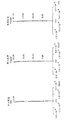
図2は、第1実施例にかかる投影光学系のレンズ構成を示す図である。図2を参照すると、第1実施例の投影光学系PLにおいて、第1レンズ群G1は、レチクル側から順に、両凸レンズL11と、両凸レンズL12と、ウェハ側に非球面形状の凹面を向けた負メニスカスレンズL13と、両凹レンズL14と、両凹レンズL15とにより構成されている。第2レンズ群G2は、レチクル側から順に、レチクル側に凹面を向けた正メニスカスレンズL21と、両凸レンズL22と、ウェハ側に平面を向けた平凸レンズL23と、ウェハ側に平面を向けた平凸レンズL24と、ウェハ側に非球面形状の凹面を向けた正メニスカスレンズL25とにより構成されている。
【0039】
第3レンズ群G3は、レチクル側から順に、両凹レンズL31と、ウェハ側に非球面形状の凹面を向けた両凹レンズL32と、レチクル側に凹面を向けた負メニスカスレンズL33とにより構成されている。第4レンズ群G4は、レチクル側から順に、レチクル側に凹面を向けた正メニスカスレンズL41と、開口絞りASと、両凸レンズL42と、両凸レンズL43と、レチクル側に凹面を向けた負メニスカスレンズL44と、両凸レンズL45と、レチクル側に凸面を向けた正メニスカスレンズL46と、レチクル側に凸面を向けた正メニスカスレンズL47とにより構成されている。第5レンズ群G5は、レチクル側から順に、ウェハ側に非球面形状の凹面を向けた正メニスカスレンズL51と、両凹レンズL52と、レチクル側に凸面を向けた正メニスカスレンズL53とから構成されている。
【0040】
第1実施例では、第1レンズ群G1において最もウェハ側(像側)に配置された両凹レンズL15は、ウェハ側に向けられた第1の凹面r1を有する。また、第3レンズ群G3において最もレチクル側(物体側)に配置された両凹レンズL31は、レチクル側に向けられた第2の凹面r2を有する。
【0041】
次の表(1)に、第1実施例にかかる投影光学系の諸元の値を掲げる。表(1)の主要諸元において、λは露光光の中心波長を、βは投影倍率を、NAは像側(ウェハ側)開口数を、Y0は最大像高(イメージフィールド半径)をそれぞれ表している。また、表(1)の光学部材諸元において、面番号はレチクル側からの面の順序を、rは各面の曲率半径(非球面の場合には頂点曲率半径:mm)を、dは各面の軸上間隔すなわち面間隔(mm)を、nは露光光の中心波長に対する屈折率を、φは各面の有効径(mm:直径)それぞれ示している。上述の表記は、以降の表(2)においても同様である。
【0042】
【表1】

図3は、第1実施例における球面収差、非点収差および歪曲収差を示す図である。また、図4は、第1実施例における横収差を示す図である。各収差図において、NAは像側の開口数を、Yは像高(mm)をそれぞれ示している。また、非点収差を示す収差図において、実線はサジタル像面を示し、破線はメリディオナル像面を示している。上述の表記は、以降の図6および図7においても同様である。各収差図から明らかなように、第1実施例では、NA=0.63という大きな開口数およびY0=21.1mmという大きな最大像高(ひいては大きなイメージフィールド)を確保しつつ、歪曲収差を含む諸収差が良好に補正されていることがわかる。
【0044】
[第2実施例]
図5は、第2実施例にかかる投影光学系のレンズ構成を示す図である。図5を参照すると、第2実施例の投影光学系PLにおいて、第1レンズ群G1は、レチクル側から順に、両凸レンズL11と、両凸レンズL12と、ウェハ側に非球面形状の凹面を向けた負メニスカスレンズL13と、両凹レンズL14と、ウェハ側に非球面形状の凹面を向けた両凹レンズL15とにより構成されている。第2レンズ群G2は、レチクル側から順に、レチクル側に凹面を向けた負メニスカスレンズL21と、レチクル側に凹面を向けた正メニスカスレンズL22と、レチクル側に凹面を向けた正メニスカスレンズL23と、両凸レンズL24と、レチクル側に凸面を向けた正メニスカスレンズL25とにより構成されている。
【0045】
第3レンズ群G3は、レチクル側から順に、ウェハ側に非球面形状の凹面を向けた両凹レンズL31と、ウェハ側に非球面形状の凹面を向けた両凹レンズL32と、レチクル側に凹面を向けた負メニスカスレンズL33とにより構成されている。第4レンズ群G4は、レチクル側から順に、レチクル側に非球面形状の凹面を向けた正メニスカスレンズL41と、開口絞りASと、両凸レンズL42と、両凸レンズL43と、レチクル側に凹面を向けた負メニスカスレンズL44と、レチクル側に凸面を向けた正メニスカスレンズ45と、レチクル側に凸面を向けた正メニスカスレンズL46と、レチクル側に凸面を向けた正メニスカスレンズL47とにより構成されている。第5レンズ群G5は、レチクル側から順に、ウェハ側に非球面形状の凹面を向けた正メニスカスレンズL51と、レチクル側に凸面を向けた負メニスカスレンズL52と、レチクル側に凸面を向けた正メニスカスレンズL53とから構成されている。
【0046】
第2実施例では、第1レンズ群G1において最もウェハ側(像側)に配置された両凹レンズL15は、ウェハ側に向けられた第1の凹面r1を有する。また、第3レンズ群G3において最もレチクル側(物体側)に配置された両凹レンズL31は、レチクル側に向けられた第2の凹面r2を有する。次の表(2)に、第2実施例にかかる投影光学系の諸元の値を掲げる。
【0047】
【表2】
図6は、第2実施例における球面収差、非点収差および歪曲収差を示す図である。また、図7は、第2実施例における横収差を示す図である。各収差図から明らかなように、第2実施例では、NA=0.65という大きな開口数およびY0=21.1mmという大きな最大像高(ひいては大きなイメージフィールド)を確保しつつ、歪曲収差を含む諸収差が良好に補正されていることがわかる。
【0049】
上述の実施形態の露光装置では、照明系によってレチクル(マスク)を照明し(照明工程)、投影光学系を用いてマスクに形成された転写用のパターンを感光性基板に露光する(露光工程)ことにより、マイクロデバイス(半導体素子、撮像素子、液晶表示素子、薄膜磁気ヘッド等)を製造することができる。以下、本実施形態の露光装置を用いて感光性基板としてのウェハ等に所定の回路パターンを形成することによって、マイクロデバイスとしての半導体デバイスを得る際の手法の一例につき図8のフローチャートを参照して説明する。
【0050】
先ず、図8のステップ301において、1ロットのウェハ上に金属膜が蒸着される。次のステップ302において、そのlロットのウェハ上の金属膜上にフォトレジストが塗布される。その後、ステップ303において、本実施形態の露光装置を用いて、マスク上のパターンの像がその投影光学系を介して、その1ロットのウェハ上の各ショット領域に順次露光転写される。その後、ステップ304において、その1ロットのウェハ上のフォトレジストの現像が行われた後、ステップ305において、その1ロットのウェハ上でレジストパターンをマスクとしてエッチングを行うことによって、マスク上のパターンに対応する回路パターンが、各ウェハ上の各ショット領域に形成される。
【0051】
その後、更に上のレイヤの回路パターンの形成等を行うことによって、半導体素子等のデバイスが製造される。上述の半導体デバイス製造方法によれば、極めて微細な回路パターンを有する半導体デバイスをスループット良く得ることができる。なお、ステップ301〜ステップ305では、ウェハ上に金属を蒸着し、その金属膜上にレジストを塗布、そして露光、現像、エッチングの各工程を行っているが、これらの工程に先立って、ウェハ上にシリコンの酸化膜を形成後、そのシリコンの酸化膜上にレジストを塗布、そして露光、現像、エッチング等の各工程を行っても良いことはいうまでもない。
【0052】
また、本実施形態の露光装置では、プレート(ガラス基板)上に所定のパターン(回路パターン、電極パターン等)を形成することによって、マイクロデバイスとしての液晶表示素子を得ることもできる。以下、図9のフローチャートを参照して、このときの手法の一例につき説明する。図9において、パターン形成工程401では、本実施形態の露光装置を用いてマスクのパターンを感光性基板(レジストが塗布されたガラス基板等)に転写露光する、所謂光リソグラフィ工程が実行される。この光リソグラフィー工程によって、感光性基板上には多数の電極等を含む所定パターンが形成される。その後、露光された基板は、現像工程、エッチング工程、レジスト剥離工程等の各工程を経ることによって、基板上に所定のパターンが形成され、次のカラーフィルター形成工程402へ移行する。
【0053】
次に、カラーフィルター形成工程402では、R(Red)、G(Green)、B(Blue)に対応した3つのドットの組がマトリックス状に多数配列されたり、またはR、G、Bの3本のストライプのフィルターの組を複数水平走査線方向に配列されたりしたカラーフィルターを形成する。そして、カラーフィルター形成工程402の後に、セル組み立て工程403が実行される。セル組み立て工程403では、パターン形成工程401にて得られた所定パターンを有する基板、およびカラーフィルター形成工程402にて得られたカラーフィルター等を用いて液晶パネル(液晶セル)を組み立てる。セル組み立て工程403では、例えば、パターン形成工程401にて得られた所定パターンを有する基板とカラーフィルター形成工程402にて得られたカラーフィルターとの間に液晶を注入して、液晶パネル(液晶セル)を製造する。
【0054】
その後、モジュール組み立て工程404にて、組み立てられた液晶パネル(液晶セル)の表示動作を行わせる電気回路、バックライト等の各部品を取り付けて液晶表示素子として完成させる。上述の液晶表示素子の製造方法によれば、極めて微細な回路パターンを有する液晶表示素子をスループット良く得ることができる。
【0055】
なお、上述の実施形態では、ウェハWの各露光領域に対してレチクルRのパターンを一括的に露光するステップ・アンド・リピート方式の露光装置に本発明を適用しているが、これに限定されることなく、ウェハWとレチクルRとを投影光学系PLに対して相対移動させつつウェハWの各露光領域に対してレチクルRのパターンを走査露光するステップ・アンド・スキャン方式の露光装置に本発明を適用することもできる。
【0056】
また、上述の実施形態では、248.4nmの波長光を供給するKrFエキシマレーザ光源を用いているが、これに限定されることなく、たとえば193nmの波長光を供給するArFエキシマレーザ光源、g線(435.8nm)やi線(365.0nm)の光を供給する水銀アークランプなどの他の適当な光源に対して本発明を適用することもできる。
【0057】
さらに、上述の実施形態では、露光装置に搭載される投影光学系に対して本発明を適用しているが、これに限定されることなく、他の一般的な投影光学系に対して本発明を適用することもできる。
【0058】
【発明の効果】
以上説明したように、本発明では、両側にほぼテレセントリックで、十分に大きな開口数および十分に広い結像領域を確保しつつ、ディストーションを含む諸収差が良好に補正された、コンパクトで高性能な投影光学系を実現することができる。したがって、本発明の投影光学系を用いる露光装置および露光方法では、レチクルやウェハの反り等に起因する像歪を抑えて、高いスループットおよび高い解像力で良好な投影露光を行うことができ、ひいては高いスループットおよび高い解像力で良好なマイクロデバイスを製造することができる。
【図面の簡単な説明】
【図1】本発明の実施形態にかかる投影光学系を備えた露光装置の構成を概略的に示す図である。
【図2】第1実施例にかかる投影光学系のレンズ構成を示す図である。
【図3】第1実施例における球面収差、非点収差および歪曲収差を示す図である。
【図4】第1実施例における横収差を示す図である。
【図5】第2実施例にかかる投影光学系のレンズ構成を示す図である。
【図6】第2実施例における球面収差、非点収差および歪曲収差を示す図である。
【図7】第2実施例における横収差を示す図である。
【図8】マイクロデバイスとしての半導体デバイスを得る際の手法のフローチャートである。
【図9】マイクロデバイスとしての液晶表示素子を得る際の手法のフローチャートである。
【符号の説明】
LS 光源
IL 照明光学系
R レチクル
RS レチクルステージ
PL 投影光学系
W ウェハ
WS ウェハステージ
AS 開口絞り
G1 第1レンズ群
G2 第2レンズ群
G3 第3レンズ群
G4 第4レンズ群
G5 第5レンズ群
Li レンズ成分[0001]
BACKGROUND OF THE INVENTION
The present invention relates to a projection optical system, an exposure apparatus, and an exposure method, and more particularly to a projection optical system suitable for an exposure apparatus used when manufacturing a microdevice such as a semiconductor element or a liquid crystal display element in a photolithography process. is there.
[0002]
[Prior art]
When manufacturing a semiconductor element or the like, an exposure apparatus is used that transfers a pattern image of a reticle as a mask onto a resist-coated wafer (or glass plate or the like) via a projection optical system. In this type of exposure apparatus, it is desired that the resolution of the projection optical system be improved as the pattern of a semiconductor integrated circuit or the like becomes finer. In order to improve the resolution of the projection optical system, it is conceivable to shorten the wavelength of the exposure light or increase the numerical aperture.
[0003]
In recent years, exposure light is shifting from g-rays (436 nm) and i-rays (365 nm) of mercury lamps to shorter wavelength KrF excimer laser light (248 nm) and ArF excimer laser light (193 nm). However, if the wavelength of the exposure light is shortened in order to improve the resolution of the projection optical system, the types of optical materials having a predetermined transmittance that can be used for the optical members constituting the projection optical system are limited. This makes it difficult to design a projection optical system. Specifically, in a projection optical system using KrF excimer laser light or ArF excimer laser light, usable optical materials are substantially limited to quartz, fluorite and the like having a relatively low refractive index.
[0004]
Further, in the projection optical system, as the resolution is improved, the demand for reducing the image distortion is getting stricter. Here, image distortion is not only image distortion caused by distortion (distortion aberration) of the projection optical system but also image distortion caused by warpage of the wafer set on the image plane of the projection optical system and on which the reticle pattern is baked. In addition, there is image distortion caused by warping of a reticle that is set on the object plane of the projection optical system and on which a circuit pattern or the like is drawn.
[0005]
[Problems to be solved by the invention]
As described above, in the prior art, as the transfer pattern is miniaturized, the demand for reducing image distortion has become more severe. In order to reduce the influence of the warpage of the wafer on the image distortion, a so-called image side telecentric projection optical system in which the exit pupil of the projection optical system is positioned far from the image plane has been proposed. In addition, in order to reduce image distortion caused by reticle warpage, proposals have been made to position the entrance pupil of the projection optical system relatively far from the object plane.
[0006]
However, in the prior art, various proposals have been made for a projection optical system having high resolution, but a sufficiently wide effective exposure area (image field: imaging area) is not ensured. For this reason, so-called step-and-scan projection exposure, in which the reticle pattern is scanned and exposed to each exposure area of the wafer while moving the reticle and wafer relative to the projection optical system, has a sufficiently high throughput. Could not be realized. Thus, in order to realize a high-throughput exposure apparatus, it is desired to secure a wider image field on the wafer, that is, to widen the field.
[0007]
Further, as described above, when the exposure light is shortened in order to improve the resolving power, the transmittance of the optical material constituting the projection optical system is lowered, which can be used to ensure high transmittance. The types of optical materials are also limited. Furthermore, the decrease in transmittance not only causes loss of light quantity, but part of the lost light is absorbed by the optical member, and the change in the refractive index of the optical member and the optical surface (lens) by the absorbed light being converted into heat. As a result, the imaging performance of the projection optical system is deteriorated.
[0008]
In addition, it is necessary to correct aberrations in order to widen the field and increase the resolution, but it is extremely difficult to correct aberrations over a wide exposure area using a limited type of optical material. .
[0009]
The present invention has been made in view of the above-described problems, and various aberrations including distortion are corrected satisfactorily while ensuring a sufficiently large numerical aperture and a sufficiently wide imaging region on both sides. An object of the present invention is to provide a compact and high-performance projection optical system. Another object of the present invention is to provide an exposure apparatus and an exposure method capable of performing good projection exposure with high throughput and high resolution using a compact and high-performance projection optical system.
[0010]
[Means for Solving the Problems]
In order to solve the above problems, in the first embodiment of the present invention, in the projection optical system for forming the image of the first surface on the second surface,
In order from the first surface side, a first lens group having negative refractive power, a second lens group having positive refractive power, a third lens group having negative refractive power, and positive refractive power A fourth lens group and a fifth lens group having positive refractive power;
The first lens group includes at least two negative lenses and at least one aspheric optical surface;
The second lens group includes at least four positive lenses arranged continuously on the second surface side,
The third lens group includes at least two negative lenses and at least one aspheric optical surface;
The fourth lens group includes at least five positive lenses, at least one negative lens, and at least one aspheric optical surface;
The fifth lens group includes at least one negative lens;
The lens arranged closest to the second surface side in the first lens group has a first concave surface directed to the second surface,
The lens arranged closest to the first surface in the third lens group has a second concave surface directed to the first surface,
When the axial distance between the fourth lens group and the fifth lens group is D45, and the distance between the first surface and the second surface is L,
0.02 <D45 / L <0.1
A projection optical system characterized by satisfying the above conditions is provided.
[0011]
According to a preferred aspect of the first form, the maximum exit angle (degree) α1 of light emitted from the first concave surface in the first lens group and the second concave surface in the third lens group. The maximum incident angle (degree) α2 of incident light satisfies the conditions of 35 <α1 <60, 35 <α2 <60. The effective diameter of the first concave surface in the first lens group is φ1, the effective diameter of the second concave surface in the third lens group is φ2, and the maximum effective diameter of the second lens group is When φmax, it is preferable to satisfy the conditions of 0.5 <φ1 / φmax <0.8 and 0.5 <φ2 / φmax <0.8.
[0012]
According to a preferred aspect of the first aspect, all the optical members constituting the projection optical system are formed of an optical material having a refractive index of 1.6 or less. The focal length of the first lens group is f1, the focal length of the second lens group is f2, the focal length of the third lens group is f3, and the focal length of the fourth lens group is f4. When the focal length of the fifth lens group is f5 and the distance between the first surface and the second surface is L,
0.05 <| f1 | / L <0.5
0.02 <f2 / L <0.2
0.01 <| f3 | / L <0.1
0.03 <f4 / L <0.3
0.1 <f5 / L <1
It is preferable to satisfy the following conditions.
[0013]
In the second embodiment of the present invention, an illumination system for illuminating the mask disposed on the first surface and an image of a pattern formed on the mask are formed on the photosensitive substrate disposed on the second surface. An exposure apparatus is provided that includes the projection optical system according to the first embodiment.
[0014]
In the third embodiment of the present invention, the mask disposed on the first surface is illuminated, and the pattern formed on the mask is the photosensitive substrate disposed on the second surface via the projection optical system of the first embodiment. Provided is an exposure method characterized by performing projection exposure on top.
[0015]
DETAILED DESCRIPTION OF THE INVENTION
In the projection optical system of the present invention, in the basic configuration having negative, positive, negative, positive, and positive refractive power arrangements in order from the object surface (first surface) side, the first lens unit to the fifth lens unit are respectively It has the following characteristic configuration. That is, the first lens group includes at least two negative lenses and at least one aspherical optical surface. With this configuration, the first lens unit, which has an aspherical optical surface in particular, contributes mainly to the distortion correction function and Petzval sum correction while maintaining telecentricity. It has the function to achieve
[0016]
The second lens group includes at least four positive lenses arranged continuously on the image surface (second surface) side. With this configuration, the second lens group has a function of generating positive distortion and correcting negative distortion generated in the third lens group, the fourth lens group, and the fifth lens group in a balanced manner. The third lens group includes at least two negative lenses and at least one aspherical optical surface. With this configuration, the third lens unit mainly contributes to the correction of Petzval sum and suppresses the occurrence of higher-order spherical aberration and coma aberration, and has a flattened image surface, particularly by the configuration having an aspherical optical surface. It has the function to achieve
[0017]
The fourth lens group includes at least five positive lenses, at least one negative lens, and at least one aspherical optical surface. With this configuration, the fourth lens group has a function of guiding a light beam on the image plane to form an image while suppressing generation of spherical aberration, particularly by a configuration having an aspherical optical surface. The fifth lens group includes at least one negative lens. With this configuration, the fifth lens group has a function of forming a light beam on the image surface while suppressing spherical aberration so that a sufficiently large numerical aperture can be secured on the image side.
[0018]
In the projection optical system of the present invention, the lens disposed closest to the image plane in the first lens group has a first concave surface directed toward the image plane, and is disposed closest to the object plane in the third lens group. The shaped lens has a characteristic configuration with a second concave surface directed toward the object plane. The first lens group and the third lens group adjacent to the second lens group respectively have a first concave surface and a second concave surface toward the second lens group, so that the positive refractive power of the second lens group ( The aberration of the outer coma generated by (power) can be corrected with good balance. The configuration having the first concave surface and the second concave surface is particularly effective for aberration correction of a projection optical system having a large image-side numerical aperture and a wide imaging region.
[0019]
Furthermore, in the projection optical system of the present invention, the following conditional expression (1) is satisfied in order to correct the Petzval sum while suppressing an increase in diameter. In conditional expression (1), D45 is the axial distance between the fourth lens group and the fifth lens group, and L is the distance between the object plane (first surface) and the image plane (second surface).
0.02 <D45 / L <0.1 (1)
[0020]
If the lower limit of conditional expression (1) is not reached, correction of the Petzval sum becomes difficult, and flattening of the image plane cannot be achieved. On the other hand, if the upper limit of conditional expression (1) is exceeded, the optical system will be lengthened. Satisfying conditional expression (1) is particularly effective for aberration correction of a projection optical system having a large image-side numerical aperture and a wide imaging area.
[0021]
In the present invention, the maximum emission angle (degree) α1 of the light emitted from the first concave surface in the first lens group and the maximum incident angle of the light incident on the second concave surface in the third lens group ( Degree) α2 preferably satisfies the following conditional expressions (2) and (3).
35 <α1 <60 (2)
35 <α2 <60 (3)
[0022]
By satisfying conditional expressions (2) and (3), it is possible to correct the aberration of the outer coma caused by the positive refractive power of the second lens group in a well-balanced manner. That is, if the lower limit value of conditional expressions (2) and (3) is not reached, it is difficult to correct the outer frame generated in the second lens group in a well-balanced manner, which is not preferable. On the other hand, if the upper limit value of conditional expressions (2) and (3) is exceeded, higher-order coma aberration generated on the first concave surface and the second concave surface increases, respectively, which is not preferable. Satisfying conditional expressions (2) and (3) is particularly effective for correcting aberrations in a projection optical system having a large image-side numerical aperture and a wide imaging area.
[0023]
In the present invention, when the maximum effective diameter (diameter) of the second lens group is φmax, the effective diameter (diameter) φ1 of the first concave surface in the first lens group and the second effective diameter (diameter) in the third lens group. It is preferable that the effective diameter (diameter) φ2 of the concave surface satisfies the following conditional expressions (4) and (5).
0.5 <φ1 / φmax <0.8 (4)
0.5 <φ2 / φmax <0.8 (5)
[0024]
If the lower limit value of conditional expressions (4) and (5) is not reached, the maximum effective diameter φmax of the second lens group becomes too large, and the diameter of the optical system increases, which is not preferable. On the other hand, when the upper limit value of conditional expressions (4) and (5) is exceeded, the effective diameter φ1 of the first concave surface and the effective diameter φ2 of the second concave surface become too large, and coma aberration generated in the second lens group. Cannot be corrected completely, and correction of Petzval sum becomes difficult.
[0025]
In the present invention, the focal length f1 of the first lens group, the focal length f2 of the second lens group, the focal length f3 of the third lens group, the focal length f4 of the fourth lens group, and the focal length of the fifth lens group. It is preferable that f5 satisfies the following conditional expressions (6) to (10).
0.05 <| f1 | / L <0.5 (6)
0.02 <f2 / L <0.2 (7)
0.01 <| f3 | / L <0.1 (8)
0.03 <f4 / L <0.3 (9)
0.1 <f5 / L <1 (10)
[0026]
By satisfying conditional expressions (6) to (10), it is possible to correct each aberration in a well-balanced manner while realizing a compact projection optical system having a large image-side numerical aperture and a wide imaging area. Specifically, if the lower limit value of conditional expression (6) is not reached, negative distortion increases, and if it exceeds the upper limit value, it becomes difficult to correct the telecentricity. Further, if the lower limit value of conditional expression (7) is not reached, higher-order coma aberration increases, and if it exceeds the upper limit value, negative distortion becomes insufficiently corrected.
[0027]
Further, if the lower limit value of conditional expression (8) is not reached, high-order coma aberration and high-order spherical aberration will increase, and if it exceeds the upper limit value, the Petzval sum becomes insufficiently corrected. If the lower limit value of conditional expression (9) is not reached, higher-order spherical aberration increases, and if it exceeds the upper limit value, the optical system becomes longer, which is not preferable. Further, if the lower limit value of conditional expression (10) is not reached, higher order coma aberration and higher order spherical aberration will increase, and if the upper limit value is exceeded, the optical system will become longer, which is not preferable.
[0028]
In the present invention, it is preferable that all optical members constituting the projection optical system are formed of an optical material having a refractive index of 1.6 or less. In this case, an optical material having a refractive index of 1.6 or less, that is, an optical material having a relatively low refractive index can secure a high transmittance even for light with a short wavelength, and thus the short wavelength of the used light. Therefore, high resolution of the projection optical system can be achieved. Note that the projection optical system of the present invention is configured to be a substantially telecentric optical system on both the object side and the image side, thereby affecting the image distortion on the object plane side (such as reticle warping when applied to an exposure apparatus). ) And the influence on the image surface side image distortion (image distortion caused by warpage of the wafer when applied to an exposure apparatus) can be reduced.
[0029]
As described above, in the present invention, a compact and high-performance projection that is substantially telecentric on both sides, has a sufficiently large numerical aperture and a sufficiently wide imaging region, and various aberrations including distortion are well corrected. An optical system can be realized. Therefore, in the exposure apparatus and exposure method using the projection optical system of the present invention, it is possible to perform good projection exposure with high throughput and high resolution, and thus it is possible to manufacture good microdevices with high throughput and high resolution. .
[0030]
Embodiments of the present invention will be described with reference to the accompanying drawings.
FIG. 1 is a drawing schematically showing a configuration of an exposure apparatus provided with a projection optical system according to an embodiment of the present invention. In FIG. 1, the Z axis is parallel to the optical axis AX of the projection optical system PL, the Y axis is parallel to the paper surface of FIG. 1 in a plane perpendicular to the optical axis AX, and the plane is perpendicular to the optical axis AX. The X axis is set perpendicular to the paper surface of FIG.
[0031]
The exposure apparatus shown in FIG. 1 includes, for example, a KrF excimer laser light source (wavelength 248.4 nm) as a light source LS for supplying illumination light. The light emitted from the light source LS illuminates a reticle (mask) R as a projection master on which a predetermined pattern is formed, via the illumination optical system IL. The illumination optical system IL includes a fly-eye lens for uniforming the illuminance distribution of exposure light, an illumination aperture stop, a variable field stop (reticle blind), a condenser lens system, and the like.
[0032]
The reticle R is held parallel to the XY plane on the reticle stage RS via the reticle holder RH. Reticle stage RS can be moved two-dimensionally along the reticle plane (ie, XY plane) by the action of a drive system (not shown), and its position coordinates are measured by interferometer RIF using reticle moving mirror RM. And the position is controlled. Light from the pattern formed on the reticle R forms a reticle pattern image on the wafer W (photosensitive substrate) coated with a photoresist via the projection optical system PL.
[0033]
The projection optical system PL has a variable aperture stop AS (not shown in FIG. 1) disposed in the vicinity of the pupil position, and is substantially telecentric on both the reticle R side and the wafer W side. . Then, an image of the secondary light source on the illumination pupil plane of the illumination optical system is formed at the pupil position of the projection optical system PL, and the wafer W is Koehler illuminated with light via the projection optical system PL. The wafer W is held parallel to the XY plane on the wafer stage WS via a wafer table (wafer holder) WT.
[0034]
The wafer stage WS can be moved two-dimensionally along the wafer surface (that is, the XY plane) by the action of a drive system (not shown), and its position coordinates are measured by an interferometer WIF using a wafer moving mirror WM. In addition, the position is controlled. Thus, in the present embodiment, the operation of collectively exposing the pattern of the reticle R to each exposure region while two-dimensionally driving and controlling the wafer W in the plane orthogonal to the optical axis AX of the projection optical system PL. By repeating, that is, by the step-and-repeat method, the pattern of the reticle R is sequentially exposed in each exposure region of the wafer W.
[0035]
Hereinafter, examples of the projection optical system PL of the present embodiment will be described based on specific numerical examples. In each example, the projection optical system PL includes, in order from the reticle side, a first lens group G1 having a negative refractive power, a second lens group G2 having a positive refractive power, and a third lens having a negative refractive power. The lens group G3 includes a fourth lens group G4 having a positive refractive power and a fifth lens group G5 having a positive refractive power. In each embodiment, all lens components constituting the projection optical system PL are made of quartz (SiO 2 ), and the center wavelength of the KrF excimer laser light supplied from the light source LS is 248.4 nm. The refractive index of quartz glass with respect to wavelength is 1.50839.
[0036]
In each embodiment, the aspherical surface has a height in the direction perpendicular to the optical axis as y, and the distance along the optical axis from the tangential plane at the apex of the aspherical surface to the position on the aspherical surface at height y ( When the sag amount is z, the apex radius of curvature is r, the conic coefficient is κ, and the nth-order aspheric coefficient is C n , the following equation (a) is obtained. In Tables (1) and (2), which will be described later, an aspherical lens surface is marked with an asterisk (*) on the right side of the surface number.
[0037]
[Expression 1]
z = (y 2 / r) / [1+ {1− (1 + κ) · y 2 / r 2 } 1/2 ]
+ C 4 · y 4 + C 6 · y 6 + C 8 · y 8 + C 10 · y 10 + (a)
[0038]
[First embodiment]
FIG. 2 is a diagram illustrating a lens configuration of the projection optical system according to the first example. Referring to FIG. 2, in the projection optical system PL of the first example, the first lens group G1 has a biconvex lens L11, a biconvex lens L12, and an aspheric concave surface facing the wafer side in order from the reticle side. The lens includes a negative meniscus lens L13, a biconcave lens L14, and a biconcave lens L15. The second lens group G2, in order from the reticle side, includes a positive meniscus lens L21 having a concave surface facing the reticle side, a biconvex lens L22, a plano-convex lens L23 having a plane surface on the wafer side, and a flat surface having a plane surface on the wafer side. The lens includes a convex lens L24 and a positive meniscus lens L25 having an aspheric concave surface facing the wafer.
[0039]
The third lens group G3 includes, in order from the reticle side, a biconcave lens L31, a biconcave lens L32 having an aspheric concave surface facing the wafer side, and a negative meniscus lens L33 having a concave surface facing the reticle side. . The fourth lens group G4 includes, in order from the reticle side, a positive meniscus lens L41 having a concave surface directed to the reticle side, an aperture stop AS, a biconvex lens L42, a biconvex lens L43, and a negative meniscus lens having a concave surface directed to the reticle side. L44, a biconvex lens L45, a positive meniscus lens L46 having a convex surface on the reticle side, and a positive meniscus lens L47 having a convex surface on the reticle side. The fifth lens group G5 includes, in order from the reticle side, a positive meniscus lens L51 having an aspheric concave surface facing the wafer side, a biconcave lens L52, and a positive meniscus lens L53 having a convex surface facing the reticle side. Yes.
[0040]
In the first example, the biconcave lens L15 arranged closest to the wafer side (image side) in the first lens group G1 has a first concave surface r1 directed toward the wafer side. In addition, the biconcave lens L31 arranged on the most reticle side (object side) in the third lens group G3 has a second concave surface r2 directed toward the reticle side.
[0041]
The following table (1) lists the values of the specifications of the projection optical system according to the first example. In the main specifications of Table (1), λ is the center wavelength of the exposure light, β is the projection magnification, NA is the image side (wafer side) numerical aperture, and Y 0 is the maximum image height (image field radius). Represents. In the optical member specifications of Table (1), the surface number is the order of the surfaces from the reticle side, r is the radius of curvature of each surface (vertical curvature radius: mm in the case of an aspheric surface), and d is each The axial distance between the surfaces, that is, the surface distance (mm), n represents the refractive index with respect to the center wavelength of the exposure light, and φ represents the effective diameter (mm: diameter) of each surface. The above notation is the same in the following table (2).
[0042]
[Table 1]
FIG. 3 is a diagram showing spherical aberration, astigmatism, and distortion in the first example. FIG. 4 is a diagram showing transverse aberration in the first example. In each aberration diagram, NA represents the numerical aperture on the image side, and Y represents the image height (mm). In the aberration diagrams showing astigmatism, the solid line shows the sagittal image plane, and the broken line shows the meridional image plane. The above notation is the same in the following FIG. 6 and FIG. As is apparent from each aberration diagram, in the first example, distortion is reduced while ensuring a large numerical aperture of NA = 0.63 and a large maximum image height (and a large image field) of Y 0 = 21.1 mm. It can be seen that the various aberrations are corrected well.
[0044]
[Second Embodiment]
FIG. 5 is a diagram showing a lens configuration of the projection optical system according to the second example. Referring to FIG. 5, in the projection optical system PL of the second example, the first lens group G1 has a biconvex lens L11, a biconvex lens L12, and an aspheric concave surface facing the wafer side in order from the reticle side. The lens includes a negative meniscus lens L13, a biconcave lens L14, and a biconcave lens L15 having an aspheric concave surface facing the wafer side. The second lens group G2, in order from the reticle side, includes a negative meniscus lens L21 having a concave surface on the reticle side, a positive meniscus lens L22 having a concave surface on the reticle side, and a positive meniscus lens L23 having a concave surface on the reticle side. And a biconvex lens L24 and a positive meniscus lens L25 having a convex surface facing the reticle.
[0045]
The third lens group G3 includes, in order from the reticle side, a biconcave lens L31 with an aspherical concave surface facing the wafer, a biconcave lens L32 with an aspherical concave surface facing the wafer, and a concave surface facing the reticle side. And a negative meniscus lens L33. The fourth lens group G4 includes, in order from the reticle side, a positive meniscus lens L41 having an aspheric concave surface facing the reticle side, an aperture stop AS, a biconvex lens L42, a biconvex lens L43, and a concave surface facing the reticle side. Negative meniscus lens L44, positive meniscus lens 45 having a convex surface on the reticle side, positive meniscus lens L46 having a convex surface on the reticle side, and positive meniscus lens L47 having a convex surface on the reticle side. . The fifth lens group G5 includes, in order from the reticle side, a positive meniscus lens L51 having an aspheric concave surface facing the wafer, a negative meniscus lens L52 having a convex surface facing the reticle, and a positive meniscus lens L52 having a convex surface facing the reticle. And a meniscus lens L53.
[0046]
In the second example, the biconcave lens L15 disposed on the most wafer side (image side) in the first lens group G1 has a first concave surface r1 directed toward the wafer side. In addition, the biconcave lens L31 arranged on the most reticle side (object side) in the third lens group G3 has a second concave surface r2 directed toward the reticle side. The following table (2) lists the values of the specifications of the projection optical system according to the second example.
[0047]
[Table 2]
FIG. 6 is a diagram showing spherical aberration, astigmatism, and distortion in the second example. FIG. 7 is a diagram showing transverse aberration in the second example. As is apparent from each aberration diagram, in the second embodiment, distortion is reduced while ensuring a large numerical aperture of NA = 0.65 and a large maximum image height (and thus a large image field) of Y 0 = 21.1 mm. It can be seen that the various aberrations are corrected well.
[0049]
In the exposure apparatus of the above-described embodiment, the reticle (mask) is illuminated by the illumination system (illumination process), and the transfer pattern formed on the mask is exposed to the photosensitive substrate using the projection optical system (exposure process). Thus, a micro device (semiconductor element, imaging element, liquid crystal display element, thin film magnetic head, etc.) can be manufactured. Hereinafter, referring to the flowchart of FIG. 8 for an example of a technique for obtaining a semiconductor device as a micro device by forming a predetermined circuit pattern on a wafer or the like as a photosensitive substrate using the exposure apparatus of the present embodiment. I will explain.
[0050]
First, in step 301 of FIG. 8, a metal film is deposited on one lot of wafers. In the next step 302, a photoresist is applied on the metal film on the lot of wafers. Thereafter, in step 303, using the exposure apparatus of the present embodiment, the image of the pattern on the mask is sequentially exposed and transferred to each shot area on the wafer of one lot via the projection optical system. Thereafter, in step 304, the photoresist on the one lot of wafers is developed, and in step 305, the resist pattern is etched on the one lot of wafers to form a pattern on the mask. Corresponding circuit patterns are formed in each shot area on each wafer.
[0051]
Thereafter, a device pattern such as a semiconductor element is manufactured by forming a circuit pattern of an upper layer. According to the semiconductor device manufacturing method described above, a semiconductor device having an extremely fine circuit pattern can be obtained with high throughput. In steps 301 to 305, a metal is deposited on the wafer, a resist is applied on the metal film, and exposure, development, and etching processes are performed. Prior to these processes, on the wafer. It is needless to say that after forming a silicon oxide film, a resist may be applied on the silicon oxide film, and steps such as exposure, development, and etching may be performed.
[0052]
In the exposure apparatus of this embodiment, a liquid crystal display element as a micro device can be obtained by forming a predetermined pattern (circuit pattern, electrode pattern, etc.) on a plate (glass substrate). Hereinafter, an example of the technique at this time will be described with reference to the flowchart of FIG. In FIG. 9, in a pattern formation process 401, a so-called photolithography process is performed in which the exposure pattern of the present embodiment is used to transfer and expose a mask pattern onto a photosensitive substrate (such as a glass substrate coated with a resist). By this photolithography process, a predetermined pattern including a large number of electrodes and the like is formed on the photosensitive substrate. Thereafter, the exposed substrate undergoes steps such as a developing step, an etching step, and a resist stripping step, whereby a predetermined pattern is formed on the substrate, and the process proceeds to the next color filter forming step 402.
[0053]
Next, in the color filter forming step 402, a large number of sets of three dots corresponding to R (Red), G (Green), and B (Blue) are arranged in a matrix or three of R, G, and B A color filter is formed by arranging a plurality of stripe filter sets in the horizontal scanning line direction. Then, after the color filter forming step 402, a cell assembly step 403 is executed. In the cell assembly step 403, a liquid crystal panel (liquid crystal cell) is assembled using the substrate having the predetermined pattern obtained in the pattern formation step 401, the color filter obtained in the color filter formation step 402, and the like. In the cell assembly step 403, for example, liquid crystal is injected between the substrate having the predetermined pattern obtained in the pattern formation step 401 and the color filter obtained in the color filter formation step 402, and a liquid crystal panel (liquid crystal cell) is obtained. ).
[0054]
Thereafter, in a module assembling step 404, components such as an electric circuit and a backlight for performing a display operation of the assembled liquid crystal panel (liquid crystal cell) are attached to complete a liquid crystal display element. According to the above-described method for manufacturing a liquid crystal display element, a liquid crystal display element having an extremely fine circuit pattern can be obtained with high throughput.
[0055]
In the above-described embodiment, the present invention is applied to a step-and-repeat type exposure apparatus that collectively exposes the pattern of the reticle R to each exposure region of the wafer W. However, the present invention is not limited to this. And a step-and-scan type exposure apparatus that scans and exposes the pattern of the reticle R to each exposure area of the wafer W while moving the wafer W and the reticle R relative to the projection optical system PL. The invention can also be applied.
[0056]
In the above-described embodiment, a KrF excimer laser light source that supplies light with a wavelength of 248.4 nm is used. However, the present invention is not limited to this. For example, an ArF excimer laser light source that supplies light with a wavelength of 193 nm, g-line The present invention can also be applied to other suitable light sources such as mercury arc lamps that supply (435.8 nm) or i-line (365.0 nm) light.
[0057]
Furthermore, in the above-described embodiment, the present invention is applied to the projection optical system mounted on the exposure apparatus. However, the present invention is not limited to this and is applied to other general projection optical systems. Can also be applied.
[0058]
【The invention's effect】
As described above, according to the present invention, a compact, high-performance, which is substantially telecentric on both sides, has a sufficiently large numerical aperture and a sufficiently wide imaging region, and various aberrations including distortion are well corrected. A projection optical system can be realized. Therefore, in the exposure apparatus and exposure method using the projection optical system of the present invention, it is possible to suppress the image distortion caused by the warp of the reticle or wafer, and to perform good projection exposure with high throughput and high resolution, and consequently high. Good microdevices can be manufactured with high throughput and high resolution.
[Brief description of the drawings]
FIG. 1 is a drawing schematically showing a configuration of an exposure apparatus provided with a projection optical system according to an embodiment of the present invention.
FIG. 2 is a diagram showing a lens configuration of a projection optical system according to the first example.
FIG. 3 is a diagram showing spherical aberration, astigmatism, and distortion in the first example.
FIG. 4 is a diagram showing transverse aberration in the first example.
FIG. 5 is a diagram showing a lens configuration of a projection optical system according to a second example.
FIG. 6 is a diagram showing spherical aberration, astigmatism, and distortion in the second example.
FIG. 7 is a diagram showing transverse aberration in the second example.
FIG. 8 is a flowchart of a method for obtaining a semiconductor device as a micro device.
FIG. 9 is a flowchart of a method for obtaining a liquid crystal display element as a micro device.
[Explanation of symbols]
LS light source IL illumination optical system R reticle RS reticle stage PL projection optical system W wafer WS wafer stage AS aperture stop G1 first lens group G2 second lens group G3 third lens group G4 fourth lens group G5 fifth lens group Li lens component
Claims (8)
前記第1面側から順に、負の屈折力を有する第1レンズ群と、正の屈折力を有する第2レンズ群と、負の屈折力を有する第3レンズ群と、正の屈折力を有する第4レンズ群と、正の屈折力を有する第5レンズ群とを備え、
前記第1レンズ群は、少なくとも2つの負レンズと、少なくとも1つの非球面状の光学面とを含み、
前記第2レンズ群は、前記第2面側に連続して配置された少なくとも4つの正レンズを含み、
前記第3レンズ群は、少なくとも2つの負レンズと、少なくとも1つの非球面状の光学面とを含み、
前記第4レンズ群は、少なくとも5つの正レンズと、少なくとも1つの負レンズと、少なくとも1つの非球面状の光学面とを含み、
前記第5レンズ群は、少なくとも1つの負レンズを含み、
前記第1レンズ群において最も前記第2面側に配置されたレンズは、前記第2面に向けられた第1の凹面を有し、
前記第3レンズ群において最も前記第1面側に配置されたレンズは、前記第1面に向けられた第2の凹面を有し、
前記第4レンズ群と前記第5レンズ群との軸上間隔をD45とし、前記第1面と前記第2面との距離をLとするとき、
0.035≦D45/L<0.1
の条件を満足することを特徴とする投影光学系。In a projection optical system for forming an image of a first surface on a second surface,
In order from the first surface side, a first lens group having negative refractive power, a second lens group having positive refractive power, a third lens group having negative refractive power, and positive refractive power A fourth lens group and a fifth lens group having positive refractive power;
The first lens group includes at least two negative lenses and at least one aspheric optical surface;
The second lens group includes at least four positive lenses arranged continuously on the second surface side,
The third lens group includes at least two negative lenses and at least one aspheric optical surface;
The fourth lens group includes at least five positive lenses, at least one negative lens, and at least one aspheric optical surface;
The fifth lens group includes at least one negative lens;
The lens arranged closest to the second surface side in the first lens group has a first concave surface directed to the second surface,
The lens arranged closest to the first surface in the third lens group has a second concave surface directed to the first surface,
When the axial distance between the fourth lens group and the fifth lens group is D45, and the distance between the first surface and the second surface is L,
0.035 ≦ D45 / L <0.1
A projection optical system characterized by satisfying the following conditions.
35<α1<60
35<α2<60
の条件を満足することを特徴とする請求項1に記載の投影光学系。The maximum emission angle (degree) α1 of light emitted from the first concave surface in the first lens group and the maximum incident angle (degree) of light incident on the second concave surface in the third lens group α2 is
35 <α1 <60
35 <α2 <60
The projection optical system according to claim 1, wherein the following condition is satisfied.
0.5<φ1/φmax<0.8
0.5<φ2/φmax<0.8
の条件を満足することを特徴とする請求項1または2に記載の投影光学系。The effective diameter of the first concave surface in the first lens group is φ1, the effective diameter of the second concave surface in the third lens group is φ2, and the maximum effective diameter of the second lens group is φmax. and when,
0.5 <φ1 / φmax <0.8
0.5 <φ2 / φmax <0.8
The projection optical system according to claim 1, wherein the following condition is satisfied.
0.05<|f1|/L<0.5
0.02<f2/L<0.2
0.01<|f3|/L<0.1
0.03<f4/L<0.3
0.1<f5/L<1
の条件を満足することを特徴とする請求項1乃至4のいずれか1項に記載の投影光学系。The focal length of the first lens group is f1, the focal length of the second lens group is f2, the focal length of the third lens group is f3, and the focal length of the fourth lens group is f4. When the focal length of the five lens groups is f5 and the distance between the first surface and the second surface is L,
0.05 <| f1 | / L <0.5
0.02 <f2 / L <0.2
0.01 <| f3 | / L <0.1
0.03 <f4 / L <0.3
0.1 <f5 / L <1
The projection optical system according to claim 1, wherein the following condition is satisfied.
Priority Applications (1)
| Application Number | Priority Date | Filing Date | Title |
|---|---|---|---|
| JP2003003867A JP4300509B2 (en) | 2003-01-10 | 2003-01-10 | Projection optical system, exposure apparatus, and exposure method |
Applications Claiming Priority (1)
| Application Number | Priority Date | Filing Date | Title |
|---|---|---|---|
| JP2003003867A JP4300509B2 (en) | 2003-01-10 | 2003-01-10 | Projection optical system, exposure apparatus, and exposure method |
Publications (3)
| Publication Number | Publication Date |
|---|---|
| JP2004219501A JP2004219501A (en) | 2004-08-05 |
| JP2004219501A5 JP2004219501A5 (en) | 2008-02-28 |
| JP4300509B2 true JP4300509B2 (en) | 2009-07-22 |
Family
ID=32895006
Family Applications (1)
| Application Number | Title | Priority Date | Filing Date |
|---|---|---|---|
| JP2003003867A Expired - Fee Related JP4300509B2 (en) | 2003-01-10 | 2003-01-10 | Projection optical system, exposure apparatus, and exposure method |
Country Status (1)
| Country | Link |
|---|---|
| JP (1) | JP4300509B2 (en) |
Families Citing this family (5)
| Publication number | Priority date | Publication date | Assignee | Title |
|---|---|---|---|---|
| US8208198B2 (en) | 2004-01-14 | 2012-06-26 | Carl Zeiss Smt Gmbh | Catadioptric projection objective |
| US20080151365A1 (en) | 2004-01-14 | 2008-06-26 | Carl Zeiss Smt Ag | Catadioptric projection objective |
| KR20170129271A (en) | 2004-05-17 | 2017-11-24 | 칼 짜이스 에스엠티 게엠베하 | Catadioptric projection objective with intermediate images |
| CN102662307B (en) * | 2012-05-02 | 2014-03-12 | 中国科学院光电技术研究所 | High-resolution projection optical system |
| CN103278912B (en) * | 2013-06-19 | 2015-07-08 | 中国科学院光电技术研究所 | Reflective type ultra-violet lithography objective lens |
-
2003
- 2003-01-10 JP JP2003003867A patent/JP4300509B2/en not_active Expired - Fee Related
Also Published As
| Publication number | Publication date |
|---|---|
| JP2004219501A (en) | 2004-08-05 |
Similar Documents
| Publication | Publication Date | Title |
|---|---|---|
| US6259508B1 (en) | Projection optical system and exposure apparatus and method | |
| KR100866818B1 (en) | Projection optical system and exposure apparatus comprising the same | |
| JP3750123B2 (en) | Projection optical system | |
| JP3819048B2 (en) | Projection optical system, exposure apparatus including the same, and exposure method | |
| JP3925576B2 (en) | Projection optical system, exposure apparatus including the optical system, and device manufacturing method using the apparatus | |
| US6867922B1 (en) | Projection optical system and projection exposure apparatus using the same | |
| JP4779394B2 (en) | Projection optical system, exposure apparatus, and exposure method | |
| JPH1079345A (en) | Projection optical system and exposing device | |
| JP4370582B2 (en) | Projection optical system, exposure apparatus, and exposure method | |
| JP2006086141A (en) | Projection optical system, aligner, and method of exposure | |
| JP2007206319A (en) | Reflective/refractive optical system, exposure apparatus and method of manufacturing micro device | |
| KR100522503B1 (en) | Projection optical system and projection exposure apparatus with the same, and device manufacturing method | |
| JP4300509B2 (en) | Projection optical system, exposure apparatus, and exposure method | |
| KR100386870B1 (en) | Projection Optics and Exposure Equipment | |
| JP4228130B2 (en) | Projection optical system, exposure apparatus, and device manufacturing method | |
| KR100989606B1 (en) | Projection optical system, exposure apparatus, and method of manufacturing a device | |
| JP2002244035A (en) | Projection optical system and exposure device provided with it | |
| JP2005115127A (en) | Catadioptric projection optical system, exposure device and exposing method | |
| JP2002055277A (en) | Relay image-formation optical system, and illumination optical device and exposure device equipped with the optical system | |
| JP2005114881A (en) | Projection optical device, exposure device, and exposure method | |
| JP2005017734A (en) | Projecting optical system, exposure unit, and device manufacturing method | |
| US6700645B1 (en) | Projection optical system and exposure apparatus and method | |
| JP2000199850A (en) | Projection optical system, projection aligner and production of device | |
| JPWO2004084281A1 (en) | Projection optical system, exposure apparatus, and exposure method | |
| JP4328940B2 (en) | Projection optical system, exposure apparatus, and exposure method |
Legal Events
| Date | Code | Title | Description |
|---|---|---|---|
| A621 | Written request for application examination |
Free format text: JAPANESE INTERMEDIATE CODE: A621 Effective date: 20051020 |
|
| A521 | Written amendment |
Free format text: JAPANESE INTERMEDIATE CODE: A523 Effective date: 20080110 |
|
| A977 | Report on retrieval |
Free format text: JAPANESE INTERMEDIATE CODE: A971007 Effective date: 20081113 |
|
| A131 | Notification of reasons for refusal |
Free format text: JAPANESE INTERMEDIATE CODE: A131 Effective date: 20090106 |
|
| A521 | Written amendment |
Free format text: JAPANESE INTERMEDIATE CODE: A523 Effective date: 20090302 |
|
| TRDD | Decision of grant or rejection written | ||
| A01 | Written decision to grant a patent or to grant a registration (utility model) |
Free format text: JAPANESE INTERMEDIATE CODE: A01 Effective date: 20090327 |
|
| A01 | Written decision to grant a patent or to grant a registration (utility model) |
Free format text: JAPANESE INTERMEDIATE CODE: A01 |
|
| A61 | First payment of annual fees (during grant procedure) |
Free format text: JAPANESE INTERMEDIATE CODE: A61 Effective date: 20090409 |
|
| FPAY | Renewal fee payment (event date is renewal date of database) |
Free format text: PAYMENT UNTIL: 20120501 Year of fee payment: 3 |
|
| R150 | Certificate of patent or registration of utility model |
Free format text: JAPANESE INTERMEDIATE CODE: R150 |
|
| FPAY | Renewal fee payment (event date is renewal date of database) |
Free format text: PAYMENT UNTIL: 20150501 Year of fee payment: 6 |
|
| S531 | Written request for registration of change of domicile |
Free format text: JAPANESE INTERMEDIATE CODE: R313531 |
|
| FPAY | Renewal fee payment (event date is renewal date of database) |
Free format text: PAYMENT UNTIL: 20150501 Year of fee payment: 6 |
|
| R350 | Written notification of registration of transfer |
Free format text: JAPANESE INTERMEDIATE CODE: R350 |
|
| FPAY | Renewal fee payment (event date is renewal date of database) |
Free format text: PAYMENT UNTIL: 20150501 Year of fee payment: 6 |
|
| R250 | Receipt of annual fees |
Free format text: JAPANESE INTERMEDIATE CODE: R250 |
|
| LAPS | Cancellation because of no payment of annual fees |