CN1297948C - Display device - Google Patents
Display device Download PDFInfo
- Publication number
- CN1297948C CN1297948C CNB038033518A CN03803351A CN1297948C CN 1297948 C CN1297948 C CN 1297948C CN B038033518 A CNB038033518 A CN B038033518A CN 03803351 A CN03803351 A CN 03803351A CN 1297948 C CN1297948 C CN 1297948C
- Authority
- CN
- China
- Prior art keywords
- mentioned
- tft
- thin film
- film transistor
- light
- Prior art date
- Legal status (The legal status is an assumption and is not a legal conclusion. Google has not performed a legal analysis and makes no representation as to the accuracy of the status listed.)
- Expired - Lifetime
Links
- 239000011159 matrix material Substances 0.000 claims abstract description 4
- 239000010408 film Substances 0.000 claims description 46
- 239000010409 thin film Substances 0.000 claims description 41
- 230000000052 comparative effect Effects 0.000 claims description 32
- 229910021417 amorphous silicon Inorganic materials 0.000 claims description 29
- 238000012423 maintenance Methods 0.000 claims description 15
- 239000004065 semiconductor Substances 0.000 claims description 12
- 238000004020 luminiscence type Methods 0.000 claims description 6
- 230000009471 action Effects 0.000 claims description 5
- 241000278713 Theora Species 0.000 claims description 3
- 239000003086 colorant Substances 0.000 claims description 3
- 239000010410 layer Substances 0.000 description 111
- 101100214497 Solanum lycopersicum TFT5 gene Proteins 0.000 description 69
- 101100268327 Solanum lycopersicum TFT6 gene Proteins 0.000 description 35
- 230000015572 biosynthetic process Effects 0.000 description 22
- 238000004519 manufacturing process Methods 0.000 description 12
- 229910052751 metal Inorganic materials 0.000 description 12
- 239000002184 metal Substances 0.000 description 12
- 239000000463 material Substances 0.000 description 9
- 238000010586 diagram Methods 0.000 description 8
- 239000011521 glass Substances 0.000 description 8
- 239000000758 substrate Substances 0.000 description 8
- 229910052782 aluminium Inorganic materials 0.000 description 7
- 238000000034 method Methods 0.000 description 7
- 238000001259 photo etching Methods 0.000 description 6
- 230000008569 process Effects 0.000 description 6
- 229910004205 SiNX Inorganic materials 0.000 description 5
- 238000009826 distribution Methods 0.000 description 5
- 229910021420 polycrystalline silicon Inorganic materials 0.000 description 5
- 229920005591 polysilicon Polymers 0.000 description 5
- 238000005516 engineering process Methods 0.000 description 4
- 239000012467 final product Substances 0.000 description 4
- 229910052750 molybdenum Inorganic materials 0.000 description 4
- 229910052804 chromium Inorganic materials 0.000 description 3
- MRNHPUHPBOKKQT-UHFFFAOYSA-N indium;tin;hydrate Chemical compound O.[In].[Sn] MRNHPUHPBOKKQT-UHFFFAOYSA-N 0.000 description 3
- 230000002093 peripheral effect Effects 0.000 description 3
- 229920005989 resin Polymers 0.000 description 3
- 239000011347 resin Substances 0.000 description 3
- QPLDLSVMHZLSFG-UHFFFAOYSA-N Copper oxide Chemical compound [Cu]=O QPLDLSVMHZLSFG-UHFFFAOYSA-N 0.000 description 2
- 229910004298 SiO 2 Inorganic materials 0.000 description 2
- 238000004458 analytical method Methods 0.000 description 2
- 230000008859 change Effects 0.000 description 2
- 230000005611 electricity Effects 0.000 description 2
- 239000012535 impurity Substances 0.000 description 2
- 229920003986 novolac Polymers 0.000 description 2
- 239000007787 solid Substances 0.000 description 2
- 230000002269 spontaneous effect Effects 0.000 description 2
- 229910052581 Si3N4 Inorganic materials 0.000 description 1
- HCHKCACWOHOZIP-UHFFFAOYSA-N Zinc Chemical compound [Zn] HCHKCACWOHOZIP-UHFFFAOYSA-N 0.000 description 1
- 238000005452 bending Methods 0.000 description 1
- 230000008901 benefit Effects 0.000 description 1
- 230000005540 biological transmission Effects 0.000 description 1
- 239000004020 conductor Substances 0.000 description 1
- 229920000547 conjugated polymer Polymers 0.000 description 1
- 229960004643 cupric oxide Drugs 0.000 description 1
- 230000007812 deficiency Effects 0.000 description 1
- 238000007641 inkjet printing Methods 0.000 description 1
- 239000012212 insulator Substances 0.000 description 1
- 238000000465 moulding Methods 0.000 description 1
- 238000001579 optical reflectometry Methods 0.000 description 1
- 238000003825 pressing Methods 0.000 description 1
- 239000000047 product Substances 0.000 description 1
- 230000009467 reduction Effects 0.000 description 1
- HQVNEWCFYHHQES-UHFFFAOYSA-N silicon nitride Chemical compound N12[Si]34N5[Si]62N3[Si]51N64 HQVNEWCFYHHQES-UHFFFAOYSA-N 0.000 description 1
- 239000002344 surface layer Substances 0.000 description 1
- 230000008719 thickening Effects 0.000 description 1
- 229910052725 zinc Inorganic materials 0.000 description 1
- 239000011701 zinc Substances 0.000 description 1
Images


Classifications
-
- H—ELECTRICITY
- H05—ELECTRIC TECHNIQUES NOT OTHERWISE PROVIDED FOR
- H05B—ELECTRIC HEATING; ELECTRIC LIGHT SOURCES NOT OTHERWISE PROVIDED FOR; CIRCUIT ARRANGEMENTS FOR ELECTRIC LIGHT SOURCES, IN GENERAL
- H05B33/00—Electroluminescent light sources
-
- H—ELECTRICITY
- H01—ELECTRIC ELEMENTS
- H01L—SEMICONDUCTOR DEVICES NOT COVERED BY CLASS H10
- H01L27/00—Devices consisting of a plurality of semiconductor or other solid-state components formed in or on a common substrate
- H01L27/02—Devices consisting of a plurality of semiconductor or other solid-state components formed in or on a common substrate including semiconductor components specially adapted for rectifying, oscillating, amplifying or switching and having at least one potential-jump barrier or surface barrier; including integrated passive circuit elements with at least one potential-jump barrier or surface barrier
- H01L27/12—Devices consisting of a plurality of semiconductor or other solid-state components formed in or on a common substrate including semiconductor components specially adapted for rectifying, oscillating, amplifying or switching and having at least one potential-jump barrier or surface barrier; including integrated passive circuit elements with at least one potential-jump barrier or surface barrier the substrate being other than a semiconductor body, e.g. an insulating body
- H01L27/1214—Devices consisting of a plurality of semiconductor or other solid-state components formed in or on a common substrate including semiconductor components specially adapted for rectifying, oscillating, amplifying or switching and having at least one potential-jump barrier or surface barrier; including integrated passive circuit elements with at least one potential-jump barrier or surface barrier the substrate being other than a semiconductor body, e.g. an insulating body comprising a plurality of TFTs formed on a non-semiconducting substrate, e.g. driving circuits for AMLCDs
- H01L27/124—Devices consisting of a plurality of semiconductor or other solid-state components formed in or on a common substrate including semiconductor components specially adapted for rectifying, oscillating, amplifying or switching and having at least one potential-jump barrier or surface barrier; including integrated passive circuit elements with at least one potential-jump barrier or surface barrier the substrate being other than a semiconductor body, e.g. an insulating body comprising a plurality of TFTs formed on a non-semiconducting substrate, e.g. driving circuits for AMLCDs with a particular composition, shape or layout of the wiring layers specially adapted to the circuit arrangement, e.g. scanning lines in LCD pixel circuits
-
- G—PHYSICS
- G09—EDUCATION; CRYPTOGRAPHY; DISPLAY; ADVERTISING; SEALS
- G09F—DISPLAYING; ADVERTISING; SIGNS; LABELS OR NAME-PLATES; SEALS
- G09F9/00—Indicating arrangements for variable information in which the information is built-up on a support by selection or combination of individual elements
- G09F9/30—Indicating arrangements for variable information in which the information is built-up on a support by selection or combination of individual elements in which the desired character or characters are formed by combining individual elements
-
- G—PHYSICS
- G09—EDUCATION; CRYPTOGRAPHY; DISPLAY; ADVERTISING; SEALS
- G09G—ARRANGEMENTS OR CIRCUITS FOR CONTROL OF INDICATING DEVICES USING STATIC MEANS TO PRESENT VARIABLE INFORMATION
- G09G3/00—Control arrangements or circuits, of interest only in connection with visual indicators other than cathode-ray tubes
- G09G3/20—Control arrangements or circuits, of interest only in connection with visual indicators other than cathode-ray tubes for presentation of an assembly of a number of characters, e.g. a page, by composing the assembly by combination of individual elements arranged in a matrix no fixed position being assigned to or needed to be assigned to the individual characters or partial characters
- G09G3/22—Control arrangements or circuits, of interest only in connection with visual indicators other than cathode-ray tubes for presentation of an assembly of a number of characters, e.g. a page, by composing the assembly by combination of individual elements arranged in a matrix no fixed position being assigned to or needed to be assigned to the individual characters or partial characters using controlled light sources
- G09G3/30—Control arrangements or circuits, of interest only in connection with visual indicators other than cathode-ray tubes for presentation of an assembly of a number of characters, e.g. a page, by composing the assembly by combination of individual elements arranged in a matrix no fixed position being assigned to or needed to be assigned to the individual characters or partial characters using controlled light sources using electroluminescent panels
- G09G3/32—Control arrangements or circuits, of interest only in connection with visual indicators other than cathode-ray tubes for presentation of an assembly of a number of characters, e.g. a page, by composing the assembly by combination of individual elements arranged in a matrix no fixed position being assigned to or needed to be assigned to the individual characters or partial characters using controlled light sources using electroluminescent panels semiconductive, e.g. using light-emitting diodes [LED]
- G09G3/3208—Control arrangements or circuits, of interest only in connection with visual indicators other than cathode-ray tubes for presentation of an assembly of a number of characters, e.g. a page, by composing the assembly by combination of individual elements arranged in a matrix no fixed position being assigned to or needed to be assigned to the individual characters or partial characters using controlled light sources using electroluminescent panels semiconductive, e.g. using light-emitting diodes [LED] organic, e.g. using organic light-emitting diodes [OLED]
- G09G3/3225—Control arrangements or circuits, of interest only in connection with visual indicators other than cathode-ray tubes for presentation of an assembly of a number of characters, e.g. a page, by composing the assembly by combination of individual elements arranged in a matrix no fixed position being assigned to or needed to be assigned to the individual characters or partial characters using controlled light sources using electroluminescent panels semiconductive, e.g. using light-emitting diodes [LED] organic, e.g. using organic light-emitting diodes [OLED] using an active matrix
- G09G3/3233—Control arrangements or circuits, of interest only in connection with visual indicators other than cathode-ray tubes for presentation of an assembly of a number of characters, e.g. a page, by composing the assembly by combination of individual elements arranged in a matrix no fixed position being assigned to or needed to be assigned to the individual characters or partial characters using controlled light sources using electroluminescent panels semiconductive, e.g. using light-emitting diodes [LED] organic, e.g. using organic light-emitting diodes [OLED] using an active matrix with pixel circuitry controlling the current through the light-emitting element
-
- H—ELECTRICITY
- H01—ELECTRIC ELEMENTS
- H01L—SEMICONDUCTOR DEVICES NOT COVERED BY CLASS H10
- H01L27/00—Devices consisting of a plurality of semiconductor or other solid-state components formed in or on a common substrate
- H01L27/02—Devices consisting of a plurality of semiconductor or other solid-state components formed in or on a common substrate including semiconductor components specially adapted for rectifying, oscillating, amplifying or switching and having at least one potential-jump barrier or surface barrier; including integrated passive circuit elements with at least one potential-jump barrier or surface barrier
- H01L27/12—Devices consisting of a plurality of semiconductor or other solid-state components formed in or on a common substrate including semiconductor components specially adapted for rectifying, oscillating, amplifying or switching and having at least one potential-jump barrier or surface barrier; including integrated passive circuit elements with at least one potential-jump barrier or surface barrier the substrate being other than a semiconductor body, e.g. an insulating body
- H01L27/1214—Devices consisting of a plurality of semiconductor or other solid-state components formed in or on a common substrate including semiconductor components specially adapted for rectifying, oscillating, amplifying or switching and having at least one potential-jump barrier or surface barrier; including integrated passive circuit elements with at least one potential-jump barrier or surface barrier the substrate being other than a semiconductor body, e.g. an insulating body comprising a plurality of TFTs formed on a non-semiconducting substrate, e.g. driving circuits for AMLCDs
-
- H—ELECTRICITY
- H05—ELECTRIC TECHNIQUES NOT OTHERWISE PROVIDED FOR
- H05B—ELECTRIC HEATING; ELECTRIC LIGHT SOURCES NOT OTHERWISE PROVIDED FOR; CIRCUIT ARRANGEMENTS FOR ELECTRIC LIGHT SOURCES, IN GENERAL
- H05B33/00—Electroluminescent light sources
- H05B33/12—Light sources with substantially two-dimensional radiating surfaces
- H05B33/14—Light sources with substantially two-dimensional radiating surfaces characterised by the chemical or physical composition or the arrangement of the electroluminescent material, or by the simultaneous addition of the electroluminescent material in or onto the light source
-
- H—ELECTRICITY
- H10—SEMICONDUCTOR DEVICES; ELECTRIC SOLID-STATE DEVICES NOT OTHERWISE PROVIDED FOR
- H10K—ORGANIC ELECTRIC SOLID-STATE DEVICES
- H10K59/00—Integrated devices, or assemblies of multiple devices, comprising at least one organic light-emitting element covered by group H10K50/00
- H10K59/10—OLED displays
- H10K59/12—Active-matrix OLED [AMOLED] displays
- H10K59/121—Active-matrix OLED [AMOLED] displays characterised by the geometry or disposition of pixel elements
- H10K59/1213—Active-matrix OLED [AMOLED] displays characterised by the geometry or disposition of pixel elements the pixel elements being TFTs
-
- H—ELECTRICITY
- H10—SEMICONDUCTOR DEVICES; ELECTRIC SOLID-STATE DEVICES NOT OTHERWISE PROVIDED FOR
- H10K—ORGANIC ELECTRIC SOLID-STATE DEVICES
- H10K59/00—Integrated devices, or assemblies of multiple devices, comprising at least one organic light-emitting element covered by group H10K50/00
- H10K59/10—OLED displays
- H10K59/12—Active-matrix OLED [AMOLED] displays
- H10K59/126—Shielding, e.g. light-blocking means over the TFTs
-
- G—PHYSICS
- G02—OPTICS
- G02F—OPTICAL DEVICES OR ARRANGEMENTS FOR THE CONTROL OF LIGHT BY MODIFICATION OF THE OPTICAL PROPERTIES OF THE MEDIA OF THE ELEMENTS INVOLVED THEREIN; NON-LINEAR OPTICS; FREQUENCY-CHANGING OF LIGHT; OPTICAL LOGIC ELEMENTS; OPTICAL ANALOGUE/DIGITAL CONVERTERS
- G02F1/00—Devices or arrangements for the control of the intensity, colour, phase, polarisation or direction of light arriving from an independent light source, e.g. switching, gating or modulating; Non-linear optics
- G02F1/01—Devices or arrangements for the control of the intensity, colour, phase, polarisation or direction of light arriving from an independent light source, e.g. switching, gating or modulating; Non-linear optics for the control of the intensity, phase, polarisation or colour
- G02F1/13—Devices or arrangements for the control of the intensity, colour, phase, polarisation or direction of light arriving from an independent light source, e.g. switching, gating or modulating; Non-linear optics for the control of the intensity, phase, polarisation or colour based on liquid crystals, e.g. single liquid crystal display cells
- G02F1/133—Constructional arrangements; Operation of liquid crystal cells; Circuit arrangements
- G02F1/136—Liquid crystal cells structurally associated with a semi-conducting layer or substrate, e.g. cells forming part of an integrated circuit
- G02F1/1362—Active matrix addressed cells
- G02F1/136213—Storage capacitors associated with the pixel electrode
-
- G—PHYSICS
- G02—OPTICS
- G02F—OPTICAL DEVICES OR ARRANGEMENTS FOR THE CONTROL OF LIGHT BY MODIFICATION OF THE OPTICAL PROPERTIES OF THE MEDIA OF THE ELEMENTS INVOLVED THEREIN; NON-LINEAR OPTICS; FREQUENCY-CHANGING OF LIGHT; OPTICAL LOGIC ELEMENTS; OPTICAL ANALOGUE/DIGITAL CONVERTERS
- G02F1/00—Devices or arrangements for the control of the intensity, colour, phase, polarisation or direction of light arriving from an independent light source, e.g. switching, gating or modulating; Non-linear optics
- G02F1/01—Devices or arrangements for the control of the intensity, colour, phase, polarisation or direction of light arriving from an independent light source, e.g. switching, gating or modulating; Non-linear optics for the control of the intensity, phase, polarisation or colour
- G02F1/13—Devices or arrangements for the control of the intensity, colour, phase, polarisation or direction of light arriving from an independent light source, e.g. switching, gating or modulating; Non-linear optics for the control of the intensity, phase, polarisation or colour based on liquid crystals, e.g. single liquid crystal display cells
- G02F1/133—Constructional arrangements; Operation of liquid crystal cells; Circuit arrangements
- G02F1/136—Liquid crystal cells structurally associated with a semi-conducting layer or substrate, e.g. cells forming part of an integrated circuit
- G02F1/1362—Active matrix addressed cells
- G02F1/13624—Active matrix addressed cells having more than one switching element per pixel
-
- G—PHYSICS
- G02—OPTICS
- G02F—OPTICAL DEVICES OR ARRANGEMENTS FOR THE CONTROL OF LIGHT BY MODIFICATION OF THE OPTICAL PROPERTIES OF THE MEDIA OF THE ELEMENTS INVOLVED THEREIN; NON-LINEAR OPTICS; FREQUENCY-CHANGING OF LIGHT; OPTICAL LOGIC ELEMENTS; OPTICAL ANALOGUE/DIGITAL CONVERTERS
- G02F1/00—Devices or arrangements for the control of the intensity, colour, phase, polarisation or direction of light arriving from an independent light source, e.g. switching, gating or modulating; Non-linear optics
- G02F1/01—Devices or arrangements for the control of the intensity, colour, phase, polarisation or direction of light arriving from an independent light source, e.g. switching, gating or modulating; Non-linear optics for the control of the intensity, phase, polarisation or colour
- G02F1/13—Devices or arrangements for the control of the intensity, colour, phase, polarisation or direction of light arriving from an independent light source, e.g. switching, gating or modulating; Non-linear optics for the control of the intensity, phase, polarisation or colour based on liquid crystals, e.g. single liquid crystal display cells
- G02F1/133—Constructional arrangements; Operation of liquid crystal cells; Circuit arrangements
- G02F1/136—Liquid crystal cells structurally associated with a semi-conducting layer or substrate, e.g. cells forming part of an integrated circuit
- G02F1/1362—Active matrix addressed cells
- G02F1/1368—Active matrix addressed cells in which the switching element is a three-electrode device
-
- G—PHYSICS
- G09—EDUCATION; CRYPTOGRAPHY; DISPLAY; ADVERTISING; SEALS
- G09G—ARRANGEMENTS OR CIRCUITS FOR CONTROL OF INDICATING DEVICES USING STATIC MEANS TO PRESENT VARIABLE INFORMATION
- G09G2300/00—Aspects of the constitution of display devices
- G09G2300/04—Structural and physical details of display devices
- G09G2300/0404—Matrix technologies
- G09G2300/0417—Special arrangements specific to the use of low carrier mobility technology
-
- G—PHYSICS
- G09—EDUCATION; CRYPTOGRAPHY; DISPLAY; ADVERTISING; SEALS
- G09G—ARRANGEMENTS OR CIRCUITS FOR CONTROL OF INDICATING DEVICES USING STATIC MEANS TO PRESENT VARIABLE INFORMATION
- G09G2300/00—Aspects of the constitution of display devices
- G09G2300/04—Structural and physical details of display devices
- G09G2300/0421—Structural details of the set of electrodes
- G09G2300/0426—Layout of electrodes and connections
-
- G—PHYSICS
- G09—EDUCATION; CRYPTOGRAPHY; DISPLAY; ADVERTISING; SEALS
- G09G—ARRANGEMENTS OR CIRCUITS FOR CONTROL OF INDICATING DEVICES USING STATIC MEANS TO PRESENT VARIABLE INFORMATION
- G09G2300/00—Aspects of the constitution of display devices
- G09G2300/08—Active matrix structure, i.e. with use of active elements, inclusive of non-linear two terminal elements, in the pixels together with light emitting or modulating elements
- G09G2300/0809—Several active elements per pixel in active matrix panels
- G09G2300/0842—Several active elements per pixel in active matrix panels forming a memory circuit, e.g. a dynamic memory with one capacitor
- G09G2300/0852—Several active elements per pixel in active matrix panels forming a memory circuit, e.g. a dynamic memory with one capacitor being a dynamic memory with more than one capacitor
-
- G—PHYSICS
- G09—EDUCATION; CRYPTOGRAPHY; DISPLAY; ADVERTISING; SEALS
- G09G—ARRANGEMENTS OR CIRCUITS FOR CONTROL OF INDICATING DEVICES USING STATIC MEANS TO PRESENT VARIABLE INFORMATION
- G09G2310/00—Command of the display device
- G09G2310/02—Addressing, scanning or driving the display screen or processing steps related thereto
- G09G2310/0235—Field-sequential colour display
-
- G—PHYSICS
- G09—EDUCATION; CRYPTOGRAPHY; DISPLAY; ADVERTISING; SEALS
- G09G—ARRANGEMENTS OR CIRCUITS FOR CONTROL OF INDICATING DEVICES USING STATIC MEANS TO PRESENT VARIABLE INFORMATION
- G09G2320/00—Control of display operating conditions
- G09G2320/02—Improving the quality of display appearance
- G09G2320/0209—Crosstalk reduction, i.e. to reduce direct or indirect influences of signals directed to a certain pixel of the displayed image on other pixels of said image, inclusive of influences affecting pixels in different frames or fields or sub-images which constitute a same image, e.g. left and right images of a stereoscopic display
- G09G2320/0214—Crosstalk reduction, i.e. to reduce direct or indirect influences of signals directed to a certain pixel of the displayed image on other pixels of said image, inclusive of influences affecting pixels in different frames or fields or sub-images which constitute a same image, e.g. left and right images of a stereoscopic display with crosstalk due to leakage current of pixel switch in active matrix panels
-
- G—PHYSICS
- G09—EDUCATION; CRYPTOGRAPHY; DISPLAY; ADVERTISING; SEALS
- G09G—ARRANGEMENTS OR CIRCUITS FOR CONTROL OF INDICATING DEVICES USING STATIC MEANS TO PRESENT VARIABLE INFORMATION
- G09G2320/00—Control of display operating conditions
- G09G2320/02—Improving the quality of display appearance
- G09G2320/0242—Compensation of deficiencies in the appearance of colours
-
- H—ELECTRICITY
- H01—ELECTRIC ELEMENTS
- H01L—SEMICONDUCTOR DEVICES NOT COVERED BY CLASS H10
- H01L29/00—Semiconductor devices adapted for rectifying, amplifying, oscillating or switching, or capacitors or resistors with at least one potential-jump barrier or surface barrier, e.g. PN junction depletion layer or carrier concentration layer; Details of semiconductor bodies or of electrodes thereof ; Multistep manufacturing processes therefor
- H01L29/40—Electrodes ; Multistep manufacturing processes therefor
- H01L29/41—Electrodes ; Multistep manufacturing processes therefor characterised by their shape, relative sizes or dispositions
- H01L29/417—Electrodes ; Multistep manufacturing processes therefor characterised by their shape, relative sizes or dispositions carrying the current to be rectified, amplified or switched
- H01L29/41725—Source or drain electrodes for field effect devices
- H01L29/41733—Source or drain electrodes for field effect devices for thin film transistors with insulated gate
-
- H—ELECTRICITY
- H01—ELECTRIC ELEMENTS
- H01L—SEMICONDUCTOR DEVICES NOT COVERED BY CLASS H10
- H01L29/00—Semiconductor devices adapted for rectifying, amplifying, oscillating or switching, or capacitors or resistors with at least one potential-jump barrier or surface barrier, e.g. PN junction depletion layer or carrier concentration layer; Details of semiconductor bodies or of electrodes thereof ; Multistep manufacturing processes therefor
- H01L29/40—Electrodes ; Multistep manufacturing processes therefor
- H01L29/41—Electrodes ; Multistep manufacturing processes therefor characterised by their shape, relative sizes or dispositions
- H01L29/423—Electrodes ; Multistep manufacturing processes therefor characterised by their shape, relative sizes or dispositions not carrying the current to be rectified, amplified or switched
- H01L29/42312—Gate electrodes for field effect devices
- H01L29/42316—Gate electrodes for field effect devices for field-effect transistors
- H01L29/4232—Gate electrodes for field effect devices for field-effect transistors with insulated gate
- H01L29/42384—Gate electrodes for field effect devices for field-effect transistors with insulated gate for thin film field effect transistors, e.g. characterised by the thickness or the shape of the insulator or the dimensions, the shape or the lay-out of the conductor
-
- H—ELECTRICITY
- H01—ELECTRIC ELEMENTS
- H01L—SEMICONDUCTOR DEVICES NOT COVERED BY CLASS H10
- H01L29/00—Semiconductor devices adapted for rectifying, amplifying, oscillating or switching, or capacitors or resistors with at least one potential-jump barrier or surface barrier, e.g. PN junction depletion layer or carrier concentration layer; Details of semiconductor bodies or of electrodes thereof ; Multistep manufacturing processes therefor
- H01L29/66—Types of semiconductor device ; Multistep manufacturing processes therefor
- H01L29/68—Types of semiconductor device ; Multistep manufacturing processes therefor controllable by only the electric current supplied, or only the electric potential applied, to an electrode which does not carry the current to be rectified, amplified or switched
- H01L29/76—Unipolar devices, e.g. field effect transistors
- H01L29/772—Field effect transistors
- H01L29/78—Field effect transistors with field effect produced by an insulated gate
- H01L29/786—Thin film transistors, i.e. transistors with a channel being at least partly a thin film
- H01L29/78606—Thin film transistors, i.e. transistors with a channel being at least partly a thin film with supplementary region or layer in the thin film or in the insulated bulk substrate supporting it for controlling or increasing the safety of the device
- H01L29/78633—Thin film transistors, i.e. transistors with a channel being at least partly a thin film with supplementary region or layer in the thin film or in the insulated bulk substrate supporting it for controlling or increasing the safety of the device with a light shield
-
- H—ELECTRICITY
- H10—SEMICONDUCTOR DEVICES; ELECTRIC SOLID-STATE DEVICES NOT OTHERWISE PROVIDED FOR
- H10K—ORGANIC ELECTRIC SOLID-STATE DEVICES
- H10K59/00—Integrated devices, or assemblies of multiple devices, comprising at least one organic light-emitting element covered by group H10K50/00
- H10K59/10—OLED displays
- H10K59/12—Active-matrix OLED [AMOLED] displays
- H10K59/122—Pixel-defining structures or layers, e.g. banks
-
- H—ELECTRICITY
- H10—SEMICONDUCTOR DEVICES; ELECTRIC SOLID-STATE DEVICES NOT OTHERWISE PROVIDED FOR
- H10K—ORGANIC ELECTRIC SOLID-STATE DEVICES
- H10K59/00—Integrated devices, or assemblies of multiple devices, comprising at least one organic light-emitting element covered by group H10K50/00
- H10K59/30—Devices specially adapted for multicolour light emission
- H10K59/35—Devices specially adapted for multicolour light emission comprising red-green-blue [RGB] subpixels
Abstract
A display device includes a plurality of light emitting elements arranged in a matrix. A scan signal is made to flow into a gate signal line and a data signal is made to flow into a source signal line so that the data signal is applied to a source electrode and the scan signal is supplied to a gate electrode of a control TFT arranged at a portion where the both signal lines intersect when viewed from above. Thus, when the control TFT is turned ON, a drive TFT having a gate electrode connected to the drain electrode is turned ON, so that current is supplied from a power supply line via the source electrode and the drain electrode of the drive TFT to an organic EL element and the organic EL element emits light. A holding capacity is present between the control TFT and the drive TFT. Even when the scan signal becomes LOW level and the control TFT turns OFF, the gate potential of the drive TFT is held for a predetermined period of time by the holding capacity and the organic EL element continues to emit light.
Description
Technical field
The present invention relates to a kind of light-emitting component is configured to rectangular display device.
Background technology
In recent years, from the portable phone to the large-scale tv, use LCD (LCD) widely as flat display.LCD is owing to being not emissive type, so field angle is narrow, owing to needing the light source that waits backlight, so boundary is also being arranged aspect the low consumption electrification.Therefore, instead the display device of LCD is being studied the self-luminous display device that for example uses organic field luminescence (hereinafter referred to as organic EL).
This display device is that the pixel arrangement that will have organic EL becomes rectangular, drives each organic EL, makes it luminous and carry out image and show.When using the active matrix mode as this type of drive, because thin film transistor (TFT) (hereinafter referred to as TFT) and each pixel of energy drive are set on each pixel, so can obtain the demonstration of high-resolution and high brightness, and then can obtain the high efficiency characteristics of luminescence, can realize the low consumption electrification.This display device to each pixel setting by pair of electrodes clip luminescent layer organic EL, to the driving of an electrode supplying electric current of organic EL with TFT, control the control TFT of this driving with the TFT action.Usually, this drives the polysilicon type TFT that uses the active layer polycrystallization with TFT and control with TFT.
But driving with TFT and control is under the situation of polysilicon type TFT with TFT, and manufacturing process is complicated and difficult, needs the manufacturing equipment of high manufacturing technology and high price.Thereby the display device of those finished products also is at high price.And, because active layer is difficult to uniform polycrystallization, be difficult so large tracts of land is made the uniform TFT of characteristic, become the obstacle of maximization.
Disclosure of an invention
The present invention develops in view of these problems, and its objective is provides a kind of and can make TFT easily, also is suitable for the display device of the emissive type that maximizes.
In order to reach above-mentioned purpose, display device of the present invention becomes rectangular with a plurality of pixel arrangement, wherein, has: the vertical light-emitting component of long shape is arranged in each pixel; Drive and use TFT, be arranged in each pixel, and make it luminous to above-mentioned light-emitting component supplying electric current; Control TFT, control the action of above-mentioned driving with TFT, above-mentioned driving forms horizontal long shape with TFT, mode with the length direction quadrature of its length direction and above-mentioned light-emitting component disposes adjacent to the minor face of above-mentioned light-emitting component, and above-mentioned driving is formed by amorphous silicon with TFT and the control semiconductor layer with TFT.
The present invention is in the display device of above-mentioned formation, make light-emitting component form vertical long shape, make above-mentioned driving form horizontal long shape with TFT, be configured to rectangular with being connected in the signal line and the source signal line of above-mentioned control with TFT, above-mentioned light-emitting component is configured to its length direction and above-mentioned source signal line parallel, above-mentioned driving is configured to its length direction and above-mentioned signal line parallel with TFT.
The present invention is in the display device of above-mentioned formation, and above-mentioned driving TFT is configuration like this: make passage area form elongate, the length direction of this passage area and above-mentioned signal line parallel.
The present invention is in the display device of above-mentioned formation, and above-mentioned driving TFT forms linearity with an electrode in source electrode and the drain electrode, another electrode is formed the shape that surrounds an electrode.
The present invention in the display device of above-mentioned formation, above-mentioned driving have the source electrode of U font with TFT and be configured in above-mentioned U font two the fork between drain electrode.
The present invention is in the display device of above-mentioned formation, in every row, has the signal line that is being connected with the grid common land of TFT with the above-mentioned control that in each pixel of row matrix direction, is provided with, be configured with being parallel to this signal line and by above-mentioned driving with the electric power supply line of TFT to above-mentioned light-emitting component supplying electric current, in every row, have with the above-mentioned control that in each pixel of column direction, is provided with and be connected with the source electrode common land of TFT, and the source signal line that intersects with above-mentioned signal line, in by above-mentioned signal line and above-mentioned source signal line area surrounded, from the plane, press light-emitting component along the source signal line, drive and use TFT, the electric power supply line, control is configured with the order of TFT.
The present invention is in the display device of above-mentioned formation, be provided with maintenance electric capacity that length direction be parallel to above-mentioned signal line with TFT and above-mentioned control between with TFT in above-mentioned driving, an electrode of above-mentioned maintenance electric capacity is also used as the electric power supply line, another electrode is by forming with the auxiliary electrode that the drain electrode of TFT is connected with above-mentioned control, and above-mentioned auxiliary electrode is electrically connected on the grid of above-mentioned driving with TFT.
The present invention is in the display device of above-mentioned formation, has the light-emitting component that sends different colours, many the electric power supply lines corresponding with each glow color are set, should many electric power supply lines be configured in and drive with TFT and control with between the TFT, supply with the electric current of self-corresponding electric power supply line to light-emitting component.
The present invention is in the display device of above-mentioned formation, and as the grid use signal line of above-mentioned control with TFT, above-mentioned control is formed on the signal line with TFT.
The present invention is in the display device of above-mentioned formation, around above-mentioned light-emitting component, dispose bank layer, above-mentioned bank layer forms with the form on the TFT also to overlap above-mentioned driving, be formed with notch in above-mentioned light-emitting component and above-mentioned driving on the above-mentioned bank layer between the TFT, near the above-mentioned bank layer the notch, be laminated with the film of light-proofness at least.
The present invention is in the display device of above-mentioned formation, around above-mentioned light-emitting component, dispose bank layer, above-mentioned bank layer forms with the form on the TFT also to overlap above-mentioned control, at above-mentioned light-emitting component be arranged at above-mentioned control on the adjacent pixels and be formed with notch on the above-mentioned bank layer between the TFT, near the above-mentioned bank layer the notch, be laminated with the film of light-proofness at least.
The present invention is in the display device of above-mentioned structure, use the form of TFT to form bank layer to cover above-mentioned driving with TFT and above-mentioned control, the ora terminalis of above-mentioned bank layer is driving with TFT and between controlling with TFT and above-mentioned light-emitting component, is being laminated with the film of light-proofness on above-mentioned bank layer.
The present invention has in the display device of above-mentioned formation: pixel electrode is configured in the below of the luminescent layer of above-mentioned light-emitting component, and is connected with TFT with above-mentioned driving; Comparative electrode across above-mentioned luminescent layer and dispose relative with pixel electrodes, and covers above-mentioned bank layer, and the film of above-mentioned light-proofness is formed by above-mentioned comparative electrode.
The present invention is in the display device of above-mentioned formation, and above-mentioned driving is formed by the n channel-style with TFT with TFT and above-mentioned control.
The present invention is in the display device of above-mentioned formation, and above-mentioned driving is formed by the p channel-style with TFT with TFT and above-mentioned control.
The present invention is in the display device of above-mentioned formation, and above-mentioned light-emitting component is organic EL.
The simple declaration of accompanying drawing
Fig. 1 is the circuit diagram as the pixel portion of the display device of the embodiment of the invention.
Fig. 2 is the pixel of display device of the present invention and the planimetric map of periphery.
Fig. 3 is the skeleton diagram of analysing and observe of the interior light-emitting component that is provided with of pixel.
Fig. 4 is the planimetric map of a pixel in 3 pixels of RGB.
Fig. 5 is the analyse and observe skeleton diagram of control with the TFT periphery.
Fig. 6 is electric power supply line and the skeleton diagram of analysing and observe that keeps the electric capacity periphery.
Fig. 7 is the skeleton diagram of analysing and observe that drives with the TFT periphery.
Fig. 8 A and Fig. 8 B be when representing not shading and during shading to the view of TFT incident light.
The best mode that carries out an invention
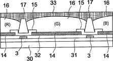
With reference to the description of drawings embodiments of the invention.Express to Fig. 1 pattern the circuit diagram of pixel portion of the present invention.Fig. 2 is the planimetric map of the pixel periphery of display device.Fig. 3 be the light-emitting component that in pixel, is provided with analyse and observe skeleton diagram (the D-D section of Fig. 2).Light-emitting component has used organic EL 1 among this embodiment.In addition, comparative electrode 33 shown in Figure 3 omits in Fig. 2 in order to understand drawing easily.
As shown in Figure 1, organic EL 1 flows to comparative electrode 33 and luminous by electric current from pixel electrode 14, can adjust brightness by controlling this current value.For the organic EL 1 that makes certain specific pixel luminous, by make sweep signal flow through signal line 2, data-signal flows through source signal line 3, thereby, supply with sweep signal to grid 13 to supplying with data-signal with the source electrode 11 of TFT6 in conduct the 2nd transistorized control of seeing the part configuration that two signal wires intersect from the plane.Like this, when control is connected with TFT6, grid 10 is connected to control with the connecting with TFT5 as the 1st transistorized driving of the drain electrode 12 of TFT6, by driving with the source electrode 8 of TFT5 and draining 9, makes organic EL luminous the current supply organic EL from electric power supply line 4.Have maintenance electric capacity 34 in control with TFT6 with between driving with TFT5, keep an electrode of electric capacity 34 to be formed by electric power supply line 4, another electrode is by forming with drain electrode 12 auxiliary electrodes that form simultaneously.And, even becoming electronegative potential, sweep signal controls disconnection with TFT6, the grid potential that drives with TFT5 also keeps official hours, the luminous continuation of organic EL 1 by maintenance electric capacity 34.
The structure of display device of the present invention then, is described with reference to Fig. 2, Fig. 3.In the viewing area, signal line 2 is become rectangular with source signal line 3 distributions, form pixel in the part of surrounding by signal line 2 and source signal line 3.Be arranged on the organic EL 1 that luminescent layer 16 has used organic EL in each pixel, forming respectively will be from the driving of this organic EL 1 of current supply of electric power supply line 4 with TFT5 and the controlling and driving control TFT6 with the on/off of TFT5.And when from electric power supply line 4 during to organic EL 1 supplying electric current, luminescent layer 16 carries out luminous with shades of colour, can adjust brightness by the Control current value.
On glass substrate 30, make a plurality of signal line 2 parallel distributions, along 3 electric power supply lines 4 of signal line 2 distributions.Signal line 2 and electric power supply line 4 all form in same operation simultaneously, are formed by Al or Cr.Article 3, electric power supply line 4 corresponds respectively to R, G, the B of pixel and is provided with, R is connected with the organic EL 1 with red luminescent layer 16 (R) with electric power supply line 4R, G is connected with the organic EL 1 with green luminescent layer 16 (G) with electric power supply line 4G, and B is connected with the organic EL 1 of electric power supply line 4 with the luminescent layer 16 (B) with blue look.The color difference that organic EL 1 sends owing to luminescent material, meanwhile its luminescence efficiency is also different, so at each color electric power supply line 4 is set, is suitable for versicolor electric current by supply, can carry out optimal panchromatic demonstration.
When forming signal line 2 and electric power supply line 4, between electric power supply line 4 and organic EL 1, form the grid 10 that drives with TFT5 simultaneously.This grid 10 forms horizontal long shape along electric power supply line 4, and the minor face of one side is a linearity, and the opposing party's minor face is circular-arc.Driving in order to realize the function with the current supply organic EL, must be flow through big as far as possible electric current with TFT5 when connecting, therefore the grid 10 that drives with TFT5 forms as wide as possible.
Stacked by SIN on glass substrate 30
XThe gate insulating film 31 that (silicon nitride film) constitutes is by this gate insulating film 31 cover gate signal wires 2 and electric power supply line 4.On gate insulating film 31, be laminated with amorphous silicon layer (hereinafter referred to as the a-Si layer), with the only residual part of photoetching process corresponding to TFT5,6 semiconductor layer (active layer) 7,13.At this moment the a-Si layer 7 that drives with TFT5 forms along the shape of the outer rim of grid 10, is layered on the major part of grid 10, and a part is outstanding from the short leg and the arc sections of grid 10.And control forms the square shape of crossing over signal line 2 with the a-Si layer 13 of TFT6.
The metal level that has formed Al and Mo on a-Si layer 7,13 and gate insulating film 31 stacked makes this metal level form figure with photoetching process, forms source signal line 3 and TFT5,6 source-drain electrode etc.At this moment source signal line 3 and signal line 2 are provided with orthogonally, from source signal line 3 and the portion of reporting to the leadship after accomplishing a task of signal line 2 near outstandingly extend to control with the source electrode 11 on the a-Si layer 13 of TFT6.Control is connected with the grid 10 that drives with TFT5 with transparency electrode 21 described later by auxiliary electrode 134 with the drain electrode 12 of TFT6, and the electric current that will flow through source signal line 3 when control is connected with TFT6 offers the grid 10 that drives with TFT5.With auxiliary electrode 134 that control is connected with the drain electrode 12 of TFT6 gate insulating film 31 is clipped in the middle and covers electric power supply line 4, form maintenance electric capacity 34 by electric power supply line 4 and auxiliary electrode 134.Particularly under the situation of a-Si type TFT, to compare gate insulating film 31 thick with polysilicon type TFT, so keep the electric capacity of electric capacity 34 to diminish.Therefore in order to replenish its electric capacity deficiency, preferably make the part broadness that covers electric power supply line 4 by auxiliary electrode 134 as far as possible, cover the major part of the electric power supply line 4 in the pixel with auxiliary electrode 134.
In driving, forming the source electrode 8 of U font roughly and be positioned at the drain electrode 9 of the roughly linearity of two of this source electrode 8 between pitching with TFT5.The peripheral edge portion relative with drain electrode 9 is outstanding and extend near the electric power supply line 4 electrode 8a never forming on this source electrode 8, is connected with electric power supply line 4 corresponding to each pixel color by transparency electrode 19 described later.And, be formed with bent and extend to the electrode 9a of the pixel electrode 14 of organic EL 1 to organic EL 1 lateral bending in drain electrode 9, and be electrically connected with pixel electrode 14 from the outstanding part of a-Si layer 7.
Driving forms along the shape of the outer rim of grid 10 with the outer rim of the source electrode 8 of TFT5, and two forks of U font are divided long as far as possible on grid 10, and drain electrode 9 also slenderly forms corresponding to the shapes that two forks of source electrode 8 are divided.Driving with TFT5 because must be to the electric current of pixel electrode 14 supply capability supply lines 4, so electric current is flowed.A-Si type TFT compares with the polysilicon type, and it is more difficult that electric current flows, so when driving with TFT5 use a-Si type TFT, must make this driving big as far as possible with TFT5.That is, flow easily in order to make electric current, can make passage length shorter, make channel width bigger, passage length is less to have boundary aspect manufacturing technology but make, so effective method is to make driving make channel width big as much as possible greatly with TFT5.Therefore, in this embodiment the shape of source-drain electrode 8,9 is tried every possible means, electric current is flowed by driving with TFT5.That is, by making the grid 10 that drives with TFT5 laterally longer, source electrode 8 and drain electrode 9 are elongated, can make channel width bigger in the space that limits.Especially by the laterally long grid 10 of configuration, make it vertically parallel with signal line 2, can spread all between the adjacent source signal line 3 and form to drive and use TFT5, by making its channel width direction parallel, can in the limited size that drives with TFT5, increase channel width effectively again with signal line 2.And then by making source electrode 8 become the U font, and configuration drain electrode 9 between two forks of U font, because source electrode 8 is positioned at the both sides of drain electrode 9, channel width becomes 2 times, so can make channel width become big in little space effectively.
Since control with TFT6 only controlling and driving get final product with the on/off of TFT, use TFT5 different with driving, mobile electric current is less to get final product, it is less that only this just can make its size.If make control less with TFT6, then can therefore guarantee the space of configuration driven with TFT5, can make driving become big with TFT5.Therefore, see near signal line 2 and source signal line 3 intersections, make the distribution branch of source signal line 3, use the source electrode 11 of TFT6 to use as control the fore-end of this branch from the plane.And, as described later, by with source signal line 3 and this component, be that source electrode 11 sees that from solid distribution is above signal line 2, again by control with the drain electrode 12 of TFT6 also be formed on simultaneously with source electrode 11 in textural identical stratum, thereby produce the advantage of the grid 13 that signal line 2 can be also used as control usefulness TFT6.
At control TFT6, source electrode 11 and drain electrode 12 are on a-Si layer 13, only mutual one side is relative, but at driving TFT5, owing to dispose source electrode 8 with the form of surrounding drain electrode 9, so its channel width change is big, in addition, in this embodiment, owing to be channel width 3 times or more of control with TFT6 with the length that drives with the relative drain electrode 9 of the source electrode 8 of TFT5, so the channel width that drives with TFT5 then is to control more than 6 times of channel width of using TFT6.So as if guaranteeing to make the channel width that drives with TFT5 to increase, even then under situation about driving, also can realize optimum demonstration with TFT use a-Si type TFT.Also have, in this embodiment, owing to make driving big as much as possible, so drive 6 times of channel width that channel width with TFT5 is control usefulness TFT6 with TFT5, but if make the channel width that drives with TFT5 is channel width 4 times or more of control with TFT6, just can obtain high-grade demonstration.In this embodiment, with control with TFT6 and drive set for the passage length of TFT5 roughly the same, but if make the passage length that drives with TFT5 littler with the passage length of TFT6, then so and electric current is mobile easily than control.
Formation is by SiN
XThe dielectric film 32 that constitutes makes it cover source signal line 3 and TFT5,6, the stacked transparency electrode that is made of ITO (tin indium oxide) or IZO (cupric oxide zinc) on dielectric film 32.Make this transparency electrode form figure with photoetching process, thereby form pixel electrode 14.This pixel electrode 14 is positioned at each pixel and becomes roughly ellipticity, and along 3 configurations of source signal line, its part is outstanding, and is overlapping with a part that drives the drain electrode 9a that uses TFT5.In this pixel electrode 14 and the overlapping part of drain electrode 9a, on the dielectric film 32 on the drain electrode 9a, form contact hole 23, pixel electrode 14 is electrically connected with drain electrode 9a by contact hole 23.
When forming pixel electrode 14, transparency electrode also remains in electric power supply line 4 and drives with between the source electrode 8a of TFT5, and electric power supply line 4 and source electrode 8a are electrically connected.Promptly, on electric power supply line 4 corresponding to pixel, on gate insulating film 31 and dielectric film 32, form contact hole 18a, make the part of electric power supply line 4 expose, driving with above the source electrode 8a of TFT5, form contact hole 18b on dielectric film 32, make the part of source electrode 8a expose, transparency electrode 19 contacts with the electric power supply line 4 that exposes at two contact hole 18a, 18b, source electrode 8a.
And transparency electrode also remains in auxiliary electrode 134 and drives with between the source electrode 10 of TFT5, and transparency electrode 21 contacts with the auxiliary electrode 134 that exposes at two contact hole 20a, 20b, grid 10, is electrically connected two electrodes 10,134.
Then, represent the planimetric map of 1 pixel in 3 pixels of RGB shown in Figure 2 at Fig. 4, and explanation respectively want portion layer section.Fig. 5 is the general profile chart (the A-A section of Fig. 4) of control with the TFT6 periphery.At first, as display device, on shared glass substrate 30, form signal line 2.Form the gate insulating film 31 that constitutes by SiNx thereon, so also by 31 while of gate insulating film cover gate signal wire 2.On gate insulating film 31, a-Si layer 13 is above it stacked with the form of crossing over signal line 2.By containing the N type a-Si film 13a of N type impurity, the metal level that has formed Al and Mo stacked makes this metal level form figure by photoetching process on a-Si layer 13, forms source signal line 3, the source electrode 11 from source signal line 3 branches, drain electrode 12.The stacked respectively thereon dielectric film 32 that constitutes by SiNx, by SiO
2The diaphragm 15 that (monox) constitutes, bank (バ Application Network) layer 17, comparative electrode 33.
As described above, article 3, electric power supply line 4 is corresponding with R, G, the B of pixel respectively and be provided with, even but 3 the electric power supply lines 4 that connect up like this, electric power is supplied with 4 with respect to gate signal line 2 row wirings, the feasible area that can give organic EL 1 does not reduce yet, simultaneously keep electric capacity 34 and do not append new maintenance electric capacity line and plane domain in order to form, utilize electric power supply line 4 at an upper portion thereof solid be provided with and keep electric capacity 34.Usually keep electric capacity 34 in order to form, as signal line 2 and source signal line 3, connecting up with the form that connects each pixel keeps the electric capacity line, but present embodiment does not have the sort of necessity.
With reference to the electric power supply line of Fig. 6 and the general profile chart (the B-B section of Fig. 4) of maintenance electric capacity periphery, the concrete structural map of this electric power supply line 4 and maintenance electric capacity 34 is described.At first, as display device, on the identical layer of signal line on the shared glass substrate 30 and shown in Figure 52, form respectively B with electric power supply line 4B, G with electric power supply line 4G, R with electric power supply line 4R, realize keeping the function of an electrode of electric capacity 34 simultaneously.Thereon owing to forming the gate insulating film 31 that constitutes by SiNx, so cover 3 electric power supply lines 4 simultaneously by gate insulating film 31.And, the metal level that on the identical layer of the electrode of source electrode on the gate insulating film 31 and shown in Figure 5 11 and drain electrode 12, has formed Al and Mo stacked, make this metal level form figure with photoetching process, prolong drain electrode 12 shown in Figure 5 and another auxiliary electrode 134 of formation maintenance electric capacity 34.Electric power supply line 4 that forms like this and maintenance electric capacity 34 constitute maintenance electric capacity 34a, 34b, the 34c (Fig. 1) that each color pixel needs particularly.
Keep electric capacity 34 that its auxiliary electrode 134 is connected with the grid 10 (Fig. 2) that drives with TFT5.Promptly, on the dielectric film 32 on the auxiliary electrode 134 that keeps electric capacity 34, form contact hole 20a, make the part of auxiliary electrode 134 expose, and then as shown in Figure 2, on the part of gate insulating film 31 and dielectric film 32, also form contact hole 20b, make driving expose with the part of the grid 10 of TFT5.And, forming the transparency electrode 21 that constitutes by ITO or IZO with the form of crossing over two contact hole 20a, 20b, auxiliary electrode 134 that exposes from contact hole 20a and the grid 10 that exposes from contact hole 20b are electrically connected by transparency electrode 21.Distinguish stacked guard film 15, bank layer 17, comparative electrode 33 thereon on the surface layer.
The structure of driving usefulness TFT5 then, is shown with the general profile chart (the C-C section of Fig. 4) of TFT periphery in the driving of Fig. 7.At first, on shared glass substrate 30, form grid 10 as display device.Form the gate insulating film 31 that constitutes by SiNx thereon, so by 31 while of gate insulating film cover gate 10.The further stacked semiconductor layer that constitutes by a-Si layer 7 on gate insulating film 31.On this a-Si layer 7, by containing the N type a-Si film 7a of N type impurity, the metal level that has formed Al and Mo stacked makes this metal level form figure with photoetching process, forms source electrode 8 and drain electrode 9 electrodes that constitute by the U font respectively.And then, form the dielectric film 32 that constitutes by SiNx thereon.
By each element and the wiring of above-mentioned such formation, drive organic EL 1 and luminous, with reference to Fig. 3 its structure is described.The 15th, by SiO
2The diaphragm that constitutes forms on dielectric film 32, overlaps the peripheral part of the pixel electrode 14 of organic EL 1.That is, diaphragm 15 covers the peripheral part of pixel electrodes 14, but the major part that comprises pixel electrode 14 middle bodies is removed.The 17th, the bank layer that is made of novolac resin that forms on diaphragm 15 forms thicklyer than diaphragm 15 and dielectric film 32.In with these bank layer 17 area surrounded, apply organic EL, thereby form bank layer with the form of surrounding pixel electrode 14 along the outer rim of pixel electrode 14 as luminescent material.If only stockpile luminescent material, then bank layer 17 be arranged on pixel electrode 14 around get final product, but also be arranged on two TFT5 in this embodiment, 6 and electric power supply line 4 on.Bank layer 17 also can form with organic resin beyond the novolac resin or inorganic resin so long as insulator gets final product.
On pixel electrode 14, apply the luminescent material corresponding, and accumulate in by in bank layer 17 area surrounded with each color of pixel with ink-jetting style.This luminescent material uses organic EL, for example uses the conjugated polymer presoma.Then, make the luminescent material producing high-molecular, each pixel is formed the luminescent layer 16 of R, G, B with heat treated.
The 33rd, by the comparative electrode that Al and Cr constitute, be layered on the luminescent layer 16.Comparative electrode 33 is formed on whole viewing area, supplies with the voltage of regulation.If constitute this comparative electrode 33 with metal level, can produce luminous by luminescent layer 16, so also can form comparative electrode 33 with the metal beyond Al and the Cr, but if as this embodiment, constitute comparative electrode 33 with Al and the such high metal level of light reflectivity of Cr, then can be effectively in the future the light of spontaneous photosphere 16 be used in demonstration, can realize the more demonstration of high brightness.During electric current more than pixel electrode 14 is supplied with threshold values, luminescent layer 16 is luminous, can observe this light from glass substrate 30 sides.
For example, the electric power supply line 4 supply+10V (Vdd (B)) that use as the electric power supply line 4 supply+8V that use to R, G (Vdd (R), Vdd (G)), to B, during to comparative electrode 33 supply-3V, when to signal line 2 output scanning signals, to source signal line 3 supply data-signals, the control of scanning is connected with TFT6, at this moment the data-signal that flows through source signal line 3 supplies to the grid 10 that drives with TFT5 by the drain electrode of controlling with TFT6 12, drives and connects with TFT5.Then, even control disconnects with TFT6, owing to, supply to pixel electrode 14 by driving with TFT5 so flow through the electric current of corresponding electric power supply line 4 by keeping electric capacity 34 to keep the on-state that drives with TFT5.And in the potential difference (PD) that produces between pixel electrode 14 and the comparative electrode 33 more than the regulation, electric current flows in luminescent layer 16, sends the light corresponding to the color of luminescent material.In addition, at organic EL, the luminescence efficiency of blue look luminescent material is poorer than the luminescence efficiency of the luminescent material of other colors, so the voltage higher than the pixel electrode 14 of other pixels will be provided to the pixel electrode 14 of the pixel of blue look.
In the present invention, make luminescent layer 16 for vertical long shape and with source signal line 3 configured in parallel, make to drive to be horizontal long shape and to be configured to parallel with signal line 2 with TFT5.That is, configuration driven TFT5, the feasible vertical quadrature that drives with the vertical and luminescent layer 16 of TFT5.According to this configuration, in the limited area of surrounding, can in the big luminescent layer 16 of configuration, make driving big as much as possible with TFT5 with source signal line 3 and signal line 2.Especially can with drive with TFT5 be set to source signal line 3 near, can spread all over area configurations between the adjacent source signal line 3 and drive and use TFT5, so can make driving bigger with TFT5.Therefore, be a-Si type TFT even make driving with TFT5, also can provide sufficient electric current to luminescent layer 16, can obtain best demonstration.
Here, the driving that makes horizontal long shape dispose with the vertical luminescent layer 16 of long shape orthogonally with TFT5, is in order to make sufficient electric current mobile with driving with TFT5, that is, the channel width change greatly.Thereby, form elongated passage with TFT5 driving, vertical quadrature of (passage vertically) and luminescent layer 16 then can increase width of channel effectively in limited zone if the direction of this channel width.
In the present invention, in by signal line 2 and source signal line 3 area surrounded, use the series arrangement of TFT6 with TFT5,3 electric power supply lines 4, controls with luminescent layer 16, driving along source signal line 3.According to this configuration, can each arrangements of components is neat, can dwindle the configuration area of light-emitting component element in addition, simultaneously the current circuit length from the electric power supply line to light-emitting component is shortened.In addition, driving with TFT5 and control configuration electric power supply line 4 between the TFT6, because this electric power supply line 4 is also used as the maintenance electric capacity 34 that drives with TFT5,, many electric power supply lines 4 corresponding with each luminescent layer 16 can be set so can effectively use the space in the pixel.
Stacked so various layers and the pixel that forms have the gate insulating film 31, dielectric film 32, transparency electrode 21, diaphragm 15, bank layer 17 of a plurality of as Fig. 5~shown in Figure 7 or pixel electrode 14 shown in Figure 3 etc. approaching transparent layer.Again, from aforesaid explanation as can be known, owing to make the regional little of configuration element of relevant controlling and wiring and make light-emitting zone big as far as possible as far as possible, so control is configured near the luminescent layer 16 of neighbor with TFT6, and drive with TFT5 and be configured near the luminescent layer 16 in the pixel, particularly driving with TFT5 has big channel width, with respect to luminescent layer 16 configured in parallel.Thus, just incide the semiconductor layer of these TFT easily from the light of luminescent layer 16, but produce the light leakage at TFT when incident, predetermined electric current can not be supplied with light-emitting component.Therefore, actual show state is with different corresponding to the show state of the shows signal that will reproduce, and display level is low.
With reference to Fig. 8 A, Fig. 8 B, the shading from the light of luminescent layer 16 is described.Fig. 8 A be when representing not shading to the view of TFT incident light, the view of the light path when Fig. 8 B is the expression shading.For convenience of explanation, only diagram is main layer, and other layers omit.In Fig. 8 A, the light transmission bank layer 17 that sends from the luminescent layer 16 that covers comparative electrode 33 incides driving with the not shown semiconductor active layer of TFT5.At this moment the light from luminescent layer 16 comprises the light of the side that is directly incident on the semiconductor active layer and reflects the light of back incidents above the semiconductor active layer by comparative electrode 33.Also incide simultaneously the not shown semiconductor active layer of control with TFT6.Particularly a-Si also can be used as semiconductor and is subjected to the influence of light easily, produces big leakage current by rayed.
Therefore, shown in Fig. 8 B, with the bank layer between the TFT5 17 notch 35 is set at luminescent layer 16 and driving.With the bank layer between the TFT6 same notch 36 is set also at luminescent layer 16 and driving again.Then, form from top covering comparative electrode 33.Comparative electrode 33 is so catoptrical metal levels such as Al or Cr as described above, by covering the inner face of the comparative electrode 33 that notch 35 and 36 forms, makes light not incide TFT and is reflected.
At this moment, the interior shape of the comparative electrode 33 by notch 35,36 reflects light to the downside of figure, when being not shown glass substrate direction, has improved from the glass substrate side and has watched being seen brightness when showing.The shape of notch 35,36, be the profile that makes the luminescent layer side shape along the profile of luminescent layer 16, the light of spontaneous photosphere 16 is used for showing expeditiously more in the future, and the profile of TFT side is positioned near the TFT as far as possible, then more can prevent the incident of light to TFT reliably.
As shown in Figure 2, be provided with at luminescent layer 16 on the Width of pixel point-blank and driving, but be almost along the such shape of outer rim of luminescent layer 16 Widths with the notch 36 between the TFT6 in luminescent layer 16 and control with the notch 35 between the TFT5.That is, owing to be a-Si type TFT, the Width that spreads all over pixel forms significantly with TFT5 in driving, makes to supply with sufficient electric current to pixel electrode 14, in order to prevent to this driving TFT5 incident light, form notch 35 along driving more longways with TFT5.Owing to control the cross part that is formed on signal line 2 and source signal line 3 with TFT6, so notch 36 is formed near the cross part of two signal wires 2,3 at least.And, between two signal wires, 2,3 cross parts, also forming notch 36, can reliably prevent from the light of luminescent layer 16 can be directed to the viewing area of below simultaneously to control TFT6 irradiates light.If like this, then can carry out shading to not light with the form that covers light source from luminescent layer 16, make by the original light path of the light of notch 36 reflections and luminescent layer 16 overlappingly simultaneously, can further improve brightness.
Influence from the light of luminescent layer 16 does not rest in the same pixel, and also influential driving to neighbor is with the possibility of TFT, and, improving the viewpoint of reflection efficiency from notch, notch 35,36 is preferably the length approaching with the minor face of pixel.
Form comparative electrode 33 covering on two TFT5,6 the bank layer 17.That is, cover two TFT5,6 top, can prevent light incident from two TFT5,6 top by comparative electrode 33 with light-proofness.The electric conductors such with comparative electrode 33 cover TFT5,6 above situation under, bank layer 17 also realizes expanding TFT5,6 and the function at the interval of comparative electrode 33.In order to be configured in comparative electrode 33 near TFT5,6 position, TFT5,6 action are caused bad influence at the additional certain voltages usually of comparative electrode 33.Thereby, TFT5,6 and comparative electrode 33 preferably separate as far as possible, can guarantee that by making the thickness thickening that covers TFT5,6 bank layer 17 it is at interval.Thereby, even around light-emitting component, do not form under the situation of bank layer 17, by bank layer 17 is set, stacked comparative electrode 33 on this bank layer 17 on TFT5,6, can prevent also that to TFT5,6 incident lights it is effective that bank layer 17 is set on TFT5,6.At this moment, because bank layer 17 is set, make the ora terminalis of bank layer 17 between light-emitting component and TFT5,6, also can form the structure that notch 35,36 is not set.
In this embodiment, form the film of light-proofness of the top of the notch be positioned at bank layer and TFT with comparative electrode.Thereby, do not need to form the film of the light-proofness beyond the comparative electrode, so manufacturing process is simple.Yet the present invention is not limited to form with comparative electrode the film of this light-proofness, for example, also can form the resin molding of black on the bank layer that covers TFT.
As described above, the objective of the invention is therefore to there is no need to make polysilicon type TFT,, can obtain cheap display device so manufacturing process is simple with the TFT of a-Si type TFT formation to the organic EL supplying electric current.And, so long as in the scope that does not break away from aim of the present invention, also can be the form beyond the foregoing description.For example, in this embodiment, use TFT5 as driving, used drain electrode 9, surrounded the TFT of the source electrode 8 of the such U font of drain electrode 9 with linearity, formed the structure that has the passage area of elongate in the two sides of drain electrode 9, if but can supply with the structure of abundant electric current to organic EL, then will not drive and be limited to this form with TFT, for example, also can be the form of such source of configuration, drain electrode: have the source electrode and the drain electrode of horizontal long shape respectively, vertical quadrature of its channel width direction and luminescent layer 16.And the source, the drain electrode that drive with TFT5 also can form other shapes, also source electrode can be formed the コ font and drain electrode is formed linearity, perhaps drain electrode is formed the U font and source electrode is formed linearity.
Use the TFT of the a-Si type TFT formation of n channel-style in the present invention, but also can use the a-Si of p channel-style to the organic EL supplying electric current.That is, owing to form TFT with the passage of same kind, manufacturing process is simple, can obtain cheap demonstration equipment.
Utilizability on the industry
The present invention is in a plurality of pixel arrangement being become rectangular display unit, has in each pixel and establishes The light-emitting component of vertical long shape of putting, in each pixel, arrange simultaneously and supply with electric current to above-mentioned light-emitting component And make its luminous driving drive the control TFT with the action of TFT with TFT, control, drive and use TFT forms horizontal long shape so that its vertically and the mode of vertical quadrature of light-emitting component adjacent to above-mentioned The minor face of light-emitting component and disposing makes that to drive with TFT and the semiconductor layer controlled with TFT be a-Si. Cause This even use in the situation of a-Si type TFT, can make driving as much as possible big with TFT, energy Enough supply with sufficient electric current to light-emitting component. And, do not need the manufacturing of high manufacturing technology and high price to fill Put, because can be with the uniform TFT of large tracts of land manufacturing characteristics, so low price, also suitable large-scale can be provided The display unit of the emissive type of changing.
In addition, by pressing light-emitting component along the source signal line, driving with TFT, electric power supply line, control System is configured with the order of TFT, can effectively dispose each element in the confined space in pixel, Light-emitting component can be configured to bigger the time, make to drive greatlyyer with TFT, therefore obtain good aobvious The display unit of showing state.
Form elongate by the passage area that will drive with TFT, with the electricity of the side in source, the drain electrode The utmost point forms roughly linearity, and the opposing party's electrode forms the shape of the electrode that surrounds a side, thus energy Increase to drive the channel width with TFT, namely using also can be to light-emitting component in the situation of a-Si type TFT Supply with sufficient electric current.
By being parallel to above-mentioned grid driving with TFT and be provided with length direction between controlling with TFT The maintenance electric capacity of holding wire keeps a side's of electric capacity electrode to be also used as the electric power supply line, the opposing party's electricity The utmost point uses the auxiliary electrode of the grid of TFT to form by connecting control with the drain electrode of TFT and driving, thereby not Need to form the special-purpose electric capacity line that keeps electric capacity to use, each arrangements of components can be got closely, expansion can be distributed to The area of light-emitting component is being made contributions aspect raising luminous efficiency and the brightness.
By many electric power supply lines corresponding to each glow color of light-emitting component are set, driving usefulness Thin film transistor (TFT) and control supply to light-emitting component with these many electric power supply lines of configuration between the thin film transistor (TFT) Give the electric current of self-corresponding electric power supply line, be suitable for the different shades of colour of luminous efficiency thereby supply with The electric current of light-emitting component, can carry out optimal panchromatic demonstration thus.
Use the signal line as control with the grid of TFT, formation control is used on the signal line TFT, thus also passable even grid is not set especially since do not need formation control with TFT use new The zone, can guarantee significantly that thus configuration driven is with the space of TFT.
Formation is configured in the bank layer around the light-emitting component, make its also with drive with TFT and control TFT Overlapping, the control that further arranges in the pixel with TFT and adjacency at light-emitting component and driving is used Form notch on the bank layer between the TFT, at least stacked light-proofness near the bank layer the notch Film, can reduce thus light from luminescent layer and incide the light that causes in the semiconductor layer of these TFT and let out Leak, can provide display level high display unit.
And, use TFT by form driving with any the a-Si in n channel-style or the p channel-style Use TFT with control, thereby manufacturing process is oversimplified, also do not need the manufacturing equipment of complexity, can Realize this reduction when improving yield rate.
Claims (16)
1. a display device becomes rectangular with a plurality of pixel arrangement, it is characterized in that having: the vertical light-emitting component of long shape is arranged in each pixel; Drive and use thin film transistor (TFT), be arranged in each pixel, and make it luminous to above-mentioned light-emitting component supplying electric current; The control thin film transistor (TFT), control the action of above-mentioned driving with thin film transistor (TFT), above-mentioned driving forms horizontal long shape with thin film transistor (TFT), mode with the length direction quadrature of its length direction and above-mentioned light-emitting component disposes adjacent to the minor face of above-mentioned light-emitting component, and above-mentioned driving is formed by amorphous silicon with thin film transistor (TFT) and the control semiconductor layer with thin film transistor (TFT).
2. display device as claimed in claim 1, it is characterized in that, make light-emitting component form vertical long shape, make above-mentioned driving form horizontal long shape with thin film transistor (TFT), be configured to rectangular with being connected in the signal line and the source signal line of above-mentioned control with thin film transistor (TFT), above-mentioned light-emitting component is configured to its length direction and above-mentioned source signal line parallel, above-mentioned driving is configured to its length direction and above-mentioned signal line parallel with thin film transistor (TFT).
3. display device as claimed in claim 2 is characterized in that, above-mentioned driving thin film transistor (TFT) is configuration like this: make passage area form elongate, the length direction of this passage area and above-mentioned signal line parallel.
4. display device as claimed in claim 1 is characterized in that, above-mentioned driving thin film transistor (TFT) is that an electrode in source electrode and the drain electrode is formed linearity, another electrode is formed the shape that surrounds an electrode.
5. display device as claimed in claim 1 is characterized in that, above-mentioned driving have the source electrode of U font with thin film transistor (TFT) and be configured in above-mentioned U font two the fork between drain electrode.
6. display device as claimed in claim 1, it is characterized in that, in every row, has the signal line that is being connected with the grid common land of thin film transistor (TFT) with the above-mentioned control that in each pixel of row matrix direction, is provided with, be configured with being parallel to this signal line and by above-mentioned driving with the electric power supply line of thin film transistor (TFT) to above-mentioned light-emitting component supplying electric current, in every row, have with the above-mentioned control that in each pixel of column direction, is provided with and be connected with the source electrode common land of thin film transistor (TFT), and the source signal line that intersects with above-mentioned signal line, in by above-mentioned signal line and above-mentioned source signal line area surrounded, from the plane, press light-emitting component along the source signal line, drive and use thin film transistor (TFT), the electric power supply line, control is configured with the order of thin film transistor (TFT).
7. display device as claimed in claim 6, it is characterized in that, be provided with maintenance electric capacity that length direction be parallel to above-mentioned signal line with thin film transistor (TFT) and above-mentioned control between with thin film transistor (TFT) in above-mentioned driving, an electrode of above-mentioned maintenance electric capacity is also used as the electric power supply line, another electrode is by forming with the auxiliary electrode that the drain electrode of thin film transistor (TFT) is connected with above-mentioned control, and above-mentioned auxiliary electrode is electrically connected on the grid of above-mentioned driving with thin film transistor (TFT).
8. display device as claimed in claim 6, it is characterized in that, has the light-emitting component that sends different colours, many the electric power supply lines corresponding with each glow color are set, should many electric power supply lines be configured in and drive with thin film transistor (TFT) and control with between the thin film transistor (TFT), supply with the electric current of self-corresponding electric power supply line to light-emitting component.
9. display device as claimed in claim 6 is characterized in that, as the grid use signal line of above-mentioned control with thin film transistor (TFT), above-mentioned control is formed on the signal line with thin film transistor (TFT).
10. display device as claimed in claim 1, it is characterized in that, around above-mentioned light-emitting component, dispose bank layer, above-mentioned bank layer forms with the form on the thin film transistor (TFT) also to overlap above-mentioned driving, be formed with notch in above-mentioned light-emitting component and above-mentioned driving on the above-mentioned bank layer between the thin film transistor (TFT), near the above-mentioned bank layer the notch, be laminated with the film of light-proofness at least.
11. display device as claimed in claim 1, it is characterized in that, around above-mentioned light-emitting component, dispose bank layer, above-mentioned bank layer forms with the form on the thin film transistor (TFT) also to overlap above-mentioned control, at above-mentioned light-emitting component be arranged at above-mentioned control on the adjacent pixels and be formed with notch on the above-mentioned bank layer between the thin film transistor (TFT), near the above-mentioned bank layer the notch, be laminated with the film of light-proofness at least.
12. display device as claimed in claim 1, it is characterized in that, use the form of thin film transistor (TFT) to form bank layer to cover above-mentioned driving with thin film transistor (TFT) and above-mentioned control, the ora terminalis of above-mentioned bank layer is driving with thin film transistor (TFT) and between controlling with thin film transistor (TFT) and above-mentioned light-emitting component, is being laminated with the film of light-proofness on above-mentioned bank layer.
13. as each described display device in the claim 10~12, it is characterized in that having: pixel electrode is configured in the below of the luminescent layer of above-mentioned light-emitting component, and is connected with thin film transistor (TFT) with above-mentioned driving; Comparative electrode across above-mentioned luminescent layer and dispose relative with pixel electrodes, and covers above-mentioned bank layer, and the film of above-mentioned light-proofness is formed by above-mentioned comparative electrode.
14., it is characterized in that above-mentioned driving is formed by the n channel-style with thin film transistor (TFT) with thin film transistor (TFT) and above-mentioned control as each described display device in the claim 1~12.
15., it is characterized in that above-mentioned driving is formed by the p channel-style with thin film transistor (TFT) with thin film transistor (TFT) and above-mentioned control as each described display device in the claim 1~12.
16., it is characterized in that above-mentioned light-emitting component is an organic field luminescence as each described display device in the claim 1~12.
Applications Claiming Priority (8)
| Application Number | Priority Date | Filing Date | Title |
|---|---|---|---|
| JP2002125592 | 2002-04-26 | ||
| JP125592/2002 | 2002-04-26 | ||
| JP2002159124 | 2002-05-31 | ||
| JP159124/2002 | 2002-05-31 | ||
| JP2002173817 | 2002-06-14 | ||
| JP173817/2002 | 2002-06-14 | ||
| JP2002173816 | 2002-06-14 | ||
| JP173816/2002 | 2002-06-14 |
Publications (2)
| Publication Number | Publication Date |
|---|---|
| CN1628333A CN1628333A (en) | 2005-06-15 |
| CN1297948C true CN1297948C (en) | 2007-01-31 |
Family
ID=29273739
Family Applications (1)
| Application Number | Title | Priority Date | Filing Date |
|---|---|---|---|
| CNB038033518A Expired - Lifetime CN1297948C (en) | 2002-04-26 | 2003-04-23 | Display device |
Country Status (7)
| Country | Link |
|---|---|
| US (2) | US7488972B2 (en) |
| EP (1) | EP1501067B1 (en) |
| JP (1) | JP4053040B2 (en) |
| KR (1) | KR100775205B1 (en) |
| CN (1) | CN1297948C (en) |
| TW (1) | TW586095B (en) |
| WO (1) | WO2003091971A1 (en) |
Families Citing this family (22)
| Publication number | Priority date | Publication date | Assignee | Title |
|---|---|---|---|---|
| US7488972B2 (en) * | 2002-04-26 | 2009-02-10 | Sanyo Electric Co., Ltd. | Organic luminescent display device having a semiconductor with an amorphous silicon layer |
| KR101061882B1 (en) * | 2002-09-11 | 2011-09-02 | 가부시키가이샤 한도오따이 에네루기 켄큐쇼 | Light emitting device and manufacturing method thereof |
| JP2006259530A (en) * | 2005-03-18 | 2006-09-28 | Seiko Epson Corp | Organic el device, driving method thereof, and electronic device |
| US7511257B2 (en) * | 2005-08-24 | 2009-03-31 | Aptina Imaging Corporation | Method and apparatus providing and optical guide in image sensor devices |
| KR101350609B1 (en) * | 2005-12-30 | 2014-01-10 | 엘지디스플레이 주식회사 | Thin film transistor array substrate and manufacturing method of the same |
| US7867088B2 (en) * | 2006-05-23 | 2011-01-11 | Mga Entertainment, Inc. | Interactive game system using game data encoded within a video signal |
| CN101082746B (en) * | 2006-05-31 | 2013-03-20 | 株式会社日立显示器 | Display device |
| JP5392545B2 (en) * | 2009-03-13 | 2014-01-22 | ソニー株式会社 | Display device |
| JP5312294B2 (en) * | 2009-10-30 | 2013-10-09 | キヤノン株式会社 | Light emitting apparatus and exposure apparatus |
| WO2011070929A1 (en) | 2009-12-11 | 2011-06-16 | Semiconductor Energy Laboratory Co., Ltd. | Semiconductor device and electronic device |
| JP5468133B2 (en) * | 2010-05-14 | 2014-04-09 | パナソニック株式会社 | Solid-state imaging device |
| JP2012018386A (en) * | 2010-06-08 | 2012-01-26 | Canon Inc | Display device and driving method |
| FR2976127B1 (en) * | 2011-06-01 | 2014-01-10 | Commissariat Energie Atomique | ORGANIC ELECTRODE COMPONENT HAVING IMPROVED ARRANGEMENT AND SHAPE |
| KR20140052730A (en) * | 2012-10-25 | 2014-05-07 | 삼성디스플레이 주식회사 | Organic light emitting display device, method of authenticating using the same and identification comprising organic light emitting display device |
| US10006910B2 (en) | 2014-12-18 | 2018-06-26 | Agilome, Inc. | Chemically-sensitive field effect transistors, systems, and methods for manufacturing and using the same |
| US11921112B2 (en) | 2014-12-18 | 2024-03-05 | Paragraf Usa Inc. | Chemically-sensitive field effect transistors, systems, and methods for manufacturing and using the same |
| US11782057B2 (en) | 2014-12-18 | 2023-10-10 | Cardea Bio, Inc. | Ic with graphene fet sensor array patterned in layers above circuitry formed in a silicon based cmos wafer |
| US9618474B2 (en) | 2014-12-18 | 2017-04-11 | Edico Genome, Inc. | Graphene FET devices, systems, and methods of using the same for sequencing nucleic acids |
| US10811539B2 (en) * | 2016-05-16 | 2020-10-20 | Nanomedical Diagnostics, Inc. | Graphene FET devices, systems, and methods of using the same for sequencing nucleic acids |
| KR102309599B1 (en) * | 2017-04-11 | 2021-10-08 | 삼성디스플레이 주식회사 | Organic light emitting display device |
| KR20200048264A (en) * | 2018-10-29 | 2020-05-08 | 엘지디스플레이 주식회사 | Electroluminescent Display Device |
| CN110277053B (en) * | 2019-06-25 | 2020-12-08 | 京东方科技集团股份有限公司 | Display panel, manufacturing method and driving method thereof, and display device |
Citations (4)
| Publication number | Priority date | Publication date | Assignee | Title |
|---|---|---|---|---|
| JPH10161564A (en) * | 1996-11-28 | 1998-06-19 | Casio Comput Co Ltd | Display device |
| JPH113048A (en) * | 1997-06-10 | 1999-01-06 | Canon Inc | Electroluminescent element and device and their production |
| JP2000228284A (en) * | 1998-12-01 | 2000-08-15 | Sanyo Electric Co Ltd | Color el display device |
| CN1322015A (en) * | 2000-04-27 | 2001-11-14 | 株式会社半导体能源研究所 | Luminous device |
Family Cites Families (18)
| Publication number | Priority date | Publication date | Assignee | Title |
|---|---|---|---|---|
| FR2599559B1 (en) * | 1986-05-30 | 1989-05-05 | Gen Electric | THIN FILM FIELD EFFECT TRANSISTOR TOLERATING ELECTRODE ALIGNMENT FAULTS |
| US5808317A (en) * | 1996-07-24 | 1998-09-15 | International Business Machines Corporation | Split-gate, horizontally redundant, and self-aligned thin film transistors |
| CN100485904C (en) * | 1996-09-19 | 2009-05-06 | 精工爱普生株式会社 | Matrix type display device and manufacturing method thereof |
| JPH10162058A (en) | 1996-09-25 | 1998-06-19 | Cosmo Tec Tokkyo Joho Syst Kk | Method for gathering information on internet |
| US6072450A (en) | 1996-11-28 | 2000-06-06 | Casio Computer Co., Ltd. | Display apparatus |
| JPH10162958A (en) | 1996-11-28 | 1998-06-19 | Casio Comput Co Ltd | El element |
| CN100362552C (en) * | 1997-02-17 | 2008-01-16 | 精工爱普生株式会社 | Electric current driven luminous display device |
| JP3161518B2 (en) | 1997-11-19 | 2001-04-25 | 日本電気株式会社 | Semiconductor device, its manufacturing method and inspection method |
| US6350996B1 (en) * | 1998-04-24 | 2002-02-26 | Canon Kabushiki Kaisha | Light emitting diode device |
| US6952194B1 (en) * | 1999-03-31 | 2005-10-04 | Semiconductor Energy Laboratory Co., Ltd. | Liquid crystal display device |
| JP4152603B2 (en) | 2000-04-27 | 2008-09-17 | 株式会社半導体エネルギー研究所 | Light emitting device |
| US6729922B2 (en) | 2000-06-05 | 2004-05-04 | Semiconductor Energy Laboratory Co., Ltd. | Device for inspecting element substrates and method of inspection using this device |
| KR100701896B1 (en) * | 2000-06-15 | 2007-03-30 | 엘지.필립스 엘시디 주식회사 | Liquid Crystal Display Device and Fabricating Method thereof |
| US6822629B2 (en) * | 2000-08-18 | 2004-11-23 | Semiconductor Energy Laboratory Co., Ltd. | Light emitting device |
| JP4925528B2 (en) * | 2000-09-29 | 2012-04-25 | 三洋電機株式会社 | Display device |
| JP4211250B2 (en) * | 2000-10-12 | 2009-01-21 | セイコーエプソン株式会社 | Transistor and display device including the same |
| JP2004527124A (en) * | 2001-04-10 | 2004-09-02 | サーノフ コーポレイション | Method and apparatus for providing high performance active matrix pixels using organic thin film transistors |
| US7488972B2 (en) * | 2002-04-26 | 2009-02-10 | Sanyo Electric Co., Ltd. | Organic luminescent display device having a semiconductor with an amorphous silicon layer |
-
2003
- 2003-04-23 US US10/500,143 patent/US7488972B2/en active Active
- 2003-04-23 EP EP03723184.2A patent/EP1501067B1/en not_active Expired - Lifetime
- 2003-04-23 JP JP2004500270A patent/JP4053040B2/en not_active Expired - Lifetime
- 2003-04-23 KR KR1020047017285A patent/KR100775205B1/en active IP Right Grant
- 2003-04-23 WO PCT/JP2003/005222 patent/WO2003091971A1/en active Application Filing
- 2003-04-23 CN CNB038033518A patent/CN1297948C/en not_active Expired - Lifetime
- 2003-04-24 TW TW092109574A patent/TW586095B/en not_active IP Right Cessation
-
2009
- 2009-01-15 US US12/354,340 patent/US7875882B2/en not_active Expired - Lifetime
Patent Citations (4)
| Publication number | Priority date | Publication date | Assignee | Title |
|---|---|---|---|---|
| JPH10161564A (en) * | 1996-11-28 | 1998-06-19 | Casio Comput Co Ltd | Display device |
| JPH113048A (en) * | 1997-06-10 | 1999-01-06 | Canon Inc | Electroluminescent element and device and their production |
| JP2000228284A (en) * | 1998-12-01 | 2000-08-15 | Sanyo Electric Co Ltd | Color el display device |
| CN1322015A (en) * | 2000-04-27 | 2001-11-14 | 株式会社半导体能源研究所 | Luminous device |
Also Published As
| Publication number | Publication date |
|---|---|
| KR100775205B1 (en) | 2007-11-12 |
| EP1501067A4 (en) | 2009-04-01 |
| US7875882B2 (en) | 2011-01-25 |
| JPWO2003091971A1 (en) | 2005-09-02 |
| US20050051817A1 (en) | 2005-03-10 |
| JP4053040B2 (en) | 2008-02-27 |
| TW200306510A (en) | 2003-11-16 |
| WO2003091971A1 (en) | 2003-11-06 |
| TW586095B (en) | 2004-05-01 |
| EP1501067B1 (en) | 2016-04-20 |
| US7488972B2 (en) | 2009-02-10 |
| US20090127559A1 (en) | 2009-05-21 |
| CN1628333A (en) | 2005-06-15 |
| KR20040106402A (en) | 2004-12-17 |
| EP1501067A1 (en) | 2005-01-26 |
Similar Documents
| Publication | Publication Date | Title |
|---|---|---|
| CN1297948C (en) | Display device | |
| CN1138457C (en) | Active matrix display | |
| CN1169099C (en) | Display device | |
| US9972663B2 (en) | Organic light emitting display device including driving sub-pixels each overlapping with multiple color sub-pixels | |
| CN1282023C (en) | Dynamic matrix type display device having complementary capacitance on each pixel | |
| JP3612494B2 (en) | Display device | |
| CN1180304C (en) | Self luminescence display equipment | |
| CN1801492A (en) | Thin film transistor array panel | |
| CN102751306A (en) | Organic EL device and electronic apparatus | |
| CN1516532A (en) | Active matrix organic electroluminescent display and mfg. method thereof | |
| CN1231046A (en) | Display | |
| CN1648757A (en) | Active matrix substrate and display device | |
| CN104600200A (en) | Array substrate and display panel | |
| CN101483187B (en) | Electro-optical device and electronic apparatus | |
| CN1269042A (en) | Active matrix light emitting device and method of mfg. same | |
| CN1636235A (en) | Active matrix type organic electroluminescent display device and method of manufacturing the same | |
| CN1735294A (en) | Organic electroluminescent device and method of fabricating the same | |
| CN1638569A (en) | Dual panel-type organic electroluminescent display device and method for fabricating the same | |
| CN1917228A (en) | Organic electroluminescent device and fabrication method thereof | |
| CN110416226A (en) | A kind of display panel and preparation method thereof and display device | |
| CN1638564A (en) | Active matrix organic electroluminescent display device and method of fabricating the same | |
| CN101013557B (en) | Organic light emitting display device | |
| CN1828910A (en) | Thin film transistor array panel | |
| CN1825601A (en) | Thin film transistor array panel | |
| CN1729423A (en) | Liquid crystal displays |
Legal Events
| Date | Code | Title | Description |
|---|---|---|---|
| C06 | Publication | ||
| PB01 | Publication | ||
| C10 | Entry into substantive examination | ||
| SE01 | Entry into force of request for substantive examination | ||
| C14 | Grant of patent or utility model | ||
| GR01 | Patent grant | ||
| CX01 | Expiry of patent term | ||
| CX01 | Expiry of patent term |
Granted publication date: 20070131 |