CN1264225C - Semiconductor device having nitrogen gate containing insulating film and manufacturing method - Google Patents
Semiconductor device having nitrogen gate containing insulating film and manufacturing method Download PDFInfo
- Publication number
- CN1264225C CN1264225C CN00122716.5A CN00122716A CN1264225C CN 1264225 C CN1264225 C CN 1264225C CN 00122716 A CN00122716 A CN 00122716A CN 1264225 C CN1264225 C CN 1264225C
- Authority
- CN
- China
- Prior art keywords
- insulating film
- gate electrode
- film
- semiconductor substrate
- gate insulating
- Prior art date
- Legal status (The legal status is an assumption and is not a legal conclusion. Google has not performed a legal analysis and makes no representation as to the accuracy of the status listed.)
- Expired - Fee Related
Links
- 239000004065 semiconductor Substances 0.000 title claims abstract description 115
- IJGRMHOSHXDMSA-UHFFFAOYSA-N Atomic nitrogen Chemical compound N#N IJGRMHOSHXDMSA-UHFFFAOYSA-N 0.000 title claims abstract description 76
- 229910052757 nitrogen Inorganic materials 0.000 title claims abstract description 41
- 238000004519 manufacturing process Methods 0.000 title claims description 31
- 239000000758 substrate Substances 0.000 claims abstract description 77
- 230000003647 oxidation Effects 0.000 claims description 40
- 238000007254 oxidation reaction Methods 0.000 claims description 40
- 238000000034 method Methods 0.000 claims description 17
- 229920002120 photoresistant polymer Polymers 0.000 description 23
- VYPSYNLAJGMNEJ-UHFFFAOYSA-N Silicium dioxide Chemical compound O=[Si]=O VYPSYNLAJGMNEJ-UHFFFAOYSA-N 0.000 description 16
- 229910052814 silicon oxide Inorganic materials 0.000 description 14
- 238000009792 diffusion process Methods 0.000 description 13
- 239000012535 impurity Substances 0.000 description 11
- 150000002500 ions Chemical class 0.000 description 11
- 229910052581 Si3N4 Inorganic materials 0.000 description 9
- HQVNEWCFYHHQES-UHFFFAOYSA-N silicon nitride Chemical compound N12[Si]34N5[Si]62N3[Si]51N64 HQVNEWCFYHHQES-UHFFFAOYSA-N 0.000 description 9
- XUIMIQQOPSSXEZ-UHFFFAOYSA-N Silicon Chemical compound [Si] XUIMIQQOPSSXEZ-UHFFFAOYSA-N 0.000 description 7
- 239000000203 mixture Substances 0.000 description 7
- 229910021420 polycrystalline silicon Inorganic materials 0.000 description 7
- 229920005591 polysilicon Polymers 0.000 description 7
- 229910052710 silicon Inorganic materials 0.000 description 7
- 239000010703 silicon Substances 0.000 description 7
- 230000015572 biosynthetic process Effects 0.000 description 6
- 229910052760 oxygen Inorganic materials 0.000 description 4
- 238000001020 plasma etching Methods 0.000 description 4
- 230000015556 catabolic process Effects 0.000 description 3
- 238000006731 degradation reaction Methods 0.000 description 3
- 238000009826 distribution Methods 0.000 description 3
- 230000005684 electric field Effects 0.000 description 3
- 238000002955 isolation Methods 0.000 description 3
- 238000012986 modification Methods 0.000 description 3
- 230000004048 modification Effects 0.000 description 3
- QJGQUHMNIGDVPM-UHFFFAOYSA-N nitrogen group Chemical group [N] QJGQUHMNIGDVPM-UHFFFAOYSA-N 0.000 description 3
- 230000003321 amplification Effects 0.000 description 2
- 238000000137 annealing Methods 0.000 description 2
- QVGXLLKOCUKJST-UHFFFAOYSA-N atomic oxygen Chemical compound [O] QVGXLLKOCUKJST-UHFFFAOYSA-N 0.000 description 2
- 230000007850 degeneration Effects 0.000 description 2
- 239000007789 gas Substances 0.000 description 2
- 238000002347 injection Methods 0.000 description 2
- 239000007924 injection Substances 0.000 description 2
- 239000012212 insulator Substances 0.000 description 2
- 239000000463 material Substances 0.000 description 2
- 238000003199 nucleic acid amplification method Methods 0.000 description 2
- 239000001301 oxygen Substances 0.000 description 2
- 238000005498 polishing Methods 0.000 description 2
- 238000006243 chemical reaction Methods 0.000 description 1
- 239000012141 concentrate Substances 0.000 description 1
- 230000007797 corrosion Effects 0.000 description 1
- 238000005260 corrosion Methods 0.000 description 1
- 238000010586 diagram Methods 0.000 description 1
- 238000002474 experimental method Methods 0.000 description 1
- 238000001465 metallisation Methods 0.000 description 1
- 239000003595 mist Substances 0.000 description 1
- 150000004767 nitrides Chemical class 0.000 description 1
- 238000005121 nitriding Methods 0.000 description 1
- 229910021332 silicide Inorganic materials 0.000 description 1
- FVBUAEGBCNSCDD-UHFFFAOYSA-N silicide(4-) Chemical compound [Si-4] FVBUAEGBCNSCDD-UHFFFAOYSA-N 0.000 description 1
- 239000000377 silicon dioxide Substances 0.000 description 1
Images


Classifications
-
- H—ELECTRICITY
- H01—ELECTRIC ELEMENTS
- H01L—SEMICONDUCTOR DEVICES NOT COVERED BY CLASS H10
- H01L21/00—Processes or apparatus adapted for the manufacture or treatment of semiconductor or solid state devices or of parts thereof
- H01L21/02—Manufacture or treatment of semiconductor devices or of parts thereof
- H01L21/04—Manufacture or treatment of semiconductor devices or of parts thereof the devices having at least one potential-jump barrier or surface barrier, e.g. PN junction, depletion layer or carrier concentration layer
- H01L21/18—Manufacture or treatment of semiconductor devices or of parts thereof the devices having at least one potential-jump barrier or surface barrier, e.g. PN junction, depletion layer or carrier concentration layer the devices having semiconductor bodies comprising elements of Group IV of the Periodic System or AIIIBV compounds with or without impurities, e.g. doping materials
- H01L21/28—Manufacture of electrodes on semiconductor bodies using processes or apparatus not provided for in groups H01L21/20 - H01L21/268
- H01L21/28008—Making conductor-insulator-semiconductor electrodes
- H01L21/28017—Making conductor-insulator-semiconductor electrodes the insulator being formed after the semiconductor body, the semiconductor being silicon
- H01L21/28158—Making the insulator
- H01L21/28167—Making the insulator on single crystalline silicon, e.g. using a liquid, i.e. chemical oxidation
- H01L21/28202—Making the insulator on single crystalline silicon, e.g. using a liquid, i.e. chemical oxidation in a nitrogen-containing ambient, e.g. nitride deposition, growth, oxynitridation, NH3 nitridation, N2O oxidation, thermal nitridation, RTN, plasma nitridation, RPN
-
- H—ELECTRICITY
- H01—ELECTRIC ELEMENTS
- H01L—SEMICONDUCTOR DEVICES NOT COVERED BY CLASS H10
- H01L21/00—Processes or apparatus adapted for the manufacture or treatment of semiconductor or solid state devices or of parts thereof
- H01L21/02—Manufacture or treatment of semiconductor devices or of parts thereof
- H01L21/04—Manufacture or treatment of semiconductor devices or of parts thereof the devices having at least one potential-jump barrier or surface barrier, e.g. PN junction, depletion layer or carrier concentration layer
- H01L21/18—Manufacture or treatment of semiconductor devices or of parts thereof the devices having at least one potential-jump barrier or surface barrier, e.g. PN junction, depletion layer or carrier concentration layer the devices having semiconductor bodies comprising elements of Group IV of the Periodic System or AIIIBV compounds with or without impurities, e.g. doping materials
- H01L21/28—Manufacture of electrodes on semiconductor bodies using processes or apparatus not provided for in groups H01L21/20 - H01L21/268
- H01L21/28008—Making conductor-insulator-semiconductor electrodes
- H01L21/28017—Making conductor-insulator-semiconductor electrodes the insulator being formed after the semiconductor body, the semiconductor being silicon
- H01L21/28158—Making the insulator
- H01L21/28167—Making the insulator on single crystalline silicon, e.g. using a liquid, i.e. chemical oxidation
- H01L21/28185—Making the insulator on single crystalline silicon, e.g. using a liquid, i.e. chemical oxidation with a treatment, e.g. annealing, after the formation of the gate insulator and before the formation of the definitive gate conductor
-
- H—ELECTRICITY
- H01—ELECTRIC ELEMENTS
- H01L—SEMICONDUCTOR DEVICES NOT COVERED BY CLASS H10
- H01L21/00—Processes or apparatus adapted for the manufacture or treatment of semiconductor or solid state devices or of parts thereof
- H01L21/70—Manufacture or treatment of devices consisting of a plurality of solid state components formed in or on a common substrate or of parts thereof; Manufacture of integrated circuit devices or of parts thereof
- H01L21/77—Manufacture or treatment of devices consisting of a plurality of solid state components or integrated circuits formed in, or on, a common substrate
- H01L21/78—Manufacture or treatment of devices consisting of a plurality of solid state components or integrated circuits formed in, or on, a common substrate with subsequent division of the substrate into plural individual devices
- H01L21/82—Manufacture or treatment of devices consisting of a plurality of solid state components or integrated circuits formed in, or on, a common substrate with subsequent division of the substrate into plural individual devices to produce devices, e.g. integrated circuits, each consisting of a plurality of components
- H01L21/822—Manufacture or treatment of devices consisting of a plurality of solid state components or integrated circuits formed in, or on, a common substrate with subsequent division of the substrate into plural individual devices to produce devices, e.g. integrated circuits, each consisting of a plurality of components the substrate being a semiconductor, using silicon technology
- H01L21/8232—Field-effect technology
- H01L21/8234—MIS technology, i.e. integration processes of field effect transistors of the conductor-insulator-semiconductor type
- H01L21/823462—MIS technology, i.e. integration processes of field effect transistors of the conductor-insulator-semiconductor type with a particular manufacturing method of the gate insulating layers, e.g. different gate insulating layer thicknesses, particular gate insulator materials or particular gate insulator implants
-
- H—ELECTRICITY
- H01—ELECTRIC ELEMENTS
- H01L—SEMICONDUCTOR DEVICES NOT COVERED BY CLASS H10
- H01L29/00—Semiconductor devices adapted for rectifying, amplifying, oscillating or switching, or capacitors or resistors with at least one potential-jump barrier or surface barrier, e.g. PN junction depletion layer or carrier concentration layer; Details of semiconductor bodies or of electrodes thereof ; Multistep manufacturing processes therefor
- H01L29/40—Electrodes ; Multistep manufacturing processes therefor
- H01L29/43—Electrodes ; Multistep manufacturing processes therefor characterised by the materials of which they are formed
- H01L29/49—Metal-insulator-semiconductor electrodes, e.g. gates of MOSFET
- H01L29/51—Insulating materials associated therewith
- H01L29/518—Insulating materials associated therewith the insulating material containing nitrogen, e.g. nitride, oxynitride, nitrogen-doped material
Abstract
A MOS semiconductor device comprises a gate insulating film containing nitrogen and formed on the semiconductor substrate; a gate electrode selectively formed on the gate insulating film; and an oxide film formed on a surface of the gate electrode and the semiconductor substrate, wherein a thickness of a first portion of the gate insulating film which overlaps vertically the gate electrode is one third or less that of a second portion of the gate insulating film disposed at a corner portion of the gate electrode. Because the gate insulating film contains nitrogen, an increase in a thickness of the gate insulating film exceeding the required can be suppressed, and hence lowering of a gate voltage can be prevented, and a controllability of the MOS transistor can be improved.
Description
Technical field
The present invention relates on the surface of gate electrode and Semiconductor substrate, form the MOS semiconductor device of post (post) shape oxide-film.
Background technology
As the method for the withstand voltage degeneration of gate insulating film that prevents silicon MOSFET, up to the present there is a kind of technology that is called the column oxidation.The column oxide-film is meant the lip-deep oxide-film that is formed on gate electrode and Semiconductor substrate, with the gate insulating film in the grill-protected electrode bight.The sketch that wherein is formed with the MOS semiconductor device of column oxide-film is presented among Fig. 1-A.Column oxide-film 128 is formed on gate electrode 127, n type diffusion layer 135 and the p type diffusion layer 136.
Fig. 1-B shows and carry out column oxidation section of structure afterwards in the manufacturing step of MOS semiconductor device, shows the bight of gate electrode 127.Shown in Fig. 1-B, gate insulating film 125 is formed on the silicon substrate 110, and the gate electrode (polygate electrodes) 127 that is formed by polysilicon optionally is formed on the gate insulating film 125.After this, carry out the column oxidation, stake shape oxide-film 128 is formed on gate electrode 127 and the Semiconductor substrate 110 afterwards.
In the column oxidation step that forms described gate oxidation films, gate electrode 127 is also oxidized with silicon substrate 110, so the thickness in gate electrode 127 bights increases.Therefore, it is big that the radius of curvature in gate electrode 127 bights becomes, thereby can avoid the electric field in MOS transistor gate electrode bight to concentrate.
In addition, the gate insulating film that can prevent gate electrode bight in the manufacturing step of MOS transistor is degenerated.
Yet, in the step that forms stake shape oxide-film 128, silicon substrate 110 also with the polysilicon oxidation together that forms gate electrode 127, the oxide-film 125 bigger than required thickness is formed in the bight of gate electrode 127.Thus, because the apparent thickness of gate electrode oxide-film 125 is very big, the voltage that therefore is applied to gate oxidation films 125 dies down, and gate voltage reduces, and causes the MOS transistor control ability to be degenerated.When MOS transistor was operated in this state, the absolute value of the threshold voltage at the channel region place of microcosmic manufacturing had reduced basically.For this reason, the shutoff leakage current that flows in the MOS transistor of turn-offing can increase.
Form the extension diffusion layer 132 of source/drain electrode, inject at ion and use column oxide-film 128 as the protection oxide-film.At this moment, foreign ion enters in the column oxide-film 128, and the impurity dose that therefore is injected in the silicon substrate 110 reduces.In addition, owing to above reason, carry out to consider when ion injects the thickness of canopy column oxide-film, and the ion that injects forms wide Impurity Distribution.Therefore, can not form accurate impurities concentration distribution.
Summary of the invention
An object of the present invention is to provide a kind of semiconductor device and manufacture method thereof, can be suppressed at the gate electrode bight leakage current takes place, and can suppress to be injected into when ion injects formation source/leakages diffusion layer the minimizing of the interior impurity dose of substrate.
Semiconductor device of the present invention has following structure to reach above and other purpose.
Semiconductor device of the present invention comprises: Semiconductor substrate; Be formed on the gate insulating film on the Semiconductor substrate, gate insulating film contains nitrogen; Gate electrode optionally is formed on the gate insulating film; And be formed on oxide-film on gate electrode and the semiconductor substrate surface, wherein the thickness near that part of gate insulating film of Semiconductor substrate be below 1/3rd of thick gate insulating film in close gate electrode bight.
Gate insulating film allows to contain nitrogen, so that the thickness of gate insulating film that can the control grid electrode bight.Thus, can prevent that gate voltage from reducing.
In addition, in semiconductor device of the present invention, the gate insulating film that is formed under the gate electrode is to contain the oxide-film that concentration range is about 2% to 10% nitrogen.
By nitrogen concentration being arranged on above scope, can reduce the dielectric constant of gate insulating film, can prevent that therefore source-leakage current from reducing.
In addition, in semiconductor device of the present invention, the nitrogen concentration peak value of gate insulating film is arranged on the near surface of Semiconductor substrate.
Because the peak of nitrogen concentration is arranged in the surface of Semiconductor substrate, Semiconductor substrate is not carried out oxidation, simultaneously oxidation is carried out in the side of gate electrode.
Manufacture method of the present invention may further comprise the steps: form gate insulating film on Semiconductor substrate, gate insulating film contains nitrogen; On gate insulating film, optionally form gate electrode; And form gate electrode with after the formation oxide-film on gate electrode and semiconductor substrate surface, carry out the column oxidation.
By making gate insulating film nitrogenous, increase that can the suppressor insulator film thickness exceeds the thickness of needs, can prevent that also gate voltage from reducing, and can improve the control ability of MOS transistor simultaneously.
In addition, in manufacture method of the present invention, the thickness of that part of gate insulating film of close Semiconductor substrate is below 1/3rd of thick gate insulating film near the gate electrode bight.
And in manufacture method of the present invention, the gate insulating film under gate electrode is to contain the oxide-film that concentration range is about 2% to 10% nitrogen.
In addition, in manufacture method of the present invention, the nitrogen concentration peak value of gate insulating film is arranged on the near surface of Semiconductor substrate.
Because the peak of nitrogen concentration is arranged in the surface of Semiconductor substrate, Semiconductor substrate is not carried out oxidation, simultaneously oxidation is carried out in the side of gate electrode.
From following detailed description, other purpose of the present invention, characteristics and advantage will become obviously.Yet, should be appreciated that only to have provided detailed explanation and concrete example for illustrative purposes, represent the preferred embodiments of the present invention simultaneously.Can carry out various modifications and distortion to described detailed explanation within the spirit and scope of the present invention obviously for a person skilled in the art.
To obtain the more complete understanding of the present invention and many attendant advantages easily by detailed description below with reference to accompanying drawing, wherein:
Description of drawings
Fig. 1-A shows the profile of the conventional MOS semiconductor device with stake shape oxide-film;
Fig. 1-B is the local amplification profile in the gate electrode bight of the MOS semiconductor device shown in Fig. 1-A;
Fig. 2-A shows the profile that has the MOS semiconductor device of stake shape oxide-film according to the present invention;
Fig. 2-B is the local amplification profile in the gate electrode bight of the MOS semiconductor device shown in Fig. 2-A;
Fig. 3 shows the manufacturing step profile of the semiconductor device according to the present invention;
Fig. 4 shows the manufacturing step profile of the semiconductor device after Fig. 3;
Fig. 5 shows the manufacturing step profile of the semiconductor device after Fig. 4;
Fig. 6 shows the manufacturing step profile of the semiconductor device after Fig. 5;
Fig. 7 shows the manufacturing step profile of the semiconductor device after Fig. 6;
Fig. 8 shows the manufacturing step profile of the semiconductor device after Fig. 7;
Fig. 9 shows the manufacturing step profile of the semiconductor device after Fig. 8;
Figure 10 shows the manufacturing step profile of the semiconductor device after Fig. 9;
Figure 11 shows the manufacturing step profile of the semiconductor device after Figure 10;
Figure 12 shows the manufacturing step profile of the semiconductor device after Figure 11;
Figure 13 shows the manufacturing step profile of the semiconductor device after Figure 12;
Figure 14 shows the manufacturing step profile of the semiconductor device after Figure 13; And
Figure 15 shows the manufacturing step profile of the semiconductor device after Figure 14;
Figure 16 shows the profile in the grid bight of semiconductor device according to the invention;
Figure 17 shows nitrogen concentration and extends to graph of a relation between the degree of depth in the Semiconductor substrate from gate oxidation films;
Figure 18 shows the profile in the grid bight of semiconductor device according to the invention;
Figure 19 shows nitrogen concentration in the gate oxidation films that is contained in semiconductor device according to the invention and the correlation diagram between the MOS transistor performance.
Embodiment
Introduce the embodiment of semiconductor device of the present invention and manufacture method thereof below with reference to accompanying drawing.
As the method for the withstand voltage degeneration of the gate insulating film that prevents the MOS semiconductor device, existing now a kind of technology that is called the column oxidation.The column oxide-film is the oxide-film that is formed on surface gate electrode and the Semiconductor substrate, is positioned at the gate insulating film in gate electrode bight with protection.The section that is formed with the MOS semiconductor device of stake shape oxide-film (hereinafter being called column oxide-film 28) in it is presented among Fig. 2-A.
N type diffusion layer 35 and p type diffusion layer 36 are formed in the Semiconductor substrate 10, and gate oxidation films 25 and gate electrode 27 are formed on the surface of Semiconductor substrate.Gate oxidation films 25 contains concentration range from about nitrogen of 2% to 10%.Column oxide-film 28 is formed on the surface of gate electrode 27, n type diffusion layer 35 and p type diffusion layer 36.
Fig. 2-B shows and carry out column oxidation structure afterwards in the manufacturing step of MOS transistor, wherein at length shows the bight of gate electrode 27.Shown in Fig. 2-B, gate insulating film 25 is formed on semiconductor (silicon) substrate 10, and the gate electrode of being made by polysilicon (polygate electrodes 27) optionally is formed on the gate insulating film 25.After this, the surface of oxidation gate electrode 27 and Semiconductor substrate 10 forms oxide-film 28 thus on gate electrode 27 and Semiconductor substrate 10.
In the column oxidation step that forms column oxide-film 28, also oxidized together by gate electrode 27 and Semiconductor substrate 10 that polysilicon forms, the oxide thickness increase near gate electrode 27 bights causes the oxide-film warpage near gate electrode 27 bights.Therefore, it is big that the radius of curvature in gate electrode 27 bights becomes, and can prevent that therefore the electric field in MOS transistor gate electrode bight from concentrating.
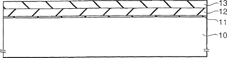
The manufacturing step that following basis is concrete is introduced the manufacture method of semiconductor device of the present invention in proper order.Fig. 3 to 6 shows the profile of the manufacturing step that forms element isolation zone of the present invention.
As shown in Figure 3, silicon oxide film 11 at first is formed on the Semiconductor substrate 10, and silicon nitride film 12 is formed on the silicon oxide film 11.Silicon oxide film 13 is formed on the silicon nitride film 12.
Next, as shown in Figure 4, the photoresist film 14 of composition is formed on the silicon oxide film 13.Use photoresist film 14 optionally to remove silicon oxide film 11 and 13 and silicon nitride film 12 as mask.After this, remove photoresist film 14.
Next, as shown in Figure 5, use silicon oxide film 11 and 13 and silicon nitride film 12 remove part semiconductor substrate 10 corresponding to element isolation zone, formation groove 15 in Semiconductor substrate 10 thus as mask by reactive ion etching (RIE).
Subsequently, as shown in Figure 6, silicon oxide film 16 is formed on the whole surface of resulting structures, uses silicon oxide film 16 filling grooves 15 thus.
Next, as shown in Figure 7, by the smooth silicon oxide film 16 of chemico-mechanical polishing (CMP) method, polishing is up to the surface of exposing silicon nitride film 12.
Afterwards, remove silicon oxide film 11 and 16 and silicon nitride film 12, the surface of exposing Semiconductor substrate 10 thus by wet corrosion.
By this processing, as shown in Figure 8, element isolation zone 17 is formed in the Semiconductor substrate 10, and after this, silicon oxide film 18 is formed on the whole surface of resulting structures.
Fig. 9 to 15 shows the profile that gate electrode forms step.
As shown in Figure 9, at first the photoresist film (not shown) of composition is formed on the Semiconductor substrate 10.Use photoresist film to carry out ion and inject and spread, in the surface of Semiconductor substrate 10, form p type trap 21 as mask.After this, remove photoresist film.With with the same way as of introducing above, on p type trap 21, form the photoresist film (not shown) of composition.Use photoresist film to carry out ion and inject and spread, in the surface of Semiconductor substrate 10, form n type trap 22 as mask.After this, remove photoresist film.Subsequently, in Semiconductor substrate 10, form n channel region 23 and p channel region 24 respectively in the surface of P and N type trap 21 and 22.Remove oxide-film 18 then.Next, on Semiconductor substrate 10, form gate insulating film 25.When forming gate insulating film 25, use pure gas or by oxygen with contain NO, N
2O and NH
3In the mist that makes of any nitrogen carry out the oxide/nitride reaction.Therefore, forming by containing nitrogen concentration is the film formed gate insulating film 25 of about silica of 2% to 10%.Notice that the method that forms gate oxidation films 25 and high concentration region is not limited to above method.For example, with form silicon oxide film as base material then by containing above NO, N
2O and NH
3In the mode of any gas nitriding silicon oxide film form gate insulating film 25.
Subsequently, on gate insulating film 25, form polysilicon film 26.
Next, on polysilicon film 26, form the photoresist film (not shown).After this, as shown in figure 10, use photoresist film optionally to remove polysilicon film 26 and gate insulating film 25 by RIE as mask.Thus, form polygate electrodes 27.
Subsequently, as shown in figure 11, the surface of polygate electrodes 27 and Semiconductor substrate 10 is formed stake shape oxide-film 28 thus by the oxidation of atmosphere column on the whole surface of resulting structures.
Therefore, because oxidized gate electrode 27 has suppressed the oxidation of Semiconductor substrate 10 near surfaces, therefore controlled the growth of stake shape oxide-film 28 on the Semiconductor substrate 10.On the contrary, to the oxidation on the surface of polygate electrodes 27 and diffusion layer 32 surfaces oxidation more than 27 times Semiconductor substrate 10 of gate electrode.
For example, when carrying out oxidation by annealing, Semiconductor substrate 10 oxidized about 6nm when gate oxidation films is nonnitrogenous under 800 ℃ the temperature and under the condition in 30 minutes processing time.On the other hand, in the semiconductor device with the thick gate insulating film that contains about 2% nitrogen of concentration of 3.5nm, Semiconductor substrate 10 is the about 1nm of oxidation only.
Next, as shown in figure 12, on P trap 21, form the photoresist film 29 of composition.Use photoresist film 29 to make mask and introduce impurity, in surface, form P type extension area 30 thus corresponding to the Semiconductor substrate 10 of N trap 22 on the surface of Semiconductor substrate 10.After this, remove photoresist film 29.
Subsequently, as shown in figure 13, on N trap 22, optionally form the photoresist film 31 of composition.Use photoresist film 31 to make mask and introduce impurity, in surface, form N type extension area 32 thus corresponding to the Semiconductor substrate 10 of P trap 21 on the surface of Semiconductor substrate 10.After this, remove photoresist film 31.
On the whole surface of resulting structures shown in Figure 14, form silicon nitride film 33.
Optionally remove silicon nitride film 33 by RIE, on gate electrode sidewall, form grid sidewalls (wall 34).Next, on N trap 22, optionally form the photoresist film (not shown) of composition.Use photoresist film to make mask and introduce impurity, in surface, form N type diffusion region 35 thus corresponding to the Semiconductor substrate 10 of P trap 21 on the surface of Semiconductor substrate 10.After this, remove photoresist film.Next, on P trap 21, optionally form the photoresist film (not shown) of composition.Use photoresist film to make mask and introduce impurity, in surface, form p type diffusion region 36 thus corresponding to the Semiconductor substrate 10 of N trap 22 on the surface of Semiconductor substrate 10.After this, remove photoresist film.
Form CMOS FET in the mode of introducing above, after this carry out the formation that known silicide step and metallization step have been finished LSI afterwards.
Introduce the CONCENTRATION DISTRIBUTION of nitrogen in the semiconductor device of the present invention below with reference to Figure 16 and 17.In the present invention, the surface of the high concentration N district contact semiconductor substrate 10 in the gate insulating film 25.This is owing to there is a spot of nitrogen in the surface of Semiconductor substrate 10, therefore can suppress the oxidation of Semiconductor substrate 10.In addition, silicon nitride demonstrates the high dielectric constant of ratio silicon oxide usually.When the content of nitrogen was too many, it is big that the dielectric constant of gate oxidation films becomes, and through current increases.Experiment shows if the concentration of nitrogen is about 10%, can suppress the through current of MOS transistor so.
In the present embodiment, as shown in figure 16, the high concentration region of nitrogen is formed on the surface near the gate insulating film 25 of Semiconductor substrate 10.As shown in figure 17, to demonstrate nitrogen concentration the highest for the boundary member between the surface of Semiconductor substrate 10 and the gate insulating film 25.
The profile of semiconductor device according to the invention at length is presented among Figure 18.At first, thickness is that the oxide-film 28a of 2.5nm is formed on the part surface of semiconductor device, vertically not overlapping with polygate electrodes 27, thickness is that the following oxide-film 28b of 1nm is formed on the part surface of Semiconductor substrate 10, and is vertically overlapping with polygate electrodes 27.Thickness is the side that the oxide-film 28c of 12nm is formed on polygate electrodes 27, and thickness is the bight that the above oxide-film 28d of 3nm is formed on polygate electrodes 27, and is vertically overlapping with gate insulating film 25.As mentioned above, with reference to the gate insulating film 25 that is formed on gate electrode 27 bights, the thickness of oxide-film 28b is below 1/3rd of oxide-film 28d thickness.When gate oxidation films was nonnitrogenous, the thickness of oxide-film 28b increased.
Figure 19 shows the graph of a relation of the performance of the nitrogen concentration that is contained in the semiconductor device of the present invention in the gate insulating film and MOS transistor.In Figure 19, abscissa shows the nitrogen concentration (%) that is contained in the gate insulating film, and ordinate shows by the grid leakage current of zero expression and the drain current degradation rate of being represented by ■.The drain current degradation rate is set to 1 ratio for leakage current when nitrogen concentration is 0%.
Along with the increase of nitrogen concentration, Leakage Current reduces.Yet leakage current also reduces.Because leakage current is directly proportional with actuating force, so the actuating force of MOS transistor reduces.Though Leakage Current should be little, the nitrogen concentration increase can make MOS transistor not work too much.The limit of supposing drain current degradation is 10% o'clock, and the nitrogen concentration that is contained in the gate oxidation films should be about 2% to 10%.
According to the present invention, shown in Fig. 2 B, though carry out the oxidation of gate electrode 27 sidewalls when forming the column oxide-film, owing in the surface of Semiconductor substrate 10, have nitrogenous high concentration region 40, so can control oxidation to Semiconductor substrate 10.Therefore, the increase of gate electrode 27 bight oxide thickness can be controlled to half that is about prior art.In other words, can control because the leakage of the power line that the thickness increase of gate electrode 27 bight oxide-films causes.Therefore, the reduction of gate electrode can be prevented, and transistorized control ability can be improved.In addition, when the extension diffusion layer of formation source/drain electrode, the protection oxide-film when gate insulating film can be used as ion and injects.Because therefore increase that can the control gate insulator film thickness can prevent to be injected into the minimizing of impurity dose in the Semiconductor substrate.Therefore, compared with prior art, the flying distance of ion shortens.Because can control the ion of injection spreads widely.Thus, can form accurate impurity concentration section.
In the bight of gate electrode 27, because the radius curve in oxidation gate electrode 27 bights becomes big, the electric field that therefore can relax in gate electrode 27 bights is concentrated.The method of noting the oxidation gate electrode is not limited to annealing, also can for example carry out oxidation by RTO (rapid thermal oxidation) to gate electrode under the condition in 50 seconds processing time under 1053 ℃ temperature for example.
As mentioned above, according to the present invention, a kind of semiconductor device and manufacture method thereof are provided, can be controlled at the gate electrode bight and produce Leakage Current, and can reduce formation source/leakages diffusion layer the time ion injection period be injected into the minimizing of the interior impurity dose of Semiconductor substrate.
Be considered to the preferred embodiments of the present invention at present though illustrate and introduced, it should be appreciated by those skilled in the art and to carry out variations and modifications, can substitute device of the present invention with equivalent, and not break away from actual range of the present invention.In addition, can carry out many modifications with suitable specific situation or material according to instruction of the present invention, and not break away from main scope of the present invention.Therefore, the present invention is not limited to as all embodiment in the scope of implementing the disclosed specific embodiment of best mode of the present invention, in fact the present invention includes to fall into the accessory claim book.
Claims (4)
1. semiconductor device comprises:
Semiconductor substrate;
Be formed on the gate insulating film on the described Semiconductor substrate, the nitrogen concentration peak value of described gate insulating film is arranged on the near surface of described Semiconductor substrate;
Be formed on the gate electrode on the described gate insulating film; And
Be formed on the oxide-film on described surface gate electrode and the described Semiconductor substrate,
Wherein said gate insulating film has the first under the core that is positioned at described gate electrode, and be positioned at second portion below the described gate electrode edge, described second portion is thicker than described first, the first surface of described first and second surface define first and second parallel lines that intersect with described second portion, described first parallel lines are between described first and described substrate, described second parallel lines are between described first and described gate electrode, and that a part of thickness between described first parallel lines and described substrate in the described second portion is below 1/3rd of another part thickness between described second parallel lines and described gate electrode in the described second portion.
2. according to the semiconductor device of claim 1, wherein said gate insulating film is to contain the oxide-film that concentration range is 2% to 10% nitrogen.
3. the manufacture method of a semiconductor device may further comprise the steps:
Form gate insulating film on Semiconductor substrate, the nitrogen concentration peak value of described gate insulating film is arranged on the near surface of Semiconductor substrate;
On described gate insulating film, optionally form gate electrode; And
The surface of described gate electrode of oxidation and described Semiconductor substrate, on the surface of described surface gate electrode and described Semiconductor substrate, form oxide-film thus, so that on the gate insulating film in the bight of described gate electrode, the thickness of described Semiconductor substrate one side is below 1/3 of thickness of described gate electrode one side.
4. according to the manufacture method of the semiconductor device of claim 3, the described gate insulating film that wherein is sitting under the described gate electrode contains the oxide-film that concentration range is 2% to 10% nitrogen.
Applications Claiming Priority (2)
| Application Number | Priority Date | Filing Date | Title |
|---|---|---|---|
| JP187970/1999 | 1999-07-01 | ||
| JP11187970A JP2001015748A (en) | 1999-07-01 | 1999-07-01 | Semiconductor device and manufacture thereof |
Publications (2)
| Publication Number | Publication Date |
|---|---|
| CN1284748A CN1284748A (en) | 2001-02-21 |
| CN1264225C true CN1264225C (en) | 2006-07-12 |
Family
ID=16215344
Family Applications (1)
| Application Number | Title | Priority Date | Filing Date |
|---|---|---|---|
| CN00122716.5A Expired - Fee Related CN1264225C (en) | 1999-07-01 | 2000-06-30 | Semiconductor device having nitrogen gate containing insulating film and manufacturing method |
Country Status (4)
| Country | Link |
|---|---|
| US (2) | US6498374B1 (en) |
| JP (1) | JP2001015748A (en) |
| CN (1) | CN1264225C (en) |
| TW (1) | TW535191B (en) |
Families Citing this family (12)
| Publication number | Priority date | Publication date | Assignee | Title |
|---|---|---|---|---|
| JP2001291861A (en) * | 2000-04-05 | 2001-10-19 | Nec Corp | Mos transistor and method for manufacturing the same |
| JP2002026139A (en) | 2000-06-30 | 2002-01-25 | Toshiba Corp | Semiconductor device and manufacturing method therefor |
| JP2002270833A (en) * | 2001-03-14 | 2002-09-20 | Mitsubishi Electric Corp | Semiconductor device and method of manufacturing the same |
| US6921743B2 (en) * | 2001-04-02 | 2005-07-26 | The Procter & Gamble Company | Automatic dishwashing compositions containing a halogen dioxide salt and methods for use with electrochemical cells and/or electrolytic devices |
| KR100464535B1 (en) * | 2002-05-20 | 2005-01-03 | 주식회사 하이닉스반도체 | A method for forming a transistor of a semiconductor device |
| JP2004221246A (en) * | 2003-01-14 | 2004-08-05 | Seiko Epson Corp | Semiconductor device and its manufacturing method |
| JP2005064317A (en) * | 2003-08-18 | 2005-03-10 | Semiconductor Leading Edge Technologies Inc | Semiconductor device |
| US7005333B2 (en) * | 2003-12-30 | 2006-02-28 | Infineon Technologies Ag | Transistor with silicon and carbon layer in the channel region |
| US7002224B2 (en) * | 2004-02-03 | 2006-02-21 | Infineon Technologies Ag | Transistor with doped gate dielectric |
| US7094671B2 (en) * | 2004-03-22 | 2006-08-22 | Infineon Technologies Ag | Transistor with shallow germanium implantation region in channel |
| JP2006253311A (en) * | 2005-03-09 | 2006-09-21 | Toshiba Corp | Semiconductor device and its manufacturing method |
| JP2013125826A (en) * | 2011-12-14 | 2013-06-24 | Renesas Electronics Corp | Semiconductor device and method of manufacturing the same |
Family Cites Families (4)
| Publication number | Priority date | Publication date | Assignee | Title |
|---|---|---|---|---|
| JPH0730113A (en) * | 1993-07-09 | 1995-01-31 | Sony Corp | Manufacture of mos transistor |
| JPH09312393A (en) * | 1996-05-22 | 1997-12-02 | Mitsubishi Electric Corp | Semiconductor device and manufacture thereof |
| JP3312102B2 (en) | 1996-11-27 | 2002-08-05 | シャープ株式会社 | Manufacturing method of nonvolatile semiconductor memory device |
| JP3754234B2 (en) * | 1998-04-28 | 2006-03-08 | インターナショナル・ビジネス・マシーンズ・コーポレーション | Method for forming oxide film on side wall of gate structure |
-
1999
- 1999-07-01 JP JP11187970A patent/JP2001015748A/en active Pending
-
2000
- 2000-06-29 TW TW089112854A patent/TW535191B/en not_active IP Right Cessation
- 2000-06-30 US US09/609,314 patent/US6498374B1/en not_active Expired - Fee Related
- 2000-06-30 CN CN00122716.5A patent/CN1264225C/en not_active Expired - Fee Related
-
2002
- 2002-12-02 US US10/307,405 patent/US20030119235A1/en not_active Abandoned
Also Published As
| Publication number | Publication date |
|---|---|
| US20030119235A1 (en) | 2003-06-26 |
| JP2001015748A (en) | 2001-01-19 |
| US6498374B1 (en) | 2002-12-24 |
| CN1284748A (en) | 2001-02-21 |
| TW535191B (en) | 2003-06-01 |
Similar Documents
| Publication | Publication Date | Title |
|---|---|---|
| CN1215554C (en) | CMOS device and its manufactrue | |
| CN1293637C (en) | CMOS possessing strain channel and preparation method | |
| US7541246B2 (en) | Method of manufacturing semiconductor device | |
| CN1271682C (en) | Method for mfg. semiconductor device with differential thickness grid insulation film | |
| CN1264225C (en) | Semiconductor device having nitrogen gate containing insulating film and manufacturing method | |
| CN1282230C (en) | Method for mfg. semiconductor device, and semiconductor device | |
| CN1505114A (en) | Method for fabricating semiconductor device | |
| CN1841772A (en) | Semiconductor device and method for fabricating the same | |
| CN1195199A (en) | Field effect transistor and method of manufacturing same | |
| CN1619817A (en) | Semiconductor devices having different gate dielectrics and methods for manufacturing the same | |
| CN1663051A (en) | Semiconductor device and its manufacturing method | |
| KR100839359B1 (en) | Method for manufacturing pmos transistor and method for manufacturing cmos transistor | |
| CN1744318A (en) | Semiconductor device and method for fabricating the same | |
| CN1467824A (en) | Semiconductor device and method for manufacturing thereof | |
| CN1571166A (en) | Semiconductor device and method of manufacturing the same | |
| CN1812103A (en) | Semiconductor device having a silicon layer in a gate electrode | |
| CN1421908A (en) | Method for producing MOS transistor with shallow-source electrode/drain electrode junction region | |
| CN1906768A (en) | Semiconductor device and method for manufacturing same | |
| CN1612347A (en) | Semiconductor IC device | |
| CN1542947A (en) | Method of manufacturing semiconductor device | |
| JPH10125906A (en) | Semiconductor device and manufacture thereof | |
| JP3681525B2 (en) | Manufacturing method of semiconductor device | |
| KR100281135B1 (en) | Method for forming gate oxide film of semiconductor device | |
| US7056816B2 (en) | Method for manufacturing semiconductor device | |
| CN1291455C (en) | Method for mfg. semiconductor device |
Legal Events
| Date | Code | Title | Description |
|---|---|---|---|
| C10 | Entry into substantive examination | ||
| SE01 | Entry into force of request for substantive examination | ||
| C06 | Publication | ||
| PB01 | Publication | ||
| C14 | Grant of patent or utility model | ||
| GR01 | Patent grant | ||
| C17 | Cessation of patent right | ||
| CF01 | Termination of patent right due to non-payment of annual fee |
Granted publication date: 20060712 Termination date: 20130630 |