CN1244121C - Electronic source with plane emission area and focusing structure - Google Patents

Electronic source with plane emission area and focusing structure Download PDF

Info

Publication number
CN1244121C
CN1244121C CNB011395001A CN01139500A CN1244121C CN 1244121 C CN1244121 C CN 1244121C CN B011395001 A CNB011395001 A CN B011395001A CN 01139500 A CN01139500 A CN 01139500A CN 1244121 C CN1244121 C CN 1244121C
Authority
CN
China
Prior art keywords
electron source
electrode
insulating barrier
diaphragm
emitter region
Prior art date
Legal status (The legal status is an assumption and is not a legal conclusion. Google has not performed a legal analysis and makes no representation as to the accuracy of the status listed.)
Expired - Lifetime
Application number
CNB011395001A
Other languages
Chinese (zh)
Other versions
CN1372290A (en
Inventor
H·-P·顾
H·比雷基
S·-T·林
S·L·纳伯惠斯
Current Assignee (The listed assignees may be inaccurate. Google has not performed a legal analysis and makes no representation or warranty as to the accuracy of the list.)
Samsung Electronics Co Ltd
Original Assignee
Hewlett Packard Co
Priority date (The priority date is an assumption and is not a legal conclusion. Google has not performed a legal analysis and makes no representation as to the accuracy of the date listed.)
Filing date
Publication date
Application filed by Hewlett Packard Co filed Critical Hewlett Packard Co
Publication of CN1372290A publication Critical patent/CN1372290A/en
Application granted granted Critical
Publication of CN1244121C publication Critical patent/CN1244121C/en
Anticipated expiration legal-status Critical
Expired - Lifetime legal-status Critical Current

Links

Images

Classifications

    • HELECTRICITY
    • H01ELECTRIC ELEMENTS
    • H01JELECTRIC DISCHARGE TUBES OR DISCHARGE LAMPS
    • H01J3/00Details of electron-optical or ion-optical arrangements or of ion traps common to two or more basic types of discharge tubes or lamps
    • H01J3/02Electron guns
    • BPERFORMING OPERATIONS; TRANSPORTING
    • B82NANOTECHNOLOGY
    • B82YSPECIFIC USES OR APPLICATIONS OF NANOSTRUCTURES; MEASUREMENT OR ANALYSIS OF NANOSTRUCTURES; MANUFACTURE OR TREATMENT OF NANOSTRUCTURES
    • B82Y10/00Nanotechnology for information processing, storage or transmission, e.g. quantum computing or single electron logic
    • GPHYSICS
    • G11INFORMATION STORAGE
    • G11BINFORMATION STORAGE BASED ON RELATIVE MOVEMENT BETWEEN RECORD CARRIER AND TRANSDUCER
    • G11B9/00Recording or reproducing using a method not covered by one of the main groups G11B3/00 - G11B7/00; Record carriers therefor
    • G11B9/10Recording or reproducing using a method not covered by one of the main groups G11B3/00 - G11B7/00; Record carriers therefor using electron beam; Record carriers therefor
    • GPHYSICS
    • G11INFORMATION STORAGE
    • G11BINFORMATION STORAGE BASED ON RELATIVE MOVEMENT BETWEEN RECORD CARRIER AND TRANSDUCER
    • G11B9/00Recording or reproducing using a method not covered by one of the main groups G11B3/00 - G11B7/00; Record carriers therefor
    • G11B9/12Recording or reproducing using a method not covered by one of the main groups G11B3/00 - G11B7/00; Record carriers therefor using near-field interactions; Record carriers therefor
    • G11B9/14Recording or reproducing using a method not covered by one of the main groups G11B3/00 - G11B7/00; Record carriers therefor using near-field interactions; Record carriers therefor using microscopic probe means, i.e. recording or reproducing by means directly associated with the tip of a microscopic electrical probe as used in Scanning Tunneling Microscopy [STM] or Atomic Force Microscopy [AFM] for inducing physical or electrical perturbations in a recording medium; Record carriers or media specially adapted for such transducing of information
    • G11B9/1409Heads
    • HELECTRICITY
    • H01ELECTRIC ELEMENTS
    • H01JELECTRIC DISCHARGE TUBES OR DISCHARGE LAMPS
    • H01J2201/00Electrodes common to discharge tubes
    • H01J2201/30Cold cathodes
    • H01J2201/308Semiconductor cathodes, e.g. having PN junction layers

Abstract

A semi-conductor electron source (102) includes a planar emission region (114) for generating an electron emission, and a focusing structure (118, 120) for focusing the electron emission into an electron beam.

Description

Electron source with plane emission area and focusing structure
Technical field
All things considered of the present invention relates to electron source.More specifically, the present invention relates to the electron source of based semiconductor.
Background technology
The electron source of the generation focused beam of based semiconductor can be used for information recording device, lithography application.And other adopts the device of this focused beam.Please consider the example of memory device.In decades, the researcher is constantly making great efforts to improve storage density and reduction information recording device, for example carrying cost of magnetic hard disk drives, CD-ROM driver and semiconductor RAM always.But because routine techniques demonstrates the limit of approaching basic storage density, it is more and more difficult that the raising of storage density is becoming.For example, based on the information stores of conventional magnetic recording rapidly near for example super paramagnetic limit of the basic physics limit, the magnetic potential instability under this limit during room temperature.
The memory device that can not face these basic limit is obtaining research.At United States Patent (USP) 5,557, the example to this information recording device in 596 is described.This device comprises a plurality of electron sources with electron emitting surface, and storage medium is close on this surface.When carrying out write operation, electron source is with the beam bombardment storage medium of high relatively density.During carrying out read operation, electron source is with the beam bombardment storage medium of low relatively density.
Can reduce the size of the bank bit in this device by the diameter that reduces electron beam.The size that reduces bank bit has also just improved storage density and capacity and has reduced carrying cost.
A kind of electron source that adopts in display comprises many " Spindt " reflector.The Spindt reflector can be used to produce focused beam, and this electron beam can be used for data storage device, lithography application and other adopts the application of this focused beam.The Spindt reflector has cone shape, and it is at its cone tip divergent bundle.This circular cone top is processed to sharp as much as possible to reduce operating voltage and to obtain little beam diameter.
But, Spindt reflector existing problems.The reflector top of making point be difficulty and the expense costliness.It is difficult from Spindt reflector top electron beam being focused on stable manner on time and the space.Provide the optical system of this focusing can become complicated.In addition, under the bad condition of vacuum, the Spindt reflector can not be worked well.When beam diameter is reduced to 100 nanometers when following, it is especially remarkable that these problems become.
No matter single transmit device or many reflectors, people expect to reduce manufacturing cost and improve stability and to the operability of electron source.People also expect to reduce beam diameter.
Summary of the invention
According to an aspect of the present invention, electron source comprises a plane emission area; With a focusing structure that is used for the emitter region.According to the present invention, a kind of electron source is provided, comprising: active substrate; One deck on this substrate, this one deck comprise the porous silicon electron-emitting area on plane; The mask of the formation pattern on this laminar surface, the perforate in the mask of this formation pattern defines this emitter region; And the focusing structure that is used for this emitter region.By the following detailed description that the principle of the invention is described by way of example, and make other aspects and advantages of the present invention will become obvious in conjunction with the accompanying drawings.
Description of drawings
Fig. 1 is the schematic diagram according to electron source of the present invention.
Fig. 2 is the flow chart of the manufacture method of electron source shown in Figure 1.
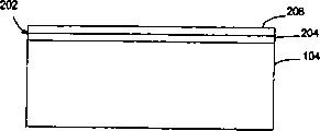
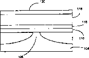
Fig. 3 is the structural representation behind the upper surface deposition mask stacking of substrate.
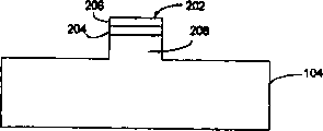
Fig. 4 a forms pattern and the structural representation after exposing mesa structure of being etched at the mask stacking.
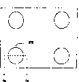
Fig. 4 b is the vertical view of the arranged in patterns of mask stacking.
Fig. 4 c is the vertical view of the another kind of arranged in patterns of mask stacking.
Fig. 5 is the structural representation after the grow oxide district.
Fig. 6 is the structural representation after the leveling.
Fig. 7 is the structural representation after the depositing semiconductor layers on the leveling structure.
Fig. 8 is the structural representation behind deposition emitter on the semiconductor layer.
Fig. 9 is the structural representation after the deposited oxide layer on emitter.
Figure 10 is the structural representation behind deposition lens electrode on the oxide skin(coating).
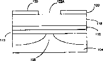
Figure 11 is the structural representation behind etching diaphragm (aperture) on the lens electrode.
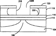
Figure 12 forms tunneling groove structural representation afterwards in oxide skin(coating).
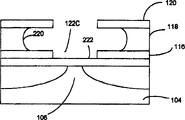
Figure 13 is the structural representation after the etching diaphragm in emitter.
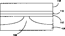
Figure 14 forms porous region structural representation afterwards in the semiconductor layer that exposes to the open air
Figure 15 is according to another kind of electron source schematic diagram of the present invention.
Figure 16 is according to another electron source schematic diagram more of the present invention.
Figure 17 is the schematic diagram according to the another kind of focusing structure of electron source of the present invention.
Figure 18 and 19 is according to other electron source schematic diagram of the present invention.
Embodiment
With reference to Fig. 1, electron source 102 comprises the substrate 104 that can make with silicon.The part of substrate 104 is etched away, stay the next one " activity " district 106.Active region 106 is volcano shape, funnel shaped or nozzle geometry: the bottom is wide and narrow into neck rapidly.
This active region 106 by an isolated area 108 around.108 pairs of active regions 106 of isolated area provide particular geometric shapes.Isolated area 108 also can be kept apart the active region of active region 106 with the neighbour.But the bottom of the active region of contiguous electron source 102 may connect together mutually.
Semiconductor layer 110 is formed on the top at substrate 104.Semiconductor layer 110 can be made by material such as polysilicon or carborundum (SiC).The upper surface of semiconductor layer 110 is plane.
112 districts of semiconductor layer 110 are zones of porous.Porous region 112 aligns with the neck of the active region 106 of volcano shape and terminates in the plane surface of semiconductor layer 110 so that limit an emitter region 114 at plane surface.So emitter region 114 also is plane.Plane permission is made in emitter region 114 to be focused on better to electron beam.By restriction to emitter region 114 areas as described below owing to increased thermal dissipation, so allow higher current density.Can be with the area constraints of emitter region less than 1% of the obtainable emission gross area.
Electron source 102 also is included in emitter 116 on the semiconductor layer 110, at insulating barrier on the emitter 116 118 and the lens electrode on insulating barrier 118 120.Insulating barrier 118 is kept apart emitter 116 and lens electrode 120.Diaphragm 122 extends through lens electrode 120, insulating barrier 118 and emitter 116 and emitter region 114 is exposed.Emitter region 114 is no more than 95% of diaphragm 122 sizes.And diaphragm 122 can adopt wide variety of sizes.
Can cover subregion, the emission electrode 114 of emitter region 114 with conductive layer 124, and lens electrode 120.The 124a of first of conductive layer 124 covers the subregion of emitter region 114 and emitter 116, and the second portion 124b of conductive layer 124 covers lens electrode 120.Because the conductivity of porous silicon region 112 is not strong, so the 124a of first provides connection and permission to whole emitter region 114 to apply electric field on emitter region 114.Can adopt the large-scale gap between 124a of first and the lens electrode 120.
Conductive layer 124 can be to form the oxide of insulation or the alloy of nitride on the surface.Conductive layer 124 can be to be made as gold, carbon (for example graphite or conductive diamond or its combination), platinum, iridium, rhodium, boron nitride or other conductor or semiconductor by thin metal or electric conducting material.The material that atomic number is lower than the atomic number of gold fully also can be used as conductive layer 124.As the element of low atomic number, carbon demonstrates low-down electron scattering probability, and this character can improve electronic transmitting efficiency and reduce the energy spread of emitting electrons.
Conductive layer 124 can be that porous or half densification make all conductive regions for being electrically connected.For example, conductive layer 124 can comprise the conducting island of mutual electrical connection, the net that interconnective filament constitutes, the perhaps combination of the two.
Another side at substrate 104 can form back contact 126.Back contact 126 has been set up an equipotentiality surface for the internal field in Semiconductor substrate 104 and the porous silicon region 112.If substrate 104 is highly doped, can omit back contact 126, substrate 104 connects by front contact in this case.
When operation, on substrate 104, emitter 116, lens electrode 120 and back contact 126, apply different potentials.Consequent emitter voltage causes that electronics is injected into porous region 112 and from the emitter region 114 and be launched through the 124a of first of conductive layer 124 from substrate 104.The electric field that is produced by the electron lens voltage that is positioned at diaphragm 122 places makes this emitting electrons be focused into electron beam 128.Be applied to potential on the lens electrode 120 by change and can adjust focusing electron beam 128.Electron beam 128 can be focused into very little point (for example, diameter is less than a nanometer) on target 12 (for example, storage medium).
The driving power that applies potential on substrate 104 and electrode 116 and 102 can be on chip (off-chip) (on-chip) and that leave chip.
Fig. 2 has summed up a kind of possible method of making electron source 102.Make at substrate 104 surperficial tops formation mask stackings (step 162) by deposit the chromium layer in substrate 104 surface deposition one deck pad oxide layer and on this pad oxide layer.
Carry out etching formation active region 106 (step 164) with this chromium layer patternization and to this substrate.The growth insulating barrier is so that isolate (step 166) and consequent structure is carried out complanation (step 168) active region 106.
In planarization surface depositing semiconductor layers (170).So it is plane that semiconductor layer also is.
Form emission electrode 116 (step 172) at semiconductor layer 110 tops.For example, can form emission electrode 116 on the semiconductor 110 by chromium (Cr) is deposited upon.
Insulating barrier 118 (step 174) is formed on the top at emission electrode 116.Insulating barrier 118 can be an oxide skin(coating).
Lens electrode 120 (step 176) is formed on the top at insulating barrier 118.For example, can form lens electrode 120 by on insulating barrier 118, depositing chromium (Cr) layer.
In lens electrode 120, insulating barrier 118 and emission electrode 116, form diaphragm 122 (step 178).Can insulating barrier 118 is recessed to avoid interference electron beam.Diaphragm 122 extends to semiconductor layer 110.So diaphragm exposes emitter region 114.
Can pass through certain technology, for example anode oxidation process is made 112 districts of semiconductor layer 110 (step 180) of porous.On emitter region 114 and electrode 116 and 120, formed conductive layer 124 (step 182) so.
Can be to porous region 12 patternings to form a plurality of independently emitter regions.At run duration, can simultaneously or carry out addressing to these emitter regions selectively.
Fig. 3 to Figure 14 shows the electron source 102 in each stage of the manufacturing process of example.Fig. 3 has showed silicon substrate 104 and has formed mask stacking 202 at substrate 104 surperficial tops.Substrate 104 can be that its electrical resistivity range of silicon substrate of n++ type is less than 0.01 ohm-cm.Mask stacking 202 can comprise pad oxide layer 204 and mask material layer 206.Can form pad oxide layer 204 by adopting wet method or dry oxidation technology grown silicon oxide skin(coating) on substrate surface.
With reference to Fig. 4 a, can adopt conventional photoetching technique to mask stacking 202 patternings, and the size and the position that can be limited according to the mask stacking 202 of patterning etch the active device regions 208 with mesa shape on substrate 104.Can adopt dry etching technology to form active device regions 208.Active region 208 can be the cylindrical shape shown in Fig. 4 b.The diameter of such active region 208 can be several microns or preferably one to two micron.
Active region 208 is not limited to cylindrical shape.For example, this active region can have the circle of the hollow shown in Fig. 4 c.Fig. 4 b and Fig. 4 c also show a plurality of electron sources (each electron source can be addressed separately) that can make simultaneously on single substrate.
With reference to Fig. 5, can be by substrate 104 being exposed to the heat growth of carrying out silicon dioxide isolated area 108 in wet oxidation (for example, water vapour) or the dry oxidation (for example, oxygen).When the growth of finishing oxide, the isolated area 108 of generation is filled into the part that is etched away of substrate 104.As the various results that influence the factor of oxide growth rate, substrate is not etched away by the part that mask covers, and causes surface 210 and sidewall 212 to become circle to a certain extent.
With reference to Fig. 6, after isolated area 108 growths are finished, isolated area 108 and active region 106 are carried out complanation in addition.Can adopt CMP (Chemical Mechanical Polishing) process (CMP) to remove the some parts 214 of active region 106 and isolated area 108.CMP technology produces a basic even curface 216.At this operation stage, active region 106 has the geometry of volcano shape.So active device regions has wide bottom and the formation neck that narrows down rapidly at plane surface 216 places.
With reference to Fig. 7, at structural top employing chemical vapor deposition (CVD) the technology formation polysilicon layer 110 of leveling.The thickness of polysilicon layer 110 can be about 0.01 to 2 micron.
With reference to Fig. 8, by deposition, for example, thickness range is about 0.1 to 1 micron chromium layer, can form emission electrode 116 on semiconductor layer 110.
With reference to Fig. 9, by for example, CVD TEOS (tetraethoxysilane) oxidate forms Si oxide (SiOx) insulating barrier 118 on emission electrode 116.On deposition, after the insulating barrier 118, can insulating barrier 118 be carried out leveling to about 0.01 to 2 micron thickness by CMP.
With reference to Figure 10, by deposition, for example, thickness range is about 0.01 to 1 micron, and 0.1 micron chromium layer preferably, forms lens electrode 120 on insulating barrier 118.
With reference to Figure 11 to Figure 13, run through lens electrode 120, insulating barrier 118 and emission electrode 116 forms diaphragms 122 by etching, at first can be on lens electrode 120 patterning and its etching formed the first diaphragm 122A (Figure 11).Dry etch process such as ion beam milling can be used for etching lens electrode 120.The diameter of the first diaphragm 122A can be several microns and preferably 2 microns.
Can adopt two step etching technics in insulating barrier 118 (Figure 12), to form the second diaphragm 122B.Two step etching technics can comprise dry etch step and the wet etching step of closelying follow.For example, in dry etch step, pass through to adopt CHF 3The RIE etching of etching agent forms that this sidewall of sidewall 218 (shown in broken lines) aligns with the first diaphragm 122A and is vertical with emission electrode 118 basically.Oppose side wall 218 adopts wet-etching technologies to carry out etching and with insulating barrier 118 transverse recess.The result forms the sidewall 220 of the undermining of insulating barrier 118.Can adopt buffer oxide etching agent to carry out wet etching based on hydrofluoric acid.
Then emission electrode 116 being carried out etching forms the 3rd diaphragm 122C and thereby has exposed 222 districts (Figure 13) of semiconductor layer 110.The diameter of the 3rd diaphragm 122C can be greatly aligns with the first diaphragm 122A basically to several microns and it.Can adopt dry etch process that emission electrode 116 is carried out etching.Can carry out slightly etching to the exposed region 222 of semiconductor layer 110 to guarantee exposing semiconductor layer 110 fully.
Figure 12 and step shown in Figure 13 can be put upside down, and form diaphragm 122C thus before undermining wall 220.
Referring now to Figure 14, in semiconductor layer 110, form porous region 112.Can adopt anode processing technique in semiconductor layer 110, to generate porous, this technology is at Xia Sheng, HidekiKoyama, " based on the active surface emission of the cold cathode of electro-luminescent porous silica diode " with Nobuyoshi Koshida, vacuum technology magazine B rolled up for 15 (2) phases, 1998,3/4 month, 793 pages to 795 pages (" Efficient surfaee-emitting cold cathodes based onelectro luminescent porous silicon diode ", J.Vaccum Science TechnologyB15 (2)) be described in the literary composition.By Control current density and anodizing time, can control the porosity rate in the porous region 112.
Form after the porous region 112, can increase conductive layer 124.Conductive layer 124 can similarly cover emitter region 114 and emission electrode 116 and lens electrode 120.The thickness of the conductive layer that employing carbon is made can be about 10 nanometers.Consistent with Fig. 1, the 124a of first of conductive layer 124 covers the part of emitter region 114 and emission electrode 116, and the second portion 124b of conductive layer 124 covers lens electrode 120.
Figure 15 has showed second kind of (another kind) electron source 302.Second kind of electron source 302 also comprises substrate 104, active region 106, insulation layer 108, semiconductor layer 110, porous region 112, emitter region 114 and emission electrode 116.Second kind of electron source 302 also comprise first insulating barrier 118, first lens electrode 120, at second insulating barrier 304 on first lens electrode 120 and second lens electrode 306 on second insulating barrier 304.
Perforate 308 comes out emitter region 114.First and second insulating barriers 118 and 304 are recessedly come in contact with the electron beam of avoiding Yu launch from electron source 302 309.Can emitter region 114 and electroplax 116,120 and 306 be covered with conductive coating.For structure shown in Figure 15, the third part 310c that the second portion 310b that the 310a of first of conductive coating has covered a part, the conductive coating of emitter region 114 and emission electrode 116 has covered first lens electrode 120 and conductive coating has covered second lens electrode 306.
Can advantageously control or focus on by electrode 120 and 306 being applied different operating potential gesture electron beam 309.
So compare with the Spindt reflector, it is easier and more cheap that disclosed electron source 102 and 302 manufactures.Electron source 102 and 302 can focus on the stationary mode on time and space, and they can move under the bad condition of vacuum.This thin conductive layer can also reduce scattering and reduce energy spread thus and improved efficient.
The substrate of this electron source is not limited to silicon.Also can adopt other semi-conducting material.Even can adopt metal material, on metal substrate, form semiconductor layer thus.
The overall dimension of this electron source is decided according to concrete device.To the voltage that electrode applied also is to decide according to concrete device.
The manufacturing of this electron source is not limited to the described step of Fig. 3 to 14.Can adopt that other technology deposits, leveling or the like.Electrode, electric conductor, insulator etc. also can adopt other material.
The emitter region can be adopted except forming the wide active region, bottom and the formation neck that narrows down, and other method that forms at the neck place outside the method for porous region is come patterning.Yet this patterning method provides some advantage.Wide bottom heat dissipation is to carry out heat management preferably.
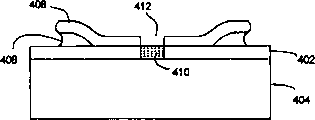
Figure 16 has showed another kind of pattern.Formed polysilicon layer 402 at the top of active n++ substrate 404, insulating barrier 406 is grown on the substrate 404, and the mask 408 of patterning forms at the surperficial top of polysilicon layer 402 and insulating barrier 406.Porous region 410 is positioned at polysilicon layer 412, and the diaphragm in the mask 408 of patterning defines emitter region 412 and the emission electrode (not shown) covers formation patterned mask 408.The mask 408 of patterning can be made by metal or dielectric material.
This focusing structure is not limited to the stacking electrode of being kept apart by insulating barrier.For example, Figure 17 has showed that a kind of focusing structure 502 comprises emission electrode 506 and the lens electrode 508 on the polysilicon layer 504.Lens electrode 508 is around emission electrode 506, and the diaphragm in the emission electrode 506 comes out emitter region 510.
Electron source does not limit to and above-mentioned electron emission structure.Can obtain emitting electrons from plane surface by many technology.This electron source can comprise by the area of heating surface launches thermionic emitting structural.Another kind method can or be lower than under the room temperature condition in room temperature, and electronics comes out from the surface emitting of metal-insulator-metal type (MIM) and metal-insulator-oxide (MIS) structure.This electronics emission type is described in following document: Wande﹠amp; J Briggs " the low noise line of tunnel cathode ", 33 3 phases of volume of applicating physical magazine, 836 pages to 840 pages, (" Low noise Beams from TunnelCathodes ", Journal of Applied Physics 33, No3 in 1962, pp836-840,1962); Julius Cohen " to the tunnel emission of vacuum ", Applied Physics wall bulletin 1 volume, 3 phases, 61 pages-62 pages, (" Tunnel Emission into Vacuum in 1962 " Applied PhysicsLetters1, No3, pp61-62,1962); With " emission characteristicss of Metal-oxide-semicondutor electron tunnel negative electrode " such as Yokoo, the vacuum technology magazine, 429 pages to 432 pages, 1993 (" Emission characteristics of metal-oxide-semiconductor electrontunneling cathode ", Journal of Vacuum Science and Technology, pp.429-432,1993).Electronics is transmitted into the vacuum with small divergence angle from MIM and MIS structure, and as at R.Hrach, 15 pages of thin solid film 15 volumes are described in the document in 1973 (Thin Solid Film15, p.15,1973).The little angle of divergence allows electrons emitted to be focused into the electron beam of minor diameter.
The electron source 602 that Figure 18 shows comprises the electron emission structure based on metal-insulator-metal type (MIM).Between insulator 610 and active region 606, be thin metal layer 612.So this metal-insulator-metal type is corresponding to electrode 124a, insulator 610 and thin metal layer 612.
The electron source 702 that Figure 19 shows comprises the electron emission structure based on metal-insulator semiconductor (MIS).This active region extends to insulator 710.So this metal-insulator semiconductor is corresponding to electrode 124a, insulator 710 and active region 706.
Above-mentioned paragraph is described the structure and the manufacturing of single electron source.But.It will be appreciated that and on single chip, can make a plurality of electron sources simultaneously and on single wafer, can make a plurality of chips simultaneously.
Electron source 102 and 302 can have a lot of application.Application example comprises data information memory device, the electron beam instruments of inspection (for example scanning electron microscopy), and photoetching and imaging show.These electron sources can produce extra small bank bit, produce ultra-fine photoetching line, produce extra small pixel in cathode ray tube or raster display in information recording device.
Although specific embodiment of the present invention is described and shows, the present invention is not limited to the form and the arrangements of described and the parts showed.But the present invention makes an explanation according to following claim.

Claims (8)

1. an electron source (102) comprising:
Active substrate (104);
One deck on this substrate, this one deck comprise the porous silicon electron-emitting area (114) on plane;
The mask of the formation pattern on this laminar surface, the perforate in the mask of this formation pattern defines this emitter region; And
The focusing structure (118,120) that is used for this emitter region.
2. the electron source of claim 1, substrate wherein (104) has the active region (106) of aliging with porous region (114).
3. the electron source of claim 1, focusing structure wherein (118,120) comprises diaphragm (122), electron beam is focused by this diaphragm; And wherein this emitter region (114) have littler size than the diaphragm (122) of focusing structure.
4. the electron source of claim 3, wherein emitter region (114) be not more than focusing structure diaphragm (122) size 95%.
5. the electron source of claim 1 also is included in the conductive layer (124) on the emitter region (114).
6. the electron source of claim 1, emitter region wherein (114) are limited to than 1% of the gross area that can be used for launching also little area.
7. the electron source of claim 1, focusing structure wherein comprises first electrode (116) on the semiconductor layer, the insulating barrier (118) on first electrode (116), and second electrode (120) on the insulating barrier (118); Extend through the diaphragm (122) of electrode (116,120) and insulating barrier (120), this diaphragm exposes emitter region (114).
8. the electron source of claim 7, focusing structure wherein also is included in second insulating barrier (304) on second electrode (120) and the third electrode (306) on second insulating barrier (304), and perforate (308) extends through second insulating barrier (304) and third electrode (306) equally.
CNB011395001A 2001-02-27 2001-11-27 Electronic source with plane emission area and focusing structure Expired - Lifetime CN1244121C (en)

Applications Claiming Priority (2)

Application Number Priority Date Filing Date Title
US09/795240 2001-02-27
US09/795,240 US6815875B2 (en) 2001-02-27 2001-02-27 Electron source having planar emission region and focusing structure

Publications (2)

Publication Number Publication Date
CN1372290A CN1372290A (en) 2002-10-02
CN1244121C true CN1244121C (en) 2006-03-01

Family

ID=25165082

Family Applications (1)

Application Number Title Priority Date Filing Date
CNB011395001A Expired - Lifetime CN1244121C (en) 2001-02-27 2001-11-27 Electronic source with plane emission area and focusing structure

Country Status (5)

Country Link
US (2) US6815875B2 (en)
EP (1) EP1237174A1 (en)
JP (1) JP2002260546A (en)
CN (1) CN1244121C (en)
HK (1) HK1048014A1 (en)

Families Citing this family (18)

* Cited by examiner, † Cited by third party
Publication number Priority date Publication date Assignee Title
US6649431B2 (en) * 2001-02-27 2003-11-18 Ut. Battelle, Llc Carbon tips with expanded bases grown with simultaneous application of carbon source and etchant gases
US6781146B2 (en) * 2001-04-30 2004-08-24 Hewlett-Packard Development Company, L.P. Annealed tunneling emitter
JP4830217B2 (en) * 2001-06-18 2011-12-07 日本電気株式会社 Field emission cold cathode and manufacturing method thereof
DE10225266A1 (en) * 2001-12-19 2003-07-03 Zeiss Carl Smt Ag Imaging device in a projection exposure system
JP2004111292A (en) * 2002-09-20 2004-04-08 Hitachi Displays Ltd Display device and its manufacturing method
JP4298399B2 (en) * 2003-06-26 2009-07-15 キヤノン株式会社 Electron beam apparatus and electron beam drawing apparatus using the electron beam apparatus
US7456491B2 (en) * 2004-07-23 2008-11-25 Pilla Subrahmanyam V S Large area electron emission system for application in mask-based lithography, maskless lithography II and microscopy
WO2006066111A2 (en) * 2004-12-16 2006-06-22 Telegen Corporation Light emitting device and associates methods of manufacture
KR20060095318A (en) * 2005-02-28 2006-08-31 삼성에스디아이 주식회사 Electron emission device and method for manufacturing the same
KR100889527B1 (en) * 2007-11-21 2009-03-19 삼성에스디아이 주식회사 Light emission device and display device using the light emission device as light source
US8084929B2 (en) * 2009-04-29 2011-12-27 Atti International Services Company, Inc. Multiple device shaping uniform distribution of current density in electro-static focusing systems
US8436332B2 (en) 2009-12-17 2013-05-07 Pioneer Corporation Electron emission element and imaging device having the same
WO2011083512A1 (en) * 2010-01-07 2011-07-14 パイオニア株式会社 Electron-emitting element and image pickup device provided with same
NL2007604C2 (en) * 2011-10-14 2013-05-01 Mapper Lithography Ip Bv Charged particle system comprising a manipulator device for manipulation of one or more charged particle beams.
NL2006868C2 (en) 2011-05-30 2012-12-03 Mapper Lithography Ip Bv Charged particle multi-beamlet apparatus.
US9116290B1 (en) * 2011-10-07 2015-08-25 Bae Systems Information And Electronic Systems Integration Inc. Faceted, germanium slotted waveguide
JP6834817B2 (en) * 2016-08-08 2021-02-24 株式会社ニューフレアテクノロジー Aperture for multi-beam inspection, beam inspection device for multi-beam, and multi-charged particle beam drawing device
CN107331619A (en) * 2017-06-28 2017-11-07 京东方科技集团股份有限公司 Thin film transistor (TFT) and preparation method thereof, display device, exposure device

Family Cites Families (19)

* Cited by examiner, † Cited by third party
Publication number Priority date Publication date Assignee Title
US4500791A (en) 1980-06-07 1985-02-19 Dr. -Ing. Rudolf Hell Gmbh High stability electron beam generator for processing material
US4904895A (en) * 1987-05-06 1990-02-27 Canon Kabushiki Kaisha Electron emission device
FR2641412B1 (en) * 1988-12-30 1991-02-15 Thomson Tubes Electroniques FIELD EMISSION TYPE ELECTRON SOURCE
JPH0512988A (en) * 1990-10-13 1993-01-22 Canon Inc Semiconductor electron emitting element
EP0545621B1 (en) * 1991-11-29 1995-09-06 Motorola, Inc. Method of forming a field emission device with integrally formed electrostatic lens
JP3243471B2 (en) 1994-09-16 2002-01-07 三菱電機株式会社 Method for manufacturing electron-emitting device
US5557596A (en) 1995-03-20 1996-09-17 Gibson; Gary Ultra-high density storage device
KR100266517B1 (en) * 1995-07-07 2000-09-15 가네꼬 히사시 Electron-gun provided with a field emission cold cathode and improved gate structure
JP2765533B2 (en) 1995-10-31 1998-06-18 日本電気株式会社 Straight beam microwave tube
JP3512933B2 (en) * 1996-01-25 2004-03-31 株式会社東芝 Field emission cold cathode device and method of manufacturing the same
TW391022B (en) 1997-10-29 2000-05-21 Mitsubishi Rayon Co Field emission electron source, method of producing the same, and use of the same
US6326725B1 (en) * 1998-05-26 2001-12-04 Micron Technology, Inc. Focusing electrode for field emission displays and method
US6190223B1 (en) * 1998-07-02 2001-02-20 Micron Technology, Inc. Method of manufacture of composite self-aligned extraction grid and in-plane focusing ring
TW436837B (en) * 1998-11-16 2001-05-28 Matsushita Electric Works Ltd Field emission-type electron source and manufacturing method thereof and display using the electron source
JP2000268706A (en) 1999-03-18 2000-09-29 Matsushita Electric Ind Co Ltd Electron emitting element and image drawing device using the same
JP2000294122A (en) * 1999-04-08 2000-10-20 Nec Corp Manufacture of field emission cold cathode and flat- panel display
US6498426B1 (en) * 1999-04-23 2002-12-24 Matsushita Electric Works, Ltd. Field emission-type electron source and manufacturing method thereof
US6538367B1 (en) 1999-07-15 2003-03-25 Agere Systems Inc. Field emitting device comprising field-concentrating nanoconductor assembly and method for making the same
JP3487229B2 (en) 1999-07-27 2004-01-13 松下電工株式会社 Field emission type electron source and method of manufacturing the same

Also Published As

Publication number Publication date
JP2002260546A (en) 2002-09-13
EP1237174A1 (en) 2002-09-04
HK1048014A1 (en) 2003-03-14
US20050001530A1 (en) 2005-01-06
US7208867B2 (en) 2007-04-24
US6815875B2 (en) 2004-11-09
US20020117953A1 (en) 2002-08-29
CN1372290A (en) 2002-10-02

Similar Documents

Publication Publication Date Title
CN1244121C (en) Electronic source with plane emission area and focusing structure
CN100385543C (en) Planer electron emitting device unit with improved emitting area and its making process
US6806630B2 (en) Electron emitter device for data storage applications and method of manufacture
US7521851B2 (en) Electron emitting composite based on regulated nano-structures and a cold electron source using the composite
JP2008166257A (en) Carbon nanotube field emission emitter, and its manufacturing method
TW575874B (en) Data storage device
CN1700397A (en) Electron emission device and electron emission display using the same
CN1539152A (en) Tunneling emitter
JP2003162956A (en) Mis/mim electron emitter
JP2005515584A (en) Silicon-based dielectric tunnel emitter
JP2002520770A (en) Field emission element
JP3638264B2 (en) Cold cathode device manufacturing method, cold cathode device, and display device using the same
JPH08306302A (en) Field emission type electron source and its manufacture
TWI281685B (en) Emitter with filled zeolite emission layer
JP2694889B2 (en) Method of forming self-aligned gate structure and focusing ring
JP2001057145A (en) Cold-cathode light source and thin image forming device
JP3097523B2 (en) Method for manufacturing field emission element
JP4093997B2 (en) Anodizing method for improving electron emission in electronic devices
Lee A knife-edge array field emission cathode
JP2001035356A (en) Field emission type electron source and manufacture thereof, and display device
JPH06164034A (en) Solid-state laser

Legal Events

Date Code Title Description
C06 Publication
PB01 Publication
C10 Entry into substantive examination
SE01 Entry into force of request for substantive examination
C14 Grant of patent or utility model
GR01 Patent grant
REG Reference to a national code

Ref country code: HK

Ref legal event code: WD

Ref document number: 1048014

Country of ref document: HK

ASS Succession or assignment of patent right

Owner name: SAMSUNG ELECTRONICS CO., LTD.

Free format text: FORMER OWNER: HEWLETT-PACKARD CO. (US) P.O. BOX 10301, PALO ALTO CALIFORNIA U.S.A.

Effective date: 20110222

C41 Transfer of patent application or patent right or utility model
COR Change of bibliographic data

Free format text: CORRECT: ADDRESS; FROM: STATE OF CALIFORNIA, THE USA TO: GYEONGGI-DO, SOUTH KOREA

TR01 Transfer of patent right

Effective date of registration: 20110222

Address after: Gyeonggi Do, South Korea

Patentee after: Samsung Electronics Co.,Ltd.

Address before: California, USA

Patentee before: Hewlett-Packard Co.

CX01 Expiry of patent term

Granted publication date: 20060301

CX01 Expiry of patent term