CN1539152A - Tunneling emitter - Google Patents
Tunneling emitter Download PDFInfo
- Publication number
- CN1539152A CN1539152A CNA028133072A CN02813307A CN1539152A CN 1539152 A CN1539152 A CN 1539152A CN A028133072 A CNA028133072 A CN A028133072A CN 02813307 A CN02813307 A CN 02813307A CN 1539152 A CN1539152 A CN 1539152A
- Authority
- CN
- China
- Prior art keywords
- layer
- reflector
- electron source
- tunnel
- emission
- Prior art date
- Legal status (The legal status is an assumption and is not a legal conclusion. Google has not performed a legal analysis and makes no representation as to the accuracy of the status listed.)
- Pending
Links
- 230000005641 tunneling Effects 0.000 title claims abstract description 23
- 238000000034 method Methods 0.000 claims abstract description 32
- 230000008569 process Effects 0.000 claims abstract description 17
- 238000000137 annealing Methods 0.000 claims abstract description 11
- 239000000758 substrate Substances 0.000 claims description 31
- 230000004888 barrier function Effects 0.000 claims description 18
- 238000010276 construction Methods 0.000 claims description 15
- 229910052751 metal Inorganic materials 0.000 claims description 14
- 239000002184 metal Substances 0.000 claims description 14
- 229910004465 TaAlO Inorganic materials 0.000 claims description 8
- 239000011248 coating agent Substances 0.000 claims description 6
- 238000000576 coating method Methods 0.000 claims description 6
- 230000000694 effects Effects 0.000 claims description 6
- 229910008807 WSiN Inorganic materials 0.000 claims description 4
- 238000003860 storage Methods 0.000 claims description 3
- 230000004044 response Effects 0.000 claims 4
- 230000015572 biosynthetic process Effects 0.000 claims 1
- 239000012212 insulator Substances 0.000 abstract 1
- 239000010410 layer Substances 0.000 description 106
- 238000005516 engineering process Methods 0.000 description 15
- 230000007797 corrosion Effects 0.000 description 11
- 238000005260 corrosion Methods 0.000 description 11
- 239000000463 material Substances 0.000 description 10
- 239000012790 adhesive layer Substances 0.000 description 9
- 230000005684 electric field Effects 0.000 description 9
- BASFCYQUMIYNBI-UHFFFAOYSA-N platinum Chemical compound [Pt] BASFCYQUMIYNBI-UHFFFAOYSA-N 0.000 description 8
- QVGXLLKOCUKJST-UHFFFAOYSA-N atomic oxygen Chemical compound [O] QVGXLLKOCUKJST-UHFFFAOYSA-N 0.000 description 6
- 239000001301 oxygen Substances 0.000 description 6
- 229910052760 oxygen Inorganic materials 0.000 description 6
- 238000000151 deposition Methods 0.000 description 5
- 230000008021 deposition Effects 0.000 description 5
- PCHJSUWPFVWCPO-UHFFFAOYSA-N gold Chemical compound [Au] PCHJSUWPFVWCPO-UHFFFAOYSA-N 0.000 description 5
- 229910052737 gold Inorganic materials 0.000 description 5
- 239000010931 gold Substances 0.000 description 5
- 239000004065 semiconductor Substances 0.000 description 5
- 239000010409 thin film Substances 0.000 description 5
- OGIDPMRJRNCKJF-UHFFFAOYSA-N titanium oxide Inorganic materials [Ti]=O OGIDPMRJRNCKJF-UHFFFAOYSA-N 0.000 description 5
- 239000010408 film Substances 0.000 description 4
- 238000001020 plasma etching Methods 0.000 description 4
- 229910052697 platinum Inorganic materials 0.000 description 4
- 229910052715 tantalum Inorganic materials 0.000 description 4
- GUVRBAGPIYLISA-UHFFFAOYSA-N tantalum atom Chemical compound [Ta] GUVRBAGPIYLISA-UHFFFAOYSA-N 0.000 description 4
- 229910052723 transition metal Inorganic materials 0.000 description 4
- 150000003624 transition metals Chemical class 0.000 description 4
- VYZAMTAEIAYCRO-UHFFFAOYSA-N Chromium Chemical compound [Cr] VYZAMTAEIAYCRO-UHFFFAOYSA-N 0.000 description 3
- ZOKXTWBITQBERF-UHFFFAOYSA-N Molybdenum Chemical compound [Mo] ZOKXTWBITQBERF-UHFFFAOYSA-N 0.000 description 3
- MWUXSHHQAYIFBG-UHFFFAOYSA-N Nitric oxide Chemical compound O=[N] MWUXSHHQAYIFBG-UHFFFAOYSA-N 0.000 description 3
- OAICVXFJPJFONN-UHFFFAOYSA-N Phosphorus Chemical compound [P] OAICVXFJPJFONN-UHFFFAOYSA-N 0.000 description 3
- KJTLSVCANCCWHF-UHFFFAOYSA-N Ruthenium Chemical compound [Ru] KJTLSVCANCCWHF-UHFFFAOYSA-N 0.000 description 3
- XUIMIQQOPSSXEZ-UHFFFAOYSA-N Silicon Chemical compound [Si] XUIMIQQOPSSXEZ-UHFFFAOYSA-N 0.000 description 3
- 239000000956 alloy Substances 0.000 description 3
- 229910045601 alloy Inorganic materials 0.000 description 3
- 229910052804 chromium Inorganic materials 0.000 description 3
- 239000011651 chromium Substances 0.000 description 3
- 239000004020 conductor Substances 0.000 description 3
- 238000010586 diagram Methods 0.000 description 3
- 229910052741 iridium Inorganic materials 0.000 description 3
- GKOZUEZYRPOHIO-UHFFFAOYSA-N iridium atom Chemical compound [Ir] GKOZUEZYRPOHIO-UHFFFAOYSA-N 0.000 description 3
- 229910052750 molybdenum Inorganic materials 0.000 description 3
- 239000011733 molybdenum Substances 0.000 description 3
- 230000003287 optical effect Effects 0.000 description 3
- 239000003870 refractory metal Substances 0.000 description 3
- 229910052707 ruthenium Inorganic materials 0.000 description 3
- 229910052710 silicon Inorganic materials 0.000 description 3
- 239000010703 silicon Substances 0.000 description 3
- IJGRMHOSHXDMSA-UHFFFAOYSA-N Atomic nitrogen Chemical compound N#N IJGRMHOSHXDMSA-UHFFFAOYSA-N 0.000 description 2
- CURLTUGMZLYLDI-UHFFFAOYSA-N Carbon dioxide Chemical compound O=C=O CURLTUGMZLYLDI-UHFFFAOYSA-N 0.000 description 2
- 229910052782 aluminium Inorganic materials 0.000 description 2
- XAGFODPZIPBFFR-UHFFFAOYSA-N aluminium Chemical compound [Al] XAGFODPZIPBFFR-UHFFFAOYSA-N 0.000 description 2
- 230000008901 benefit Effects 0.000 description 2
- 238000009826 distribution Methods 0.000 description 2
- 239000003344 environmental pollutant Substances 0.000 description 2
- 239000007789 gas Substances 0.000 description 2
- 239000012782 phase change material Substances 0.000 description 2
- 231100000719 pollutant Toxicity 0.000 description 2
- 210000003456 pulmonary alveoli Anatomy 0.000 description 2
- 238000004544 sputter deposition Methods 0.000 description 2
- 238000007740 vapor deposition Methods 0.000 description 2
- UGFAIRIUMAVXCW-UHFFFAOYSA-N Carbon monoxide Chemical compound [O+]#[C-] UGFAIRIUMAVXCW-UHFFFAOYSA-N 0.000 description 1
- JXXICDWXXTZTHN-UHFFFAOYSA-M N.[O-2].[O-2].[OH-].O.[Ta+5] Chemical compound N.[O-2].[O-2].[OH-].O.[Ta+5] JXXICDWXXTZTHN-UHFFFAOYSA-M 0.000 description 1
- GWEVSGVZZGPLCZ-UHFFFAOYSA-N Titan oxide Chemical compound O=[Ti]=O GWEVSGVZZGPLCZ-UHFFFAOYSA-N 0.000 description 1
- CCNUTEKZWXBWKR-UHFFFAOYSA-N [Si].[W].[N+](=O)(O)[O-] Chemical compound [Si].[W].[N+](=O)(O)[O-] CCNUTEKZWXBWKR-UHFFFAOYSA-N 0.000 description 1
- 238000002679 ablation Methods 0.000 description 1
- 239000004411 aluminium Substances 0.000 description 1
- VQLOCUKZAJRPAO-UHFFFAOYSA-N aluminum oxygen(2-) tantalum(5+) Chemical compound [O--].[O--].[O--].[O--].[Al+3].[Ta+5] VQLOCUKZAJRPAO-UHFFFAOYSA-N 0.000 description 1
- 238000013459 approach Methods 0.000 description 1
- 229910002092 carbon dioxide Inorganic materials 0.000 description 1
- 239000001569 carbon dioxide Substances 0.000 description 1
- 229910002091 carbon monoxide Inorganic materials 0.000 description 1
- 230000015556 catabolic process Effects 0.000 description 1
- 230000008859 change Effects 0.000 description 1
- 239000003795 chemical substances by application Substances 0.000 description 1
- 238000005229 chemical vapour deposition Methods 0.000 description 1
- 238000001816 cooling Methods 0.000 description 1
- 238000001312 dry etching Methods 0.000 description 1
- 230000003628 erosive effect Effects 0.000 description 1
- 238000005530 etching Methods 0.000 description 1
- 238000001704 evaporation Methods 0.000 description 1
- 230000008020 evaporation Effects 0.000 description 1
- 239000002784 hot electron Substances 0.000 description 1
- MRNHPUHPBOKKQT-UHFFFAOYSA-N indium;tin;hydrate Chemical compound O.[In].[Sn] MRNHPUHPBOKKQT-UHFFFAOYSA-N 0.000 description 1
- 238000010884 ion-beam technique Methods 0.000 description 1
- 238000002955 isolation Methods 0.000 description 1
- 238000004519 manufacturing process Methods 0.000 description 1
- 239000012528 membrane Substances 0.000 description 1
- 239000000203 mixture Substances 0.000 description 1
- 238000001451 molecular beam epitaxy Methods 0.000 description 1
- 150000004767 nitrides Chemical class 0.000 description 1
- 229910052757 nitrogen Inorganic materials 0.000 description 1
- 239000011368 organic material Substances 0.000 description 1
- BPUBBGLMJRNUCC-UHFFFAOYSA-N oxygen(2-);tantalum(5+) Chemical compound [O-2].[O-2].[O-2].[O-2].[O-2].[Ta+5].[Ta+5] BPUBBGLMJRNUCC-UHFFFAOYSA-N 0.000 description 1
- 229910052698 phosphorus Inorganic materials 0.000 description 1
- 239000011574 phosphorus Substances 0.000 description 1
- 229920002120 photoresistant polymer Polymers 0.000 description 1
- 238000005036 potential barrier Methods 0.000 description 1
- 239000002904 solvent Substances 0.000 description 1
- 230000002269 spontaneous effect Effects 0.000 description 1
- 230000008961 swelling Effects 0.000 description 1
- 229910001936 tantalum oxide Inorganic materials 0.000 description 1
- 239000010936 titanium Substances 0.000 description 1
- 230000009466 transformation Effects 0.000 description 1
- 230000007704 transition Effects 0.000 description 1
- 238000001039 wet etching Methods 0.000 description 1
Images


Classifications
-
- H—ELECTRICITY
- H01—ELECTRIC ELEMENTS
- H01J—ELECTRIC DISCHARGE TUBES OR DISCHARGE LAMPS
- H01J1/00—Details of electrodes, of magnetic control means, of screens, or of the mounting or spacing thereof, common to two or more basic types of discharge tubes or lamps
- H01J1/02—Main electrodes
- H01J1/30—Cold cathodes, e.g. field-emissive cathode
- H01J1/304—Field-emissive cathodes
-
- H—ELECTRICITY
- H01—ELECTRIC ELEMENTS
- H01J—ELECTRIC DISCHARGE TUBES OR DISCHARGE LAMPS
- H01J9/00—Apparatus or processes specially adapted for the manufacture, installation, removal, maintenance of electric discharge tubes, discharge lamps, or parts thereof; Recovery of material from discharge tubes or lamps
- H01J9/02—Manufacture of electrodes or electrode systems
- H01J9/022—Manufacture of electrodes or electrode systems of cold cathodes
-
- B—PERFORMING OPERATIONS; TRANSPORTING
- B82—NANOTECHNOLOGY
- B82Y—SPECIFIC USES OR APPLICATIONS OF NANOSTRUCTURES; MEASUREMENT OR ANALYSIS OF NANOSTRUCTURES; MANUFACTURE OR TREATMENT OF NANOSTRUCTURES
- B82Y10/00—Nanotechnology for information processing, storage or transmission, e.g. quantum computing or single electron logic
-
- H—ELECTRICITY
- H01—ELECTRIC ELEMENTS
- H01J—ELECTRIC DISCHARGE TUBES OR DISCHARGE LAMPS
- H01J1/00—Details of electrodes, of magnetic control means, of screens, or of the mounting or spacing thereof, common to two or more basic types of discharge tubes or lamps
- H01J1/02—Main electrodes
- H01J1/30—Cold cathodes, e.g. field-emissive cathode
- H01J1/312—Cold cathodes, e.g. field-emissive cathode having an electric field perpendicular to the surface, e.g. tunnel-effect cathodes of metal-insulator-metal [MIM] type
Landscapes
- Engineering & Computer Science (AREA)
- Chemical & Material Sciences (AREA)
- Nanotechnology (AREA)
- Manufacturing & Machinery (AREA)
- Physics & Mathematics (AREA)
- Mathematical Physics (AREA)
- Theoretical Computer Science (AREA)
- Crystallography & Structural Chemistry (AREA)
- Cathode-Ray Tubes And Fluorescent Screens For Display (AREA)
- Cold Cathode And The Manufacture (AREA)
- Electrodes For Cathode-Ray Tubes (AREA)
Abstract
An emitter (50,100) has an electron supply layer (10) and a tunneling layer (20) formed on the electron supply layer. Optionally, an insulator layer (78) is formed on the electron supply layer and has openings defined within in which the tunneling layer is formed. A cathode layer (14) is formed on the tunneling layer to provide a surface for energy emissions (22) of electrons (16) and/or photons (18). Preferably, the emitter is subjected to an annealing process (120,122) thereby increasing the supply of electrons tunneled from the electron supply layer to the cathode layer.
Description
Technical field
The objective of the invention is feds.Exactly, the objective of the invention is to utilize the flat field emission reflector of direct Tunneling and the purposes in electronic device thereof.
Background technology
Proposed and realized several different feds, produced display or the useful electronics emission of other electronic device such as memory device.The vacuum device with thermionic emission such as electron tube requires the target surface to heat so that produce the electronics emission usually.These electronics are pulled in a vacuum and are in predetermined voltage potential to attract the anode construction of electronics.For the display device such as canal ray tube, anode construction is coated with light body phosphorus, to phosphor the time, produces photon with convenient electron collision, thereby produces visible image.Cold cathode device such as spindt tip (point electrode) has been used to replace the hot electron technology.But be difficult under the situation that keeps reliability, reduce size and integrated several point electrode.Along with reducing of size, the damage that the pollutant in the vacuum of ionization when being subjected to from its bump of duplet that this tip is easier causes.The pollutant of this ionization attracted to the tip then, and collision with it, thereby causes damage.In order to improve the most advanced and sophisticated life-span, the region of no pressure must have more and more higher vacuum.The flat emitter that emitting surface is big can work in lower vacuum reliably and require down.But use for some, not high enough for practicality from the current density of conventional flat emitter.Thereby require to produce a kind of high current density and can work in flat emitter in the low vacuum environment reliably.
Summary of the invention
A kind of reflector has electron source layer and the tunnel layer that is formed on the electron source layer.Insulating barrier is formed on the electron source layer alternatively, and has the window of determining therein, wherein forms tunnel layer.Cathode layer is formed on the tunnel layer, so that the energy emitting surface of electronics and/or photon is provided.Preferably reflector is carried out annealing process, thereby improve the electronics supply that is tunneling to cathode layer from electron source layer.
Description of drawings
Fig. 1 is the exemplary plot in conjunction with Tunneling emitter of the present invention.
Fig. 2 utilizes the Tunneling emitter of Fig. 1 to produce the exemplary plot of focused beam.
Fig. 3 comprises that several Tunneling emitters and optical lens produce the exemplary plot of the integrated circuit of display device.
Fig. 4 is the example block diagram of the integrated circuit of a plurality of Tunneling emitters of combination and control circuit.
Fig. 5 comprises the exemplary plot that is used for to the Tunneling emitter on the integrated circuit of launching the lens that focus on from the energy of Tunneling emitter.
Fig. 6 is the example display that is formed by the integrated circuit that comprises a plurality of Tunneling emitters and generation or the anode construction by photon.
Fig. 7 is a kind of example storage device that comprises the integrated circuit that is used for information is read and recorded a plurality of Tunneling emitters on the medium that can write again that made up.
Fig. 8 is the vertical view of example Tunneling emitter.
Fig. 9 is the example profile of Tunneling emitter shown in Figure 8.
Figure 10 is the example block diagram of at least a computer in electronic device, display or the memory device that has made up in conjunction with Tunneling emitter of the present invention.
Figure 11 A-11L is the explanation of each exemplary step that is used for producing the exemplary process of Tunneling emitter of the present invention.
Figure 12 A and 12B are used for improving alternatively the example annealing process curve of Tunneling emitter of the present invention.
Embodiment
The objective of the invention is an emission reflector, it utilizes the enough thin tunnel layer less than about 500 to produce big electric field between electron source and dull and stereotyped cathode surface, thereby the emission current of every square centimeter of high-magnitude is provided.The emission current of conventional every square centimeter of surface area of flat emitter type device is low, thereby can't be used for some application.The present invention adopts preferably between 50-250 , preferably is about thin metal cluster (cluster) dielectric deposition of 100 , form electronics wherein can be between electron source and cathode surface the potential barrier of tunnelling.Utilize this material, emission current can be greater than every square centimeter of 10mA, 100mA or 1A, and this is respectively than the big order of magnitude of emission current of conventional flat emitter technology, two orders of magnitude or three orders of magnitude.Actual emissivity depends on the material type that is used for tunnel layer and the design alternative of thickness.Except the electronics emission, the present invention can also produce photo emissions, thereby other purposes in conjunction with reflector of the present invention is provided.In the following description of the present invention and manufacture method and various uses, other advantage of the present invention and characteristics will become more obvious.
In this description, the various piece of transmitter components is not drawn in proportion.For clearer description with understand the present invention, some yardstick with respect to other yardstick by exaggerative.For illustrative purposes, each embodiment shown here is shown in the X-Y scheme, and each zone has the degree of depth and width.It should be understood that these zones only are the explanations of part individual devices unit, it may comprise a plurality of this unit that is arranged in the three-dimensional structure.Therefore, in the time of on being manufactured on practical devices, these zones have 3 yardsticks, comprise length, width and the degree of depth.
And a kind of situation of the present invention is that the integrated circuit thin film technique of the enough routines of energy is made.Exist several different technology and carry out several processing steps, and can exchange by person skilled in the art.For example, unless otherwise indicated, the deposit of material can be adopted one of several technologies such as evaporation, sputter, chemical vapor deposition, molecular beam epitaxy, photochemistry vapor deposition, the vapor deposition of low temperature photochemistry and plasma deposition for instance.In addition, exist several different corrosion technologies, for the example of some possible corrosion technologies, for example wet etching, dry etching, ion beam etching, reactive ion etching and the plasma etching such as barrel-shaped plasma etching and flat plasma corrosion.The selection of used actual techniques will depend on used material and cost consideration and other various factors.
Fig. 1 is the exemplary plot of emitter device 50, is preferably the flat emitter that is used for electronics emission and photo emissions, and it comprises electron source 10.It on the electron source 10 tunnel layer 20.Tunnel layer 20 is preferably by such as nitric acid silicon tungsten (WSiN) or tantalum oxide (TaO
x), titanium oxide (TiO
x, x=0.5-2.5 wherein) and so on metal cluster dielectric form.Estimate nitrogen tantalum oxide aluminium (TaAlO
xN
y), tantalum aluminum oxide (TaAlO
x), aluminum oxynitride (AlO
xN
y) or other transition metal (TM) oxide or nitrogen oxide ((TM) O
xOr (TM) O
xN
y) also can be used as tunnel layer 20.The thickness of tunnel layer is preferably less than 500 , is more preferably 50-250 , for example 100 or following.The thickness of selecting has determined electric field strength and the desirable emitter emission current that tunnel layer must be able to bear.Being arranged on the tunnel layer 20 is cathode layer 14, is preferably the thin film conductor such as platinum, gold, molybdenum, iridium, ruthenium, tantalum, chromium or other refractory metal or its alloy.The thickness of cathode layer is preferably 30-150 .When have transmitter voltage be the voltage source 24 of Ve (being about 3-10V) via contact 12 when being applied to cathode layer 14 and electron source 10, electronics is tunneling to cathode layer 14 from substrate 10 (electron source).Because tunnel layer 20 is very thin, so electronics is very strong by the electric field of tunnelling wherein, so launch 16 designs greater than routine from the electronics on cathode layer 14 surfaces.Photo emissions 18 also takes place together with electronics emission 16, thereby forms the energy emission 22 from reflector 50.
The electric field of all thickness such as formula
Calculate, wherein t
ThicknessBe the thickness of tunnel layer 20.For example, for V
e=10V, for the tunnel layer thickness of 100 , electric field equals every meter 10
7V.
The most handy sputtering method comes deposit tunnel layer 20.Because metal cluster dielectric is born more much higher electric field and not by electrical breakdown, so utilize metal cluster dielectric as tunnel layer, very high electric field strength can be applied between electron source 10 and the cathode layer 14 and obtain higher emission.
Fig. 2 is the usage example figure of Fig. 1 reflector 50.In this used, utilizing the electrostatic focusing device that is illustrated as aperture in the conductor that is set under the predetermined voltage was lens 28, and electronics emission 16 is focused, and this predetermined voltage can be adjusted to change its focusing effect.Person skilled in the art are understandable that lens 28 can be made up of to produce desirable focusing effect more than one conductive layer.Electronics emission 16 is focused into focused beam 32 on the anode construction 30 by lens 28.Anode construction 30 is set at anode voltage V
a26, its amplitude dependence in special purpose and from anode construction 30 to reflector 50 distance and changing.For example, but if anode construction 30 be the recording medium of memory device, then V
aCan be selected as 500-1000V.Lens 28 are by means of form electric field 34 and focused electron emission 16 in its aperture.By means of setting V
eAt appropriate voltage, be directed into aperture center from reflector 50 electrons emitted, and further attracted to anode construction 30, thereby form focused beam 32.
Fig. 3 is the example embodiment of display 40, and this display 40 has and comprises a plurality of integrated circuits 52 that are produced on the integrated reflector 100 in the group of pixels array.This integrated reflector 100 ballistic phonons emission 18, visible light source is focused into focused beam 32 by optical lens 38, can be used as image and is observed.Optical lens 38 preferably is coated with the electrically conducting transparent surface such as tin indium oxide, so that catch from the reflector electrons emitted, so form cathode layer on lens.
Fig. 4 is the example embodiment of integrated circuit 52, and this integrated circuit 52 comprises at least one integrated reflector 100, but preferably includes a plurality of integrated reflectors 100 that are arranged in the array.Emitter control circuit 72 is integrated on the integrated circuit 52, and is used to move this at least one integrated reflector 100.
Fig. 5 is the example embodiment that comprises the integrated circuit 52 of integrated reflector 100 and lens arra 48.This integrated circuit 52 is fabricated on the conductive substrates 10, on preferably heavily doped silicon or the electric conducting material such as film conductive layer, so that electron source is provided.Deposition thickness is less than the tunnel layer 20 of 500 on substrate 10, and preferred thickness is about 100 , though use 50-250 more preferably for some.Different layers of semiconductor thin-film materials is applied to substrate 10, and is corroded so that form integrated reflector 100.Being arranged on the tunnel layer 20 is cathode layer 14, the film conductive layer of platinum, gold, molybdenum, iridium, ruthenium, tantalum, chromium or other refractory metal or its alloy composition preferably, but preferably mainly be platinum.Cathode layer 14 constitutes cathode surface, and energy is launched from this cathode surface with the form of electronics and photon.Utilize conventional processing film method, lens arra 48 is coated, and comprises and determining in conductive layer and in alignment with the lens 28 of integrated reflector 100, so that will be from the energy focusing of integrated reflector 100 to the surface of anode construction 76.Anode construction 76 is positioned at target range 74 places from integrated circuit 52.
Fig. 6 is a flexible embodiment of utilizing the display application of integrated reflector 100 of the present invention.In the present embodiment, a plurality of reflectors 100 are arranged and are formed in the integrated circuit 52.Each reflector 100 is launched 22 (see figure 1)s with the form emitted energy of electronics emission 16 or photo emissions 18.Anode construction is that display 40 is received in the energy of launching in the display element 44 that is made of each demonstration subpixel 42.Show that subpixel 42 preferably produces the phosphor material of photon when being impacted by the electronics emission 16 of energy emission 22.Perhaps, show that subpixel 42 can be translucent window, so that make the photo emissions 18 of energy emission 22 can pass through display 40, directly to see photon.
Fig. 7 is a kind of alternative use of the integrated reflector 100 in the memory device.In this example embodiment, have the integrated circuit (IC) 52 of a plurality of integrated reflectors 100, have lens arra 48 in alignment with the focusing of integrated reflector 100.This lens arra 48 is used to produce focused beam 32, and being used for influencing recording surface is medium 58.Medium 58 is applied to mover (mover) 56, and mover 56 makes medium 58 with respect to 100 location of the integrated reflector on the IC52.Preferably be integrated with reader circuit 62 in the mover 56.Reader 62 is illustrated as a kind of amplifier 68, and it forms first ohmic contact 64 to medium 58, and mover 56 is formed second ohmic contact 66, preferably semiconductor or conductive substrate.When focused beam 32 was impacted mediums 58, if the current density of focused beam is enough high, then medium was by phase transformation, thereby forms an affected media area 60.When the focused beam 32 of low current density was applied to medium 58 surperficial, different electric current flow velocitys was exaggerated device 68 and detects, thereby produces reader output 70.So, by means of being used for the energy affect medium of spontaneous emission device 50, just with the structural phase transition character of medium with information storage in medium.A kind of such phase-change material is In
2Se
3Other phase-change material is well-known to person skilled in the art.
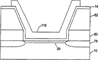
Fig. 8 is the vertical view of example embodiment of the present invention that comprises the integrated reflector 100 of the emitter region 84 in the cathode layer 14.This cathode layer 14 is electrically coupled to and is arranged on the conductive layer 82, and conductive layer 82 is arranged on the insulating barrier 78.Integrated reflector 100 preferably is illustrated as circle, but also can adopt other shape.Owing to do not have discrete edge in the shape, aspect the more uniform electric field of generation, circle is preferred.
Fig. 9 is the sections of integrated reflector 100 example embodiment shown in Figure 8 along the 9-9 line.Substrate 10, preferably conductive layer or heavily doped semiconductor are for the tunnel layer 20 that is arranged in the window of determining in the insulating barrier 78 provides electron source.Cathode layer 14, film conductive layer preferably is arranged on the tunnel layer 20 and partly is arranged on the conductive layer 82, electrically contacts thereby form with conductive layer.Depend on to insulating barrier 78 and conductive layer 82 selected certain materials, can increase adhesive layer 80 alternatively, so that the bonded interface between conductive layer 82 and the insulating barrier 78 is provided.
Figure 10 is the example block diagram of computer 90, and memory 98 and electronic device that this computer 90 comprises microprocessor 96, be coupled to microprocessor 96 are memory device 94 and display device 92.These electronic devices are coupled to microprocessor 96.Microprocessor 96 can be carried out the instruction from memory, so that can transmit data between memory and the electronic device such as memory device 94 and display device 92.Each electronic device comprises integrated circuit, and this integrated circuit has in conjunction with reflector of the present invention, preferably also has the focus device that is used for focusing on from the emission of reflector.Reflector has the electron source layer that is arranged with insulating barrier on it.Insulating barrier has window, and window limits tunnel layer and is fabricated on wherein the electron source layer.It on tunnel layer cathode layer.Preferably but the integrated circuit with reflector has been carried out annealing process alternatively, thus increase the supply that can be tunneling to the electronics of cathode layer from electron source layer.Annealing process has also reduced the contact resistance between each metal level, thereby has improved the conductivity of electronics to reflector.
Figure 11 A-11L shows the exemplary process steps that is used for producing in conjunction with reflector of the present invention.Among Figure 11 A, the mask of being made up of medium or photoresist 102 is used to substrate 10, and substrate 10 is silicon semiconductor substrate preferably, though substrate 10 also can be conductive membrane layer or conductive substrates.The electrical sheet resistance of substrate 10 preferably is about the 100-0.0001 ohmcm.
In Figure 11 B, when substrate 10 was silicon substrate, preferably use oxide growth method formed insulating barrier 78.Insulating barrier 78 can be made up of other oxide, nitride or other conventional medium with deposit alone or in combination of conventional semiconductor technology or growth alternatively.Insulating barrier 78 is formed on the substrate except masked 102 zones that cover.Masked 102 zones of determining, thereby promptly be that the cavity that obtains is the window of determining in the insulating barrier 78, position and the shape of integrated reflector 100 when removing mask 102 that forms after a while determined.
In Figure 11 C, optionally adhesive layer 80 is applied on substrate 10 and the insulating barrier 78.When the conductive layer 82 (seeing Figure 11 D) when being made up of gold of coating after a while, this adhesive layer 80 is tantalum preferably.The deposition technology of handy routine applies this adhesive layer.The thickness of this adhesive layer preferably is about 100-200 , but depends on selected material and can be any thickness.
If in Figure 11 D, conductive layer 82 is applied on the substrate 10 on each layer of previous coating, for example on the adhesive layer 80 that has used.The most handy conventional deposition technology forms conductive layer.This conductive layer preferably thickness is about the gold of 500-1000 .
In Figure 11 E, patterned layer 104 is applied on the conductive layer 82, and forms window therein, so that determine to be used for forming the corrosion area of integrated reflector.This patterned layer 104 preferably thickness is about 1 micron positive light erosion resistant agent layer.
In Figure 11 F, the most handy wet corrosion technique produces the window in patterned layer 104 inner conducting layers 82.This corrosion can produce as directed isotropic etch usually and distribute, wherein the partially conductive layer below patterned layer 104 by undercutting.Used wet corrosion technique is preferably different if the adhesive layer 80 that has used reacts, so that prevent that corrosion material from reaching and substrate 10.Dry corrosion process can be used for corroding this conductive layer 82 alternatively.
In Figure 11 G, the most handy dry corrosion process that adhesive layer 80 is responded produces anisotropy and distributes 108.
In Figure 11 H, on patterned layer 104 on the surface and the window in the insulating barrier 78 of processed substrate 10, coating tunnel layer 20, this tunnel layer 20 is preferably such as metal cluster dielectric, TiO
x, TaO
x, WSiN, TaAlO
xN
y, TaAlO
x, or AlO
xN
yAnd so on but TiO preferably
xHigh dielectric strength material.The most handy splash-proofing sputtering metal is also introduced oxygen and/or the method for nitrogen is come deposit tunnel layer 20, so that form the medium of thickness less than about 500 , this thickness preferably is about 50-250 , for example is about 100 .
In Figure 11 I, stripping technology is used to remove patterned layer 104 and the part tunnel layer 20 that is arranged on the patterned layer 104.Low temperature plasma preferably is used to react the organic material in the corrosion ablation pattern layer 104.In the flat plasma etching process, used gas is oxygen preferably.Processed substrate 10 is placed in the operating room, and introduces oxygen, and oxygen excited by energy source, thereby produces plasma field.Plasma field is activated to upper state with oxygen, and this is oxidized to gas with patterned layer 104 components again, is removed from the operating room by vacuum pump.Since its volume ratio near and difference, so some component of patterned layer 104 in stripping process with the tunnel layer 20 that approaches that is deposited on the patterned layer 104 in component react.For example, from the carbon monoxide of patterned layer 104 releases and the TiO of tunnel layer 20
xOxygen in the layer reacts, and forms carbon dioxide, is eliminated then, stays a spot of Ti on the surface of conductive layer 82.Like this, the tunnel layer 20 that is arranged on the patterned layer 104 has just been removed in stripping technology basically.After stripping technology is finished, only retain tunnel layer 20 parts in the window that is arranged in insulating barrier 78 basically.
The wet method stripping technology can be used for replacing plasma stripping technology alternatively.After tunnel layer 20 was applied to the substrate of handling 10, substrate 10 was immersed in the solvent, and swelling is also removed patterned layer 104, thereby kept the tunnel layer 20 in the window that is arranged in insulating barrier 78.
Figure 11 J shows coating cathode layer 14 on the surface of the substrate of handling 10.Cathode layer 14 is preferably such as the thin film metal layer of platinum, and thickness preferably is about 50-250 .Other metal such as gold, molybdenum, iridium, ruthenium, tantalum, chromium or other refractory metal or its alloy can be used to cathode layer 14.Be arranged in cathode layer 14 on the tunnel layer 20 and constituted emitter surface 86 in the emitter chamber 114.
Figure 11 K shows the coating of negative electrode resist layer 116, and it is coated and graphically to determine that cathode layer 14 treats to be corroded the window at place so that a plurality of reflectors at the bottom of the isolation liner on 10.
Figure 11 L shows cathode layer 14 that had been corroded and the negative electrode resist 116 that is eliminated.It in emitter chamber 114 emitter surface 86.Fig. 8 shows the example top view of the structure that obtains.Emitter surface 86 has first area.Emitter chamber 114 has first alveolus that meets the boundary with emitter surface 86, has sidewall substantially parallel in adhesive layer 80.Emitter chamber 114 has second alveolus that is formed in the conductive layer 82, and its sidewall deflects into the window with second area.This second area is greater than first area.Cathode layer 14 is arranged on the sidewall in first and second districts of emitter surface 86 and emitter chamber 114.Utilize the integrated circuit thin-film technique to make reflector, can be integrated by the traditional active circuit in custom integrated circuit.As mentioned above, the integrated circuit with reflector can be used to display device or memory device.After making, preferably reflector is carried out annealing process, so that increase emission measure from reflector.
Figure 12 A and 12B are the curves that is used for increasing the example annealing process of the emission current capacity that embodies reflector of the present invention.This annealing process has also improved device yield and quality, makes emitter lifetime longer.In other benefit, this annealing process helps to reduce the contact resistance of different metal, thereby increases the electric current that flows to reflector.
In Figure 12 A, first heat distribution 120 showed the substrate that comprises in conjunction with the processing of reflector of the present invention and at first be raised to about 400 ℃ within 10 minute, kept 30 minutes under this temperature then.The substrate of handling was slowly cooled in about 55 minutes then gets back to room temperature (about 25 ℃).
In Figure 12 B, second heat distribution 122 showed the substrate that comprises in conjunction with the processing of reflector of the present invention and be heated to about 600 ℃ temperature within 10 minute, and kept about 30 minutes under this temperature.The substrate of handling then in about 100 minutes by cool to room temperature gradually.The one skilled in the art is understandable that the temperature of lifting and the speed of cooling can be revised and design still according to the invention and scope from described exemplary process.By means of to comprising that at least one anneals in conjunction with the substrate of reflector of the present invention, some characteristics of reflector have been improved.
Claims (20)
1. a reflector (50,100), it comprises:
Electron source (10);
Cathode layer (14); And
Be arranged in the tunnel layer (20) between electron source and the cathode layer, wherein, electron source, cathode layer and tunnel layer have stood annealing process (120,122).
2. the reflector of claim 1 (50,100), wherein, tunnel layer (20) is a metal cluster dielectric.
3. the reflector of claim 1 (50,100), wherein, tunnel layer (20) is to be selected from TiO
x, TaO
x, WSiN, TaAlO
xN
y, TaAlO
x, and AlO
xN
yMetal cluster dielectric.
4. the reflector of claim 1 (50,100) can provide greater than every square centimeter 1 * 10
-2The emission current of A.
5. the reflector of claim 1 (50,100), wherein, the thickness of tunnel layer (20) is about 50-250 .
6. an integrated circuit (52), it comprises:
Substrate (10);
Be arranged in the reflector (50,100) of the claim 1 on the substrate; And
Be used for making the circuit (72) of the reflector work that is produced on the substrate with reflector.
7. electronic device, it comprises:
Claim 1 can emitted energy (22) reflector (50,100); And
Anode construction (76,40,58), it can receive the energy of emission and produce at least the first effect in response to the energy that receives emission and produce second effect in response to receiving the energy of emission.
8. the electronic device of claim 7, wherein, this electronic device is a kind of large scale memory spare (Fig. 7), and anode construction is a kind of storage medium may (58), this electronic device also comprises reading circuit (62), is used for surveying the effect that produces on the anode construction.
9. the electronic device of claim 7, wherein, this electronic device is a kind of display device (Fig. 6), and anode construction is a kind of display screen (40), it produces visible effect in response to the energy that receives emission.
10. the electronic device of claim 9, wherein, display screen (40) comprise can be in response to the energy (22) that receives emission one or more phosphors (42) of ballistic phonon (18).
11. a reflector (50,100), it comprises:
Electron source layer (10);
Be produced on the insulating barrier (78) that on the electron source layer and wherein defines window;
Be produced on the tunnel layer on the electron source layer (20) in the window; And
Be produced on the cathode layer (14) on the tunnel layer;
Wherein, reflector has stood annealing process (120,122), so that increase the supply that is tunneling to the electronics (10) of the cathode layer that is used for energy emission (22) from electron source layer.
12. the reflector of claim 11 (50,100), except electronics (16) emission, can also ballistic phonon (18).
13. the reflector of claim 11 (50,100), wherein, tunnel layer (20) is a metal cluster dielectric.
14. the reflector of claim 11, wherein, cathode layer (14) has the emissivity that is about 0.01A greater than every square centimeter.
15. the reflector of claim 11, wherein, tunnel layer (20) is to be selected from TiO
y, TaO
x, WSiN, TaAlO
xN
y, TaAlO
y, and AlO
xN
yMetal cluster dielectric.
16. the reflector of claim 11, wherein, the thickness of tunnel layer (20) is about 50-250 .
17. the method at electron source (10) last formation reflector (50,100), it comprises the following step:
Coated conductive layer (80,82), so that be adhered to the insulating barrier (78) that is arranged on the electron source (10), this insulating barrier is determined the window to electron source;
On conductive layer, apply patterned layer (104);
In graphical and conductive layer, form window (108) to electron source;
On patterned layer and window, apply tunnel layer (20); And
Etch pattern layer (Figure 11 I) so that remove patterned layer from the tunnel layer below, thereby is removed the tunnel layer that is not arranged in the window with stripping means from conductive layer.
18. the method for claim 17 also comprises the reflector of handling is annealed (120,122) to increase the step of tunnelling current.
19. the method for claim 17, wherein, the thickness of coated tunnel layer (20) is less than about 500 .
20. the method for claim 17 also is included in the step that tunnel layer (20) is gone up coating cathode layer (14).
Applications Claiming Priority (2)
| Application Number | Priority Date | Filing Date | Title |
|---|---|---|---|
| US09/846,127 US6781146B2 (en) | 2001-04-30 | 2001-04-30 | Annealed tunneling emitter |
| US09/846,127 | 2001-04-30 |
Publications (1)
| Publication Number | Publication Date |
|---|---|
| CN1539152A true CN1539152A (en) | 2004-10-20 |
Family
ID=25297021
Family Applications (1)
| Application Number | Title | Priority Date | Filing Date |
|---|---|---|---|
| CNA028133072A Pending CN1539152A (en) | 2001-04-30 | 2002-04-16 | Tunneling emitter |
Country Status (9)
| Country | Link |
|---|---|
| US (3) | US6781146B2 (en) |
| EP (1) | EP1384244B1 (en) |
| JP (1) | JP2005502159A (en) |
| KR (1) | KR20040015202A (en) |
| CN (1) | CN1539152A (en) |
| DE (1) | DE60201748T2 (en) |
| HK (1) | HK1059336A1 (en) |
| TW (1) | TW550621B (en) |
| WO (1) | WO2002089167A2 (en) |
Cited By (1)
| Publication number | Priority date | Publication date | Assignee | Title |
|---|---|---|---|---|
| CN107248489A (en) * | 2016-08-29 | 2017-10-13 | 北京大学 | A kind of surface tunnelling micro electric component and its array and implementation method |
Families Citing this family (14)
| Publication number | Priority date | Publication date | Assignee | Title |
|---|---|---|---|---|
| US6911768B2 (en) * | 2001-04-30 | 2005-06-28 | Hewlett-Packard Development Company, L.P. | Tunneling emitter with nanohole openings |
| US6758711B2 (en) * | 2001-06-14 | 2004-07-06 | Hewlett-Packard Development Company, L.P. | Integrated focusing emitter |
| US6558968B1 (en) * | 2001-10-31 | 2003-05-06 | Hewlett-Packard Development Company | Method of making an emitter with variable density photoresist layer |
| US6703252B2 (en) * | 2002-01-31 | 2004-03-09 | Hewlett-Packard Development Company, L.P. | Method of manufacturing an emitter |
| US6852554B2 (en) | 2002-02-27 | 2005-02-08 | Hewlett-Packard Development Company, L.P. | Emission layer formed by rapid thermal formation process |
| US6841794B2 (en) * | 2003-02-18 | 2005-01-11 | Hewlett-Packard Development Company, L.P. | Dielectric emitter with PN junction |
| KR100935934B1 (en) * | 2003-03-15 | 2010-01-11 | 삼성전자주식회사 | Emitter for electron-beam projection lithography system and method of manufacturing thereof |
| US20040213128A1 (en) * | 2003-04-25 | 2004-10-28 | Marshall Daniel R. | Beam deflector for a data storage device |
| US20040213098A1 (en) * | 2003-04-25 | 2004-10-28 | Marshall Daniel R. | Focus-detecting emitter for a data storage device |
| DE10330571B8 (en) * | 2003-07-07 | 2007-03-08 | Infineon Technologies Ag | Vertical power semiconductor devices with injection damping agent in the edge area and manufacturing method therefor |
| US7187124B2 (en) * | 2004-02-17 | 2007-03-06 | Hewlett-Packard Development Company, L.P. | Transparent electron source emitter device and method |
| US7454221B1 (en) * | 2005-07-12 | 2008-11-18 | Hewlett-Packard Development Company, L.P. | Electron tube amplification |
| US7759747B2 (en) | 2006-08-31 | 2010-07-20 | Micron Technology, Inc. | Tantalum aluminum oxynitride high-κ dielectric |
| US10109794B2 (en) * | 2015-06-08 | 2018-10-23 | SK Hynix Inc. | Semiconductor device including an etching stop layer and method of manufacturing the same |
Family Cites Families (40)
| Publication number | Priority date | Publication date | Assignee | Title |
|---|---|---|---|---|
| US3735186A (en) * | 1971-03-10 | 1973-05-22 | Philips Corp | Field emission cathode |
| NL184589C (en) | 1979-07-13 | 1989-09-01 | Philips Nv | Semiconductor device for generating an electron beam and method of manufacturing such a semiconductor device. |
| GB2109159B (en) | 1981-11-06 | 1985-05-30 | Philips Electronic Associated | Semiconductor electron source for display tubes and other equipment |
| DE3750936T2 (en) | 1986-07-04 | 1995-05-18 | Canon Kk | Electron emitter device and its manufacturing method. |
| JPH02503728A (en) | 1988-03-25 | 1990-11-01 | トムソン‐セーエスエフ | Method for manufacturing a field emission source and its application to manufacturing an emitter array |
| EP0713237B1 (en) | 1989-09-04 | 2000-12-27 | Canon Kabushiki Kaisha | Electron emission element and method of manufacturing the same |
| US5814832A (en) | 1989-09-07 | 1998-09-29 | Canon Kabushiki Kaisha | Electron emitting semiconductor device |
| JPH0512988A (en) | 1990-10-13 | 1993-01-22 | Canon Inc | Semiconductor electron emitting element |
| DE69223707T2 (en) | 1991-09-13 | 1998-05-20 | Canon Kk | Semiconductor electron emitting device |
| US5473218A (en) * | 1994-05-31 | 1995-12-05 | Motorola, Inc. | Diamond cold cathode using patterned metal for electron emission control |
| JP3532275B2 (en) | 1994-12-28 | 2004-05-31 | ソニー株式会社 | Flat display panel |
| US5557596A (en) * | 1995-03-20 | 1996-09-17 | Gibson; Gary | Ultra-high density storage device |
| US5702281A (en) * | 1995-04-20 | 1997-12-30 | Industrial Technology Research Institute | Fabrication of two-part emitter for gated field emission device |
| US5703380A (en) * | 1995-06-13 | 1997-12-30 | Advanced Vision Technologies Inc. | Laminar composite lateral field-emission cathode |
| DE69518849T2 (en) * | 1995-12-14 | 2001-01-11 | Stmicroelectronics S.R.L., Agrate Brianza | Method of manufacturing a microtip cathode structure for a field emission display panel |
| JP3171785B2 (en) * | 1996-06-20 | 2001-06-04 | 富士通株式会社 | Thin display device and method of manufacturing field emission cathode used therefor |
| US5825049A (en) * | 1996-10-09 | 1998-10-20 | Sandia Corporation | Resonant tunneling device with two-dimensional quantum well emitter and base layers |
| JPH10308166A (en) * | 1997-03-04 | 1998-11-17 | Pioneer Electron Corp | Electron emission element and display device using the same |
| US6130503A (en) * | 1997-03-04 | 2000-10-10 | Pioneer Electronic Corporation | Electron emission device and display using the same |
| US5990605A (en) * | 1997-03-25 | 1999-11-23 | Pioneer Electronic Corporation | Electron emission device and display device using the same |
| US6034479A (en) * | 1997-10-29 | 2000-03-07 | Micron Technology, Inc. | Single pixel tester for field emission displays |
| US6011356A (en) | 1998-04-30 | 2000-01-04 | St. Clair Intellectual Property Consultants, Inc. | Flat surface emitter for use in field emission display devices |
| US6137212A (en) | 1998-05-26 | 2000-10-24 | The United States Of America As Represented By The Secretary Of The Army | Field emission flat panel display with improved spacer architecture |
| US6211608B1 (en) * | 1998-06-11 | 2001-04-03 | Micron Technology, Inc. | Field emission device with buffer layer and method of making |
| JP2000011859A (en) | 1998-06-22 | 2000-01-14 | Yamaha Corp | Manufacture of field emission type element |
| US6107732A (en) | 1998-07-13 | 2000-08-22 | Si Diamond Technology, Inc. | Inhibiting edge emission for an addressable field emission thin film flat cathode display |
| US6118136A (en) * | 1998-07-31 | 2000-09-12 | National Science Council Of Republic Of China | Superlatticed negative-differential-resistance functional transistor |
| KR100338140B1 (en) | 1998-09-25 | 2002-05-24 | 이마이 기요스케 | Electric field emission type electron source |
| TW436837B (en) | 1998-11-16 | 2001-05-28 | Matsushita Electric Works Ltd | Field emission-type electron source and manufacturing method thereof and display using the electron source |
| US6328620B1 (en) * | 1998-12-04 | 2001-12-11 | Micron Technology, Inc. | Apparatus and method for forming cold-cathode field emission displays |
| JP3508652B2 (en) | 1999-10-18 | 2004-03-22 | 松下電工株式会社 | Field emission type electron source and method of manufacturing the same |
| JP2001118500A (en) | 1999-10-18 | 2001-04-27 | Matsushita Electric Works Ltd | Electric field radiation electron source and method for fabricating |
| US6765342B1 (en) | 1999-10-18 | 2004-07-20 | Matsushita Electric Work, Ltd. | Field emission-type electron source and manufacturing method thereof |
| KR20010082591A (en) * | 1999-12-21 | 2001-08-30 | 이데이 노부유끼 | Electron emission device, cold cathode field emission device and method for the production thereof, and cold cathode field emission display and method for the production thereof |
| JP3874396B2 (en) * | 2000-01-13 | 2007-01-31 | パイオニア株式会社 | ELECTRON EMITTING ELEMENT, MANUFACTURING METHOD THEREOF, AND DISPLAY DEVICE USING ELECTRON EMITTING ELEMENT |
| EP1146572A3 (en) * | 2000-03-14 | 2005-03-23 | Toyoda Gosei Co., Ltd. | Light source device |
| US6617774B1 (en) * | 2000-04-10 | 2003-09-09 | Hitachi, Ltd. | Thin-film electron emitter device having multi-layered electron emission areas |
| US6815875B2 (en) * | 2001-02-27 | 2004-11-09 | Hewlett-Packard Development Company, L.P. | Electron source having planar emission region and focusing structure |
| US6753544B2 (en) * | 2001-04-30 | 2004-06-22 | Hewlett-Packard Development Company, L.P. | Silicon-based dielectric tunneling emitter |
| US6558968B1 (en) * | 2001-10-31 | 2003-05-06 | Hewlett-Packard Development Company | Method of making an emitter with variable density photoresist layer |
-
2001
- 2001-04-30 US US09/846,127 patent/US6781146B2/en not_active Expired - Lifetime
-
2002
- 2002-04-03 TW TW091106746A patent/TW550621B/en not_active IP Right Cessation
- 2002-04-16 EP EP02723897A patent/EP1384244B1/en not_active Expired - Lifetime
- 2002-04-16 CN CNA028133072A patent/CN1539152A/en active Pending
- 2002-04-16 WO PCT/US2002/012257 patent/WO2002089167A2/en active IP Right Grant
- 2002-04-16 DE DE60201748T patent/DE60201748T2/en not_active Expired - Fee Related
- 2002-04-16 KR KR10-2003-7014149A patent/KR20040015202A/en not_active Application Discontinuation
- 2002-04-16 JP JP2002586371A patent/JP2005502159A/en not_active Withdrawn
-
2004
- 2004-03-23 HK HK04102124A patent/HK1059336A1/en not_active IP Right Cessation
- 2004-05-18 US US10/848,695 patent/US7044823B2/en not_active Expired - Lifetime
- 2004-05-18 US US10/848,754 patent/US20040222729A1/en not_active Abandoned
Cited By (3)
| Publication number | Priority date | Publication date | Assignee | Title |
|---|---|---|---|---|
| CN107248489A (en) * | 2016-08-29 | 2017-10-13 | 北京大学 | A kind of surface tunnelling micro electric component and its array and implementation method |
| CN107248489B (en) * | 2016-08-29 | 2020-03-24 | 北京大学 | Surface tunneling micro electron source, array thereof and implementation method |
| US10804061B2 (en) | 2016-08-29 | 2020-10-13 | Peking University | Surface-tunneling micro electron source and array and realization method thereof |
Also Published As
| Publication number | Publication date |
|---|---|
| US20040222729A1 (en) | 2004-11-11 |
| HK1059336A1 (en) | 2004-06-25 |
| US7044823B2 (en) | 2006-05-16 |
| DE60201748D1 (en) | 2004-12-02 |
| JP2005502159A (en) | 2005-01-20 |
| WO2002089167A2 (en) | 2002-11-07 |
| DE60201748T2 (en) | 2005-12-01 |
| US20040211975A1 (en) | 2004-10-28 |
| TW550621B (en) | 2003-09-01 |
| EP1384244A2 (en) | 2004-01-28 |
| US6781146B2 (en) | 2004-08-24 |
| WO2002089167A3 (en) | 2003-05-01 |
| US20020167001A1 (en) | 2002-11-14 |
| EP1384244B1 (en) | 2004-10-27 |
| KR20040015202A (en) | 2004-02-18 |
Similar Documents
| Publication | Publication Date | Title |
|---|---|---|
| CN1539152A (en) | Tunneling emitter | |
| KR100362377B1 (en) | Field emission devices using carbon nanotubes and method thereof | |
| US6204595B1 (en) | Amorphous-diamond electron emitter | |
| JP2005135930A (en) | Tunneling emitter and forming method | |
| US7170223B2 (en) | Emitter with dielectric layer having implanted conducting centers | |
| CN1522454A (en) | Silicon-based dielectric tunneling emitter | |
| US5556530A (en) | Flat panel display having improved electrode array | |
| US6852554B2 (en) | Emission layer formed by rapid thermal formation process | |
| US6822379B2 (en) | Emission device and method for forming | |
| JP3079086B2 (en) | Method for manufacturing field emission electron source | |
| JP2002539580A (en) | Field emission device and method of use | |
| KR20030025264A (en) | Cold emission cathode and flat display terminal |
Legal Events
| Date | Code | Title | Description |
|---|---|---|---|
| C06 | Publication | ||
| PB01 | Publication | ||
| C10 | Entry into substantive examination | ||
| SE01 | Entry into force of request for substantive examination | ||
| AD01 | Patent right deemed abandoned | ||
| C20 | Patent right or utility model deemed to be abandoned or is abandoned |