CN1228795C - Multilayer transformer having electrical connection in magnetic core - Google Patents
Multilayer transformer having electrical connection in magnetic core Download PDFInfo
- Publication number
- CN1228795C CN1228795C CN00819460.2A CN00819460A CN1228795C CN 1228795 C CN1228795 C CN 1228795C CN 00819460 A CN00819460 A CN 00819460A CN 1228795 C CN1228795 C CN 1228795C
- Authority
- CN
- China
- Prior art keywords
- transformer
- layer
- coil
- primary
- magnetic core
- Prior art date
- Legal status (The legal status is an assumption and is not a legal conclusion. Google has not performed a legal analysis and makes no representation as to the accuracy of the status listed.)
- Expired - Fee Related
Links
- 230000005291 magnetic effect Effects 0.000 title claims abstract description 149
- 238000004519 manufacturing process Methods 0.000 claims abstract description 12
- 239000010410 layer Substances 0.000 claims description 162
- 230000004907 flux Effects 0.000 claims description 44
- 239000000463 material Substances 0.000 claims description 20
- 239000000919 ceramic Substances 0.000 claims description 18
- 229910000859 α-Fe Inorganic materials 0.000 claims description 16
- 239000011229 interlayer Substances 0.000 claims description 15
- XLOMVQKBTHCTTD-UHFFFAOYSA-N Zinc monoxide Chemical compound [Zn]=O XLOMVQKBTHCTTD-UHFFFAOYSA-N 0.000 claims description 9
- 239000003302 ferromagnetic material Substances 0.000 claims description 7
- 229910010293 ceramic material Inorganic materials 0.000 claims description 6
- 229910052797 bismuth Inorganic materials 0.000 claims description 3
- JCXGWMGPZLAOME-UHFFFAOYSA-N bismuth atom Chemical compound [Bi] JCXGWMGPZLAOME-UHFFFAOYSA-N 0.000 claims description 3
- 239000010419 fine particle Substances 0.000 claims description 3
- 239000011787 zinc oxide Substances 0.000 claims description 3
- LWFZQIXVMAHQKA-UHFFFAOYSA-N copper zinc iron(2+) nickel(2+) oxygen(2-) Chemical compound [O-2].[Fe+2].[Zn+2].[Cu+2].[Ni+2].[O-2].[O-2].[O-2] LWFZQIXVMAHQKA-UHFFFAOYSA-N 0.000 claims description 2
- UQSXHKLRYXJYBZ-UHFFFAOYSA-N iron oxide Inorganic materials [Fe]=O UQSXHKLRYXJYBZ-UHFFFAOYSA-N 0.000 claims 2
- 229910001308 Zinc ferrite Inorganic materials 0.000 claims 1
- 238000002955 isolation Methods 0.000 abstract description 3
- 239000011162 core material Substances 0.000 description 62
- 238000009413 insulation Methods 0.000 description 16
- 230000008878 coupling Effects 0.000 description 15
- 238000010168 coupling process Methods 0.000 description 15
- 238000005859 coupling reaction Methods 0.000 description 15
- 238000005516 engineering process Methods 0.000 description 9
- 238000000034 method Methods 0.000 description 8
- 239000011701 zinc Substances 0.000 description 7
- 230000008901 benefit Effects 0.000 description 6
- 239000004020 conductor Substances 0.000 description 6
- 230000037361 pathway Effects 0.000 description 6
- 230000008859 change Effects 0.000 description 4
- 230000015572 biosynthetic process Effects 0.000 description 3
- 230000015556 catabolic process Effects 0.000 description 3
- 239000002245 particle Substances 0.000 description 3
- 230000004888 barrier function Effects 0.000 description 2
- 238000010292 electrical insulation Methods 0.000 description 2
- 230000005611 electricity Effects 0.000 description 2
- 230000004048 modification Effects 0.000 description 2
- 238000012986 modification Methods 0.000 description 2
- SWELZOZIOHGSPA-UHFFFAOYSA-N palladium silver Chemical compound [Pd].[Ag] SWELZOZIOHGSPA-UHFFFAOYSA-N 0.000 description 2
- BASFCYQUMIYNBI-UHFFFAOYSA-N platinum Chemical compound [Pt] BASFCYQUMIYNBI-UHFFFAOYSA-N 0.000 description 2
- 230000008569 process Effects 0.000 description 2
- 238000005245 sintering Methods 0.000 description 2
- 238000004804 winding Methods 0.000 description 2
- 229910021124 PdAg Inorganic materials 0.000 description 1
- BQCADISMDOOEFD-UHFFFAOYSA-N Silver Chemical compound [Ag] BQCADISMDOOEFD-UHFFFAOYSA-N 0.000 description 1
- 238000006243 chemical reaction Methods 0.000 description 1
- 238000004891 communication Methods 0.000 description 1
- 230000006378 damage Effects 0.000 description 1
- 230000000694 effects Effects 0.000 description 1
- 230000005684 electric field Effects 0.000 description 1
- 230000007613 environmental effect Effects 0.000 description 1
- 239000003822 epoxy resin Substances 0.000 description 1
- 230000014509 gene expression Effects 0.000 description 1
- 239000003292 glue Substances 0.000 description 1
- 238000010438 heat treatment Methods 0.000 description 1
- 230000006872 improvement Effects 0.000 description 1
- 239000012535 impurity Substances 0.000 description 1
- 239000012212 insulator Substances 0.000 description 1
- 239000000615 nonconductor Substances 0.000 description 1
- 238000005457 optimization Methods 0.000 description 1
- 230000035699 permeability Effects 0.000 description 1
- 239000004033 plastic Substances 0.000 description 1
- 229920003023 plastic Polymers 0.000 description 1
- 229910052697 platinum Inorganic materials 0.000 description 1
- 229920000647 polyepoxide Polymers 0.000 description 1
- 238000007789 sealing Methods 0.000 description 1
- 239000004065 semiconductor Substances 0.000 description 1
- 229910052709 silver Inorganic materials 0.000 description 1
- 239000004332 silver Substances 0.000 description 1
- 238000005728 strengthening Methods 0.000 description 1
- 239000002966 varnish Substances 0.000 description 1
Images


Classifications
-
- H—ELECTRICITY
- H01—ELECTRIC ELEMENTS
- H01F—MAGNETS; INDUCTANCES; TRANSFORMERS; SELECTION OF MATERIALS FOR THEIR MAGNETIC PROPERTIES
- H01F1/00—Magnets or magnetic bodies characterised by the magnetic materials therefor; Selection of materials for their magnetic properties
- H01F1/01—Magnets or magnetic bodies characterised by the magnetic materials therefor; Selection of materials for their magnetic properties of inorganic materials
- H01F1/03—Magnets or magnetic bodies characterised by the magnetic materials therefor; Selection of materials for their magnetic properties of inorganic materials characterised by their coercivity
- H01F1/12—Magnets or magnetic bodies characterised by the magnetic materials therefor; Selection of materials for their magnetic properties of inorganic materials characterised by their coercivity of soft-magnetic materials
- H01F1/34—Magnets or magnetic bodies characterised by the magnetic materials therefor; Selection of materials for their magnetic properties of inorganic materials characterised by their coercivity of soft-magnetic materials non-metallic substances, e.g. ferrites
- H01F1/342—Oxides
- H01F1/344—Ferrites, e.g. having a cubic spinel structure (X2+O)(Y23+O3), e.g. magnetite Fe3O4
-
- H—ELECTRICITY
- H01—ELECTRIC ELEMENTS
- H01F—MAGNETS; INDUCTANCES; TRANSFORMERS; SELECTION OF MATERIALS FOR THEIR MAGNETIC PROPERTIES
- H01F27/00—Details of transformers or inductances, in general
- H01F27/28—Coils; Windings; Conductive connections
- H01F27/2804—Printed windings
-
- H—ELECTRICITY
- H01—ELECTRIC ELEMENTS
- H01F—MAGNETS; INDUCTANCES; TRANSFORMERS; SELECTION OF MATERIALS FOR THEIR MAGNETIC PROPERTIES
- H01F17/00—Fixed inductances of the signal type
- H01F17/04—Fixed inductances of the signal type with magnetic core
-
- H—ELECTRICITY
- H01—ELECTRIC ELEMENTS
- H01F—MAGNETS; INDUCTANCES; TRANSFORMERS; SELECTION OF MATERIALS FOR THEIR MAGNETIC PROPERTIES
- H01F17/00—Fixed inductances of the signal type
- H01F17/0006—Printed inductances
- H01F17/0013—Printed inductances with stacked layers
- H01F2017/002—Details of via holes for interconnecting the layers
-
- H—ELECTRICITY
- H01—ELECTRIC ELEMENTS
- H01F—MAGNETS; INDUCTANCES; TRANSFORMERS; SELECTION OF MATERIALS FOR THEIR MAGNETIC PROPERTIES
- H01F17/00—Fixed inductances of the signal type
- H01F17/0006—Printed inductances
- H01F2017/0066—Printed inductances with a magnetic layer
-
- H—ELECTRICITY
- H01—ELECTRIC ELEMENTS
- H01F—MAGNETS; INDUCTANCES; TRANSFORMERS; SELECTION OF MATERIALS FOR THEIR MAGNETIC PROPERTIES
- H01F27/00—Details of transformers or inductances, in general
- H01F27/28—Coils; Windings; Conductive connections
- H01F27/2804—Printed windings
- H01F2027/2809—Printed windings on stacked layers
Abstract
The present invention provides a manufacturing method for a multi-layer transformer (132), a device and a finished product. The present invention comprises a magnetic core of a transformer formed from a plurality of layers (168 to 174) arranged in a magnetic core region (114) of each layer, wherein the transformer has primary coils (126, 128) arranged on at least one layer and secondary coils (178, 180) arranged on at least on layer; a multi-interconnection passages (130) are connected with the primary coils among the layers, and a second multi-interconnection passage (130) is connected with the secondary coils among the layers. The interconnection passages are arranged in the center of the transformer adjacent to the magnetic core; in such a way, the whole volume, the size, the weight and the cost of the transformer are reduced, and the transformer accords with the requirement of standard isolation safety.
Description
Technical field
The present invention relates to transformer, more specifically, relate to multi-layer ceramics transformer and method.
Background technology
Traditional transformer device structure comprises that coil and the magnetic force that is called magnetic core see through the zone.Coil is made up of insulated conductor usually and is wrapped on the magnetic core usually.Coil also can be wrapped on the bobbin of insulation, and bobbin is then placed around magnetic core.Transformer is usually formed primary coil and secondary coil by several coils that promptly enclosed by different circles.
Traditional transformer has the separate magnetic cores and the coil region of long merging, makes them suffer restraints with regard to relative magnetic core is placed coil.Usually, coil is wrapped on the magnetic core, has increased the whole dimension and the volume of transformer like this.Adopting current constructing technology is coil unpractical by magnetic core physically.Do the very high spended time again of cost like this.In addition, great majority will be induced unwanted magnetic field except the magnetic field of the generation that designs by possible the circuit of core material.So, limited the choice of reducing the traditional transformer size around magnetic core zone coil.The size that reduces insulating transformer usually is difficult, because the physical size of insulating transformer and structure have played effect in its electrical insulation characteristics.
Except physical size limitations, be generally used for the also essential compliant safety standard of transformer that telecommunications is used, because they are widely used in user's electronic equipment and communication network are isolated, for example telephone network.The instrument of many standards (agency) needs transformer that the certain voltage insulation barrier is provided and meets gap (clearance) distance and electric leakage (creepage) distance of needs in the transformer.
Clearance distance is defined as the beeline between two conductive components measuring by air, and particular importance, though because air is good insulator, under enough strong electric field with final ionization and destruction insulation barrier.
Leakage distance, be defined as the beeline between two conducting parts measuring along insulating surface, also particular importance, because under suitable environmental condition and time enough, give enough electromotive forces between two points of insulating surface, insulating surface is will be final breakdown and cause destroying its insulation characterisitic.
By the use insulating tape, the crossover band, varnish, epoxy resin, insulated wire and plastics bobbin are made the insulation needs that traditional transformer meets distance and voltage.Use the various combinations of these materials to guarantee that transformer will withstand required voltage and puncture restriction and predetermined distance.
Except physical size limitations and electrical insulation characteristics restriction, traditional transformer is difficult to automated manufacturing.Because need be welded to the bobbin terminal to coil the end of a thread, traditional wire-wound transformer is difficult to automated manufacturing.In addition, winding around and make their separated from each other difficult in manufacturing process, and need many hand assembled work.May need the technology of adding and cause the cost of transformer to surpass the bearing value in market for the simple change of the industry standard of higher insulation voltage.
In order to overcome the restriction of traditional transformer, disclosed the method for many manufacturing ceramic transformers.These ceramic transformer great majority are not emphasized electricity isolation needs, provide the physics needs of abundant voltage breakdown protection such as needs.
In addition, the ceramic transformer that meets security needs does not usually usually provide sufficient performance, such as the bad coupling between the coil of conventional ceramic transformer.
Like this, on technology, need improved transformer and method, particularly, low cost, undersized ceramic transformer is easy to large quantities of automated manufacturings and also compliant security needs.
Summary of the invention
In order to overcome the restriction on above-mentioned prior art, and overcome other and can clearly limit when reading and understanding specification of the present invention, the method and apparatus that the present invention discloses provides the multi-layer transformer that reduces physical size and volume and can influence its electric isolation characteristic sharply.
In one embodiment, the present invention has disclosed a transformer that the sandwich tape structure is arranged, the sandwich tape structure comprises a plurality of layers, it defines the magnetic core zone that is arranged on wherein two layers that form magnetic core of transformer at least, primary coil is arranged on one of them layer, secondary coil is arranged on one of them layer, more than first interconnection vias is connected the primary coil of interlayer, more than second interconnection vias is connected the secondary coil of interlayer, and wherein first and second interconnection vias are arranged near the magnetic core of transformer center.
In another embodiment of the present invention, these layers are by concurrent roasting-ceramic material manufacturing.
Still in one embodiment, the concurrent roasting ceramic material is low temperature-concurrent roasting-pottery (LTCC) material.
In another embodiment, concurrent roasting-ceramic material is high temperature concurrent roasting-pottery (HTCC) material.
An advantage of the invention is the volume that has reduced whole transformer, and the material quantity of making transformer and needing reduced also, this has obviously reduced the whole cost and the weight of transformer.
The present invention also provides the multi-layer transformer that the interlayer cross coil is arranged.In one embodiment, multi-layer transformer comprises a plurality of layers, it has defined the formation that is arranged at least wherein on two layers magnetic core zone of magnetic core of transformer, primary coil is arranged on the ground floor, secondary coil is arranged on the second layer, arrange close to each otherly for first and second layers, primary coil and secondary coil are arranged with the interlayer cross reference from one deck to another layer like this.
Still in one embodiment, transformer also comprises more than second interconnection vias of secondary coil between the interconnection vias of primary coil between more than first articulamentum and articulamentum.
In one embodiment, first and second interconnection vias are arranged in extremely near the magnetic core of transformer center.
In addition in one embodiment, the starting end of primary coil and end are held in the same end layer of the multilayer that is arranged in transformer one end.
Still in one embodiment, the starting end of the secondary coil of multi-layer transformer and end end are arranged in a plurality of layers same side layer of transformer one end.
Still in one embodiment, the starting end of the primary coil of multi-layer transformer and secondary coil and end end are arranged in a plurality of layers same end layer of transformer one end.
In one embodiment, the multilayer of transformer is ferromagnet concurrent roasting-pottery band.Concurrent roasting-pottery is with by low temperature concurrent roasting-ceramic making (LTCC).
In another embodiment, concurrent roasting-pottery is with by high temperature concurrent roasting-pottery (HTCC) material.
Still in one embodiment, the primary and secondary coil is the primary and secondary electrical conductivity component at least the first and second layers that are arranged in separately in the magnetic core, by an end of the primary electrical transport element on ground floor being connected to second end of the secondary electrical transport element of one deck wherein at the path of first and second interlayers, first and second layers adjacent to each other, electrical conductivity component is usually perpendicular to the magnetic flux line of magnetic core, a part first electrical conductivity component that is arranged on the most close path is parallel to second electrical conductivity component that is arranged on the most close path, these two parts have been eliminated the magnetic effect around path so basically at the electric current that opposite direction conduction equates.
In addition in one embodiment, the primary and secondary coil that is arranged on the adjacent layer is separated by first distance, and first distance is less than second distance, and this second distance is the spacing between two adjacent parts of the primary electrical transport element of primary coil on the identical layer.
In addition in one embodiment, be arranged on the adjacent layer the primary and secondary coil by first distance separately, first distance is less than second distance, this second distance is the spacing between two adjacent parts of the secondary electrical transport element in the secondary coil on identical layer.
In addition in one embodiment, the primary and secondary coil that is arranged on the adjacent layer is separated by first distance, and first distance is less than second distance, and this second distance is the spacing between primary and secondary coil primary and secondary electrical conductivity component separately.
In addition in one embodiment, primary coil is a spiral type.
In addition in one embodiment, secondary coil is a spiral type.
Also in one embodiment, the primary coil that is arranged on the ground floor at least produces primary magnetic flux, and the secondary coil that is arranged on the secondary layer at least is coupled on the primary coil by primary magnetic flux.
An advantage of the invention is that the magnetic flux line from transformer can not change significantly, because the net current in first and second electrical conductivity components of path is zero.Therefore, there is not tangible stray magnetic field to be incorporated into the magnetic core of transformer zone.
Another advantage of the present invention is that the magnetic coupling between coil is improved significantly.
The present invention also provides the multi-layer transformer of balance.In one embodiment, transformer comprises at least one deck and is furnished with coil on one deck at least at this, and coil produces magnetic flux, forms the magnetic core zone by coil, and the magnetic core zone is substantially perpendicular to magnetic flux.At the top layout flat board of one deck at least, flat board provides the return path to magnetic flux, and wherein the total dull and stereotyped transverse cross-sectional area that is covered by magnetic flux is more equal substantially than the magnetic core zone that is covered by magnetic flux.
The present invention also provides the multi-layer transformer of balance.In one embodiment, transformer comprises at least one deck and is furnished with coil on one deck at least at this, and coil produces magnetic flux, forms the magnetic core zone by coil, and the magnetic core zone is substantially perpendicular to magnetic flux.At the top layout flat board of one deck at least, flat board provides the return path to magnetic flux, and wherein the total dull and stereotyped transverse cross-sectional area that is covered by magnetic flux is bigger than the magnetic core zone that is covered by magnetic flux.
The balancing transformer that an advantage of the invention is has realized having the balance transverse cross-sectional area, like this for the magnetic density maximum of intended size.
The present invention also provides the ferromagnetic material that is used for ceramic transformer.In one embodiment, material comprises nickel-copper-zinc-iron oxide (NiCuZnFeO), and wherein ferrite (FeO) content is the 40%-60% of total WT%.Ferromagnetic material also comprise quantity just 1% the bismuth (Bi) of total (weight) Wt% and quantity be 10% the zinc oxide (ZnO) of total amount Wt%, wherein after roasting the zinc oxide fine particles size of ceramic transformer less than 10 μ m.
These innovation advantage and features with various other expressions characteristic of the present invention are pointed out by claim additional and that form a specification part.But, in order to understand the present invention better, its advantage and adopt its resulting product, and follow the problem of description, the accompanying drawing of having made an other formation specification part has wherein illustrated and has described the specific examples of device as a reference according to the present invention.
Description of drawings
With reference now to accompanying drawing,, wherein identical reference number is represented corresponding part always:
Figure 1A, B show the side view and the cross-sectional view of conventional wire-wound transformer.
Fig. 2 illustrates the multi-layer transformer top floor plan view of the preferred embodiment according to the present invention.
Fig. 3 illustrates the transformer coil layer that is illustrated in electric current in the polarity of the preferred embodiment according to the present invention.
Fig. 4 be according to the present invention preferred embodiment be illustrated in another transformer coil layer in Fig. 3 relative polarity.
Fig. 5 is two the transformer coil layers shown in Fig. 3 and 4 in the heap formula is arranged shown in the preferred embodiment according to the present invention, have further described electric current and corresponding magnetic flux line at each layer.
Fig. 6 A, B are illustrated in the magnetic flux line path of the separative primary and secondary coil on conventional multi-layer transformer one deck.
Preferred embodiment is illustrated in extremely near the magnetic flux line path and first and second coils on the multi-layer transformer separating layer according to the present invention for Fig. 7 A, B.
Preferred embodiment illustrates the one deck of multi-layer transformer and the plane graph of transverse cross-sectional area according to the present invention for Fig. 8 A, B.
Fig. 9 illustrates the part exploded view of the multi-layer transformer of the preferred embodiment according to the present invention.
Figure 10 illustrates the zone of the balance multi-layer transformer of the preferred embodiment according to the present invention.
Preferred embodiment illustrates the plane graph of three examples of different helical coil patterns according to the present invention for Figure 11 A, B and C.
Embodiment
The invention provides the transformer of sandwich tape structure.The present invention also provides the multi-layer transformer of the primary and secondary coil of interconnected relationship coupling.The present invention also provides the balance multi-layer transformer.In addition, the invention provides the ferromagnetic material that is used for transformer.
In the preferred embodiment that is described below, carried out forming the quoting of accompanying drawing of a specification part, wherein illustrated by implementing specific embodiment of the present invention.Be appreciated that and when not deviating from the scope of the invention, can use other embodiment and can make the change of manufacturing structure.
Figure 1A illustrates the side view of conventional transformer, has described to have to begin to go between 46 and the coil of end leads 48, and their twine insulation bobbin 44 several times.Coil comprises insulated conductor.Electric current by coil 46 and 48 has produced magnetic field.Magnetic flux line is perpendicular to coil.By allowing magnetic flux line by low magnetic resistance is arranged, promptly the core 42 of the Tou Guoed magnetic of resistance is set up magnetic flux line with the magnetic flux line that this method produces, and is promptly strengthening of concentrating.In order further to guarantee low magnetic resistance, in magnetic core 42, set up the magnetic-path 40 of sealing.Usually other example of conventional transformer has two or more coils, comprises the coil of primary and secondary, needs at least four pigtail splices to magnetic core.
Figure 1B illustrates the profile of the transverse cross-sectional area A-A of conventional transformer among Figure 1A.The magnetic core transverse cross-sectional area is perpendicular to magnetic flux line path 40 (Figure 1A).The whole dimension of optimization magnetic core transverse cross-sectional area 42 mates the best magnetic flux density specification of core material and such as the electricity needs in the application of inductance, this is important.Comprise that also the coil that further describes and clarify to coil region 50 is wrapped in coil magnetic core 42 parts and the core by magnetic core 42 not.
Fig. 2 illustrates the top layer of the multi-layer transformer of preferred embodiment according to the present invention.The top layer 61 of multi-layer transformer can comprise wiring pad and four conduction clear openings of four conductions, is called passage 60.The wiring pad of conduction begins lead-in wire and primary coil end leads 52,54 corresponding to primary coil separately.The wiring pad 56,58 of other conduction begins lead-in wire and secondary coil end leads corresponding to secondary coil separately.All layers of head slab 61 and back can be made by the ferrite carrying material, such as low temperature cofire pottery (LTCC) material or high temperature cofire pottery (HTCC) material, or the like.By the conduction path 60 primary and secondary coil of between which floor, can arranging and interconnect.The beginning of main and secondary coil and end leads stop on dull and stereotyped 61 outer surface 63.Conduction pathway 60 common interior sections towards flat board 61.In this embodiment, on identical flat board, arrange the wiring pad that is used for primary coil and secondary coil.The wiring pad that is appreciated that primary coil and secondary coil can be arranged on the different dull and stereotyped or layers.
In Fig. 3, show multi-layer transformer according to preferred embodiment of the present invention.The printed, conductive material forms electrical conductivity component or coil 62 on ferrite tape base layer.Electric current flow through coil 62 produce perpendicular to and around the magnetic field 64 of coil 62.Determine the polarity in magnetic field 64 by sense of current.Each layer in succession of multi-layer transformer has similar coil.Each coil has one or more to have starting end and finishes the circle of end and be electrically connected to conductive wires pad 52,54,56 by conduction pathway 60, or 58 (Fig. 2).Be appreciated that the number of turn of determining each primary and secondary coil by given transformer specification.Coil 62 is divided into inner core part 68 and external magnetic core segment 66 to ferrite basic unit.Conduction pathway 60 preferably is positioned at the size that inner core part 68 reduces transformer.Be appreciated that passage or several passage can be disposed in the outside of inner core 68.Therefore, in a preferred embodiment, all conduction pathways can pass to adjacent layer 74 (Figure 4 and 5) by inner core part 68 from layer 76.Utilize passage 60 conductive coil 62 that interconnects to reduce the whole volume of transformer significantly and can influence the magnetic property of transformer sharply by inner core part 68.
Fig. 4 shows the layer 74 of the multi-layer transformer of the preferred embodiment according to the present invention.Conductive coil 72 is printed onto on the ferrite tape base layer.Electric current flow through coil 72 produce perpendicular to and the magnetic field 70 of wound coil 72.Determine that by sense of current the polarity in magnetic field 70 and it are opposite with the polarity that goes up the magnetic field 64 (Fig. 3) that produces at transformer adjacent layer 76 (Fig. 3).Coil 72 has one or more circles.The starting end of coil and end end can be electrically connected to the conductive wires pad 52,54,56 by conduction pathway 60, or 58 (Fig. 2).Coil 72 is divided into inner core part 69 and external magnetic core segment 67 to the ferrite tape base layer of layer 74.Conduction path 60 preferably is positioned at inner core part 69.Therefore, all conduction paths can be by 76 the inner core part 69 from layer 74 to layer.Similarly, determine the number of turn of each primary and secondary coil by given transformer specification.
According to this preferred embodiment of the present invention, Fig. 5 further illustrates the layer 76 and the layer 74 of multi-layer transformer.Layer 76 and 74 can be two adjacent layers of multi-layer transformer, or the transformer of two layers.The conductive coil 62 of layer 76 is electrically connected to the conductive coil 72 of layer 74 by adopting conduction path 60.Electric current flows through coil 62, has produced magnetic field 64, and magnetic field is opposite with the polarity in the magnetic field 70 that is produced by the conductive coil on the layer 74 72. Magnetic field 64 and 70 polarity have been surrounded a part of conductive coil 62 and 72, and polarity is positioned at the middle magnetic core zone of transformer, cancels each other thereby direction is opposite each other.So, be zero in the clean magnetic field of magnetic core regional center.These characteristics make the interconnection coil can influence its magnetic characteristic when regional by middle the magnetic core of multi-layer transformer sharply.In addition, the whole volume of transformer and cost also can reduce.
This preferred embodiment of the present invention provides balance, multi-layer transformer, and meet the safety standard or the needs of puncture voltage.Some that will connect transformer between user's equipment and telephone wire may be up to the insulation protection of 1500VAC in using.Insulation voltage between primary coil and secondary coil usually needs about 1.6 times value and does not have many electric leakages to pass through transformer.In a preferred embodiment, multi-layer transformer can comprise that thickness is 0.0035 inch layer.The thickness of layer is substantially equal to the distance between primary coil and the secondary coil.Layer thickness is the magnetic coupling that well obtains in coil and function compromise between the enough insulation protection is provided.For example, between coil than the good insulating of thick-layer than thinner layer.But, because coil further separates, so to poor than the magnetic coupling on the magnetic coupling comparison thinner layer of thick-layer.
In order to improve magnetic coupling and the insulation characterisitic between the primary and secondary coil in multi-layer transformer, the present invention also provides improved material for transformer.In a preferred embodiment, material includes the Ni ferrite stock (NiCuZnFeO) of the ferrite (FeO) of about 50% weight.In order to increase insulation protection is insulation voltage, and the Bi that exists in the synthetic of base material will be reduced to trace and the degree of Zn has also reduced.Base material is semiconductor substantially.By reducing the Zn content in synthetic, and the Zn particle is worn into diameter dimension less than 5-10 μ m, the threshold voltage that obtains is thus controlled electric leakage, and to flow to acceptable degree be sufficiently high.The actual percentage content of the Zn that uses in the synthetic depends on such as Zn mean particle dia size, the amount of impurities in synthetic, and the factor of the whole thickness between the primary and secondary coil of transformer layer and so on.For example, thickness is arranged is among 0.0035 inch the embodiment preferable, Zn content less than Wt% (percentage by weight) 10% and less than 4% of At% (atomic weight percentage).Be appreciated that and use different layer thicknesses based on the required minimum insulation voltage of application-specific with leakage current.In order to meet different needs, Zn mean particle dia size, percentage composition and layer thickness can be made corresponding adjustment or change within the scope of the present invention.
Usually, the coupling coefficient between the single coil of improvement transformer also needs to control the physical Design of single coil.In Fig. 3-5, described the thickness by reducing each ceramic layer and be close together physically by a middle magnetic core zone coil that is coupled.Coil leans on closely more, and is just many more by the magnetic flux line of each coil, thus the better conversion that has increased the coupling coefficient of transformer and produced the signal of telecommunication.
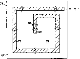
Fig. 6 A and B show the sectional drawing and the cross-sectional view of the conventional transformer 96 of long magnetic circuit 98, and cause the bad coupling between primary coil 100 and secondary coil 102.Fig. 6 B further illustrates primary coil 100 to the distance X that must keep preventing insulation breakdown between the secondary coil 102.In the transformer of routine, X also is the distance between two coils on the identical layer.
According to this preferred embodiment of the present invention, Fig. 7 A and B illustrate the enlarged drawing and the cross-sectional view of transformer 110.In this transformer, show shorter magnetic circuit 112, it has caused the good coupling between primary coil 182 and secondary coil 184.In this preferred embodiment of the present invention, arrange the design of primary and secondary coil, make the magnetic flux line 112 of maximum number from the magnetic core regional center by primary coil 182 and be coupled on the secondary coil 184.As Fig. 7 A, the pattern of the good coupling shown in the B can intersect primary coil 182 and secondary coil 184 by interlayer and obtain.In addition, each coil 182,184 has spiral type to keep the transformer device structure of balance and the distance between coil is reduced to minimum.In one embodiment, coil can be annular angle straight line spiral pattern arranged or the curve spiral pattern.Fig. 7 A further shows the flat board 118 that is installed in main or secondary wire ring layer top.
In addition, in this preferred embodiment according to the present invention, distance Y will be selected less than distance X (Fig. 6 B).The scope of distance X (Fig. 6 B) is from 0.005 inch to 0.100 inch, and scope can be from 0.006 inch to 0.050 inch in a preferred embodiment, and scope can be from 0.006 inch to 0.010 inch in the another one preferred embodiment.Distance Y, just, the vertical interval in any two adjacent windings is chosen as less than X (Fig. 6 B) and optimizes electric insulation and magnetic coupling characteristic.Coil is near more, and it is strong more to be coupled.
Fig. 8 A illustrates the plane graph of the transformer layer 122 that magnetic core zone 114 is arranged that is formed by coil 120.Fig. 8 B illustrates the sectional drawing of which floor transverse cross-sectional area of multi-layer transformer according to this preferred embodiment of the present invention.In Fig. 8 B, show primary coil layer 158,162 and primary coil separately 159,161, secondary wire ring layer 160,164 and secondary coil separately 161,165, head slab 156 and base platform 166.
Fig. 9 is the enlarged drawing of multilayer balancing transformer 132, shows end cover (top layer) 124, bottom cover (bottom) 176, the primary coil layer 168,170 of primary coil 126 and 128 is arranged respectively and the secondary wire ring layer 172 of secondary coil 178 and 180 is arranged respectively, 174 and conduction path 130.In this preferred embodiment according to the present invention, primary coil layer 168 and 170 piles up on the adjacent layer alternately.Primary coil 126 and 128 is basically in separately top alignment.Similarly, secondary wire ring layer 172 and 174 heaps are to the adjacent layer that replaces.Secondary coil 178 and 180 is arranged in top alignment separately basically.In addition, primary coil 126 and 128 and secondary coil 178 and 180 be arranged on the different layers with the interlayer cross reference, and mutually aim at the best magnetic coupling that reaches in multi-layer transformer basically.There are many layouts every handing over layer primary and secondary coil to be appreciated that.
As an example, table 1 shows six kinds of various combinations that can be used for interlayer intersection primary and secondary coil, and wherein coil has the different numbers of turn.In table 1, " P/x " refers to that total primary turns and " S/x " refer to total number of secondary turns, and wherein x is total number of turn of that coil.
Table 1
| Combination | 1 | 2 | 3 | 4 | 5 | 6 |
| P/1 | S/2 | P/2 | S/4 | P/4 | S/6 | |
| S/1 | P/1 | S/1 | P/2 | S/2 | P/3 | |
| S/2 | P/2 | S/2 | P/2 | S/3 | ||
| P/2 | S/2 | P/3 | ||||
| S/4 | P/4 | S/3 | ||||
| P/3 | ||||||
| S/6 |
Be appreciated that and use many other to arrange interlayer intersection primary and secondary coil.
Figure 10 is the plane graph of transformer layer 116 that several transverse cross-sectional area sectional drawings of multi-layer transformer are shown.Figure 10 illustrates inner core zone 214, two side regions 218 of total head slab, the outer cross zone 222 of the zone of conductive coil 220 and layer 216.All 4 sides (having only both sides to illustrate) that comprise head slab zone 218 by the head slab transverse cross-sectional area of magnetic flux line covering.
Parameter shown in Figure 10 has been determined the whole inductance of transformer.Can calculate inductance with following formula:
L=(0.4πN
2Aμ)/l
·10
8
Wherein N is the number of turn of being determined by coil, and A is an inner core cross-sectional area 214, and μ is the permeability of magnetic core, and l is the average length of magnetic path.The entire cross section zone of multi-layer transformer of the present invention is a balance, like this, makes magnetic field reach maximum to given transformer size.The magnetic core transverse cross-sectional area of balance provides the transformer of balance, because return by dull and stereotyped transverse cross-sectional area when magnetic flux line, during by the transformer layer with by the backspace of magnetic core of transformer transverse cross-sectional area, magnetic circuit does not suffer restraints in any direction.
In a preferred embodiment, the magnetic core zone 214 that the total dull and stereotyped transverse cross-sectional area 218 that is covered by magnetic flux line comprises all four sides and is substantially equal to be covered by magnetic flux line.
In another embodiment, the total dull and stereotyped transverse cross-sectional area 218 that is covered by magnetic flux line comprises four all sides and greater than the magnetic core zone 214 that is covered by magnetic flux line.
Figure 11 A, B is the plane graph of three different coil pattern of this preferred embodiment according to the present invention with C.These patterns are straight line spiral patterns 148, and the straight line spiral pattern 150 and the curve spiral pattern 154 of annular angle 152 arranged.There are the straight-line pattern 150 and the curve pattern 154 of annular angle to help reduce micro-capacitance by the master plate zone that when the required number of turn is provided, reduces helical coil.In manufacture process, round angle or curve spiral also help to reduce the electric possibility of weak point between two conductive segment of coil.
Conventional wire-wound transformer shown in Figure 1A and the B has long separate magnetic cores 42 (Figure 1A) and coil region 50 (Figure 1B).Magnetic core 42 (Figure 1A) placement coil is difficult relatively.In this preferred embodiment of the present invention, these restrictions have been overcome, with conductive coil 62,72 (Fig. 5) are by conduction pathway 60 (Fig. 2,3,4,5) and the center magnetic core zone 68 by the multi-layer ceramics transformer, 69 (Fig. 3 and 4) obtain compact size, good inductance coupling high between coil, and satisfied safety regulation.
This preferred embodiment of the present invention can be used the concurrent roasting ceramic technology.An example is to use low temperature concurrent roasting ceramic technology (LTCC).Another example is to use high temperature concurrent roasting ceramic technology (HTCC).Magnetic core and electrical insulator are cast into a band and make by a kind of Ferrite Material.If required, band cuts into the thin slice that comprises location hole basically.The passage that uses as the interlayer conductive interconnect can adopt the various holes that form in technique known on the ceramic hybrid circuit manufacturing process on the ferrite band.Make passage become conduction by fill hole basically with conductive material, conductive material is such as silver (Ag), palladium-silver (PdAg), platinum palladium-silver (PtPdAg), or other uses and known other conductive material that is glue or ink form in the hybrid circuit manufacturing process usually.Adopt similar transport element or synthetic deposit conductive transformer coil on the ferrite band.Conduction path finishes thus and is electrically connected on the coil.Path and coil can be arranged in the center magnetic core zone of transformer layer.In the process of formation multi-layer transformer structure shown in Figure 9, follow the path of suitable arrangement, then can guarantee the top that the single ferrite belt that comprises filling vias and deposit conductive coil pattern is stacked into other layer electrical connection at various interlayers.Then under condition, can fuse together banking out adjusted layer, and, form the ferrite multilayered transformer of uniform monolithic integrated circuit so then a kiln roasting total such as heating and pressure or the like.The scope of sintering temperature is from 1300 ℃ to 800 ℃.In a preferred embodiment, the scope of sintering temperature can be from 1000 ℃-1200 ℃, or preferably near 1100 ℃.
Use the technology that discloses here, can make large batch of transformer simultaneously, so that can make them in enormous quantities by the path and the conductive coil that on the thin slice of Ferrite Material, form big array.Before or after kiln roasting, can take out single transformer separately.
Certainly, technologic expert is appreciated that when not deviating from the present invention's spirit and can carries out many modifications in this technology.
The above description of preferred embodiment of the present invention is in order to demonstrate and to describe.This does not mean that not have omits or limits the invention to the precise forms that is disclosed.From with above-mentioned viewpoint, many modifications and variations can be arranged.This means that scope of the present invention can't help that this describes restriction in detail, but by additional claim restriction.
Claims (26)
1. a transformer has the sandwich tape structure, it is characterized in that, comprising:
A kind of multilayer, it defines the magnetic core zone at least two layers of being arranged in that forms magnetic core of transformer;
Be arranged in the primary coil at least one layer, primary coil defines the center magnetic core zone on one deck at least;
Be arranged in the secondary coil at least one layer, secondary coil defines the center magnetic core zone on one deck at least; With
More than first interconnection vias is connected the primary coil of interlayer;
More than second interconnection vias is connected the secondary coil of interlayer, and wherein first and second interconnection vias are arranged in the core center zone that the primary and secondary coil by magnetic core of transformer limits,
On same one deck of the top of wherein said secondary coil and the terminal described multilayer that is arranged in described transformer.
2. transformer as claimed in claim 1 is characterized in that, in another embodiment of the present invention, these layers are by concurrent roasting-ceramic material manufacturing.
3. transformer as claimed in claim 2 is characterized in that, the concurrent roasting ceramic material is low temperature-concurrent roasting-pottery (LTCC) material.
4. transformer as claimed in claim 2 is characterized in that, concurrent roasting-ceramic material is high temperature concurrent roasting-pottery (HTCC) material.
5. a multi-layer transformer is characterized in that, comprising:
A plurality of layers, it defines and is arranged in the magnetic core zone that forms magnetic core of transformer at least on two layers;
Be arranged in the primary coil on the ground floor, primary coil defines the center magnetic core zone on ground floor;
Be arranged in the secondary coil on the second layer, secondary coil defines the center magnetic core zone on the second layer;
First and second layers of layout adjacent to each other make primary coil and secondary coil arrange with the cross reference from one deck to another layer, wherein the starting end of secondary coil and finish end and be arranged on same one deck of a plurality of layers in transformer.
6. multi-layer transformer as claimed in claim 5 is characterized in that, also comprises:
The interconnection vias of primary coil between more than first articulamentum; With
More than second interconnection vias of secondary coil between articulamentum.
7. multi-layer transformer as claimed in claim 6 is characterized in that, wherein first and second interconnection vias are arranged in the magnetic core of transformer that the primary and secondary coil by magnetic core of transformer limits intracardiac.
8. multi-layer transformer as claimed in claim 5 is characterized in that, wherein the beginning of primary coil and end end are arranged on same one deck of a plurality of layers in transformer.
9. multi-layer transformer as claimed in claim 5 is characterized in that, wherein the starting end of primary coil and secondary coil and end end are arranged on same one deck of a plurality of layers in transformer.
10. multi-layer transformer as claimed in claim 5 is characterized in that, wherein a plurality of layers are ferromagnet concurrent roasting-pottery bands.
11. multi-layer transformer as claimed in claim 10 is characterized in that, wherein ferromagnet concurrent roasting-pottery is with by low temperature concurrent roasting-ceramic making (LTCC).
12. multi-layer transformer as claimed in claim 10 is characterized in that, wherein ferromagnet concurrent roasting-pottery is with by high temperature concurrent roasting-pottery (HTCC) material.
13. multi-layer transformer as claimed in claim 5 is characterized in that, wherein the primary and secondary coil of interlayer intersection is aligned with each other basically.
14. multi-layer transformer as claimed in claim 5 is characterized in that, wherein:
The primary and secondary coil is the primary and secondary electrical conductivity component at least the first and second layers that are arranged in separately in the magnetic core, by an end of the primary electrical transport element on ground floor being connected to a end at the secondary electrical transport element of the second layer at the path of first and second interlayers, first and second layers adjacent to each other, electrical conductivity component is perpendicular to the magnetic flux line of magnetic core, the a part of primary electrical transport element that is arranged in the center magnetic core zone that is limited by primary coil is parallel with the secondary electrical transport element of arranging in the center magnetic core zone that is limited by secondary coil, the clean magnetic field around path has been eliminated in the magnetic field that approximately equates that electric current that two parts approximately equate in opposite direction conduction and generation have opposite polarity so basically.
15. multi-layer transformer as claimed in claim 5, it is characterized in that, the primary and secondary coil that wherein is arranged on the adjacent layer is separated by first distance, first distance is less than second distance, and second distance is the spacing between two adjacent parts of the primary electrical transport element in the primary coil on identical layer.
16. multi-layer transformer as claimed in claim 5, it is characterized in that, the primary and secondary coil that wherein is arranged on the adjacent layer is separated by first distance, first distance is less than second distance, and second distance is the spacing between two adjacent parts of the secondary electrical transport element in the secondary coil on identical layer.
17. multi-layer transformer as claimed in claim 5, it is characterized in that, the primary and secondary coil that wherein is arranged on the adjacent layer is separated by first distance, and first distance is less than second distance, and second distance is the spacing between primary and secondary coil primary and secondary electrical conductivity component separately.
19. multi-layer transformer as claimed in claim 5 is characterized in that, wherein primary coil is a spiral type.
19. multi-layer transformer as claimed in claim 5 is characterized in that, wherein secondary coil is a spiral type.
20. multi-layer transformer as claimed in claim 14 is characterized in that, wherein:
The primary coil that is arranged on the ground floor at least produces primary magnetic flux; And
The secondary coil that is arranged on the secondary layer at least is coupled on the primary coil by magnetic flux.
21. the multi-layer transformer of a balance is characterized in that, comprising:
One deck or more multi-layered;
Be arranged in the coil on this one deck or more multi-layered one deck at least, coil produces magnetic flux;
Form the inner core zone by coil, the magnetic core regions perpendicular is in magnetic flux; With
Be arranged in the flat board at one deck or the more multi-layered top of one deck at least, by the transverse cross-sectional area of flat board, this flat board provides the return path to magnetic flux,
Wherein the dull and stereotyped transverse cross-sectional area that is covered by magnetic flux equates with the inner core zone that is covered by magnetic flux; And
One of them or more multi-layeredly all form by a kind of material.
22. the multi-layer transformer of balance as claimed in claim 21 is characterized in that, wherein one deck or more multi-layeredly all formed by ferromagnetic material.
23. the multi-layer transformer of balance as claimed in claim 22 is characterized in that, wherein ferromagnetic material comprises:
Nickel-copper-zinc-ferrite (NiCuZnFeO), wherein ferrite (FeO) content is the 40%-60% of total WT%;
Account for 1% the bismuth (Bi) of total (weight) Wt%; With
Account for 10% the zinc oxide (ZnO) of total amount Wt%, wherein the zinc oxide fine particles size after the ceramic transformer roasting is less than 10 μ m.
24. the multi-layer transformer of a balance is characterized in that, comprising:
One deck or more multi-layered;
Be arranged in the coil on this one deck or more multi-layered one deck at least, coil produces magnetic flux;
By the inner core zone that coil forms, the magnetic core regions perpendicular is in magnetic flux;
Be arranged in the flat board at one deck or the more multi-layered top of one deck at least, by dull and stereotyped transverse cross-sectional area, this flat board provides return path to magnetic flux;
Wherein the dull and stereotyped transverse cross-sectional area that is covered by magnetic flux is bigger than the inner core zone that is covered by magnetic flux; With
One of them or more layer are formed by a kind of material.
25. the multi-layer transformer of balance as claimed in claim 24 is characterized in that, wherein one deck or more multi-layeredly all formed by ferromagnetic material.
26. the multi-layer transformer of balance as claimed in claim 25 is characterized in that, wherein ferromagnetic material comprises:
Nickel-copper-zinc-iron oxide (NiCuZnFeO), wherein ferrite (FeO) content is the 40%-60% of total WT%;
Account for 1% the bismuth (Bi) of total (weight) Wt%; With
Account for 10% the zinc oxide (ZnO) of total amount Wt%, wherein the zinc oxide fine particles size after the ceramic transformer roasting is less than 10 μ m.
Applications Claiming Priority (2)
| Application Number | Priority Date | Filing Date | Title |
|---|---|---|---|
| US09/110,804 US6054914A (en) | 1998-07-06 | 1998-07-06 | Multi-layer transformer having electrical connection in a magnetic core |
| PCT/US2000/011036 WO2001082317A1 (en) | 1998-07-06 | 2000-04-24 | Multi-layer transformer having electrical connection in a magnetic core |
Publications (2)
| Publication Number | Publication Date |
|---|---|
| CN1452774A CN1452774A (en) | 2003-10-29 |
| CN1228795C true CN1228795C (en) | 2005-11-23 |
Family
ID=26680207
Family Applications (1)
| Application Number | Title | Priority Date | Filing Date |
|---|---|---|---|
| CN00819460.2A Expired - Fee Related CN1228795C (en) | 1998-07-06 | 2000-04-24 | Multilayer transformer having electrical connection in magnetic core |
Country Status (10)
| Country | Link |
|---|---|
| US (1) | US6054914A (en) |
| EP (1) | EP1290703A4 (en) |
| JP (1) | JP2003532285A (en) |
| CN (1) | CN1228795C (en) |
| AU (1) | AU2000243705A1 (en) |
| BR (1) | BR0017227A (en) |
| CA (1) | CA2401254C (en) |
| CZ (1) | CZ298069B6 (en) |
| HU (1) | HUP0300494A2 (en) |
| WO (1) | WO2001082317A1 (en) |
Cited By (2)
| Publication number | Priority date | Publication date | Assignee | Title |
|---|---|---|---|---|
| CN103208675A (en) * | 2013-03-28 | 2013-07-17 | 华东师范大学 | Near-field coupling-based miniaturized circular multilayer planar helical antenna system |
| TWI449066B (en) * | 2010-01-19 | 2014-08-11 | Murata Manufacturing Co | High coupling degree transformers, electronic circuits and electronic machines |
Families Citing this family (84)
| Publication number | Priority date | Publication date | Assignee | Title |
|---|---|---|---|---|
| WO2001037323A2 (en) * | 1999-11-03 | 2001-05-25 | Hwu R Jennifer | Vertical transformer |
| DE10031064C2 (en) * | 2000-06-26 | 2003-09-18 | Siemens Ag | Microtrafo and circuit arrangement with it |
| DE10102367B4 (en) * | 2001-01-19 | 2004-04-15 | Siemens Ag | Data transmission device for electrically isolated signal transmission and use of the device |
| US6667536B2 (en) * | 2001-06-28 | 2003-12-23 | Agere Systems Inc. | Thin film multi-layer high Q transformer formed in a semiconductor substrate |
| US6914513B1 (en) | 2001-11-08 | 2005-07-05 | Electro-Science Laboratories, Inc. | Materials system for low cost, non wire-wound, miniature, multilayer magnetic circuit components |
| US6700472B2 (en) * | 2001-12-11 | 2004-03-02 | Intersil Americas Inc. | Magnetic thin film inductors |
| US6940384B2 (en) * | 2002-03-11 | 2005-09-06 | Netpower Technologies, Inc. | Packaging techniques for a high-density power converter |
| JP4043306B2 (en) * | 2002-07-15 | 2008-02-06 | Jfeスチール株式会社 | Planar magnetic element |
| US6841847B2 (en) * | 2002-09-04 | 2005-01-11 | Chartered Semiconductor Manufacturing, Ltd. | 3-D spiral stacked inductor on semiconductor material |
| US6806793B2 (en) * | 2002-12-13 | 2004-10-19 | International Business Machines Corporation | MLC frequency selective circuit structures |
| TWI224798B (en) * | 2003-04-04 | 2004-12-01 | Via Tech Inc | Transformer formed between two layout layers |
| US6990729B2 (en) * | 2003-09-05 | 2006-01-31 | Harris Corporation | Method for forming an inductor |
| US20050104158A1 (en) * | 2003-11-19 | 2005-05-19 | Scintera Networks, Inc. | Compact, high q inductor for integrated circuit |
| US7196607B2 (en) * | 2004-03-26 | 2007-03-27 | Harris Corporation | Embedded toroidal transformers in ceramic substrates |
| DE102004031878B3 (en) * | 2004-07-01 | 2005-10-06 | Epcos Ag | Electrical multilayer component with reliable solder contact |
| KR100768919B1 (en) * | 2004-12-23 | 2007-10-19 | 삼성전자주식회사 | Apparatus and method for power generation |
| US7158005B2 (en) * | 2005-02-10 | 2007-01-02 | Harris Corporation | Embedded toroidal inductor |
| US6996892B1 (en) | 2005-03-24 | 2006-02-14 | Rf Micro Devices, Inc. | Circuit board embedded inductor |
| JP2006286884A (en) | 2005-03-31 | 2006-10-19 | Tdk Corp | Common mode choke coil |
| DE102005028498B4 (en) * | 2005-06-20 | 2015-01-22 | Epcos Ag | Electrical multilayer component |
| US7449987B2 (en) * | 2006-07-06 | 2008-11-11 | Harris Corporation | Transformer and associated method of making |
| US7864013B2 (en) * | 2006-07-13 | 2011-01-04 | Double Density Magnetics Inc. | Devices and methods for redistributing magnetic flux density |
| US7791445B2 (en) * | 2006-09-12 | 2010-09-07 | Cooper Technologies Company | Low profile layered coil and cores for magnetic components |
| US8466764B2 (en) * | 2006-09-12 | 2013-06-18 | Cooper Technologies Company | Low profile layered coil and cores for magnetic components |
| US8941457B2 (en) * | 2006-09-12 | 2015-01-27 | Cooper Technologies Company | Miniature power inductor and methods of manufacture |
| US9589716B2 (en) | 2006-09-12 | 2017-03-07 | Cooper Technologies Company | Laminated magnetic component and manufacture with soft magnetic powder polymer composite sheets |
| US8310332B2 (en) * | 2008-10-08 | 2012-11-13 | Cooper Technologies Company | High current amorphous powder core inductor |
| US8378777B2 (en) | 2008-07-29 | 2013-02-19 | Cooper Technologies Company | Magnetic electrical device |
| JP5090364B2 (en) * | 2006-10-31 | 2012-12-05 | 三菱電機株式会社 | Sheet type transformer and discharge lamp lighting device |
| US7304558B1 (en) | 2007-01-18 | 2007-12-04 | Harris Corporation | Toroidal inductor design for improved Q |
| JP4674590B2 (en) * | 2007-02-15 | 2011-04-20 | ソニー株式会社 | Balun transformer, balun transformer mounting structure, and electronic device incorporating the mounting structure |
| DE102007010898A1 (en) * | 2007-03-06 | 2008-09-11 | Osram Gesellschaft mit beschränkter Haftung | High voltage pulse generator and high pressure discharge lamp with such generator |
| US8493704B2 (en) * | 2007-04-11 | 2013-07-23 | Innochips Technology Co., Ltd. | Circuit protection device and method of manufacturing the same |
| US20090179726A1 (en) * | 2008-01-10 | 2009-07-16 | Berlin Carl W | Inductor that contains magnetic field propagation |
| DE102008017762A1 (en) * | 2008-04-08 | 2009-10-29 | Hydrotech International Ltd. | Magnetic coil for the generation of alternating magnetic fields with low reactive impedance in planar design, producible by application of layer technology as well as magnetic field source, current and voltage transformer, transformer or transformer |
| US8398627B2 (en) * | 2008-05-23 | 2013-03-19 | Gyrus Medical Limited | Electrosurgical generator and system |
| GB0809461D0 (en) * | 2008-05-23 | 2008-07-02 | Gyrus Medical Ltd | An electrosurgical generator and system |
| US8298226B2 (en) * | 2008-05-23 | 2012-10-30 | Gyrus Medical Limited | Electrosurgical generator and system |
| US9859043B2 (en) | 2008-07-11 | 2018-01-02 | Cooper Technologies Company | Magnetic components and methods of manufacturing the same |
| US8279037B2 (en) * | 2008-07-11 | 2012-10-02 | Cooper Technologies Company | Magnetic components and methods of manufacturing the same |
| US9558881B2 (en) | 2008-07-11 | 2017-01-31 | Cooper Technologies Company | High current power inductor |
| US8659379B2 (en) | 2008-07-11 | 2014-02-25 | Cooper Technologies Company | Magnetic components and methods of manufacturing the same |
| US20100277267A1 (en) * | 2009-05-04 | 2010-11-04 | Robert James Bogert | Magnetic components and methods of manufacturing the same |
| US8178998B2 (en) * | 2009-06-30 | 2012-05-15 | Verde Power Supply | Magnetically integrated current reactor |
| KR101215303B1 (en) * | 2009-07-21 | 2012-12-26 | 한국전자통신연구원 | Electronic device comprising ltcc inductor |
| CN101789311A (en) * | 2010-02-11 | 2010-07-28 | 深圳顺络电子股份有限公司 | LTCC low temperature co-fired ceramic flat surface transformer |
| KR101414779B1 (en) * | 2010-10-20 | 2014-07-03 | 한국전자통신연구원 | Wireless power transfer device |
| JP6067211B2 (en) * | 2011-05-27 | 2017-01-25 | 日産自動車株式会社 | Non-contact power feeding device |
| US8558344B2 (en) | 2011-09-06 | 2013-10-15 | Analog Devices, Inc. | Small size and fully integrated power converter with magnetics on chip |
| TWI436376B (en) * | 2011-09-23 | 2014-05-01 | Inpaq Technology Co Ltd | Common mode filter with multi spiral layer structure and method of manufacturing the same |
| CN103137286B (en) * | 2011-11-22 | 2016-03-30 | 佳邦科技股份有限公司 | Common-mode filter of multi layer spiral structure and preparation method thereof |
| WO2013128702A1 (en) * | 2012-02-29 | 2013-09-06 | 株式会社村田製作所 | Laminated inductor and power supply circuit module |
| US9064628B2 (en) * | 2012-05-22 | 2015-06-23 | International Business Machines Corporation | Inductor with stacked conductors |
| JP6170568B2 (en) | 2012-12-19 | 2017-07-26 | テレフオンアクチーボラゲット エルエム エリクソン(パブル) | Planar transformer |
| US8786393B1 (en) | 2013-02-05 | 2014-07-22 | Analog Devices, Inc. | Step up or step down micro-transformer with tight magnetic coupling |
| WO2014136342A1 (en) * | 2013-03-04 | 2014-09-12 | 株式会社村田製作所 | Layered inductor element |
| US9293997B2 (en) | 2013-03-14 | 2016-03-22 | Analog Devices Global | Isolated error amplifier for isolated power supplies |
| US20140266546A1 (en) * | 2013-03-15 | 2014-09-18 | Hengchun Mao | High Density Packaging for Efficient Power Processing with a Magnetic Part |
| CN104064336B (en) * | 2013-03-22 | 2018-08-21 | 高屋科技(深圳)有限公司 | graphite coil planar pulse transformer |
| CN104064322B (en) * | 2013-03-22 | 2018-01-23 | 高屋科技(深圳)有限公司 | The high-efficiency high-frequency pulse transformer of low spurious electromagnetic radiation |
| CN104064332A (en) * | 2013-03-22 | 2014-09-24 | 王勇 | High-effect power transformer with low stray radiation |
| CN104064329A (en) * | 2013-03-22 | 2014-09-24 | 王勇 | High-frequency pulse transformer with planar magnetic core |
| US9831026B2 (en) * | 2013-07-24 | 2017-11-28 | Globalfoundries Inc. | High efficiency on-chip 3D transformer structure |
| US9251948B2 (en) | 2013-07-24 | 2016-02-02 | International Business Machines Corporation | High efficiency on-chip 3D transformer structure |
| US9171663B2 (en) | 2013-07-25 | 2015-10-27 | Globalfoundries U.S. 2 Llc | High efficiency on-chip 3D transformer structure |
| US9779869B2 (en) | 2013-07-25 | 2017-10-03 | International Business Machines Corporation | High efficiency on-chip 3D transformer structure |
| ES2716506T3 (en) * | 2014-01-28 | 2019-06-12 | Soc Es De Electromedicina Y Calidad S A | High voltage transformer, high frequency and high power |
| CA2997184C (en) | 2014-09-05 | 2023-09-19 | Yaroslav Andreyevitch Pichkur | Transformer |
| CN104575979A (en) * | 2015-01-14 | 2015-04-29 | 南京新康达磁业股份有限公司 | Transformer or inductor winding structure |
| JP6287974B2 (en) * | 2015-06-29 | 2018-03-07 | 株式会社村田製作所 | Coil parts |
| CN105024556A (en) * | 2015-07-09 | 2015-11-04 | 中国科学院自动化研究所 | LTCC(low-temperature co-fired ceramic hybrid)-based hybrid integrated DC-DC converter and manufacture method thereof |
| CN106409481B (en) * | 2015-07-28 | 2019-01-22 | 深圳市高斯博电子科技有限公司 | A kind of network transformer being routed using LTCC technology |
| JP6546074B2 (en) | 2015-11-17 | 2019-07-17 | 太陽誘電株式会社 | Multilayer inductor |
| KR101762027B1 (en) * | 2015-11-20 | 2017-07-26 | 삼성전기주식회사 | Coil component and manufacturing method for the same |
| US10770225B2 (en) * | 2016-08-08 | 2020-09-08 | Hamilton Sundstrand Corporation | Multilayered coils |
| US10403707B2 (en) * | 2017-03-31 | 2019-09-03 | Qualcomm Incorporated | Array type inductor |
| US10566896B2 (en) * | 2017-08-07 | 2020-02-18 | Raytheon Company | Heterogeneously integrated power converter assembly |
| JP6642544B2 (en) | 2017-09-12 | 2020-02-05 | 株式会社村田製作所 | Coil parts |
| TWI630628B (en) * | 2017-10-19 | 2018-07-21 | 光壽科技有限公司 | Capacitive resistance voltage conversion device |
| CN107768100B (en) * | 2017-11-22 | 2019-11-22 | 中国电子科技集团公司第四十三研究所 | A kind of production method of LTCC flat surface transformer |
| CN109545532A (en) * | 2018-11-23 | 2019-03-29 | 深圳顺络电子股份有限公司 | A kind of flat surface transformer and preparation method thereof based on LTCC |
| CN113690033A (en) * | 2021-07-23 | 2021-11-23 | 东莞市优琥电子科技有限公司 | Transformer and power adapter |
| CN114743787B (en) * | 2022-03-29 | 2023-11-21 | 中国电子科技集团公司第四十三研究所 | Manufacturing method of detachable LTCC planar transformer |
| CN115547677B (en) * | 2022-11-09 | 2023-07-14 | 佛山诺亚电器有限公司 | Winding method of high-power high-frequency pulse transformer |
Family Cites Families (37)
| Publication number | Priority date | Publication date | Assignee | Title |
|---|---|---|---|---|
| GB1116161A (en) * | 1964-10-21 | 1968-06-06 | Sperry Rand Ltd | Improvements relating to electrical coils |
| US3833872A (en) * | 1972-06-13 | 1974-09-03 | I Marcus | Microminiature monolithic ferroceramic transformer |
| US3765082A (en) * | 1972-09-20 | 1973-10-16 | San Fernando Electric Mfg | Method of making an inductor chip |
| US3947934A (en) * | 1973-07-20 | 1976-04-06 | Rca Corporation | Method of tuning a tunable microelectronic LC circuit |
| US4253079A (en) * | 1979-04-11 | 1981-02-24 | Amnon Brosh | Displacement transducers employing printed coil structures |
| US4547961A (en) * | 1980-11-14 | 1985-10-22 | Analog Devices, Incorporated | Method of manufacture of miniaturized transformer |
| JPS5952811A (en) * | 1982-09-20 | 1984-03-27 | Sony Corp | Printed coil |
| GB2163603A (en) * | 1984-08-25 | 1986-02-26 | Stc Plc | Miniature transformer or choke |
| JPS61115302A (en) * | 1984-11-12 | 1986-06-02 | Asahi Chem Ind Co Ltd | Sheet coil |
| US4785345A (en) * | 1986-05-08 | 1988-11-15 | American Telephone And Telegraph Co., At&T Bell Labs. | Integrated transformer structure with primary winding in substrate |
| EP0267108A1 (en) * | 1986-10-31 | 1988-05-11 | Digital Equipment Corporation | Miniaturized transformer |
| JPS63136381U (en) * | 1987-02-27 | 1988-09-07 | ||
| US5184103A (en) * | 1987-05-15 | 1993-02-02 | Bull, S.A. | High coupling transformer adapted to a chopping supply circuit |
| US4942373A (en) * | 1987-07-20 | 1990-07-17 | Thin Film Technology Corporation | Thin film delay lines having a serpentine delay path |
| MY105486A (en) * | 1989-12-15 | 1994-10-31 | Tdk Corp | A multilayer hybrid circuit. |
| JPH03283404A (en) * | 1990-03-29 | 1991-12-13 | Tabuchi Denki Kk | Laminated coil device provided with sheet coil connecting terminal base |
| KR960006848B1 (en) * | 1990-05-31 | 1996-05-23 | 가부시끼가이샤 도시바 | Plane magnetic elements |
| US5126714A (en) * | 1990-12-20 | 1992-06-30 | The United States Of America As Represented By The Secretary Of The Navy | Integrated circuit transformer |
| JPH04246807A (en) * | 1991-02-01 | 1992-09-02 | Murata Mfg Co Ltd | Laminated type inductor |
| US5349743A (en) * | 1991-05-02 | 1994-09-27 | At&T Bell Laboratories | Method of making a multilayer monolithic magnet component |
| JP3197022B2 (en) * | 1991-05-13 | 2001-08-13 | ティーディーケイ株式会社 | Multilayer ceramic parts for noise suppressor |
| JP2958821B2 (en) * | 1991-07-08 | 1999-10-06 | 株式会社村田製作所 | Solid inductor |
| JP2817460B2 (en) * | 1991-07-24 | 1998-10-30 | 株式会社村田製作所 | Multilayer chip transformer |
| DK150291A (en) * | 1991-08-23 | 1993-02-24 | Ferroperm Components Aps | CHIP TRANSFORMATIONS AND PROCEDURES FOR PRODUCING THE SAME |
| JP2953140B2 (en) * | 1991-09-20 | 1999-09-27 | 株式会社村田製作所 | Trance |
| US5312674A (en) * | 1992-07-31 | 1994-05-17 | Hughes Aircraft Company | Low-temperature-cofired-ceramic (LTCC) tape structures including cofired ferromagnetic elements, drop-in components and multi-layer transformer |
| JPH06224043A (en) * | 1993-01-27 | 1994-08-12 | Taiyo Yuden Co Ltd | Laminated chip transformer and manufacture thereof |
| US5471721A (en) * | 1993-02-23 | 1995-12-05 | Research Corporation Technologies, Inc. | Method for making monolithic prestressed ceramic devices |
| JPH0710913U (en) * | 1993-07-19 | 1995-02-14 | 東和エレクトロン株式会社 | Chip inductor |
| EP0698896B1 (en) * | 1994-08-24 | 1998-05-13 | Yokogawa Electric Corporation | Printed coil |
| US5716713A (en) * | 1994-12-16 | 1998-02-10 | Ceramic Packaging, Inc. | Stacked planar transformer |
| JPH08186024A (en) * | 1994-12-27 | 1996-07-16 | Kyocera Corp | Multilayer inductor |
| US5821846A (en) * | 1995-05-22 | 1998-10-13 | Steward, Inc. | High current ferrite electromagnetic interference suppressor and associated method |
| JPH09256117A (en) * | 1996-03-15 | 1997-09-30 | Alps Electric Co Ltd | Iron-base soft-magnetic alloy, and thin magnetic element using same |
| JPH1032129A (en) * | 1996-07-15 | 1998-02-03 | Tdk Corp | Thin coil part and manufacture thereof |
| JPH11273950A (en) * | 1998-03-20 | 1999-10-08 | Fuji Elelctrochem Co Ltd | Laminated chip coil part |
| JPH11307335A (en) * | 1998-04-27 | 1999-11-05 | Sumitomo Metal Ind Ltd | Magnetic oxide material, multilayer chip inductor and manufacturing method thereof |
-
1998
- 1998-07-06 US US09/110,804 patent/US6054914A/en not_active Expired - Lifetime
-
2000
- 2000-04-24 CZ CZ20023072A patent/CZ298069B6/en not_active IP Right Cessation
- 2000-04-24 EP EP00923611A patent/EP1290703A4/en not_active Withdrawn
- 2000-04-24 BR BR0017227-8A patent/BR0017227A/en not_active IP Right Cessation
- 2000-04-24 JP JP2001579317A patent/JP2003532285A/en active Pending
- 2000-04-24 WO PCT/US2000/011036 patent/WO2001082317A1/en active IP Right Grant
- 2000-04-24 CA CA002401254A patent/CA2401254C/en not_active Expired - Fee Related
- 2000-04-24 HU HU0300494A patent/HUP0300494A2/en unknown
- 2000-04-24 AU AU2000243705A patent/AU2000243705A1/en not_active Abandoned
- 2000-04-24 CN CN00819460.2A patent/CN1228795C/en not_active Expired - Fee Related
Cited By (2)
| Publication number | Priority date | Publication date | Assignee | Title |
|---|---|---|---|---|
| TWI449066B (en) * | 2010-01-19 | 2014-08-11 | Murata Manufacturing Co | High coupling degree transformers, electronic circuits and electronic machines |
| CN103208675A (en) * | 2013-03-28 | 2013-07-17 | 华东师范大学 | Near-field coupling-based miniaturized circular multilayer planar helical antenna system |
Also Published As
| Publication number | Publication date |
|---|---|
| EP1290703A1 (en) | 2003-03-12 |
| AU2000243705A1 (en) | 2001-11-07 |
| CA2401254C (en) | 2009-07-28 |
| CZ20023072A3 (en) | 2003-01-15 |
| CN1452774A (en) | 2003-10-29 |
| CZ298069B6 (en) | 2007-06-13 |
| JP2003532285A (en) | 2003-10-28 |
| HUP0300494A2 (en) | 2003-07-28 |
| EP1290703A4 (en) | 2009-06-17 |
| US6054914A (en) | 2000-04-25 |
| BR0017227A (en) | 2003-01-07 |
| CA2401254A1 (en) | 2001-11-01 |
| WO2001082317A1 (en) | 2001-11-01 |
Similar Documents
| Publication | Publication Date | Title |
|---|---|---|
| CN1228795C (en) | Multilayer transformer having electrical connection in magnetic core | |
| CN109585122B (en) | Magnetic coupling type coil component | |
| CN107017081B (en) | Laminated inductor | |
| JP2637332B2 (en) | Method for manufacturing solid composite magnetic element | |
| US6515568B1 (en) | Multilayer component having inductive impedance | |
| CN1748267B (en) | Electrical transformer | |
| CN1466679A (en) | Electronic transformer/inductor device and methods for making same | |
| KR101994759B1 (en) | Inductor | |
| US20060152323A1 (en) | Embedded inductor for semiconductor device circuit | |
| US20130141206A1 (en) | Common mode noise filter | |
| GB2531354A (en) | An embedded magnetic component Device | |
| CN1235361A (en) | Method of manufacturing the inductors | |
| KR20020033604A (en) | Multi-layer transformer apparatus and method | |
| CN213042743U (en) | Laminated coil component | |
| CN111986879A (en) | Laminated coil component | |
| KR101151999B1 (en) | Multi layer power inductor and producing thereof | |
| US20030234436A1 (en) | Semiconductor device with a spiral inductor and magnetic material | |
| KR101266307B1 (en) | Electronic component and method of manufacturing same | |
| US11557416B2 (en) | Multilayer coil component | |
| CN110970202A (en) | Inductance component and method for manufacturing inductance component | |
| US20230360838A1 (en) | Circuit component and semiconductor device | |
| JP6019551B2 (en) | Manufacturing method of common mode choke coil | |
| US11763979B2 (en) | Laminated coil component | |
| CN1354484A (en) | Method for manufacturing laminated electronic element | |
| KR100735208B1 (en) | Multi-Layer Transformer having Electrical Connection in a Magnetic Core |
Legal Events
| Date | Code | Title | Description |
|---|---|---|---|
| C06 | Publication | ||
| PB01 | Publication | ||
| C10 | Entry into substantive examination | ||
| SE01 | Entry into force of request for substantive examination | ||
| REG | Reference to a national code |
Ref country code: HK Ref legal event code: DE Ref document number: 1060208 Country of ref document: HK |
|
| C14 | Grant of patent or utility model | ||
| GR01 | Patent grant | ||
| REG | Reference to a national code |
Ref country code: HK Ref legal event code: WD Ref document number: 1060208 Country of ref document: HK |
|
| CF01 | Termination of patent right due to non-payment of annual fee |
Granted publication date: 20051123 Termination date: 20150424 |
|
| EXPY | Termination of patent right or utility model |