Below with reference to description of drawings the preferred embodiments of the present invention.
(embodiment 1)
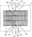
Fig. 1 is the SAW Filter Structures figure by the present invention the 1st embodiment;
As shown in Figure 1, on monocrystalline piezoelectric substrate 11, be formed with the electrode pattern of bar knot shape periodic structure, can encourage SAW.And on this monocrystalline piezoelectric substrate 11, use IDT electrode 12a and reflector electrode 12b, 12c to constitute energy level type 1SAW resonator.And on Piezoelectric Substrates 11, with IDT electrode 13a and reflector electrode 13b, 13c constitutes the 2SAW resonator, and the position of these two resonators is located adjacent one another, forms the acoustics coupling betwixt, constitutes the SAW filter.
Main difference between the SAW of the present invention the 1st embodiment shown in Figure 1 and the electrode pattern structure of conventional SAW shown in Figure 24 is, two of routine shown in Figure 24 each other the adjacent resonator in position public bus electrode 244 IDT electrode part electricity be separated into by the 1st among the present invention the 1st embodiment by bus 14 and the 2nd in bus 15.The 1st bus 14 belongs to the 1SAW resonator and the 2nd bus 15 belongs to the 2SAW resonator.With this bus separate structure, the 1st and the 2SAW resonator can have and fully independently input or output level on electric.That is, the defeated level of the balance of 1SAW resonator is made of the 1st bus electrode 14 and the finger electrode that the IDT electrode 14a that comprises the finger electrode that is coupled with described finger electrode connects and composes.By identical mode, the balance output stage of 2SAW resonator constitutes with the IDT electrode 13a of the finger electrode that comprises the 2nd bus electrode 15 and connect and compose with the finger-like of described finger electrode coupling.Here, 1IDT electrode of the present invention is equivalent to IDT electrode 12a.2IDT electrode of the present invention is equivalent to IDT electrode 13a.
Connect holding wire, can constitute above-mentioned balancing circuitry, add input signal to the 1st bus electrode 14 coupled to each other that is arranged at IDT electrode outside and the point between the 3rd bus electrode 14a, take out output signal from being arranged at IDT electrode outside the 2nd bus electrode 15 coupled to each other and the point between the 4th bus electrode 15a.Use this step, can reach input and the purpose of exporting balance.Find that from end scheme during with above connection, the insertion waste is 32dB.
With regard to an end of above-mentioned balanced type input, line is a bit drawn by the 1st bus electrode 14, and guides to the end in the defeated end of balanced type, and the situation of a bit drawing of line by the 2nd bus electrode 15 has been described.In contrast, 2 situations of drawing line from the 1st and the 2nd bus electrode 14,15 will be described below.
Should insert loss, draw two lines from 2 of the 1st bus electrode 14 and (promptly draw finger electrode 16a, 16b), constitute the end on defeated limit, draw two lines from 2 of the 2nd bus electrode 15 and (promptly draw finger electrode 17a, 17b), constitute the end on defeated limit, can improve the balanced degree in the balanced type input and output side, the loss difference that forms in every end is reduced, be reduced to 2.8dB by above-mentioned big insertion loss.This makes it have the littler loss and the degree of balance to play important effect in the input of balanced type and defeated end in weight is the small portable communication device of important parameter.In other words, among Fig. 1, at IDT electrode 12a and reflector electrode 12b, the space between the 12c forms the finger electrode 16a that outwards draws from the two ends of the 1st bus electrode 14, and 16b as shown in the figure, connects the end of these finger electrodes, obtains above-mentioned effect.The 2nd bus electrode 15 two ends draw finger electrode 17a, 17b also has identical effect.Think and draw finger electrode 16a that 16b is made of the short extraction electrode of length that other electrode that the both ends with the 1st bus electrode 14 are connected has the finger electrode of equal length to be connected with front end with these two finger electrodes.Extraction electrode 17a, the explanation of 17b is identical.
Fig. 2 is the Change Example of the present invention the 1st embodiment shown in Figure 1, and the parts that indicate with same tag among Fig. 1 are identical, and this place saves the explanation to them.
Drawing formation connecting wiring Figure 21 between finger electrode 16a and the 16b on the Piezoelectric Substrates 11, its live width is wider than the resonator electrode width.A part that further specifies also is shown among Fig. 2 constitutes a line 21a who connects usefulness between balanced type input and output side and the outside Wiring member 25a.
Form on the Piezoelectric Substrates 11 and draw connecting wiring Figure 22 between finger electrode 17a and the 17b, its live width is wider than the resonator electrode width.Shown in same figure, the part that will further specify also constitutes the bonding pad 22a that is connected usefulness between balanced type output and the outside wiring member 26a.
14a is protruding for the bus electrode, constitutes another bonding pad 23 that connects usefulness between balanced type output and the outside wiring member 25b.Bus electrode 15b is also protruding, constitutes another bonding pad 24 that is connected usefulness between balanced type output and the outside wiring member 26b.
Said structure can guarantee to have the low insertion loss characteristic of SAW filter of low insertion loss and balanced type input and output side and the good degree of balance effectively, and makes filter characteristic stable.
The example of the SAW filter of single step arrangement has been described in conjunction with Fig. 1 and 2 above.This SAW filter can be used in the multilevel hierarchy.
Fig. 3 is an example, when a plurality of SAW filters on same Piezoelectric Substrates 31 connect and compose multistage connection SAW filter, can improve the characteristic in stopband and the transition band greatly, has some increases although insert loss.The filter that two stage vertical shown in Figure 3 connects comprises IDT electrode 12a shown in Figure 1 and reflector electrode 12b, the 1SAW resonator that 12c constitutes, with usefulness IDT electrode 13a and reflector electrode 13b, the 2SAW resonator that 13c constitutes, these two resonator positions are adjacent, on Piezoelectric Substrates 31, constitute SAW filter 32 and have 33, two parts of its isostructural SAW filter to connect with linking.
Among Fig. 3, extraction electrode 17a on the output limit of the 1st grade of SAW filter 32 and 17b link extraction electrode 16a and the 16b on the input limit of next stage SAW filter 33 respectively with line 39a and 39b.The bus electrode 15a of IDT electrode that is another output of the 1st grade of output links the IDT electrode of another output of next stage with linking 40.
By this mode, even between filter, in the part of 39a and the 29b two connection ID T of place electrodes, the insertion loss in the time of also reducing multistage operating increases, and improves the balanced degree of balanced type input and output side.
The wiring of multiple filter connects same as shown in Figure 1ly on the input and output shown in Figure 3 limit, and same effect and effect is arranged.
Fig. 4 is an example realizing inter-stage and input and output wiring with the wiring diagram that forms on the substrate 41.
On the Piezoelectric Substrates 41, constitute and Fig. 1, the SAW filter has the 1SAW filter 42 and the 2SAW filter 43 of same structure shown in 2 and 3.
Extraction electrode 17a on the output limit of 1SAW filter 42 and 17b are with the extraction electrode 16a and the 16b inter-stage connection electrode 44a that form on the input limit that the 1st inter-stage connection electrode 44a, 44b link 2SAW filter 43, and the width of 44b is wideer than the width of the resonator electrode that forms on the piezoelectricity substrate 41.And, connecting another output 15a of the 1st filter and another input 14a of the 2nd filter 43 with constituting the 2nd inter-stage connection electrode 45, the width of the 2nd inter-stage connection electrode 45 is wideer than the width of the resonator electrode of piezoelectricity substrate 41.
Connect extraction electrode 16a and 1 6b on the input limit of the 1st filter 42 than wide wiring Figure 46 of width of the resonator electrode that forms on the piezoelectricity substrate 41 with its width.And the part expansion of the Figure 48 that connects up constitutes a bonding pad 46a of the outer wiring member of importing with balanced type 47, and the bus electrode 14a of outside IDT electrode outwards enlarges, the bonding pad 48a of the outside wiring member 47b of formation and balanced type input.
On the other hand, connect extraction electrode 17a on the 2nd filter output limit and the zone between the 17b with wiring diagram 46b, the live width of wiring diagram 46b is wideer than the width of the resonator electrode that forms on the piezoelectricity substrate 41.And the part of described wiring figure also prolongs.The bonding pad 46c of the outside wiring diagram 47c of formation and balanced type output, bus electrode 15a extend outwards, the bonding pad 48a of the outside wiring member 47d of formation and balanced type output.
Use this graphic structure, can provide balanced type multistage SAW filter with low insertion loss and excellent balance degree.
Be arranged at inter-stage connection electrode 44b shown in Figure 3, the outside wiring 44c on 45,45a is useful in the external circuit elements of the adjusting usefulness of filter characteristic connects.
And, because the input and output impedance in multistage does not match, therefore the good very situation of transmission characteristic can appear obtaining.
In this case, can be used as matching element such as the reactance component of inductance and be connected to the inter-stage connection electrode in order to regulate.For this reason, the join domain 44c of outside wiring usefulness, 45a is useful.In addition, adopt this structure,, and be connected to the inter-stage connection electrode, therefore, do not need additional space promptly at the reactance component that forms on the same Piezoelectric Substrates or on the substrate that separates as the spirality inductance.Thereby, can easily reduce the filter circuit size.Regulate the reactance component of usefulness and can link inter-stage bonding pad 44c, arbitrary district of 45a, and another district's ground connection.According to experiment, when many reactance components were connected to the 1st bonding pad 44c, the property that can observe the filter transmission characteristic was improved.
(embodiment 2)
Fig. 5 is the SAW Filter Structures figure by the present invention the 2nd embodiment.
Be formed with the electrode pattern of the linear periodic structure of bar on the Piezoelectric Substrates 51 shown in Figure 5, can encourage SAW.Form by IDT electrode 52a and reflector electrode 52b the energy level type 1SAW resonator that 52c constitutes on the Piezoelectric Substrates 51.And, also on Piezoelectric Substrates 51, constitute by IDT electrode and reflector electrode 54b the 3SAW resonator that 54c constitutes.
Here to particularly point out.Have reflector electrode 53b, the IDT electrod assembly of the 2SAW resonator that forms between the 1SAW resonator of 53c and the 3SAW resonator has the structure identical with reflector electrode, and with its length and the 1st and the 3SAW resonator in IDT electrode 51a, the capable 53a of the periodic structure bar line electrode that the finger electrode width of 54a is identical constitutes.
In other words, though the electrod assembly structure of 2SAW resonator and above-mentioned IDT electrode 52a, the structure difference of 54a, and become the periodically capable 53a of bar line electrode, if the electrode cycle is identical, SAW also can send by identical mode.And the acoustic wave character of core 2SAW resonator is different with the acoustic wave character that IDT electrode structure situation produces.
The position is close each other for above-mentioned three SAW resonators, and acoustical coupling is arranged.The electric independence of bus electrode of adjacent component.Be contiguous to the 2SAW of IDT electrode the 1SAW resonator from the two ends of bus electrode 55, outwards the 1st and the 2nd finger electrode 57a that constitutes and 57b constitute the part of balanced type input at IDT electrode 52a and reflector electrode 52b in the space between the 52c.Also be contiguous to the 2SAW of IDT electrode the 3SAW resonator from the two ends of bus electrode 5b, the 3rd and the 4th finger electrode 58a of Gou Chenging and 58b constitute the part of balanced type output at IDT electrode 54a and reflector electrode 54b in the space between the 54c outwardly.Above-mentioned electrode structure is the basic structure by the three-mode SAW filtering of the balanced type input and output side with low insertion loss of the present invention.
Fig. 6 is the connection example of the balanced type input and output side of the present invention used of three-mode SAW filter shown in Figure 5.
As shown in the figure, use line 61a, 61b connects the 1st finger electrode 57a and the 2nd finger electrode 57b of 1SAW resonator, constitutes an input of balanced type input, line 62 is drawn from the bus electrode 55a of outside IDT electrode, constitutes another input of balanced type input.And, use line 63a, 63b connects the 3rd finger electrode 58a and the 4th finger electrode 58b of 3SAW resonator, constitutes an input of balanced type input, draw line 64 from the bus electrode 56a of outside IDT electrode, constitute another output of balanced type input.
Fig. 7 is another embodiment of structure of the balanced type input and output side of three-mode SAW filter.
As shown in the figure, the zone between the 1st finger electrode 57a of 1SAW resonator and the 2nd finger electrode 57b is connected with wiring Figure 71, and the live width of wiring Figure 71 is wideer than the resonator electrode width of formation on the piezoelectricity substrate 51.And figure 71 further extends.Constitute bonding pad 71a with outside wiring member 75a, and, the bus electrode 55a of IDT electrode stretches out, constitute bonding pad 73 with outside wiring member 75, form the 3rd and the 4th finger electrode 58a of 3SAW resonator and the zone between the 58b on the Piezoelectric Substrates 51, constitute resonator electrode, and connect with wiring Figure 72, the live width of wiring Figure 72 is wideer than resonator electrode.Wiring Figure 72 further prolongs, and formation extends outwardly with bonding pad 72a, the bus electrode 56a of IDT electrode of outside wiring member 76a, constitutes the bonding pad 24 with outside wiring member 76.By this structure, identical with the described SAW of the 1st embodiment, might provide described, insert the three-mode SAW filter that loss further reduces and be connected with external circuit easily as the 1st embodiment.
Fig. 8 shows a plurality of three-mode SAW filters that vertical stand stepwise as shown in Figure 5 connects.
As shown in the figure, form the 1st three-mode SAW filter 82 and the 2nd three-mode SAW filter 83 on the Piezoelectric Substrates 81.With connecting line 83a, 83b and 84 with 3 on output limit of the 1st filter 82 and the 4th finger electrode 58a, 58b and the bus electric wire 56a step of output on the limit are connected to the 1st and the 2nd finger electrode 57a on the input limit of the 2nd filter 83, the bus electrode 55a on 57b and the input limit.The run-in index line of input and output circuit and the wire structures of single-section filter shown in Figure 6 are identical.
Fig. 9 is another example of input and output structure of the interstage structure of vertical connection three-mode SAW filter shown in Figure 8.
As shown in the figure, form the 1st three-mode SAW filter 92 and the 2nd three-mode SAW filter 93 on the Piezoelectric Substrates 91.With inter-stage connection electrode 94a, 94b, be connected two filters with 95 inter-stages, inter-stage connection electrode 94a, 94b and 95 width are than with the 3rd and the 4th finger electrode 58a on the output limit that is arranged at the 1st filter 92 on the Piezoelectric Substrates 91,58b, bus electrode 56a, with the 1st and the 2nd finger electrode 57a on the input limit of the 2nd filtering 93 devices, the width of the resonator electrode that the bus electrode 55a on 57b and the input limit constitutes is wide.The regional 94c that forms on the part of each connection electrode, 95a are convenient to be used to regulate filter characteristic with connecting outer member.The input and output circuit layout card of input circuit and output circuit wiring diagram and single-section filter structure shown in Figure 7 is identical.
As mentioned above, press embodiment 1 and 2, because the bus electrode of IDT electrode is independently electric, therefore, can realize the input and output pattern of balance, use electrode grounding, make filter characteristic not influenced by floating capacitance, therefore, can improve the characteristic in stopband and the transition band, and, because feature of the present invention is the extraction electrode structure, thereby can obviously reduce the degree of balance of inserting in loss and the raising balanced type input and output side.
Among the embodiment 3, used the example of a balanced type three-mode filter, wherein the IDT electrode of the core resonator shown in Figure 5 of usefulness has the electrode structure of the periodic structure identical with the reflector electrode structure.Even this part is and the identical IDT electrode structure of electrode structure of usefulness so far to connect and can accurately improve filter characteristic by identical mode with balance wiring of the present invention.
(embodiment 3)
Figure 10 is the structure chart by SAW filter the 3rd embodiment of the present invention.
Among Figure 10, parts 101 are monocrystalline piezoelectric substrates.On Piezoelectric Substrates 101, form electrode pattern, can encourage SAW.Form on the Piezoelectric Substrates 101 with IDT electrode 102a and reflector electrode 102b, the energy level type 1SAW resonator that 102c constitutes also forms with IDT electrode 104a and reflector electrode 104b the 3SAW resonator that 104c constitutes on Piezoelectric Substrates 101.Comprise reflector electrode 103b, the electrode of the 2SAW resonator that forms between the 1SAW resonator of 103c and the 3SAW resonator partly has the structure identical with reflector electrode.
As mentioned above, even the electrod assembly 103a of 2SAW resonator is different with the structure of above-mentioned IDT electrode, and it is capable to become the bar line electrode of periodic structure, if the electrode cycle is identical, SAW also can transmit in identical mode.And, be positioned at the acoustical behavior indifference of acoustic characteristic with the time of the SAW resonator of core with the IDT electrode structure.
And, suppose the 1st and the 3SAW resonator in IDT electrode 102a, the finger electrode width of 104a is W1, the bar line length that constitutes the IDT electrod assembly 103a of 2SAW resonator is W2, and the size relationship of setting between W1 and the W2 is W1≤W2.
The resonator sound coupling that above-mentioned three SAW resonators and another position are contiguous.The finger electrode of IDT electrode 102a in the 1SAW resonator is linked balanced type input " IN ", and the finger electrode of IDT electrode 104a is linked balanced type output " OUT " in the 3SAW resonator.The humorous capable 103a ground connection of bar line electrode of 2SAW along middle periodic structure.
Below explanation has the work of the SAW filter of said structure.
Figure 11 is the incentive mode scatter chart of the SAW filter of present embodiment.Identical with the parts that the same tag indication is arranged among Figure 10.Figure 11 (a) is the electrode structural chart of SAW filter shown in Figure 10.Because the 1st is close to the position of 3SAW resonator, produce the sound coupling betwixt, and motivate the the 1st, the 2 and the 3rd pattern of current potential shown in Figure 11 (b).Here and since be positioned at the center the 3SAW resonator electrod assembly 103a all electrical ground, the polarity of the 2nd pattern Potential distribution is opposite at the center, so, can obtain soaking intensity at the level identical with the 1st and the 3rd pattern.When making the 1st grade of formation, can obtain the wide frequency bandwidth and the rapid SAW filter of attenuation characteristic by the multilevel mode filter that effectively utilizes three incentive modes to constitute.
When Figure 12 was the W1=W2=W that draws with the waveguide pattern analysis, the resonance frequency of each pattern changed and with the graph of relation between the normalized W value of SAW wavelength X.As shown in figure 12, to certain given W value, the difference on the frequency Δ between the 1st pattern and the 2nd pattern/and the 2nd pattern and the 3rd pattern between the value of difference on the frequency Δ 2 different.That is, see 50 systems, as shown in figure 13, the distance between the peak value that passes through characteristic and three modes of resonance of SAW filter does not wait, shown in curve 131.And even input and output when coupling shown in curve 132, remains with pulsation in the frequency band, filter characteristic degenerates.
Here, the lines length W2 that shows the electrod assembly 103a that constitutes the 2nd SAW resonator among Figure 14 with the 1st and the 3SAW resonator in the influence of ratio of the horizontal poor width W 1 of finger electrode of IDT electrode 102a.Among Figure 14, show the normalized value and relation curve of the actual test value of mode of resonance intermediate frequency rate variance (Δ 1 among Figure 13 and Δ 2) with W2/W1 in the SAW filter of the present invention of structure shown in Figure 10.Figure 14 shows be the 1st and the horizontal poor width W 1 of IDT finger electrode of 3SAW resonator when being 6.5 wavelength and combinational gap length be the variation of the long W2 of lines of the 1 wavelength electrod assembly 103a that constitutes the 2SAW resonator.As shown in figure 14, W2/W1 is about 1.13 o'clock Δs 1 and equates with Δ 2, that is, the distance between three resonance frequencys equates.In allowed band, the size relationship between W1 and the W2 can be set at 1≤W2/W1≤1.3.Particularly consider the dispersiveness in the manufacturing, the value of W1 and W2 can be set at 1≤W2/W1≤1.16.
Figure 15 shows the W1=6.5 wavelength, the W2=7.5 wavelength, and the SAW filter passes through characteristic during W2/W1=1.15.Among Figure 15, observed characteristic in the numeral 151 expressions 50 Europe systems, the characteristic during 152 expression couplings.As can be seen, compare with shown in Figure 13, the pulsation in the passband reduces significantly, provides the excellent characteristic of passing through.
As mentioned above, adjacent by 3, three SAW resonators of embodiment of the invention position, the electrod assembly of center SAW resonator is made of lines, and the periodic structure of bar line is longer than the 1st and the horizontal poor width of the IDT finger electrode of 3SAW resonator, all lines ground connection slightly.Use this structure, can obtain to have wide frequency bandwidth, the smooth SAW filter that passes through characteristic and rapid attenuation characteristic.
And, because the bus electricity of IDT electrode centers part is isolated, therefore, might make the IDT electrode wiring of SAW resonator 104a of the IDT electrode 102a of 1SAW resonator and 3SAW resonator all independent, thus the balance input and output of making the SAW filter.As a result, filter characteristic be not subjected to floating capacitance or with the influence of electrode grounding state, further improve the characteristic of stopband and transition band.In addition, the balanced type element such as IC might be connected to the prime and the back level of filtering, and need not with as the spy claimed-and any extra external circuit of dissymmetrical transducer, the noise characteristic of entire circuit is improved.
Among Figure 10, the electrode pattern ground connection that exists in the space of electrod assembly 103a between the IDT of 3SAW resonator electrode 104a and reflector electrode 104c of 2SAW resonator, but structure is not limited thereto; Also can be through the reflector electrode 103b on the electrod assembly 103a both sides, 103c ground connection.
Among this embodiment 3, be that example is illustrated with the SAW filter of single step arrangement.But, as shown in figure 16, with the vertical a plurality of SAW filters 162 that connect on the same Piezoelectric Substrates 161,163, when constituting multistage connecting-type SAW filter, to a certain degree increase is arranged although insert loss, but can significantly improve the characteristic of stopband and transition band, more excellent filter characteristic is provided.In this case, preferably make the 1SAW resonator electrode of prime SAW filter be connected to the balanced type input, the 3SAW resonator electrode of back level SAW resonator is connected to the balanced type output.Here because filter can easily be connected to peripheral circuit such as balanced type front end IC, and need not guarantee to connect up ground connection, therefore, can obtain the littler stable filter characteristic of floating capacitance influence.
And, owing to the input and output impedance at different levels does not match, so, the transmission characteristic that the SAW filter that simple vertical connects does not have.In this case, the reactance component such as inductance can be connected to inter-stage connection electrode Figure 164,165 as matching element.In this case, for making balanced type input and output circuit in full accord, require between electrode Figure 164 and 165, to connect matching element.But, in fact interstage section not with being electrically connected of input and output side, have only the acoustics coupling.And if the direct ground connection of an electrode figure (for example, electrode Figure 165), another electrode figure (for example, electrode Figure 164) is through reactance component ground connection, can realize with two electrode patterns be connected with reactance component the time identical work.And, when adopting this structure, can on electrode pattern, make the ground connection wiring, thereby can reduce line.
(embodiment 4)
Figure 17 is the structure chart by SAW filter the 4th embodiment of the present invention.
Among Figure 17, parts 171 are monocrystalline piezoelectric substrates.On Piezoelectric Substrates 171, form electrode pattern, can the mode identical encourage SAW with the 3rd embodiment.Form with IDT electrode 172a and reflector electrode 172b the energy level type 1SAW resonator that 172c constitutes on the Piezoelectric Substrates 171.On Piezoelectric Substrates 171, also form with IDT electrode 173a and reflector electrode 173b the energy level type 2SAW resonator that 173c constitutes and with IDT electrode 174a and reflector electrode 174b, the energy level type 3SAW resonator of 174c formation.And the position of these three SAW resonators is adjoining, mutually the electric independence of bus electrode of contiguous IDT electrode.And connect reflector electrode with public its bus.The finger electrode of IDT electrode 172a in the 1SAW resonator is connected to balanced type input " IN ", and the finger electrode of IDT electrode 174a is connected to balanced type output " 0UT " in the 3SAW resonator.The whole ground connection of finger electrode of IDT electrode 173a in the 2SAW resonator.And, suppose the 1st and the 3SAW resonator in the horizontal poor width of finger electrode of IDT electrode 172a and 174a when being W1, when the horizontal poor width of the finger electrode of IDT electrode 173a was W2 in the 2SAW resonator, the size relationship of setting W1 and W2 was W1≤W2.
With regard to SAW filter with said structure, the capable IDT electrode 173a that becomes of the bar line electrode of the periodic structure of the electrode structure of the 2SAW resonator of core from above-mentioned the 3rd embodiment, but when accurately carrying out the SAW transmission by model identical, its groundwork is identical with the situation of the 3rd embodiment shown in 10 figure.And, can make by the mode identical with the 3rd embodiment the SAW filter to pass through characteristic smooth and suppress spurious signal in the stopband.
By this embodiment 4, the position of three SAW resonators is adjacent one another are, whole IDT electrode 173 ground connection of formation center 2SAW resonator, their horizontal sentence width is longer than the 1st and the transverse width of the IDT finger electrode of 3SAW resonator slightly, can obtain wide frequency bandwidth and the smooth characteristic and the rapid SAW filter of attenuation characteristic of passing through thus.And, because the bus electricity of IDT electrode centers part is isolated, just might make the IDT electrode 172a of 1SAW resonator and the whole separate cablings of SAW resonator 174a of 2SAW resonator.Therefore, can realize the balance input and output of SAW filter.As a result, filter characteristic is not subjected to the influence of floating capacitance or electrode grounding state.Can improve the characteristic of stopband and transition band.In addition, the balanced type element such as IC can be connected to the prime and the back level of filter, and need not therefore, improve the noise characteristic of entire circuit such as the extra external circuit of balanced-unbalanced transformer.
And, among the embodiment 4, when vertically connecting the multistage connection SAW worry of a plurality of SAW filters formations ripple device, can obviously improve the characteristic of transition band and stopband.It is identical that vertical connection method and reactance component (matching element) are connected to the method and the method among the 3rd embodiment shown in Figure 180 of inter-stage parts, and also identical with the described influence of the 3rd embodiment to the influence of filter characteristic.
Among above-mentioned the 3rd embodiment, as shown in figure 10, the IDT electrode 102a of 1SAW resonator and the IDT electrode 104a of 2SAW resonator are set by the reciprocal mode of phase place.But invention is not limited to this structure, and electrode also can be by the same phase setting.Even in this case, what just additional frequency bands was looked genuine exists pattern slightly different, and effect and effect indifference.Thus, be applied to the 4th embodiment equally.
Among the above-mentioned the 3rd and the 4th embodiment, input and defeated end are balanced types, and still, they are not limited to described structure, and this can ground connection, the monolateral unbalanced type of using respectively of each of input and output side.And, during the ground connection of any one side, can constitute the SAW filter of steady end-unbalanced end.
(embodiment 5)
Figure 18 is the structure chart by SAW filter embodiment 5 of the present invention.
Among Figure 18, parts 181 are monocrystalline piezoelectric substrates.On Piezoelectric Substrates 181, form the electrode pattern of periodic structure, can encourage SAW.Form with IDT electrode 182a and reflector electrode 182b the energy level type 1SAW resonator that 182c constitutes on the Piezoelectric Substrates 181.Also on Piezoelectric Substrates 181, form by IDT electrode 183a and reflector electrode 183b the energy level type 2SAW resonator that 183c constitutes.
As shown in figure 18, connect 3 group the 1st, the 2nd and the 3rd spaced electrode 184a, 184b fall 184c and constituted the IDT electrode 183a that the 2SAW resonator is used.Here, IDT electrode 184a and the 184b that opened in the 1st and the 2nd minute is set, IDT electrode 184b and the 184c that opened in the 2nd and the 3rd minute is set by same phase by opposite phases.The back will illustrate same phase and opposite phase.
The method of attachment of these electrode groups is described as follows.
The IDT electrode 184a that opened in the 1st minute and bottom electrode (outer edges generating line electrode) 1841.Interconnect with the 5th finger electrode 184a5 that comprises among the IDT electrode 184a of top electrode (the inside bus electrode) 1842i of the IDT electrode 184b that opened in the 2nd minute and short connection electrode 184a6 through opening in the 1st minute.And, connect the bottom electrode (outer edges generating line electrode) 1842 of the IDT electrode 184b that opened in the 2nd minute.Bottom electrode (outer edges generating line electrode) 18430 with the ID utmost point 184c that opened in the 3rd minute.
Constituted the IDT electrode 183a that the humorous device of 2SAW is used with said method.
Above-mentioned group technology is that the cutting state by the cutting state of the inside bus electrode and outer edges generating line electrode carries out.
That is,, be divided into IDT electrode 184c that opened in the 3rd minute and the IDT electrode 184b that opened in the 2nd minute owing to cut apart top electrode 1843i and top electrode 1842i.And, owing to cut apart bottom electrode 1842o and bottom electrode 1841o, be divided into IDT electrode 184b that opened in the 2nd minute and the IDT electrode 184a that opened in the 1st minute.
And the 1st is adjacent with the 2 two resonator position, but and two resonators constitute between the sound coupling.
And, the top electrode of IDT electrode 182a and bottom electrode are connected respectively to balanced type input " IN ", the top electrode of the IDT electrode 184b that constitutes IDT electrode 184a craftsman's bottom electrode of opening in the 1st minute of IDT electrode 183a and opened in the 2nd minute is linked a balanced type output " OUT ", the bottom electrode of the bottom electrode of the IDT electrode 184b that opened in the 2nd minute and the electrode 184c that opened in the 3rd minute is connected to another balanced type output " OUT ", the top electrode ground connection of the top electrode of the IDT electrode 184a that opened in the 1st minute and the IDT electrode 184c that opened in the 3rd minute, thus, constitute the balanced type input and output.
Here, same phase and opposite phase have been carried out above explanation.
The positional structure relation of adjacent two finger electrodes (a pair of finger electrode) at first, has been described.
Be meant that by two adjacent finger electrodes of same phase relation one of described two finger electrodes are connected to the inside bus electrode and extend from inside to outside, another finger electrode is linked outer edges generating line electrode and extension outside in, a kind of like this annexation.And be meant that by adjacent two finger electrodes of opposite phase relation described two finger electrodes all are connected to the inside bus electrode and extension from inside to outside, or two finger electrodes all are connected to outer edges generating line electrode and extend such annexation from outside to inside.Here, the inside is different with the electric charge of outer edges generating line electrode, and the pitch between described adjacent two finger electrodes (two center between distance) is 1/2 λ, and wherein λ is the wavelength of the surface acoustic wave of excitation.If the pitch between the finger electrode can be (m+1/2) λ, m=0,1,2,3 ...In this case, if pitch is (m+1) λ, enlightening just expression concerns fully opposite with above-mentioned to phase relation and antiphase.
In fact, when observing the IDT electrode 184a that opened in the 1st minute shown in Figure 180, for example, the 1st finger electrode 184a1 and the 2nd finger electrode 184a2 are that same-phase relation, the 4th finger electrode 184a4 and the 5th finger electrode 184a5 also are the same-phase relations, and the whole finger-like electricity that comprise among the IDT electrode 184a that opened in the 1st minute are the same-phase relation mutually.Equally, the whole finger electrodes that comprise among IDT electrode 184b, the 184c that opened in the 2nd and the 3rd minute are same-phase relations.
Afterwards, about a pair of finger electrode 184a5 and 184b1, because finger electrode 184a5 links outer edges generating line electrode 1841o, finger electrode 184b1 is connected to outer edges generating line electrode 1842o, and they are antiphase relations.IDT electrode 184a that these two adjacent electrodes were opened at the 1st minute and the separated point place between the 2IDT electrode 184b.
And much less, the antiphase of the above-mentioned position relation of three groups of electrodes or same-phase are the relations according to above-mentioned adjacent two finger electrodes.This point is also identical in other embodiments.
And, the width of the short length direction of the 5th finger electrode 184a5 below will be described.
Among Figure 18, the width of the 5th finger electrode 184a5 in the structure with shown in the width of other finger electrode identical.But, be not limited to this.Its width can certainly be wideer than the width of other finger electrode.The resistance value of finger electrode is reduced.And, comprise that the resistance of its IDT electrode has also diminished, can subtract the insertion loss thus.This also can be applicable to other embodiment.
As follows about above-mentioned job description of pressing the SAW filter that the 5th embodiment constitutes.
Figure 19 is the capacitor equivalent circuit diagram by the 5th embodiment, C1 is the capacitance that constitutes the IDT electrode 182a of 1SAW resonator among the figure, Ca, Cb and Co are the 1st, the 2nd and 3IDT electrode 184a, and the capacitance of 184b and 184c, Ca, Cb and Cc contain the total capacitance C2 that becomes 2AW resonator IDT electrode 183a.Here, suppose that the finger electrode coupling numbers that comprises among the IDT electrode 183a is n, the IDT electrode 184a that the the 1st, the 2nd and the 3rd minute opens, the coupling numbers of 184b, 184c are respectively n
a, n
b, n
c, its pass is n=n
a+ n
b+ n
cIDT electrode 182a in the above-mentioned SAW filter, the capacitance of 183a is by the coupling numbers decision of electrode.The coupling numbers of supposing IDT electrode 182a is n, and the electrode capacity of IDT finger electrode coupling is C, C
1, C
a, C
dAnd C
cCan be shown in down respectively:
C
1=n×c
C
a=n
a×C=C
1×n
a/n=C
1×n
a/(n
a+n
b+n
c)
C
b=n
b×C=C
1×n
b/n=C
1×n
b/(n
a+n
b+n
c)
C
c=n
c* C=C
1* n
c/ n=C
1* n
c/ (n
a+ n
b+ n
c) and, from the capacitor equivalent circuit diagram of Figure 19, total capacitance C2 can be represented with following formula 1 with Ca, Cb, Cc: formula 1:
For example, suppose IDT electrode 184a separately, the coupling numbers of 184b and 184c is equal, that is: n
a=n
b+ n
c=n/3, then relation becomes C
2=C
1* 1/2, C
2Capacity become half of C1 capacity.Change IDT electrode 184a separately, the coupling numbers n of 184b and 184c
a, n
bAnd n
cTotal capacitance excursion by equation (1) IDT electrode 183a is C
1* 1/4<C
2<C
1That is, use the total capacitance of recently controlling IDT electrode 183a of cutting apart of IDT electrode 184a, 184b separately and 184c.
And under this situation, the electric charge on the electrode of IDT electrode 184,184b and the 184c that held in the the 1st, the 2nd and the 3rd minute can not cancelled out each other.By the IDT electrode 184a that opened in the the 1st, the 2nd and the 3rd minute, it is identical that the SAW that 184b and 184c constitute becomes phase place.So 2SAW resonator and 1SAW resonator have same resonance characteristic.And, make the 1st adjacently with the position of 2SAW resonator, their system is identical routinely modes are as laterally die combination resonance filter work.
As mentioned above, by embodiment 5, SAW filter with balanced type input and output is in the additional frequency bands selectivity and have and excellent specific property is arranged aspect the narrow frequency bandwidth, and, with by of the present invention be the electrode structure of the IDT electrode that constitutes of feature with the IDT electrode that separates, can control the output impedance of SAW filter.
Among the 5th embodiment, with the ID utmost point 183a that constitutes the 2SAW resonator is that the basis is illustrated, constitute the relevant the 1st of IDT electrode 183a, the electrode 184a that opened in the 2nd and the 3rd minute, 184b and 184c are provided with by the mode with left-to-right, so that describe, but placement is not limited to said sequence in proper order, can place 184a, 184b and 184c from right to left.The electrode pattern of IDT electrode 183a can turn upside down.In this case, as shown in figure 20, connect the IDT electrode 204a that opened in 3 group the 1st, the 2nd and the 3rd minute, 204b and 204c are formed in the IDT electrode 203a that constitutes the 2SAW resonator on the Piezoelectric Substrates 201.IDT electrode 204a and the 204b that opened in the 1st and the 2nd minute is set by reverse mode, IDT electrode 204b and the 204c that opened in the 2nd and the 3rd minute is set by same phase, connect the top electrode of the IDT electrode 204a that opened in the 1st minute and the bottom electrode of the IDT electrode 204b that the 2nd minute opens, connect the top electrode of the IDT electrode 204b that opened in the 2nd minute and the top electrode of the ID utmost point 204c that the 3rd minute opens, constitute IDT electrode 203a, IDT electrode 203a constitutes the 2SAW resonator.Among Figure 20, it is to place 204a, 204b and 204c from a left side in proper order that the IDT utmost point 204a that separates, 204b and 204c try to gain placement, but also can place from the right side.Under these situations, just the placement order of IDT electrode is different in the electrode structure, but the performance of SAW filter is identical with institute's obtained performance among Figure 18.
Among the embodiment 5, the coupling numbers of IDT electrode 182a and the IDT electrode 184a that opened in the the 1st, the 2 and the 3rd minute, the coupling sum of 184b and 184c equate respectively.But they need not make coupling numbers accurately identical, can set the IDT electrode 184a that opened in the the 1st, the 2 and the 3rd minute arbitrarily, the ratio of the coupling numbers of 184b and 184c.And set IDT electrode 183c to cut apart number be 3, appoint that to cut apart number also can be that other are several.And, although the electricity end of IDT electrode 182a is to be example with the balanced type,, but any the equal ground connection and constitute jiggly electricity end in the upper/lower electrode.In this case, can constitute the SAW filter of balanced-unbalanced end.In the structure that has adopted, reflector electrode 182b and 183b, 182c and 183c are that electricity separates.But two parts can connect, and ground connection.And, for constituting the 2SAW resonator, although be designed to IDT electrode 184a separately, 184b and 184c constitute IDT electrode 183a, but it also can constitute the 1SAW resonator, in this case, the 1st and the 2SAW resonator all can control the impedance on input and output limit.
(embodiment 6)
Figure 21 is the structure chart of electrode pattern of the SAW filter of the embodiment of the invention 6.
Among Figure 21, parts 211 are monocrystalline piezoelectric substrates, form the lines of the periodic structure of electroplax figure on described Piezoelectric Substrates 211, can encourage SAW.Form the energy level type 1SAW resonator that constitutes with IDT electrode 212a and reflector electrode 212b, 212c on the Piezoelectric Substrates 211.And, on Piezoelectric Substrates 211, form with IDT electrode resonator.And, on Piezoelectric Substrates 211, form with IDT electrode 213a and reflector electrode 213b the energy level type 2SAW resonator that 213c constitutes.
The IDT electrode 213a that constitutes the 2SAW resonator constitutes with 3 group the 1st, the 2 and the 3rd minute IDT electrode 214a, 214b that opens of connection and 214c.1st, the IDT electrode 214a that opened in the 2nd and the 3rd minute, 214b and 214c are all by the same phase setting, the top electrode of the IDT electrode that connects the top electrode of the IDT electrode 214a that opened in the 1st minute and opened in the 2nd minute, and connect the following electricity of the IDT electrode 214b that opened in the 2nd minute and the bottom electrode of the IDT electricity 214c that opened in the 3rd minute, form the IDT electrode 213a that constitutes the 2SAW resonator.And make the 1st adjacently with the position of 2SAW resonator, and and produce the acoustics coupling betwixt, constitute the SAW filter.
And the upper/lower electrode of IDT electrode 212a is linked balance leveling style input " IN " respectively.The top electrode that constitutes the top electrode of the IDT electrode 214a that opened in the 1st minute of IDT electrode 213a and the IDT electrode 214b that the 2nd minute opens is connected to one side " OUT " of balanced type output, and the bottom electrode of the bottom electrode of the IDT electrode 214b that opened in the 2nd minute and the IDT electrode 214c that opened in the 3rd minute is connected to the another side " OUT " of balanced type output.The bottom electrode ground connection of the electrode of the IDT electrode 214a that opened in the 1st minute and the IDT electrode 214c that opened in the 3rd minute constitutes the balanced type input and output side.
In the SAW filter of above-mentioned formation, the 1SAW resonator has identical structure with the 1SAW resonator of the 5th embodiment, and 2SAW resonator and the difference of the 2SAW resonator of the 5th embodiment only are that the method for attachment of electrode pattern and the former IDT electrode 213a and the latter's the method for attachment of IDT 183a is different.Even in this case, the IDT electrode 214a that separates, the electric charge on 214b and the 214c is not cancelled out each other yet, but by the IDT electrode 214a that separates, 214b, the SAW phase place that constitutes with 214c is identical, and the 2SAW resonator has identical resonance characteristic with the 1SAW resonator.Therefore, be provided with the 1st and the 2SAW resonator, the SAW filter of this embodiment 6 is with the horizontal die combination resonator type filter work of the mode identical with embodiment 5 as routine close to each otherly.And the SAW filter with leveling style input and output has the excellent specific property of additional frequency bands selectivity and narrow-band, and can control the input and output impedance of SAW filter, therefore, provides the identical effect of SAW filter of the 5th embodiment.
Among the 6th embodiment, it is 214a that the IDT electrode 214a that separates, 214b and 214c are designed to from the left side, 214b and 214c, but also can be this order from the right.And, IDT electrode 213a to cut apart number be 3, also can be other any number.The electricity end of IDT electrode 212a is example with the balanced type, but also can be changed into unbalanced electricity end, can use any electrode grounding in electrode or the bottom electrode.In this case, can constitute the SAW filter of balanced-unbalanced electricity end.Although structure is reflector electrode 212b and 213b, 212c and 213c are that electricity separates, and two parts also can connect and ground connection.And although determine by the IDT electrode 214a that separates, the IDT electrode 213a that 214b and 214c constitute constitutes the 2SAW resonator, and this also can constitute the 1SAW resonator, or constitutes the 1st and the 2 two resonator.Under the situation of back, can constitute the controlled SAW filter of input and output impedance.
(embodiment 7)
Among the embodiment 5 and 6, be that example is described with SAW filter with single step arrangement.But this SAW filter also can be used in the multilevel hierarchy.
Figure 22 is the example of electrode pattern structure by the multilevel hierarchy of the SAW filter of the embodiment of the invention 7.Among Figure 22, parts 221 are monocrystalline piezoelectric substrates.The vertical a plurality of SAW filters that connect on the Piezoelectric Substrates when constituting multistage connections SAW filter, can significantly improve the characteristic of stopband and transition band, although some increase of order appearance insertion loss.
Two stage vertical among Figure 22 connects filter and comprises 1SAW filter and 2SAW filter, the 1SAW filter comprises with IDT electrode 222a and reflector electrode 22b, the 1SAW resonator that 222c constitutes and with IDT electrode 223a and reflector electrode 223b, the 2SAW resonator that 223c constitutes, two SAW resonator positions are adjacent, the 2SAW filter comprises the 3SAW resonator that constitutes with IDT electrode 224a and reflector electrode 224b and 224c and with IDT electrode 225a and reflector electrode 225b, the 4SAW resonator that 225c constitutes, they are provided with adjacent to each other, on formation and the Piezoelectric Substrates 221.The IDT electrode 225a that constitutes the 4SAW resonator in the 2SAW filter is with connecting the IDT electrode 226a that opened in 3 group the 1st, the 2nd and the 3rd minute, and 226b and 226c constitute.By opposite phase IDT electrode 226a that opened in the 1st minute and the IDT electrode 226b that opened in the 2nd minute are set, IDT electrode 226b that opened in the 2nd minute and the IDT electrode 226c that opened in the 3rd minute are set by same phase.Afterwards, the top electrode interconnection of the bottom electrode of the IDT electrode 226a that opened in the 1st minute and the IDT electrode 226b that opened in the 2nd minute, the bottom electrode of the IDT electrode 226b that opened in the 2nd minute is connected with the bottom electrode of the IDT electrode 226c that opened in the 3rd minute, thus, has formed the IDT electrode 225a that constitutes the 4SAW resonator.One of extraction electrode on the 1st grade of SAW filter output limit is connected to the relative extraction electrode on the input limit of relative next stage SAW filter with inter-stage connection electrode Figure 22 7a, another the 1st grade of IDT electrode is connected to the IDT of another subordinate electrode on the input limit with inter-stage connection electrode Figure 22 7b on the output limit, constitutes two-stage SAW filter thus.
And the top electrode and the bottom electrode that constitute the IDT electrode 222a of 1SAW resonator in the 1SAW filter are connected respectively to balanced type input " IN ".And, constitute among the IDT electrode 225a of the 4SAW resonator in the 2SAW filter, the top electrode of the bottom electrode of the IDT electrode 226a that opened in the 1st minute and the IDT electrode 226b that opened in the 2nd minute is connected to one side OUT of balanced type output, the bottom electrode of the bottom electrode of the IDT electrode 226b that opened in the 2nd minute and the IDT electrode 225c that opened in the 3rd minute is linked the another side OUT of balanced type output, the top electrode ground connection of the top electrode of the IDT electrode 226a that opened in the 1st minute and the IDT electrode 226c that opened in the 3rd minute.Constitute the leveling style input and output side.
But,,, can not obtain the good transmission characteristic of defined with simple vertical a plurality of SAW filters that connect because multistage input and output impedance does not match.In this case, the reactance component such as inductance can be connected to the inter-stage connection electrode to regulate as matching element.Also can adopt a kind of like this structure, that is, and on the same Piezoelectric Substrates 221 or the Piezoelectric Substrates of separating, formation is the reactance component of representative with the spirality inductance, and it is connected to the inter-stage connection electrode, thus, can easily reduce the size of filter, and need not additional space.Regulate the reactance component of usefulness, can be connected to any one among the 1st inter-stage connection electrode Figure 22 7a and the 227b, but and another inter-stage electrode connection layout ground connection.According to experiment, as shown in figure 22, reactance component 228 is connected to inter-stage connection electrode Figure 22 7a, to improve the symmetry of filter transmission characteristic.
Use said structure, there is the SAW filter of balanced type input and output among this embodiment 7 to have the narrow-band characteristic, with inter-stage connection electrode Figure 22 7a, 227b connects two SAW filters, the sharper mirror of additional frequency bands selectivity of additional frequency bands selectivity ratios single-section filter can be made, the output impedance of SAW filter can also be controlled.
Among the 7th embodiment, constitute among the IDT electrode 225a that the 4SAW resonator is used in the 2SAW filter, it is 226a, 226b and 226c that the 1st, the 2nd and the 3rd spaced electrode 226a, the 226b of formation IDT electrode 225a and 226c are arranged to a left side, describe with simplification, but this order also can rise on the right.Can putting upside down up and down of the electrode pattern of IDT electrode 225a.
Among the embodiment 7, the separately number of IDT electrode 225a is 3, but also can be set at other number.The electricity end that with the balanced type is the IDT electrode 222a of example also can make top electrode or bottom electrode ground connection become unbalanced type electricity end.In this case, can constitute the SAW filter of balanced-unbalanced end.IDT electrode 225a can be the IDT electrode 213a among the embodiment 6.Under these situations, IDT electrode 234a has only the electrode structure difference, can obtain the SAW filter characteristic identical with SAW filter characteristic shown in Figure 22, although adopt this structure, reflector electrode 222b and 223b, 222c and 223c are that electricity separates, and two elements can connect and ground connection.And although determine that the IDT electrode 225a that 226b and 226c constitute constitutes the 4SAW resonator with IDT electrode 226a separately, it can constitute the 1SAW resonator, or constitutes the 1st and the 4 two SAW resonator simultaneously.Under the latter event, can control the input and output impedance of SAW filter.And the progression of SAW is two-stage, but progression can be bigger, and at this moment, filter characteristic is sharp-pointed, and the additional frequency bands selectivity is better.
(embodiment 8)
Figure 23 is the SAW filter electrode graphic structure figure by the embodiment of the invention 8.Among Figure 23, parts 231 are monocrystalline piezoelectric substrates.On described Piezoelectric Substrates 231, form electrode pattern, can encourage SAW.Form the energy level type 1SAW resonator that constitutes by IDT electrode 232a and reflector electrode 232b, 232c on the Piezoelectric Substrates 231.And, on Piezoelectric Substrates 231, form with DT electrode 234a and reflector electrode 234b the 3SAW resonator that 234c constitutes.The 1st and the 3SAW resonator between form the reflector electrode 233b that the electrod assembly 233a of 2SAW resonator has, 233c has same structure, as reflector electrode.And, even with the structure of the electrod assembly 223a of 2SAW resonator be not the IDT electrode structure, when but periodically the bar line electrode is capable, if the electrode cycle is identical, SAW can propagate by identical mode, therefore, be in the acoustical behavior of 2SAW resonator of core and the acoustical behavior of IDT electrode structure and do not have difference.
And the IDT electrode 234a that constitutes 3SAW constitutes by connecting IDT electrode 235a, the 235b and the 235c that opened in 3 group the 1st, the 2nd and the 3rd minute.Be provided with the 1st and the 2nd fen by opposite phase and open IDT electrode 235a and 235b; By same phase position the 2nd with opened IDT electrode 235b and 235c on the 3rd minute, the bottom electrode of the IDT electrode 235a that opened in the 1st minute is connected with the top electrode of the IDT electrode 235b that opened in the 2nd minute; The bottom electrode of the IDT electrode 235b that opened in the 2nd minute is connected with the bottom electrode of the IDT electrode 235c that opened in the 3rd minute, forms the IDT electrode 234a that constitutes the 3SAW resonator.
Above-mentioned 3 SAW resonator positions are adjacent one another are, the electric independence of bus electrode of adjacent component.The bottom electrode that constitutes the IDT electrode 232a of the 1SAW resonator in the 1SAW filter is connected respectively to balanced type input " IN ".And, constitute among the IDT electrode 234a of 3SAW resonator.And, constitute among the IDT electrode 234a of 3SAW resonator, the bottom electrode of the IDT electrode 235a that opened in the 1st minute of formation IDT electrode 234a and the top electrode of the IDT electrode 235b that the 2nd minute opens are connected to one side OUT of balanced type output, the bottom electrode of the bottom electrode of the IDT electrode 235b that opened in the 2nd minute and the IDT electrode 235c that opened in the 3rd minute is connected to the another side OUT of balanced type output, the top electrode ground connection of the top electrode of the IDT electrode 235a that opened in the 1st minute and the IDT electrode 235c that opened in the 3rd minute, constitute the balanced type input and output side, the bar line electrode line 233a ground connection of periodic structure in the 2SAW resonator.
As mentioned above, be 3 adjacent SA resonators to be set by the feature of the SAW filter of the embodiment of the invention 8, and make acoustics coupling therebetween, and make it have filter characteristic by the direction parallel with the SAW direction of propagation.
Simultaneously, represent among the open 8-51334 of Japan's special permission by the IDT electrode in the disclosed SAW multi-mode filter of the inventor with the IDT electrode 233a of 2SAW resonator in the formation of the present invention SAW filter, and the openly identical work of the described filter of 8-51334 of described Japan's special permission is arranged.That is, constitute the SAW resonator by 3 grades, filter has wide frequency bandwidth, and additional frequency bands selectivity excellence can be controlled the output impedance of SAW filter.
Among the 8th embodiment, constitute among the IDT electrode 234a of 3SAW resonator, it is 235a, 235b and 235c that the 1st, the 2nd and 3IDT electrode 235a, the 235b of formation IDT electrode 234a and 235c are designed to from left side order, so that describe, but this order also can be from the right.The electrode pattern of IDT electrode 234a also can turn upside down.IDT electrode 234a can be the structure of the IDT electrode 213a shown in the embodiment 6.Under these situations, IDT electrode 234a is the electrode structure difference, but the SAW filter characteristic is same as shown in Figure 23.
And the number of cutting apart of IDT electrode 234a is given as 3, but also can be any other number.Be that the electricity end of the IDT electrode 232a of example also can be used electrode or bottom electrode ground connection becomes unbalanced type electricity end with the balanced type.In this case, can constitute SAW filter with balanced-unbalanced end.Although adopt this structure, reflector electrode 232b and 233b, 232c and 233c are that electricity separates.Two element ground connection.And although regulation constitutes the 3SAW resonator with the IDT electrode 234a that separately IDT electrode 235a, 235b and 235c constitute, it also can constitute the 1SAW resonator, or constitutes the 1st and the 3 two SAW resonator.Under the latter event, the input and output impedance of SAW filter is controlled.
Among this embodiment 8, described IDT electrode 233a through be arranged at its right on IDT electrode 232a and the electrode figure ground connection between the anti-device electrode 232c.But, also can be through being arranged at IDT electrode 233a on its left side and the electrode figure ground connection between the reflector electrode 233c, or change the electrode figure ground connection between any in being arranged at IDT electrode 234a and reflecting electrode 234b or 234c into.Although adopted this structure, that is, reflector electrode 232b and 233b on each SAW resonator, 232c and 233c are that electricity separates, and they can connect respectively and ground connection.And IDT electrode 233a can be through reflector electrode 232b, 232c, 233b, 233c, any electrode among 234b and the 234c and ground connection.The electrode structure of IDT electrode 233a can be identical with the electrode structure of IDT electrode 232a.SAW also propagates state by same way as in this case, and can obtain the filter characteristic identical with this embodiment 8.And although the IDT electrode 234a that separates that constitutes the 3SAW resonator has been described, it also can constitute the 1SAW resonator, or constitutes this two SAW resonators.Under the latter event, the input and output impedance of SAW resonator is controlled.Although the 1st is identical to the 3SAW resonator structure, their structure also can be different.The SAW filter of embodiment 8 can be that two stage vertical connects, and in this case, the additional frequency bands selectivity characteristic can be more sharp-pointed.
Piezoelectric Substrates among the present invention is preferably used the ST sliced crystal with excellent temperature characterisitic, but also available such as LiTaO
3, LiNbO
3, Li
2B
4O
7, La
3Ga
3SiD
14Deng substrate.Electrode material is easy to control with the less aluminium film of density, its thickness, but also can use gold electrode.
And the present invention is not only applicable to above-mentioned SAW resonator.Also be applicable to (be a kind of SAW, or pseudo surface wave) (obstacle wave (Surface Skimming Balk Wave) is removed on the surface to SSBW.