CN115765433A - Chip embedded power converter - Google Patents
Chip embedded power converter Download PDFInfo
- Publication number
- CN115765433A CN115765433A CN202211229113.XA CN202211229113A CN115765433A CN 115765433 A CN115765433 A CN 115765433A CN 202211229113 A CN202211229113 A CN 202211229113A CN 115765433 A CN115765433 A CN 115765433A
- Authority
- CN
- China
- Prior art keywords
- inductor
- converter
- switch
- embedded
- power
- Prior art date
- Legal status (The legal status is an assumption and is not a legal conclusion. Google has not performed a legal analysis and makes no representation as to the accuracy of the status listed.)
- Pending
Links
Images


Classifications
-
- H—ELECTRICITY
- H02—GENERATION; CONVERSION OR DISTRIBUTION OF ELECTRIC POWER
- H02M—APPARATUS FOR CONVERSION BETWEEN AC AND AC, BETWEEN AC AND DC, OR BETWEEN DC AND DC, AND FOR USE WITH MAINS OR SIMILAR POWER SUPPLY SYSTEMS; CONVERSION OF DC OR AC INPUT POWER INTO SURGE OUTPUT POWER; CONTROL OR REGULATION THEREOF
- H02M3/00—Conversion of dc power input into dc power output
- H02M3/02—Conversion of dc power input into dc power output without intermediate conversion into ac
- H02M3/04—Conversion of dc power input into dc power output without intermediate conversion into ac by static converters
- H02M3/10—Conversion of dc power input into dc power output without intermediate conversion into ac by static converters using discharge tubes with control electrode or semiconductor devices with control electrode
- H02M3/145—Conversion of dc power input into dc power output without intermediate conversion into ac by static converters using discharge tubes with control electrode or semiconductor devices with control electrode using devices of a triode or transistor type requiring continuous application of a control signal
- H02M3/155—Conversion of dc power input into dc power output without intermediate conversion into ac by static converters using discharge tubes with control electrode or semiconductor devices with control electrode using devices of a triode or transistor type requiring continuous application of a control signal using semiconductor devices only
- H02M3/156—Conversion of dc power input into dc power output without intermediate conversion into ac by static converters using discharge tubes with control electrode or semiconductor devices with control electrode using devices of a triode or transistor type requiring continuous application of a control signal using semiconductor devices only with automatic control of output voltage or current, e.g. switching regulators
- H02M3/158—Conversion of dc power input into dc power output without intermediate conversion into ac by static converters using discharge tubes with control electrode or semiconductor devices with control electrode using devices of a triode or transistor type requiring continuous application of a control signal using semiconductor devices only with automatic control of output voltage or current, e.g. switching regulators including plural semiconductor devices as final control devices for a single load
-
- G—PHYSICS
- G05—CONTROLLING; REGULATING
- G05F—SYSTEMS FOR REGULATING ELECTRIC OR MAGNETIC VARIABLES
- G05F1/00—Automatic systems in which deviations of an electric quantity from one or more predetermined values are detected at the output of the system and fed back to a device within the system to restore the detected quantity to its predetermined value or values, i.e. retroactive systems
- G05F1/10—Regulating voltage or current
- G05F1/46—Regulating voltage or current wherein the variable actually regulated by the final control device is dc
-
- G—PHYSICS
- G06—COMPUTING; CALCULATING OR COUNTING
- G06F—ELECTRIC DIGITAL DATA PROCESSING
- G06F1/00—Details not covered by groups G06F3/00 - G06F13/00 and G06F21/00
- G06F1/26—Power supply means, e.g. regulation thereof
-
- H—ELECTRICITY
- H02—GENERATION; CONVERSION OR DISTRIBUTION OF ELECTRIC POWER
- H02M—APPARATUS FOR CONVERSION BETWEEN AC AND AC, BETWEEN AC AND DC, OR BETWEEN DC AND DC, AND FOR USE WITH MAINS OR SIMILAR POWER SUPPLY SYSTEMS; CONVERSION OF DC OR AC INPUT POWER INTO SURGE OUTPUT POWER; CONTROL OR REGULATION THEREOF
- H02M3/00—Conversion of dc power input into dc power output
- H02M3/003—Constructional details, e.g. physical layout, assembly, wiring or busbar connections
-
- H—ELECTRICITY
- H02—GENERATION; CONVERSION OR DISTRIBUTION OF ELECTRIC POWER
- H02M—APPARATUS FOR CONVERSION BETWEEN AC AND AC, BETWEEN AC AND DC, OR BETWEEN DC AND DC, AND FOR USE WITH MAINS OR SIMILAR POWER SUPPLY SYSTEMS; CONVERSION OF DC OR AC INPUT POWER INTO SURGE OUTPUT POWER; CONTROL OR REGULATION THEREOF
- H02M3/00—Conversion of dc power input into dc power output
- H02M3/02—Conversion of dc power input into dc power output without intermediate conversion into ac
- H02M3/04—Conversion of dc power input into dc power output without intermediate conversion into ac by static converters
- H02M3/10—Conversion of dc power input into dc power output without intermediate conversion into ac by static converters using discharge tubes with control electrode or semiconductor devices with control electrode
- H02M3/145—Conversion of dc power input into dc power output without intermediate conversion into ac by static converters using discharge tubes with control electrode or semiconductor devices with control electrode using devices of a triode or transistor type requiring continuous application of a control signal
- H02M3/155—Conversion of dc power input into dc power output without intermediate conversion into ac by static converters using discharge tubes with control electrode or semiconductor devices with control electrode using devices of a triode or transistor type requiring continuous application of a control signal using semiconductor devices only
- H02M3/156—Conversion of dc power input into dc power output without intermediate conversion into ac by static converters using discharge tubes with control electrode or semiconductor devices with control electrode using devices of a triode or transistor type requiring continuous application of a control signal using semiconductor devices only with automatic control of output voltage or current, e.g. switching regulators
- H02M3/158—Conversion of dc power input into dc power output without intermediate conversion into ac by static converters using discharge tubes with control electrode or semiconductor devices with control electrode using devices of a triode or transistor type requiring continuous application of a control signal using semiconductor devices only with automatic control of output voltage or current, e.g. switching regulators including plural semiconductor devices as final control devices for a single load
- H02M3/1584—Conversion of dc power input into dc power output without intermediate conversion into ac by static converters using discharge tubes with control electrode or semiconductor devices with control electrode using devices of a triode or transistor type requiring continuous application of a control signal using semiconductor devices only with automatic control of output voltage or current, e.g. switching regulators including plural semiconductor devices as final control devices for a single load with a plurality of power processing stages connected in parallel
-
- Y—GENERAL TAGGING OF NEW TECHNOLOGICAL DEVELOPMENTS; GENERAL TAGGING OF CROSS-SECTIONAL TECHNOLOGIES SPANNING OVER SEVERAL SECTIONS OF THE IPC; TECHNICAL SUBJECTS COVERED BY FORMER USPC CROSS-REFERENCE ART COLLECTIONS [XRACs] AND DIGESTS
- Y02—TECHNOLOGIES OR APPLICATIONS FOR MITIGATION OR ADAPTATION AGAINST CLIMATE CHANGE
- Y02B—CLIMATE CHANGE MITIGATION TECHNOLOGIES RELATED TO BUILDINGS, e.g. HOUSING, HOUSE APPLIANCES OR RELATED END-USER APPLICATIONS
- Y02B70/00—Technologies for an efficient end-user side electric power management and consumption
- Y02B70/10—Technologies improving the efficiency by using switched-mode power supplies [SMPS], i.e. efficient power electronics conversion e.g. power factor correction or reduction of losses in power supplies or efficient standby modes
Abstract
A direct current-to-direct current (DC-DC) converter includes a chip-embedded Integrated Circuit (IC), one or more switches, and an inductor. The IC may be embedded in a printed circuit board. The IC may include a driver, a switch, and a Pulse Width Modulation (PWM) controller. The IC and/or the switch may include edan. Inductors may be stacked over the IC and/or the switch to reduce the overall footprint. One or more capacitors may also be stacked over the IC and/or the switch. The vias may couple the inductors and/or capacitors to the IC (e.g., to the switches). The DC-DC converter can provide better transient performance, have lower ripple, or use fewer capacitors. The parasitic effects that would impede higher effective switching speeds are reduced. The size and overall footprint of the inductor is reduced. A multiple inductor arrangement may improve performance. Various feedback systems may be used, such as a ripple generator in a constant on or off time modulation circuit.
Description
Cross Reference to Related Applications
The application is a divisional application of a Chinese patent application with the application number of 201880016757.6. The chinese patent application with application number 201880016757.6 is a chinese national phase application of international application PCT/US 2018/017109. It claims priority from U.S. patent application No.15/428,019 filed on 8/2/2017 and U.S. patent application No.15/669,838 filed on 4/8/2017. The disclosures of these patent applications are hereby incorporated in their entirety by reference.
Technical Field
The present disclosure relates to electronic systems, direct current-to-direct current (DC-DC) converters, electronic device designs, and electronic device production techniques.
Background
Although a variety of DC-DC converters have been known, these DC-DC converters are constructed from non-ideal components and/or arrangements that present parasitic losses and inefficiencies, and there is a need for improved power converters.
Content of application
Some embodiments of a direct current-to-direct current (DC-DC) power converter are disclosed, the DC-DC power converter comprising: a lower Printed Circuit Board (PCB) portion having a bottom side and a top side; an upper Printed Circuit Board (PCB) portion having a bottom side and a top side; an embedded circuit located between a top side of the lower PCB section and a bottom side of the upper PCB section, the embedded circuit comprising: a pulse width modulator and at least one switch; one or more vias extending through the upper PCB portion; an inductor located over the top side of the upper PCB portion, wherein one or more vias are electrically coupled with the inductor and the embedded circuit. This embodiment may have any combination of the following: wherein the embedded circuit comprises an Integrated Circuit (IC); wherein the content of the first and second substances,a footprint of the inductor at least partially overlaps a footprint of the integrated circuit; wherein, the inductor and the embedded circuit are electrically interconnected by adopting a wireless welding wire; wherein the switching rate of the circuit is at least 1MHz; wherein the switching rate of the circuit is at least 3MHz; wherein the switching rate of the circuit is at least 5MHz; wherein the switching rate of the circuit is 7MHz at most; wherein the at least one switch comprises an enhancement mode gallium nitride field effect transistor (eGaN FET); further comprising one or more capacitors disposed over the top side of the upper PCB portion; further comprising a core disposed between the top side of the lower PCB section and the bottom side of the upper PCB section, wherein the core has one or more grooves formed therein, and wherein the embedded circuit is disposed in the one or more grooves; wherein, the occupation area of the DC-DC power converter is less than 25mm 2 (ii) a Wherein, the occupation area of the DC-DC power converter is less than 10mm 2 (ii) a Wherein the occupation area of the DC-DC power converter is less than 5mm 2 (ii) a Wherein, the occupation area of the DC-DC power converter is as small as 2mm 2 (ii) a Wherein, the occupation area of the DC-DC power converter is 0.5-10mm 2 Per ampere of current.
Some embodiments of a direct current-to-direct current (DC-DC) power converter package are disclosed, the DC-DC power converter package comprising: an Integrated Circuit (IC) chip embedded in at least one Printed Circuit Board (PCB), the IC chip including a driver; an inductor located outside of and coupled to a surface of the chip embedded package; and a via for electrically coupling the inductor with the IC chip; wherein a footprint of the inductor at least partially overlaps a footprint of the IC chip. This embodiment may have any of the following: wherein the transistor is embedded in the at least one PCB, and wherein the inductor is electrically coupled with the transistor; wherein, the IC chip includes: a Pulse Width Modulation (PWM) controller coupled to the driver, and a switching transistor coupled to an output of the driver; also included is a switch comprising enhanced gallium nitride (eGaN); wherein the switch is configured to switch at a frequency of 4MHz or faster; wherein the switch is configured to switch at a frequency of 5MHz or faster; also included is a switch comprising at least one of silicon or gallium arsenide.
Some embodiments of a direct current-to-direct current (DC-DC) power converter in a single package, the DC-DC power converter comprising: an enhanced gallium nitride (eGaN) component at least partially embedded inside the mounting substrate; an inductor mounted outside the mounting substrate; and a via coupling the inductor to the eGaN component; wherein a footprint of the inductor at least partially overlaps a footprint of the eGaN component. This embodiment may have any combination of the following: wherein the mounting substrate is a multi-layer PCB; wherein the eGaN component is a switch including eGaN, the DC-DC power converter further includes a driving circuit configured to drive the switch; wherein the driver and the switch are part of an IC chip; wherein the IC chip further comprises a Pulse Width Modulation (PWM) controller.
Some embodiments of a direct current-to-direct current (DC-DC) power converter using a chip-embedded package, the DC-DC converter comprising: an enhanced gallium nitride (eGaN) switch inside a Printed Circuit Board (PCB); a Pulse Width Modulation (PWM) controller; a driver embedded inside the PCB, wherein the PWM controller and the driver are configured to drive the eGaN switch at a frequency of 1MHz or higher; an inductor external to the chip embedded package and coupled to a surface of the PCB; and a via electrically coupling the inductor with the eGaN switch. These embodiments may have features where the driver is configured to drive the eGaN switch at a frequency of 5MHz or higher.
Some embodiments of a direct current-to-direct current (DC-DC) power converter are disclosed, the DC-DC power converter comprising: a printed circuit board; and an integrated circuit inside the printed circuit board, the integrated circuit including the driver. This embodiment may have any combination of the following: further comprising an inductor electrically coupled to the integrated circuit through one or more vias extending through the printed circuit board; wherein a footprint of the inductor at least partially overlaps a footprint of the integrated circuit.
Some embodiments of a direct current-to-direct current (DC-DC) power converter are disclosed, the DC-DC power converter comprising: an integrated circuit, the integrated circuit including a driver; and an inductor vertically stacked over the integrated circuit such that a footprint of the inductor at least partially overlaps a footprint of the integrated circuit, wherein the inductor is electrically coupled to the integrated circuit. This embodiment may have any combination of the following: further comprising a Printed Circuit Board (PCB) having a first side and a second side opposite the first side, wherein the integrated circuit is mounted on the first side of the PCB, and wherein the inductor is mounted on the second side of the PCB; wherein the inductor is electrically coupled to the integrated circuit through one or more vias extending through the printed circuit board.
Some embodiments of a direct current-to-direct current (DC-DC) buck converter, the DC-DC buck converter comprising: one or more switches; a driver configured to drive the one or more switches; and an inductor electrically coupled to the switch; wherein the occupation area of the DC-DC buck converter is less than 65mm 2 (ii) a Wherein the DC-DC buck converter is configured to receive a current of at least 20 amps; and wherein the DC-DC buck converter is configured to output a current of at least 20 amps.
Some embodiments of a direct current-to-direct current (DC-DC) power converter are disclosed, the DC-DC power converter comprising: one or more switches; a driver configured to drive the one or more switches at a frequency of 1-5MHz (including 1 and 5 MHz); and an inductor electrically coupled to the one or more switches; wherein the occupation area of the DC-DC converter is less than or equal to 10mm 2 (ii) a Wherein the DC-DC converter is configured to receive a current of at least 5 amps; wherein the DC-DC converter is configured to output a current of at least 5 amps.
Some embodiments of a direct current-to-direct current (DC-DC) power converter are disclosed, the DC-DC power converter comprising: a first switch coupled to the first inductor; a second switch coupled to the second inductor; and an integrated circuit chip embedded in the printed circuit board; wherein the first switch and the second switch are coupled to the modulator; and wherein the first inductor and the second inductor are coupled to the voltage output node. This embodiment may have any combination of the following: wherein the modulator is included in an integrated circuit chip; wherein the modulator is configured to cause the first switch and the second switch to operate the phase outputs at a synchronous cycle; wherein the output signal at the output node is a superposition of a first signal passing through the first inductor and a second signal passing through the second inductor.
Some embodiments of a direct current-to-direct current (DC-DC) power converter are disclosed, the DC-DC power converter comprising: an integrated circuit chip embedded in the printed circuit board, the integrated circuit chip including a driver; a first switch coupled to the driver; an inductor coupled to the first switch; and a feedback path from the output node to the modulation circuit. This embodiment may have any combination of the following: wherein, the modulation circuit is a voltage mode modulation circuit: wherein the modulation circuit is a constant on-time or constant off-time modulation circuit: wherein the modulation circuit is included in an integrated circuit chip: wherein the modulation circuit and the inductor are contained in one package with the integrated circuit chip.
Some embodiments of a direct current-to-direct current (DC-DC) power converter are disclosed, the DC-DC power converter comprising: an integrated circuit chip embedded in the printed circuit board, the integrated circuit chip including a driver; a first switch coupled to the driver; an inductor coupled to the first switch; a feedback path from the output node to the modulation circuit; and a ramp generator. This embodiment may have any combination of the following: wherein the feedback path and the output from the ramp generator are coupled to a comparator; further comprising a reference voltage source coupled to the comparator; wherein the ramp generator is configured to simulate a ripple current through the inductor; wherein, the ramp generator includes: a first current source, a second current source and a capacitor; wherein the first current source and the second current source are configured to trim based at least in part on an inductance of the inductor; wherein the ramp generator and the inductor are contained in the same DC-DC power converter package; wherein the ramp generator is configured to generate an output signal that is unaffected by an output capacitor coupled to the inductor; wherein the ramp generator is configured to generate an output signal that is independent of an Equivalent Series Resistance (ESR) of an output capacitor coupled to the inductor; an output capacitor is also included that has a sufficiently low ESR that the ripple voltage on the output capacitor is too small to be reliably supplied to the modulation circuit.
Some embodiments of a ramp generator are disclosed, the ramp generator comprising: a first current source coupled to a supply voltage; a second current source connected to ground; and a capacitor coupled between the first current source and the second current source. This embodiment may have any combination of the following: wherein the ramp generator is configured to simulate a ripple current through an inductor in the DC-DC converter; wherein an output of the first current source is based at least in part on an input voltage of the DC-DC converter; wherein an output of the first current source is based at least in part on an inductance of an inductor in the DC-DC converter; wherein an output of the second current source is based at least in part on an inductance of an inductor in the DC-DC converter; wherein an output of the second current source is based at least in part on an inductance of an inductor in the DC-DC converter; wherein the first current source is configured to trim based at least in part on an inductance of an inductor in the DC-DC converter; wherein the second current source is configured to trim based at least in part on an inductance of an inductor in the DC-DC converter.
The application discloses a method for manufacturing a chip embedded DC-DC converter, which comprises the following steps: embedding an integrated circuit chip in a printed circuit board; coupling a first inductor to a printed circuit board; and coupling a second inductor to the printed circuit board, the first inductor and the second inductor each coupled to the output node.
Some embodiments of a method of converting a first direct current voltage to a second direct current voltage are disclosed, the method comprising: driving a first switch coupled to a first inductor; driving a second switch coupled to a second inductor, wherein the first switch and the second switch are coupled to the output node; and modulating the driving of the first and second switches out of phase; wherein at least one of the driver or the modulator is contained in a chip, the chip being embedded in the printed circuit board.
The application discloses a manufacturing method of a chip embedded DC-DC converter, which comprises the following steps: embedding an integrated circuit chip in a printed circuit board; coupling an inductor between the integrated circuit chip and an output node; and providing a feedback path from the output node to a modulation circuit, wherein the modulation circuit comprises a ramp generator. This embodiment may have any combination of the following: wherein the modulation circuit is contained in a printed circuit board; the modulation circuit is a constant on-time or constant off-time modulation circuit; wherein the ramp generator is included in the integrated circuit; further comprising trimming the ramp generator based at least in part on a characteristic of the inductor; wherein the ramp generator is the ramp generator of any of the previous embodiments.
The present application discloses some embodiments of a method of using a dc-dc converter, the method comprising: receiving input power at an input node; supplying power to the inductor through the switch; storing energy in an output capacitor such that an output voltage is developed across the output capacitor; providing output power to an output node at an output voltage; providing an output voltage to a modulation circuit; generating a ripple voltage independent of the output capacitor; providing a ripple voltage to a modulation circuit; the switch is modulated based at least in part on an output of the modulation circuit. This embodiment may have any combination of the following: further comprising comparing at least two of: ripple voltage, reference voltage and output voltage; further comprising an inductance trim current source based at least in part on the inductor; wherein the ripple voltage is generated by a ramp generator configured to model a current through the inductor.
Some embodiments of a direct current-to-direct current (DC-DC) power converter package are disclosed, the DC-DC power converter package comprising: an Integrated Circuit (IC) chip embedded in at least one Printed Circuit Board (PCB), the IC chip including a driver; an inductor located outside the chip embedded package and coupled to a surface of the chip embedded package; and an overcurrent protection circuit configured to detect when a current supplied to the inductor exceeds a limit. This embodiment may have any combination of the following: the overcurrent protection circuit includes a current source configured to adjust or trim based at least in part on an integrated circuit bus or power management bus command; the saturated inductance of the inductor exceeds a limit and less than 50% above the limit; the limit exceeds the maximum specified DC current specification plus the maximum ac ripple specification by less than 50%.
Some embodiments disclosed herein may relate to a direct current-to-direct current (DC-DC) power converter package, the DC-DC power converter package including: an Integrated Circuit (IC) chip embedded in at least one Printed Circuit Board (PCB), the IC chip including a driver; an inductor located outside the chip embedded package and coupled to a surface of the chip embedded package; and an integrated circuit bus or a power management bus. This embodiment may have any combination of the following: wherein the integrated circuit bus or the power management bus is coupled to the at least one current source and configured to provide protocol commands to adjust or trim the current source; wherein the integrated circuit bus or the power management bus is coupled to the at least one current source and configured to provide a protocol command to set or adjust the reference value provided to the comparator; wherein the integrated circuit bus or the power management bus is configured to communicate a protocol including instructions to perform at least one of: turning on or off the DC-DC power converter package, changing a low power or sleep mode of the DC-DC power converter package, reading current setting information about the DC-DC power converter package, reading diagnostic and/or technical information about the DC-DC power converter package, setting or changing an output voltage provided by the DC-DC power converter package; wherein the power management protocol is implemented as an interconnect layer above the integrated circuit bus implementation.
Some embodiments disclosed herein have a power converter that includes a Printed Circuit Board (PCB) (the PCB including a lower Printed Circuit Board (PCB) portion having a bottom side and a top side, and an upper Printed Circuit Board (PCB) portion having a bottom side and a top side); embedded circuitry located between the top side of the lower PCB section and the bottom side of the upper PCB section (the embedded circuitry including a driver configured to generate one or more drive signals and one or more switches configured to be driven by the one or more drive signals), one or more vias extending through the upper PCB section, and an inductor located above the top side of the upper PCB section, wherein the one or more vias are electrically coupled to the inductor and the embedded circuitry, and a footprint of the inductor at least partially overlaps a footprint of the embedded circuitry. This embodiment may have any combination of the following: wherein the power converter is configured with an isolation topology configured to isolate a direct electrical connection between an input and an output of the power converter; wherein the isolation topology comprises at least one of: a flyback topology, a forward converter topology, a two-transistor forward, an LLC resonant converter, a push-pull topology, a full-bridge, hybrid, PWM resonant converter, and a half-bridge topology; further comprising a transformer comprising a first inductor and a second inductor configured such that a varying current through the first inductor induces a varying current in the second inductor; also included is a wireless communication system in the same package as the embedded circuit; wherein the output of the power converter is configured to be adjusted in response to a wireless signal received by the wireless communication system; further included is a feedback system comprising a ramp generator configured to generate a signal simulating a current ripple through the inductor, and wherein the feedback system comprises a current source configured to trim or adjust in response to a wireless signal received by the wireless communication system; wherein the embedded circuit comprises a wireless communication system; further comprising a communication interface configured to receive a control signal for adjusting an output of the power converter; wherein the communication interface comprises a Power Management Bus (PMBUS); wherein the communication interface is configured to implement an integrated circuit bus (I2C) protocol; further comprising a feedback system comprising a ramp generator configured to generate a signal simulating a current ripple through the inductor, and wherein the feedback system is configured to trim the ramp generator in response to a command received through the communication interface; wherein the embedded circuit comprises a Pulse Width Modulation (PWM) controller configured to generate one or more PWM signals, wherein the PWM controller is coupled to a driver, wherein the driver is configured to generate the one or more drive signals based at least in part on the PWM signals; wherein the inductor has a rated current and the inductor has a rated saturation value, and wherein the rated saturation value is no greater than 150% of the rated current; wherein the inductor has a rated current and the inductor has a rated saturation value, and wherein the rated saturation value is no greater than 120% of the rated current; further comprising an overcurrent protection circuit configured to prevent the current through the inductor from exceeding a nominal saturation value; further comprising an overcurrent protection circuit configured to cause at least one of the one or more switches to open in response to detecting an overcurrent condition; wherein the power converter is a direct current-direct current (DC-DC) power converter; wherein the power converter is an alternating current-direct current (AC-DC) power converter; further included is a feedback system comprising a current source, wherein the current source is configured to be trimmed or adjusted based at least in part on a wireless signal received in response to the wireless communication system; also included is an over-current protection system configured to provide an indication of current through the inductor, the over-current system including a current source, wherein the current source is configured to be trimmed or adjusted based at least in part on a wireless signal received in response to the wireless communication system.
Some embodiments disclosed herein have an article comprising: the power converter of the preceding paragraph; a first system configured to perform a physical action using electrical energy; and an electrical system configured to control the first system; wherein the power converter is configured to provide power to one or both of the first system and the electrical system, and wherein the electrical system is configured to control the first system based at least in part on a wireless signal received by a wireless communication system in the same package as the embedded circuit in the power converter. In some embodiments, the item is an internet of things device. Some embodiments have a power supply system comprising: a plurality of power converters, wherein each of the plurality of power converters is a power converter according to the above paragraph; and a shared Pulse Width Modulation (PWM) controller configured to generate a plurality of PWM signals, wherein the PWM controller is coupled to the drivers of the plurality of power converters to communicate the plurality of PWM signals to the respective drivers of the power converters, and wherein the drivers are configured to generate one or more drive signals based at least in part on the PWM signals. Some embodiments have a power supply system comprising: a first power converter according to claim 1; and a second power converter coupled in parallel with the first power converter. The power supply system may have a control system configured to adjust the output of the first power converter and the output of the second power converter to achieve current balancing.
Some embodiments disclosed herein have a power converter comprising: a Printed Circuit Board (PCB) including a lower Printed Circuit Board (PCB) portion having a bottom side and a top side and an upper Printed Circuit Board (PCB) portion having a bottom side and a top side; an input port configured to receive an input voltage; an output port configured to provide an output voltage different from the input voltage; an embedded circuit located between the top side of the lower PCB section and the bottom side of the upper PCB section, the embedded circuit coupled to the input port and configured to vary the input voltage; a via extending through the upper PCB portion; and an inductor or capacitor located over the top side of the upper PCB portion, wherein the one or more vias are electrically coupled with the inductor or capacitor and with the embedded circuit, and wherein a footprint of the inductor or capacitor at least partially overlaps a footprint of the embedded circuit. This embodiment may have any combination of the following: wherein the inductor is located over a top side of the upper PCB portion; wherein the one or more vias are electrically coupled to the inductor and the embedded circuit; wherein a footprint of the inductor at least partially overlaps a footprint of the embedded circuit: wherein, this embedded circuit includes: a driver configured to generate one or more drive signals; one or more switches configured to be driven by the one or more drive signals; wherein the power converter is a direct current-direct current (DC-DC) converter; wherein the power converter is an alternating current-direct current (AC-DC) converter; further comprising a transformer comprising a first inductor and a second inductor configured such that a varying current through the first inductor induces a varying current in the second inductor; wherein the embedded circuit includes a rectifying circuit configured to change an Alternating Current (AC) input voltage to a pulsed DC voltage; including a smoothing circuit configured to smooth the pulsed DC voltage to a more stable DC voltage, wherein the smoothing circuit includes an inductor or capacitor located over a top side of the upper PCB section; wherein the rectifying circuit comprises one or more switches; wherein the rectifying circuit comprises a diode bridge.
Some embodiments disclosed herein have a direct current-to-direct current (DC-DC) power converter comprising: a lower Printed Circuit Board (PCB) portion having a bottom side and a top side; an upper Printed Circuit Board (PCB) portion having a bottom side and a top side; an embedded circuit located between a top side of the lower PCB section and a bottom side of the upper PCB section, the embedded circuit comprising: a Pulse Width Modulation (PWM) controller configured to generate a PWM signal, a driver configured to receive the PWM signal and generate one or more drive signals, a first switch configured to be driven by at least one of the one or more drive signals, and a second switch configured to be driven by at least one of the one or more drive signals; one or more vias extending through the upper PCB portion; an inductor located over the top side of the upper PCB portion, wherein one or more vias are electrically coupled with the inductor and the embedded circuitry, and wherein a footprint of the inductor at least partially overlaps a footprint of the embedded circuitry; and a wireless communication system in the same package as the embedded circuit, wherein the wireless communication system is configured to provide a signal to at least one of the PWM controller or the first switch to affect the output of the DC-DC converter.
Some embodiments disclosed herein have a direct current-direct current (DC-DC) power supply that includes: an integrated circuit located inside a Printed Circuit Board (PCB), the integrated circuit comprising: a first gallium nitride (GaN) switch configured to be driven by a first signal from the driver, and a second GaN switch configured to be driven by a second signal from the driver; an inductor located over the integrated circuit such that a footprint of the inductor at least partially overlaps a footprint of the integrated circuit; and a via electrically coupling the inductor with the GaN switch. Some embodiments may include: wherein the first GaN switch is a first enhancement mode gallium nitride (eGaN) switch and the second GaN switch is a second eGaN switch.
Drawings
Fig. 1 shows a schematic diagram of an example circuit stage of a chip-embedded DC-DC converter package.
Fig. 2 shows a package level schematic of an example embodiment of a chip embedded DC-DC converter package.
Fig. 3 shows a cross-sectional view of an example chip-embedded DC-DC converter.
Fig. 4A shows a perspective view of an example chip-embedded DC-DC converter with stacked inductors.
Fig. 4B shows a reverse perspective view of an example rendered (rendered) chip-embedded DC-DC converter with stacked inductors.
Fig. 4C shows a side view of an example chip-embedded DC-DC converter with embedded stacked inductors.
Fig. 4D shows a side view of an example chip-embedded DC-DC converter with an embedded inductor.
Fig. 5 shows a perspective view 500 of an example chip-embedded DC-DC converter.
Fig. 6 illustrates a bottom view of an example chip-embedded DC-DC converter.
Fig. 7A shows an example of a DC-DC converter for a storage device.
Fig. 7B shows an example of a chip-embedded DC-DC converter for a memory device.
Fig. 8A shows an example application of a DC-DC converter on a circuit board.
Fig. 8B shows an example application of the chip-embedded DC-DC converter on a circuit board.
Fig. 9 illustrates a flow chart of an example method of manufacturing and using a chip-embedded DC-DC converter.
Fig. 10 shows an example dual inductor design for a dual buck converter using a chip embedded DC-DC converter.
Fig. 11A shows a first example layout design of an embedded chip in a dual buck converter.
Fig. 11B illustrates a second example layout design of an embedded chip in a dual buck converter.
Fig. 11C shows a third example layout design of an embedded chip in a dual buck converter.
FIG. 11D illustrates a fourth example layout design of an embedded chip in a dual buck converter.
Fig. 12 shows an example circuit level schematic of a dual buck converter including a chip embedded DC-DC converter.
Fig. 13A illustrates an example circuit level schematic of a DC-DC converter including a chip-embedded DC-DC converter.
Fig. 13B shows an example circuit level schematic of a DC-DC converter including a chip-embedded DC-DC converter.
Fig. 14 shows an example chip-embedded DC-DC converter with an external ripple voltage feedback circuit.
FIG. 15 shows the inductor current I L Time dependent and equivalent series resistance voltage V ESR (also referred to as ripple voltage) over time.
Fig. 16 shows an example chip-embedded DC-DC converter with an external ripple voltage feedback circuit.
Fig. 17 shows an example chip-embedded DC-DC converter with an internal ripple voltage feedback circuit.
Fig. 18 shows an example circuit level schematic of a ramp generator.
Fig. 19 illustrates an example method of making and using a DC-DC converter.
Fig. 20 shows an example circuit level schematic of a chip embedded DC-DC converter package with an isolation topology.
Fig. 21A shows an example DC-DC converter with a wireless communication system in a package.
Fig. 21B shows an example DC-DC converter with a wireless communication system in a package.
Fig. 21C shows an example package including a wireless communication system and two DC-DC converters.
Fig. 21D illustrates a wireless-enabled power supply configured to communicate with an external wireless device.
Fig. 21E shows an example DC-DC converter with a wireless communication system in a package.
Fig. 22 illustrates an example internet of things (IoT) device.
Fig. 23A shows an example DC-DC converter system including a plurality of DC-DC converters.
Fig. 23B shows an example DC-DC converter system including a plurality of DC-DC converters.
Fig. 24A shows a DC-DC converter with multiple power stages.
Fig. 24B shows an example arrangement of inductors in a DC-DC converter.
Fig. 25 shows an example side view of a DC-DC converter.
Fig. 26A shows an example block diagram of an AC-DC converter.
Fig. 26B shows an example AC-DC converter.
Fig. 26C shows an example AC-DC converter.
Detailed Description
A direct current-direct current (DC-DC) converter is an electronic circuit. The DC-DC converter may receive input power at a first voltage and provide output power at a second voltage. Examples of DC-DC converters include boost converters (whose output voltage is higher than the input voltage), buck converters (whose output voltage is lower than the input voltage), buck-boost converters, and various other topologies.
Some DC-DC converters suffer from non-ideal component characteristics. These effects may include parasitic inductance, parasitic capacitance, and/or parasitic resistance caused by components, such as wire bonds, and leadframe packages, such as quad flat no-lead (QFN) packages, power quad flat no-lead (PQFN) packages, dual flat no-lead (DFN) packages, micro-leadframe (MLF) packages, and the like. Furthermore, interconnections between components within the DC-DC converter, such as from the driver to the switch, can also create parasitic effects. These parasitic effects may limit the switching speed and/or efficiency of the DC-DC converter. The package may be referred to as a DC-DC converter level package. The package may encapsulate one or more ICs included in the DC-DC converter. The package may provide support and protection for components in the DC-DC converter, and the package may provide electrical contacts for connecting to the DC-DC converter. In various embodiments, the package may include one or more inductors and/or capacitors located within the package and/or externally coupled to the package.
The present disclosure includes examples of highly integrated solutions where DC-DC converters can switch more efficiently, switch at higher frequencies, and/or provide improved performance with reduced package footprints. An integrated circuit chip that integrates many DC-DC components, such as a pulse width modulation controller, drivers, and/or one or more enhanced gallium arsenide switches (also referred to as enhanced mode gallium arsenide switches and gan FETs), may be contained in the package. The integrated circuits may be embedded in one printed circuit board or between printed circuit boards. The package may include vertically designed inductors and/or capacitors to reduce the footprint of the package. Certain features may reduce parasitic effects that may otherwise prevent higher switching speeds and/or higher efficiencies from being achieved. By effectively achieving higher switching speeds, the size of the inductor can be reduced. The DC-DC converter may operate at higher frequencies, provide better transient performance, have lower ripple, use fewer capacitors, and/or reduce the total footprint.
For the purpose of providing an introduction, certain aspects, advantages, and novel features have been mentioned. It should be understood that not all of the aspects, advantages, and novel features need be implemented in a particular embodiment. Thus, the aspects, advantages, and novel features may be realized without necessarily implementing other aspects, advantages, and novel features. It should also be understood that not all aspects, advantages, and novel features are disclosed in this description.
Example schematic diagrams
Fig. 1 shows an example circuit level schematic of a chip embedded DC-DC converter package 100. The schematic shows a power input port 101, a power supply 103, an input capacitor 105, a ground port 106, a ground 107, a voltage output port 109, an output capacitor 111, an Integrated Circuit (IC) chip 113A, an optional integrated circuit IC 113B, a driver 117, a Pulse Width Modulation (PWM) controller 119, a first electrical path 121, a first switch (e.g., a first enhanced gallium nitride (eGaN) switch) 123, a second electrical path 125, a second switch (e.g., a second eGaN switch) 127, a third electrical path 129, an inductor 131, and an AC bypass capacitor 133. Dashed line 135 represents an optional separate packaging of switches 123, 127. The switches 123, 127 may also be power switches, switching Field Effect Transistors (FETs), and/or switching transistors. The schematic also shows a current source 137, a comparator 139, and a fault logic and/or overcurrent protection circuit 141.
The chip embedded DC-DC converter package 100 may be coupled to a power supply 103 through a power supply input port 101 and may also be coupled to ground 107 through an input capacitor 105. The chip embedded DC-DC converter package 100 may further comprise a voltage output port 109, which port 109 may be coupled to ground 107 by an output capacitor 111. The chip embedded DC-DC converter package 100 may also include a ground reference port 106 coupled to ground 107.
The chip-embedded DC-DC converter package 100 may have a Printed Circuit Board (PCB) including an embedded Integrated Circuit (IC) chip 113A or 113B. The IC may include a driver 117 and/or a Pulse Width Modulation (PWM) controller 119. For example, a first electrical path 121 couples the IC to the gate of a first gan switch 123. A second electrical path 125 couples the IC to the gate of a second edan switch 127. A third electrical path 129 couples the IC to the source of the first gan switch 123, the drain of the second gan switch 127, and to the inductor 131. Inductor 131 may be coupled to voltage output port 109. An AC bypass capacitor 133 may be coupled from the drain of the first eggan switch 123 to the source of the second eggan switch 127 to short the AC signal to ground 107.
Although fig. 1 shows driver 117 and PWM controller 119 as part of IC 113A, in various embodiments, the IC may include one of PWM controller 119 or driver 117, while the other of PWM controller 119 and driver 117 is separately coupled to IC 113A. In some embodiments, one of the eGaN switches 123, 127 or a pair of eGaN switches 123, 127 may be integrated into IC 113A along with respective electrical pathways 121, 125, and/or 129. The IC 113A may be a semiconductor. The IC 113A may be silicon, gallium arsenide, gallium nitride, edan, or other group III-V material based semiconductors. Thus, any integrated components may also be made of the same or similar materials as the IC 113A. Switches 123, 127, electrical paths 121, 129, 125, driver 117, and PWM controller 119 may also be made of the same or similar materials as IC 113A.
The pair of switches 123, 127 may be monolithic eGaN Field Effect Transistors (FETs). In some embodiments, the pair of switches 123, 127 may be separate devices, including two independent gan FETs. In some embodiments, the switches 123, 127 are metal oxide field effect transistors (MOSFETs). Other numbers or types of switches may be used in other embodiments. Although many embodiments describe the switches 123, 127 as being eGaN switches, other suitable materials may be used in place of or in addition to eGaN.
In some embodiments, the electrical vias 121, 129, 125 can be implemented by vias (e.g., copper pillars), traces, and/or other electrical vias having low parasitic effects (e.g., low parasitic inductance, low parasitic resistance, and/or low parasitic capacitance). The bond wires may have higher parasitic effects (e.g., higher parasitic inductance, higher parasitic resistance, and/or higher parasitic capacitance).
The ports (including the power input port 101, the ground port 106, and the voltage output port 109) may be implemented as pads, pins, or other electrical conductors having low parasitic effects (e.g., low parasitic inductance, low parasitic resistance, and/or low parasitic capacitance). These ports may be designed to couple with traces on another device (e.g., a motherboard, a PCB, etc.).
Many variations are possible. In some embodiments, bypass capacitor 133 may be omitted. Some embodiments may have different inductors, capacitors, magnets, and/or resonating devices. The various components shown in the exemplary schematic of fig. 1 constitute a DC-DC converter, but other variations of a DC-DC converter are possible. It should be appreciated that the teachings disclosed herein can be extended to DC-DC converters with other variations.
For example, the DC-DC converter 100 may receive a power supply signal from a power supply 103 through a power supply input port 101. The power supply signal may be filtered by a shunt input capacitor 105, which may act as a decoupling capacitor to filter noisy Alternating Current (AC) signal components. The power supply signal is supplied to the drain of a first switch 123 of the pair of switches 123, 127.
The comparator 139 has a first input coupled to the drain of the second switch 127. The comparator 139 has a second input coupled to the source of the second switch 127. Thus, a comparator 139 may be coupled across the second switch 127. In some embodiments, the comparator 139 may have an inverting terminal as a first input. A first input of comparator 139 may also be coupled to current source 137. Can use I 2 C and/or PMBUS (described further in fig. 2) to trim and/or adjust the output current of current source 137. Thus, an overcurrent limit may be set and/or adjusted. The output of comparator 139 may be provided to fault logic and over-current protection (OCP) circuit 141.
Sometimes, an over-current condition occurs due to inductor saturation. If too much current is supplied to the inductor for a long time, the inductor (e.g., inductor 131) may saturate and lose its magnetic properties. In this case, the inductance of the inductor can be reduced by 10%,30% or more. A fully saturated inductor may actually act as a wire, creating a potential short circuit in the circuit. In saturation, the effective resistance of the inductor may drop, causing the output current to increase beyond specification and reach potentially unsafe levels. When the inductor is no longer effectively storing energy, the LC resonance of the circuit is also affected, and therefore over-voltage and/or under-voltage conditions can occur.
In some designs, determining the overcurrent protection limit and determining the inductor size may be performed independently of each other, and one or the other may be over-designed. This occurs, for example, when the second party selects an inductor and couples it to a DC-DC converter manufactured by the manufacturer. In some cases, the second party may over design the inductor for caution, for example, by allowing a 5A AC current, a 10A DC current, and 100% DC overcurrent, such that the saturation limit of the inductor is selected to be 25A or higher. In some cases, the second party may not know the OCP limit, and therefore take an over-design, making the inductor large in inductance and size, so that the inductor does not saturate. In some cases, the secondary user would have used a smaller inductor, but because the overcurrent protection limit is too high, an inductor of minimum size and inductance (greater than necessary) is used. In some cases, the manufacturer may set the overcurrent limit too high or too low. Some embodiments of the DC-DC converter disclosed herein may include an adjustable over-current limit. Some embodiments of the DC-DC converter disclosed herein may include an overcurrent protection circuit and an inductor, wherein the overcurrent limit is determined based at least on a size of the inductor, and the overcurrent limit may be set to a value equal to and/or below a saturation limit of the inductor. Some embodiments of the DC-DC converter disclosed herein may include an overcurrent protection circuit and an inductor, wherein a size of the inductor is selected based at least in part on the overcurrent limit such that a saturation limit of the inductor equals or exceeds the overcurrent limit by a small margin, such as 50% or less, 40% or less, 30% or less, 20% or less, 10% or less, or any value therebetween, or a range defined by any of these values, or the like. Some embodiments of the DC-DC converter disclosed herein may have an overcurrent limit set to less than the expected maximum AC current plus two times the expected DC current, e.g., 90% or less DC overcurrent, 75% or less DC overcurrent, 50% or less DC overcurrent, 40% or less DC overcurrent, 30% or less DC overcurrent, 20% or less DC overcurrent, 10% or less DC overcurrent, or any value therebetween, or a range defined by any of these values, etc. In some embodiments, a single designer may provide components and select limits for the OCP circuit, and provide components and select saturation limits for the inductor. Thus, in some embodiments, the DC-DC converter can operate without the inductor reaching saturation, while having a smaller footprint, lower inductor DC resistance, and higher efficiency.
Package structure
Fig. 2 shows a package level schematic of an embodiment of the chip embedded DC-DC converter package 100. The chip embedded DC-DC converter package may include an input port 101, a ground port 106, and an output port 109. As depicted in fig. 1, power input port 101 may be coupled to power supply 103 through, for example, input capacitor 105, which may be coupled to ground. The voltage output port 109 may provide a DC output voltage to a load coupled at node 201 through, for example, an output capacitor 111 coupled to ground 107. The enable port 205 is configured to receive a signal to enable the DC-DC converter. The test port 203 may be used to check the status of the device. In some embodiments, an integrated circuit bus (I) 2 C) And/or a Power Management Bus (PMBUS) provides a communication path to/from the chip embedded DC-DC converter package 100。
The package 100 footprint may include all components of the DC-DC converter. In some embodiments, the package 100 footprint includes the IC 113A or 113B and the inductor 131, e.g., so that the package can operate as a DC-DC converter without the need for an additional external inductor. In some embodiments, at least one or more of the capacitors 105, 111, and/or 133 may also be included within the package footprint, e.g., such that the package may operate as a DC-DC converter without the need for additional external capacitors.
In some embodiments, I 2 C and/or PMBUS may be used to receive I 2 The C and/or PMBUS protocols communicate to perform one or more of the following operations: turning on or off the chip-embedded DC-DC converter package 100, changing a low-power or sleep mode of the DC-DC converter package 100, reading current setting information about the DC-DC converter package 100, reading diagnostic and/or technical information about the DC-DC converter package 100, setting or changing an output voltage provided by the DC-DC converter package 100 (e.g., by changing a digital signal provided to a digital-to-analog controller "DAC," as shown in fig. 16 and 17), trimming a characteristic (e.g., amplitude or frequency) of a ramp generator (e.g., the ramp generator of fig. 17), trimming one or more current sources (e.g., the current sources of fig. 18), and other functions. In some embodiments, the PMBUS protocol is implemented at I 2 C an interconnect layer above the implementation.
Integrated and chip-embedded design
The DC-DC converter has a high degree of integration, can switch at higher frequencies, and provides better performance than other DC-DC converters. In some designs, the parasitic effects may prevent the DC-DC converter from operating efficiently at higher frequencies (higher switching speeds) if they occur. Some DC-DC converter designs are disclosed herein, as well as other designs with reduced parasitic effects.
Some DC-DC converter packages include wire bonds and/or lead frame packages. As an example, a 1mil,1mm long bond wire may have a parasitic inductance of 0.7nH, a parasitic capacitance of 0.08pF, and a parasitic resistance of 140m Ω. Lead frame packages, such as quad flat no-lead (QFN) packages, power quad flat no-lead (PQFN) packages, dual flat no-lead (DFN) packages, micro-lead frames (MLF), etc., may produce similar or higher parasitics. Some embodiments of the DC-DC converter disclosed herein may limit or avoid the use of wire bonds and/or lead frames, thereby reducing parasitic effects overall. Alternatively, vias, traces, bumps, and/or bump pads may be used within the package.
Some DC-DC converter packages do not include inductors or capacitors. This packaging allows the user flexibility in selecting specific values for the capacitors and inductors and in controlling the quality of these components. The DC-DC converter package, inductors, and capacitors may be mounted on a motherboard or separate PCB and coupled together by wire bonds or long traces through the motherboard or separate PCB (e.g., as shown in fig. 7A). However, coupling the DC-DC converter package to an external inductor or capacitor can create parasitic effects. Similarly, parasitic effects between the inductor and the load may also occur. Some embodiments of the DC-DC converter disclosed herein may reduce parasitic effects coupled to the inductor or capacitor by integrating the inductor or capacitor in the same package as other components of the DC-DC converter. In some embodiments disclosed herein, the electrical path coupled with the inductor or capacitor may be implemented by vias and/or traces rather than wire bonds. In some embodiments disclosed herein, the electrical path coupled with the one or more inductors or capacitors may include vias and/or traces located in a PCB of the DC-DC converter, without including traces in the main board or a separate PCB (e.g., as shown in fig. 3 and 7B). In some embodiments disclosed herein, any combination of PWM controllers, drivers, inductors, capacitors, and/or switches may be contained in the same package.
In some designs, the parasitic effects may be due to component interconnects. For example, with respect to fig. 1, the driver 117 in one integrated circuit 113A may be coupled to a separate electronic component 135, the component 135 including the switches 123, 127. The integrated circuit 113A and the separate electronic components 135 may be included in a PCB. The electrical paths 121, 129, 125 between the driver and the switches 123, 127 may be implemented using traces on a PCB, but the traces on the PCB have relatively high parasitics compared to the electrical paths within the integrated circuit. Some embodiments of the DC-DC converter disclosed herein may reduce the parasitic effects of the interconnection between the driver and the switch by integrating the switches 123, 127 and the driver 117 and their interconnections in the same IC 113B. In some embodiments disclosed herein, the PWM controller, the driver, and the switch are all contained in the same IC 113B. In some embodiments, one or more capacitors may also be included in the same IC 113B.
In some designs, MOSFET switches may be used. However, at higher switching speeds, the efficiency of MOSFET switches may be lower. In some embodiments disclosed herein, the switches 123, 127 may be gan switches. The eGaN switch can be switched more efficiently and more quickly than a MOSFET switch.
It is understood that the techniques disclosed herein have synergistic effects. Parasitic capacitance and/or inductance effects may limit the maximum switching speed of the DC-DC converter. This may be because parasitic effects may cause unwanted energy to be stored, affecting the charging and discharging of energy and thus affecting the DC voltage regulation. Parasitic effects can also cause the switch to turn on or off slowly. In some embodiments, a combination of the techniques disclosed herein may reduce the parasitic effects to a sufficient degree to improve the performance of the DC-DC converter. Other synergistic effects on the arrangement, size and performance of the DC-DC converter are also discussed in later sections of the detailed disclosure.
Some embodiments disclosed herein remove about 40 bonding wires, which can reduce the parasitic effect by about 20m Ω and can also reduce the package leakage inductance (parasitic inductance) by 10nH or more, compared to some other DC-DC converters. Eliminating these parasitic effects helps to realize the advantages of high speed switching (e.g., eGaN switching).
The quality factor of the power switch can be determined according to equation 1:
FOM=R DS(ON) *Q G equation 1
Wherein FOM is a quality factor, R DS(ON) Is the on-resistance of a switch, Q G Is the gate charge of the switch. Gate charge Q G Will be affected by parasitic inductance. Reducing parasitic inductance can result in lower FOMs, which is often a difficult design improvement to achieve.
It should also be appreciated that only some, but not all, of the advantages are achieved if sufficient reduction of parasitics is combined with component selection at the same time. For example, in some cases, if MOSFETs are used, some of the advantages of reducing parasitics may not be realized. This is because, while parasitics may be reduced to a sufficient level to allow faster switching speeds, the design of MOSFETs may not allow for efficient switching at faster speeds. Likewise, the full switching potential of an eGaN switch (or other faster, typically more expensive switch) in a DC-DC converter may also be limited by parasitic effects. Fully switching potentials may include more efficient switching at higher frequencies in the megahertz (MHz) range (e.g., 1MHz or higher, 3MHz or higher, 4MHz or higher, 5MHz or higher, 7MHz or higher, 10MHz or higher, etc.). In some cases, switching rates of up to 15MHz may be achieved, and switching rates outside of these determined ranges may be used in some implementations.
Thus, engineers testing limited technologies to reduce parasitics may not reduce parasitics to an influential level. Engineers testing the combination of parasitic reduction techniques may not be able to achieve significant results if the switching speed is limited by the MOSFET. Engineers in testing gan switches may not be able to realize the switching speed advantages of using gan switches without first recognizing and addressing the parasitic effects in DC-DC converters, particularly because gan switches are more expensive than MOSFET switches. Furthermore, according to other variables, increasing the switching speed, especially to 1, 2, 3, 5, 7 or 10MHz and above, goes against the conventional wisdom that efficiency tends to decrease as switching speed increases.
The integration and chip-embedded design section of the detailed disclosure discusses various embodiments to reduce parasitics and/or achieve faster switching speeds. While some embodiments include many combinations of features, embodiments that include less than all of these features are understood per se.
Physical layout
Fig. 3 shows a cross-sectional view 300 of an example chip-embedded DC-DC converter. View 300 includes insulator 301, conductor (e.g., metal) 303, bump or pad 304, conductor micro-via 305, first PCB layer 307, conductive plating 309, PCB core 311, trace 313, embedded IC chip 315, second PCB layer 317, inductor 321, and capacitor 323.
The embedded IC chip 315 may be embedded in the PCB core 311. In various embodiments, IC chip 315 may be embedded in one layer of a PCB, or between two or more layers of a PCB, or between a lower PCB and an upper PCB. As discussed herein, the embedded IC chip 315 may include a PWM controller, a driver, and/or one or more switches (e.g., eGgaN switches), as shown in fig. 1. The embedded IC chip 315 may be coupled to the inductor 321 and the capacitor 323 by a plurality of vias 305 and/or traces 313 in the DC-DC converter device.
The insulator 301 may include, for example, a solder resist layer, a mold, an underfill, etc. The layers 307, 317 of the PCB may be PCB substrates, laminates, resins, epoxies, insulators, etc. In the diagrammatic view 300 shown in fig. 3, the PCB core 311 may be a filler, laminate, insulative composite mold or substrate, or the like. The conductors (e.g., metal) 303, vias 305, and traces 313 can be various types of metals or conductive materials, such as copper, aluminum, gold, and the like. Although the via is shown as a metalized via, some embodiments may use a post or other via. Various embodiments may use more or less metal types and layers.
In some embodiments, IC chip 315 may be flip-chip mounted. In various embodiments, IC chip 315 may face up or down such that connections on IC chip 315 may face toward inductor 321 and/or capacitor 323, or away from inductor 321 and/or capacitor 323. If the connections on IC chip 315 face away from inductor 321 and/or capacitor 323, inductor 321 and/or capacitor 323 may be coupled to the far side of IC chip 315 by vias 305 and/or traces 313.
Although fig. 3 shows a single IC chip 315 that may include drivers and switches, in some embodiments, the switches (e.g., monolithic gan switches) may be mounted in a PCB in a chip-embedded manner, separate from the IC chip 315, and may be interconnected with the drivers in the chip-embedded IC chip 315. Vias, pads, and/or traces may couple various components as DC-DC converters, and the two dies may face down or up. Inductors or other magnets may be placed in or on the top layer and create a complete half-bridge combination in the buck converter or any other configuration using a half-bridge scheme.
Although IC chip 315 is shown coupled to inductor 321 through via 305 and trace 313, in some embodiments, IC chip 315 is coupled to inductor 321 and/or capacitor 323 through via 305 or through one of traces 313. In various embodiments, the PCB assembly may have more or fewer PCB layers than shown in fig. 3, and the IC die 315 may be embedded in a single layer PCB or between multiple layers of PCBs. In various embodiments, the layers 307, 317 may be multiple layers of a single PCB or layers of different PCBs. The metal 303 exposed at the bottom of the PCB may provide input/output pads for coupling to an input power supply, ground, and/or a load.
A portion of inductor 321 and/or capacitor 323 may be stacked on IC chip 315. In some embodiments, inductor 321 and/or capacitor 323 may be fully stacked on IC chip 315. Inductor 321 and IC chip 315 tend to be the larger components in the DC-DC converter package. In some embodiments, the smaller of inductor 321 or IC chip 315 may be stacked within the footprint of the larger of inductor 321 or IC chip 315. Although a single IC chip 315 including switches and drivers is shown in fig. 3, in various embodiments, inductor 321 and/or capacitor 323 may at least partially overlap components separate from the single IC chip 315. For example, the inductor 321 may overlap with one or more switches, PWM controllers, and/or drivers, and/or the like.
The location of inductor 321 helps to improve the thermal performance of the DC-DC converter. By arranging the inductor 321 on top, the inductor 321 may be cooled by ambient air. The overhead inductor 321 also allows for the use of different sizes or shapes of inductors 321 (e.g., so that the inductor 321 is not limited by the size of the PCB).
Fig. 4A shows a perspective view 400 of an example chip-embedded DC-DC converter with stacked inductors 321. Inductor 321 may be stacked over an IC chip (not visible) embedded in core 311 between layer 317 and layer 307 of the PCB. The inductor 321 may be at least partially coupled to the PCB by a metal contact 401. In some embodiments, one or more capacitors 323 (not visible) may be coupled to PBC layer 317.
Fig. 4B shows a reverse perspective view 425 of an example rendered chip-embedded DC-DC converter with stacked inductors 321. Inductor 321 may be stacked over an IC chip (not visible) that is embedded between layer 317 and layer 307 of the PCB. The inductor 321 may be at least partially coupled to the PCB by metal traces 313. One or more capacitors 323A, 323B may be coupled to PBC layer 317. The one or more capacitors 323A, 323B may also be coupled to the inductor 321 by the trace 313.
In some embodiments, the inductor can be made smaller as the switching frequency increases. In addition, some materials and techniques (e.g., thin film techniques) may also reduce the size of the inductor. Thus, in some embodiments, the inductor may be embedded in the PCB, for example above or beside the IC. This arrangement further facilitates integration and increases the amount of available space for other peripheral components, such as input and output capacitors, such as space on the PCB mounting surface area.
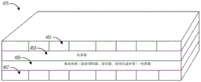
Fig. 4C shows a side view 450 of an example chip embedded DC-DC converter with embedded stacked inductors. The first layer 451 may be, for example, an encapsulation layer or a PCB layer. The second layer 453 may be a PCB layer including an inductor embedded within the second layer 453. The third layer 455 may be a PCB layer including circuitry (e.g., ICs) embedded within the third layer. The circuit (e.g., IC) may include, for example, a PWM controller, a driver, and/or a switch (e.g., a FET switch). The fourth layer 457 may be, for example, an encapsulation layer or a PCB layer. In fig. 4C, the inductor at least partially overlaps or is offset to one side of the circuit (e.g., IC). The inductor may be coupled to the IC by vias and/or traces without the need for wire bonds.
Fig. 4D shows a side view 475 of an example chip-embedded DC-DC converter with embedded inductors. Layers 451, 453, 455, and 457 may be the same or similar to the layers described in fig. 4C. In fig. 4D, layer 455 may include inductors alongside circuits (e.g., ICs) and other circuits (e.g., ICs). The IC may be coupled to the inductor through the trace. Layer 453 can include an embedded capacitor. In some embodiments, one or more embedded capacitors may be embedded in a PCB and may be mounted such that a footprint of the one or more embedded capacitors overlaps a footprint of a circuit (e.g., IC) and/or an inductor. In some embodiments, one or more embedded capacitors may be included in the same layer 455 as the embedded circuit (e.g., IC) and/or the embedded inductor. In some embodiments, the capacitor may be mounted on layer 453. In some embodiments, layer 453 may be omitted. In some embodiments, a capacitor (e.g., capacitor 323 as shown in fig. 3) may be mounted external to the PCB. Many variations are possible. A circuit (e.g., one or more ICs) including any combination of PWM controllers, drivers, and/or switches may be in the same layer as one or both of the one or more inductors and/or the one or more capacitors. The IC may be an gan IC. The monolithic gan IC may include any combination of PWM controllers, drivers, and one or more switches. In some implementations, one or more capacitors and/or one or more inductors may be included in one IC (e.g., an edan IC) with one or more PWM controllers, drivers, and/or one or more switches. The one or more inductors, the one or more capacitors, or both may be disposed in a separate layer embedded in the PCB, such as above or below the circuitry (e.g., ICs). In some embodiments, one or more inductors may be located on a first side of a circuit (e.g., an IC) and one or more capacitors may be located on an opposite second side of the circuit (e.g., an IC). In some embodiments, the one or more inductors and the one or more capacitors may be embedded in different layers of the PCB, but located on the same side of the circuit (e.g., IC). One or both of the one or more capacitors and/or the one or more inductors may be disposed external to the PCB (as shown in fig. 3). In some implementations, the one or more PWM controllers, drivers, and one or more switches may be located in different layers embedded in the PCB. In some embodiments, the PWM controller and the driver may be located in separate ICs (e.g., an edan IC). Components embedded in different layers of the PCB may be oriented such that they at least partially or completely overlap, or do not overlap. Any of the GaN embodiments disclosed herein may also be implemented as GaN embodiments, which may include depletion mode GaN, and/or any combination thereof.
Fig. 5 shows a perspective view 500 of an example chip-embedded DC-DC converter. Fig. 5 shows the same example chip-embedded DC-DC converter as shown in fig. 4A and 4B, but without inductor 321, capacitor 323, or core 311 to illustrate other shaded components. The vias 305 may couple the traces 313 and/or the pads 303.
Fig. 6 illustrates a bottom view 600 of an example chip-embedded DC-DC converter. Fig. 6 shows the same example chip-embedded DC-DC converter as shown in fig. 5. Exposed metal 303 pads between insulator 301 regions provide electrical contacts for power supply voltage, ground, and/or voltage outputs. Vias 305 are shown. However, in some embodiments, the vias through the exposed metal 303 are not clearly visible.
Reduced footprint
The physical arrangements and other techniques disclosed herein may be used to reduce the footprint of a DC-DC converter. In some embodiments, the footprint may be reduced by about 70%. Stacked components, the use of smaller inductors with faster switching speeds, and a single package of components can all reduce the footprint.
As previously mentioned, some DC-DC converter packages do not include inductors or capacitors, and some DC-DC converters may include inductors mounted alongside the driver, PWM controller, and/or IC chip. Such packaging allows the user flexibility in selecting particular values for the capacitors and/or inductors and in controlling the quality of these components. However, stacking the components rather than side-by-side may reduce the footprint of the DC-DC converter. Some embodiments disclosed herein have inductors that are fully or partially vertically stacked on an IC chip. Some embodiments disclosed herein have capacitors that are fully or partially vertically stacked on an IC chip. Stacking inductors and/or capacitors may reduce the footprint of the DC-DC converter. The stacked components may be electrically coupled (e.g., to an IC chip) through vias, which may reduce parasitic effects as described above. Some embodiments disclosed herein may provide a convenient design such that a user does not need to select, set, and install individual components. A single package DC-DC converter may be used without the need to configure external capacitors or inductors. Further, some embodiments may integrate the inductor into the package without affecting the size of the inductor, without affecting the performance of the inductor, and/or without requiring customization of the inductor.
As described above, it is possible to reduce the parasitic effect and effectively increase the switching speed of the DC-DC converter. The inductance of the DC-DC converter can be determined according to equation 2,

wherein L is inductance, V in Is an input voltage, V o Is the output voltage,. DELTA.iL is the inductor ripple current, F s Is the switching frequency. It should be noted that the inductance decreases with increasing switching speed. Thus, the reduced parasitics and faster switch or switches (e.g., an eGaN switch) may allow the DC-DC converter to use smaller inductors. In a DC-DC converter, an inductor is one of the largest components. By reducing the size of the inductor (e.g., to a certain proportion of its original size), the footprint may be substantially reduced.
Some DC-DC converters include multiple packages. For example, there may be a first package including a driver, a second package for a switch, and a third package including an inductor. Some embodiments disclosed herein have a single package that includes all components of the DC-DC converter, such as the PWM controller, the driver, the switch (e.g., the gan switch), the inductor, and the capacitor. In some embodiments disclosed herein, many components, such as PWM controllers, drivers, and/or switches (e.g., gan switches), may be integrated into a single IC.
Therefore, the characteristics related to higher switching speed may also be coordinated with the physical design of the DC-DC converter, so that the size of the DC-DC converter may be reduced. Smaller DC-DC converters may be used in a variety of applications to provide higher current densities to power modern electronic devices (e.g., microprocessors, field programmable gate arrays, application specific integrated processors, etc.). Smaller DC-DC converters can be manufactured at lower manufacturing costs. The techniques disclosed herein may reduce board and package parasitics. Smaller DC-DC converters may have tighter connections, thereby reducing parasitics between inductors, IC chips, and/or loads, and the DC-DC converter may operate efficiently at higher frequencies. The techniques disclosed herein may reduce noise, including reducing ripple effects and reducing electromagnetic interference.
In general, larger size DC-DC converters can handle large amounts of current. In some embodiments, the DC-DC converters disclosed herein may handle a specified amount of current using a smaller sized DC-DC converter as compared to conventional approaches. For example, the footprint of the DC-DC converter disclosed herein may be less than 20mm 2 Current per ampere, less than 15mm 2 Current per ampere, less than 10mm 2 Current per ampere, less than 7mm 2 Current per ampere, less than 5mm 2 Current per ampere, less than 4mm 2 Current per ampere, less than 3mm 2 Current per ampere, less than 2mm 2 Current per ampere, less than 1.5mm 2 Current per ampere, or less than 1mm 2 Per ampere of current. The footprint of the DC-DC converter may be as low as 1.0 or 0.5mm 2 Current per amp, however, values outside the ranges discussed herein may be used in certain implementations.
Example applications
The DC-DC converter disclosed herein may be used to power an electronic device. Examples include using a DC-DC converter to convert a primary supply voltage to a DC voltage suitable for an electronic device powered by the supply voltage. For example, in certain applications, modern power management solutions may use 40 or more chip-embedded DC-DC converters to power 40 or more electronic components while meeting specification requirements of size, input/output ripple, efficiency, and thermal limits. The DC-DC converter disclosed herein can be smaller and used in modern systems with limited space and board size. The DC-DC converters disclosed herein may be used to power components in different market segments (e.g., memory, servers, networks, telecommunications, internet of things, etc.). Other applications include powering micro point-of-load devices (e.g., processors in blade servers, components of solid state devices, etc.) using the DC-DC converters disclosed herein.
Fig. 7A shows an example of a DC-DC converter used for the storage device 700. For example, the storage device 700 may be, for example, a solid state drive. The memory device 700 may include a controller 703 and a plurality of memory chips 705 coupled through a PCB 701. The DC-DC converter 707 may receive a supply voltage via the power input pin 709 and provide DC power to the memory chip 705 and/or the controller 703. DC-DC converter 707 may be coupled to inductor 709 by wire bonds or through traces 711 of PCB 701. The PCB 701 may be a PCB 701 separate from the packaging of the DC-DC converter 707. The capacity of the memory device 700 is limited by the number of memory chips 705, which in the implementation of FIG. 7A are six memory chips.
Fig. 7B shows an example of applying a chip-embedded DC-DC converter to the storage device 750. The chip-embedded DC-DC converter 751 receives a supply voltage through the power input pin 709 and provides DC power to the memory chip 705 and/or the controller 703. The chip-embedded DC-DC converter 751 may include smaller inductors in the footprint of the package. The chip-embedded DC-DC converter 751 may be substantially smaller than the DC-DC converter 707 in fig. 7A. Thus, additional PCB space is available for additional memory chips 753 to increase the storage capacity of memory device 750.
Fig. 8A shows an example application of a DC-DC converter on a circuit board 800. The circuit board 800, which may be, for example, a blade server or motherboard, includes a plurality of power connectors 801 (PWRs), voltage Regulation Management (VRM) circuitry 803, a plurality of Random Access Memory (RAM) slots 805, a plurality of Peripheral Component Interconnect Express (PCIE) slots 813, and a rear input/output panel 815. The circuit board 800 also includes a plurality of DC-DC converters 807 located at the load points. Each DC-DC converter 807 provides power to one of a Central Processing Unit (CPU) 809 or a computer chip 811. The DC-DC converter 807 may receive power supplied through the power supply connector 801 and/or the VRM circuit 803 and convert the voltage of the supplied power into a DC voltage in conformity with the DC power specification of each CPU809 or computer chip 811.
Fig. 8B illustrates an example application of a chip-embedded DC-DC converter on a circuit board 850. The circuit board 850 includes a plurality of chip-embedded DC-DC converters 851 (e.g., at load points). For example, the chip embedded DC-DC converter 851 may provide power to the central processor 809 and/or the computer chip 811. The DC-DC converter 851 may receive power supplied through the power supply connector 801 and/or the VRM circuit 803 and convert the voltage of the supplied power into a DC voltage in compliance with the DC power specification of each CPU809 and/or the computer chip 811. The chip-embedded DC-DC converter 851 may be smaller than the DC-DC converter 807 in FIG. 8A. Thus, the motherboard can accommodate more computer chips 853. The area previously occupied by the DC-DC converter 807 can now be an open area 855 available to other components, which can also be left open to improve airflow.
Other embodiments
In some example embodiments, one or more switches (e.g., an eGaN switch) (e.g., a monolithic or independent switch) may be used in a chip-embedded DC-DC synchronous buck converter with an inductor, where the embedded IC chip includes a PWM controller and a driver. Compared to MOSFET-based DC-DC synchronous buck converters, chip-embedded DC-DC converters can switch at higher speeds with lower switching losses, can switch more efficiently at high switching speeds (e.g., about 5MHz or other speeds described herein), and have the Q of an eGaN switch G Possibly by about five times.
Some embodiments achieve an increase in efficiency gain when switching at the same speed (e.g., 3 MHz), reducing power loss by about 30% compared to alternative designs.
In an example embodiment, a chip-embedded DC-DC converter may be packaged in an approximately 3x3x1.5 mm package, switching in the range of approximately 1-5MHz, and providing approximately 6A current. In contrast, various wirebond DC-DC converter designs with similar amperage have an area of about 12x12 mm and a switching frequency of about 600kHz.
In an example embodiment, the chip-embedded DC-DC converter may receive a 12V power supply and output a DC signal of about 1.2V and about 10A. The switching frequency of the chip-embedded DC-DC converter may be about 1MHz and include an inductance of about 300 nH.
In some example embodiments, the chip-embedded DC-DC converter includes a 25A buck converter that can be mounted in a package of about 6 × 6 mm or 7 × 7 mm.
In some embodiments, the chip-embedded DC-DC converter includes an gan switch. The switch can operate at about 5MHz, and the operating efficiency of the chip-embedded DC-DC converter is close to that of a MOSFET-based DC-DC converter (operating at about 1 MHz). This may result in smaller package size and higher overall system performance due to faster response to transient loads.
Example method
Fig. 9 shows a flow diagram of an example method 900 for manufacturing and using a chip-embedded DC-DC converter.
At block 901, an integrated circuit may be fabricated. The integrated circuit may be an IC chip comprising at least one of: a driver, a PWM controller, and one or more power switches. The IC chip may include a plurality of: a driver, a PWM controller, a power switch, an inductor, a capacitor, or other components of a DC-DC converter. In some embodiments, the one or more power switches may be an eGaN switch, a gallium arsenide switch, or other type of high performance switch.
At block 903, a first PCB portion may be formed. Forming the first PCB portion may include: providing PCB layers or insulators, masking, etching, drilling vias, filling vias, depositing conductive traces and pads, providing partial or full I 2 C andand/or PMBUS, etc.
At block 905, the IC chip may be embedded using chip embedding techniques. In some embodiments, for example, a cavity may be formed (e.g., in a PCB) using machining or etching techniques, and an IC chip may be placed in the cavity. The IC chip may be coupled to the first PCB portion, inside the PCB, on a PCB layer, between multiple PCB layers, between multiple PCBs, and so forth. The IC chip may be a face-up or face-down embedded chip. In some embodiments, the IC is embedded using flip-chip technology. The IC chip or die may be coupled to a die attach or bonding material. In some embodiments, other components may also be embedded in the PCB. For example, in embodiments where one or more switches (e.g., a monolithic gan power switch) are separate from the IC chip, one or more switches (e.g., a monolithic gan switch) may also be embedded in the PCB.
At block 907, insulator and conductive routing for the second portion of the PCB may be formed. This may include providing additional PCB layers or insulators, masking, etching, drilling or exposing vias, filling vias, depositing conductive traces and pads, providing partial or full I 2 C and/or PMBUUS, etc. In some embodiments, the actions described with respect to blocks 903, 905, and 907 may be processed and/or repeated concurrently. In blocks 903, 905, and 907, conductors (e.g., vias and traces) may be formed to couple components in the DC-DC converter device (e.g., as shown in fig. 1 and 3).
At block 909, the inductor may be coupled. The inductor may be coupled to the top of the PCB. The inductor may be at least partially stacked with one or more other components (e.g., IC chips) of the DC-DC converter. The inductor may be at least partially stacked with one or more other components of the DC-DC converter, such as the PWM controller, the driver, and the switch. In some embodiments, other surface components (e.g., capacitors) may also be coupled. Thus, the components of the chip-embedded DC-DC converter may be coupled together. In some embodiments, the inductance of the inductor may be selected based at least in part on the overcurrent limit, for example, as described in fig. 1. In some embodiments, the over-current limit may be determined, adjusted, and/or trimmed based at least in part on the saturation limit of the inductor. In some embodiments, the inductance and overcurrent limits may be determined and/or designed by an individual, designer, design team, and/or manufacturer.
At block 911, the chip embedded DC-DC converter may be packaged. This may include packaging the chip-embedded DC-DC converter as a single discrete component. The package may include inductors and capacitors such that the DC-DC converter may operate without external inductors or capacitors.
At block 913, a load may be coupled to the DC-DC converter. This may include, for example, coupling the output of the packaged chip-embedded DC-DC converter to the electronic device through traces on a separate motherboard. In some embodiments, the DC-DC converter may be coupled near the point of load to reduce some parasitics.
At block 915, a power supply may be coupled to the packaged chip-embedded DC-DC converter. Therefore, the chip-embedded DC-DC converter can provide a DC output voltage by using the provided power to supply power to the electronic equipment.
Although blocks 911, 913 describe a packaged and chip-embedded DC-DC converter using a separate PCB with a load device, in some embodiments, the techniques described herein may be applied to a terminal device PCB.
Chip embedded DC-DC converter with multiple inductors
The chip-embedded DC-DC converter techniques described herein may be extended to multi-inductor implementations. This may include, for example, dual buck converters, dual boost converters, and voltage converters (with 2, 3, 4, 5, 6, 8, 16, or any number of inductors). Multiple inductors may be arranged in parallel. The outputs of the multiple inductors (e.g., in a parallel arrangement) may be coupled to a tank circuit, such as a capacitor or an LC resonant circuit. Each inductor may be coupled to a corresponding pair of switches. Each respective pair of switches may be driven by a respective driver. Each driver may be driven using a PWM signal that is out of phase with the PWM signal provided to the other drivers. Each PWM signal may have an on-time that is a sufficiently small fraction of the sharing period such that the superimposed combination of drive signals has an active period that is shorter than the sharing period. In some embodiments, a multi-inductor chip embedded DC-DC converter may be formed by duplicating some or all of the components (e.g., switches, inductors, components of an integrated circuit) disclosed herein (e.g., shown in fig. 1).
Various embodiments disclosed herein may have one, some combinations, or all of the following features. The multi-inductor chip-embedded DC-DC converter has higher operation speed and higher efficiency than the single-inductor chip-embedded DC-DC converter. The current through the DC-DC converter may be divided between a plurality of inductors. Heat may be dissipated across multiple inductors. A single sensor of smaller size may be used. The current density can be increased. The overall size of the DC-DC converter can be reduced. The number of times of switching of the switch can be reduced. The life expectancy of the switch can be extended. The life expectancy of the inductor can be improved. A smaller and/or smaller number of output capacitors may be used. The transient response speed may be faster. When the current demand varies, the fluctuation of the output voltage may be small. The DC-DC converter may operate at a higher frequency and/or use a smaller inductor (e.g., according to equation 2). The size of the DC-DC converter can be reduced. Each pair of switches can operate at the maximum effective frequency, but the total frequency can be greater than the individual frequencies of any pair of switches.
In some embodiments, power loss may be reduced. Using the equation P = I 2 * R, it can be seen that the power loss increases with increasing DC current (I). However, by shunting current between multiple inductors, the overall power loss can be reduced. In addition, the resistance of each inductor is also reduced. For example by shunting current (I) between two inductors O ),P=2*[(I O /2)2*R/2]=[I O 2 *R]And/2, it can be seen that the power loss can be reduced by half. Thus, distributed power transfer between multiple inductors may improve efficiency. With the increasing demand for high current density DC-DC converters, the multi-inductor chip embedded DC-DC converter can provide a small size, high currentDensity and low power consumption.
In some embodiments, a smaller inductor in a multi-inductor chip embedded DC-DC converter can make a faster transient response to changes in the required current. For example, as shown in fig. 8B, a chip-embedded DC-DC converter may provide DC power to the CPU. The CPU may suddenly experience a large computational load (e.g., utilize all of the cores and/or increase its switching frequency), resulting in a sudden increase in power consumed (e.g., from 1 amp to 10 amps in the ns range). Since the energy comes from the output capacitor (e.g., output capacitor 111 in fig. 1, 2), the voltage across the output capacitor may drop too quickly, exceeding the DC power supply specification required by the CPU (e.g., <1% voltage drop), possibly resulting in a shutdown error. Accordingly, a feedback system (e.g., as shown in fig. 14, 16, and 17) may be implemented to increase the power delivered to the capacitor through the inductor and prevent voltage drops. However, the high inductance resists variations in power transfer. Because the multi-inductor system employs a smaller inductor, the transient feedback response of the multi-inductor chip-embedded DC-DC converter is faster and has a lower output voltage drop than the transient feedback response of a DC-DC converter with fewer, larger inductors. The DC-DC converters disclosed herein with higher switching frequencies may use smaller inductors, and thus, in the embodiments described herein, a single inductor may respond faster to transient loads.
Example Dual Buck converter
Fig. 10 shows an example dual inductor design for a dual buck converter 1000 using a chip embedded DC-DC converter. A dual buck converter may use two parallel inductors instead of a single inductor.
Fig. 10 includes a first inductor 1001, a second inductor 1003, and a PCB 1005, the PCB 1005 including a chip embedded IC and other components (shown in fig. 11A, 11B, 11C, and 11D, not visible in fig. 10). The first input node 1007A of the first inductor 1001 may correspond to a first pad 1007B on the PCB 1005. A second input node 1009A of the second inductor 1003 corresponds to a second pad 1009B on the PCB 1005. Voltage output node 1011A corresponds to voltage output pad 1011B on PCB 1005. Graph 1013 shows waveforms of signal 1, signal 2, and an output signal.
A dual buck converter may be configured to include two inductors 1001, 1003. Two inductors 1001, 1003 may be mounted on a PCB 1005. In various embodiments, the two inductors 1001, 1003 may be two independent inductors placed side by side, two independent inductors stacked vertically (one on top of the other), or a single magnetic core with two inductor windings.
Fig. 12 shows an example circuit level schematic 1200 of a dual buck converter including a chip embedded DC-DC converter. The schematic includes a voltage source 1201, a first switch 1203 of a first switch pair, a second switch 1205 of the first switch pair, a third switch 1207 of a second switch pair, a fourth switch 1209 of the second switch pair, a first inductor 1211, a second inductor 1213, an output capacitor 1217, and a voltage output node 1219.
A voltage source 1201 may be coupled to a drain of the first switch 1203. A source of the first switch 1203 may be coupled to a first node of the first inductor 1211. The source of the first switch 1203 may also be coupled to the drain of the second switch 1205. The gates of the first switch 1203 and the second switch 1205 may be coupled to a driver (not shown in fig. 12). The driver may drive opposite control signals to the first switch 1203 and the second switch 1205 to alternately turn on and off the first switch 1203 and the second switch 1205, causing one of the first switch 1203 and the second switch 1205 to be turned on and the other to be turned off. When the first switch 1203 is turned on and the second switch 1205 is turned off, energy may be provided from the voltage source 1201 to the inductor 1211 and/or the capacitor 1217, and the energy may be stored in the inductor 1211 and/or the capacitor 1217, thereby causing the output voltage to increase. When the first switch 1203 is turned off and the second switch 1205 is turned on, energy may be released from the inductor 1211 and/or the capacitor 1217, causing the output voltage to drop.
A voltage source 1201 may be coupled to the drain of the third switch 1207. A source of the third switch 1207 may be coupled to a first node of the second inductor 1213. The source of the third switch 1207 may also be coupled to the drain of the fourth switch 1209. The gates of the third and fourth switches 1207 and 1209 may be coupled to a driver (not shown in fig. 12). Accordingly, the driver may drive opposite control signals to the third switch 1207 and the fourth switch 1209, thereby alternately turning the third switch 1207 and the fourth switch 1209 on and off, causing one of the third switch 1207 and the fourth switch 1209 to be turned on and the other to be turned off. When the third switch 1207 is turned on and the fourth switch 1209 is turned off, energy may be provided from the voltage source 1201 to the inductor 1213 and/or the capacitor 1217, and energy may be stored in the inductor 1213 and/or the capacitor 1217, resulting in an increase in the output voltage. When the third switch 1207 is turned off and the fourth switch 1209 is turned on, energy may be discharged from the inductor 1213 and/or the capacitor 1217, resulting in a drop in the output voltage.
A second node of the first inductor 1211 and a second node of the second inductor 1213 may be coupled to an output node 1219, and may also be coupled to an output capacitor 1217 (also referred to as a smoothing capacitor). The voltage at the output node 1219 may be affected by the energy stored in the capacitor 1217. When current from the capacitor 1217 flows from the second node of the first inductor 1211 or the second node of the second inductor 1213, the energy stored in the capacitor 1217 may increase. Thus, a small signal ripple is provided to the capacitor when the switch supplies or releases energy.
The first pair of switches 1203, 1205 may be driven out of phase with the second pair of switches 1207, 1209. The first pair of switches 1203, 1205 may also be driven at the same frequency and period as the second pair of switches 1207, 1209. Thus, in some embodiments, at most one of the switches 1203, 1207 is turned on at a specified time. The four switches 1203, 1205, 1207, 1209 may be driven by four separate signals, which are out of phase with each other. The first pair of switches 1203, 1205 and the first inductor 1211 provide a DC suppression function simultaneously with the second pair of switches 1207, 1209 and the second inductor 1213.
Fig. 13A shows an example circuit level schematic 1300 of a DC-DC converter including a chip-embedded DC-DC converter. The components in fig. 13A may be the same as or similar to the components in fig. 12. The DC-DC converter in fig. 13A may include an additional capacitor 1221. When the switch 1203 is turned on, the capacitor 1221 may store energy. In some embodiments, energy may be stored, charging capacitor 1221 to about half the voltage of power supply 1201. When switch 1203 is on, switch 1207 is off, switch 1205 is off, and a transient current may flow through capacitor 1221 to inductor 1211. When switch 1207 is on and switch 1209 is off, capacitor 1221 supplies power to switch 1207, causing current to flow to inductor 1213. Capacitor 1221 also acts as an AC coupling capacitor between switch 1207 and switch 1205. The assembly in fig. 13 is also provided in a modified arrangement compared to the assembly in fig. 12, but the DC-DC converter in fig. 12 and 13A can operate similarly. Inductors 1211 and 1213 may use a shared common core or may use separate cores.
Fig. 13B shows an example circuit level schematic 1350 of a DC-DC converter including a chip-embedded DC-DC converter. The components in fig. 13 may be the same as or similar to the components in fig. 12. The first pair of switches 1203, 1205 and the first inductor 1211 may be coupled to a first capacitor 1217A and configured to provide a first output voltage at a first output node 1219A. The second pair of switches 1207, 1209 and the second inductor 1213 may be coupled to a second capacitor 1217B and configured to provide a second output voltage at a second output node 1219B. The output voltages at the first and second output nodes 1219A, 1219B may be the same voltage or different voltages. In some embodiments, a driver (e.g., as shown in fig. 1, not shown in fig. 13B) may drive the first and second pairs of switches 1203, 1205, 1207, 1209, respectively, such that different voltages are provided at different nodes 1219A, 1219B. Inductors 1211 and 1213 may use a shared common core or may use separate cores.
The embodiment shown in fig. 13A and 13B may be implemented on one or more IC dies. For example, in fig. 13A, switches 1203, 1205, 1207, 1209 may all be contained in a single IC (e.g., a monolithic gan IC). In some embodiments, the switches 1203, 1205, 1207, 1209 may be allocated between two or more separate devices. The embodiments shown in fig. 13A and 13B may also be controlled by one or more drivers and/or PWM controllers. For example, a first PWM controller may be coupled to a first driver that drives a first pair of switches 1203, 1205, 1207, 1209, and a second PWM controller may be coupled to a second driver that drives a second pair of switches 1203, 1205, 1207, 1209.
Example design for embedding a chip in a Dual Buck converter
FIG. 11A shows a first example layout design 1100 of an embedded chip in a dual buck converter. The design includes an IC portion 1101, a first power switch 1103 of a first switch pair, a second power switch 1105 of the first switch pair, a third power switch 1107 of the second switch pair, and a fourth power switch 1109 of the second switch pair.
In the embodiment of fig. 11A, IC portion 1101, first power switch 1103, second power switch 1105, third power switch 1107, and fourth power switch 1109 are all contained within the same IC chip. IC portion 1101 may include a PWM controller and a driver. The driver may be configured to drive the first switch pair and the second switch pair out of phase. The driver may be configured to drive the first switch pair and the second switch pair with the same period and the same frequency. The driver may also be configured to alternately drive the switches in each pair of switches. In some embodiments, IC portion 1101 includes a first driver configured to drive a first switch pair, and a second driver configured to drive a second switch pair. The PWM controller may provide a first PWM signal to the first driver, a second PWM signal to the second driver, and the first and second PWM signals may be out of phase with each other.
FIG. 11B illustrates a second example layout design 1120 of an embedded chip in a dual buck converter. The design includes an IC chip 1121, a first power switch 1123 of a first switch pair, a second power switch 1125 of the first switch pair, a third power switch 1127 of a second switch pair, and a fourth power switch 1129 of the second switch pair.
The first power switch 1123 and the second power switch 1125 may be part of a first monolithic switch chip (e.g., a monolithic eGaN switch chip). The third power switch 1127 and the fourth power switch 1129 may be part of a second monolithic switch chip. In some embodiments, the first monolithic switch pair and the second monolithic switch pair may be part of the same monolithic chip. In some embodiments, the first monolithic switch pair and the second monolithic switch pair may be separate monolithic chips. The IC chip 1121 and the separate monolithic chip may be embedded in a PCB. The IC portion 1121 may include a PWM controller and a driver. The driver may be configured to drive the first monolithic switch pair and the second monolithic switch pair out of phase. The driver may be configured to drive the first and second monolithic switch pairs with the same period and the same frequency. The driver may also be configured to alternately drive the switches in each monolithic switch pair. In some embodiments, IC portion 1121 includes a first driver configured to drive a first pair of monolithic switches, and a second driver configured to drive a second pair of monolithic switches. The PWM controller may provide a first PWM signal to the first driver, a second PWM signal to the second driver, and the first and second PWM signals out of phase with each other.
Fig. 11C shows a third example placement design 1140 of an embedded chip in a dual buck converter. The design includes an IC chip 1141 portion, a first power switch 1143 of a first switch pair, a second power switch 1145 of the first switch pair, a third power switch 1147 of a second switch pair, and a fourth power switch 1149 of the second switch pair.
The IC chip portion 1141, the first power switch 1143, and the third power switch 1147 may be part of a first IC chip. The second power switch 1145 and the fourth power switch 1149 may be separate chips from the first IC chip (e.g., a separate monolithic gan chip). In some embodiments, the second power switch 1145 and the fourth power switch 1149 may be part of the same monolithic chip. One, some or all of the chips may be embedded in the PCB. The IC portion 1141 may include a PWM controller and a driver. The driver may be configured to drive the first switch pair and the second switch pair out of phase. The driver may be configured to drive the first switch pair and the second switch pair with the same period and the same frequency. The driver may also be configured to alternately drive the switches in each pair of switches. In some embodiments, the IC portion 1141 includes a first driver configured to drive the first switch pair, and a second driver configured to drive the second switch pair. The PWM controller may provide a first PWM signal to the first driver, a second PWM signal to the second driver, and the first and second PWM signals out of phase with each other.
FIG. 11D illustrates a fourth example layout design 1160 of an embedded chip in a dual buck converter. The design includes an IC chip portion 1161, a first power switch 1163 of a first switch pair, a second power switch 1165 of the first switch pair, a third power switch 1167 of a second switch pair, and a fourth power switch 1169 of the second switch pair.
Various additional arrangements may be made such that components 1161, 1163, 1165, 1167, and 1169 may be arbitrarily combined into any number of IC chips. In some embodiments, a multi-inductor DC-DC converter may be created by combining the individual packages of single or multiple inductor DC-DC converters.
Other example features of a multi-inductor chip-embedded DC-DC converter
In some chip-embedded DC-DC converters, the inductor is the largest physical component. While a multi-inductor chip-embedded DC-DC converter may use multiple smaller parallel coupled inductors. The switches may be driven out of phase such that the multiple inductors charge and discharge energy out of phase. In some embodiments, the outputs of the plurality of inductors are coupled in parallel such that the frequency of the output ripple of the plurality of inductors is higher than the frequency of the output ripple of any single inductor. In some embodiments, the outputs of the plurality of inductors are coupled in parallel, and the output ripple of the plurality of inductors has the same period as the output ripple of the single inductor.
In some embodiments, the output ripple frequency of a multi-inductor DC-DC converter may be higher, and the number and/or capacitance of output capacitors may be reduced, and smaller output capacitors may be used.
As described above, a system of multiple inductors has a higher effective switching speed than a system of single inductors. In some embodiments, this may be done without increasing the switching speed of the switch; instead, the multiple switches may operate out of phase with each other. Thus, a higher effective switching speed is achieved without advancing the switching speed of the individual switches to a higher and inefficient level.
According to equation 2, since the effective switching speed of the plurality of inductors disposed in parallel is high, the inductance of the plurality of inductors can be reduced. Thus, inductors may be placed in parallel to reduce inductance, and/or smaller inductors with smaller inductances may be used. Since smaller inductors can be used, the size of the whole DC-DC converter can be reduced, especially when the inductor is the largest component.
In some embodiments, the use of smaller inductors may produce further synergy: the switching speed of the switch may increase because the inductive load of the switch is reduced. This may result in a faster effective switching speed, further reducing inductance according to equation 2, and so on.
In some embodiments, a multiple inductor, chip-embedded DC-DC converter may use a smaller output capacitor than the output capacitor in a single inductor DC-DC converter.
Examples of chip-embedded DC-DC converters with feedback
Fig. 14 shows an example chip-embedded DC-DC converter 1400 with an external ripple voltage feedback circuit. As discussed herein, chip embedded DC-DC converter 1400 may include an embedded IC chip 1403, and embedded IC chip 1403 may include a driver and/or a modulator. The IC chip may be embedded in PCB 1401. The chip-embedded DC-DC converter 1400 further includes a first power switch 1405, a second power switch 1407, and an inductor 1409. The inductor 1409 is schematically represented to show its inductive component 1411 and its internal Direct Current Resistance (DCR) component 1413.
The chip-embedded DC-DC converter 1400 receives an input voltage at a voltage input node 1415 and provides an output voltage at an output voltage node 1417. An output capacitor 1421 is coupled to the output node 1417, the output capacitor being schematically represented to show its capacitive component 1423 and its Equivalent Series Resistance (ESR) 1425. A feedback path 1427 is coupled from the output node to embedded IC chip 1403.
As previously described, the chip-embedded DC-DC converter 1400 may receive an input voltage and may generate an output voltage. When the switch is turned on and off, the output voltage may beThere will be small fluctuations or ripples. Ripple voltage (V) ESR ) Can be controlled by applying an inductive current I L Multiplied by the ESR. Feedback path 1427 senses ripple and/or DC output voltage. A feedback indication of the ripple and/or the dc output voltage is provided to the embedded IC chip 1403. The modulator in embedded IC chip 1403 may utilize feedback to control switches 1405, 1407 to lower the output voltage when it is too high and to raise the output voltage when it is too low.
The feedback system may use a current mode control scheme and a voltage mode control scheme to ensure operational stability of the DC-DC over many different duty cycles. In existing mode control schemes, a slope compensation scheme may be used and implemented with external components that may increase size and cost. Current mode control schemes may use type II compensation to achieve loop stability and may have slower loop response. In a voltage mode control scheme, the voltage error can be amplified, fed back and compensated.
In some embodiments, the modulator may use a constant on-time frequency modulation scheme, a constant off-time frequency modulation scheme, a pulse width modulation scheme, or other scheme. The constant on-time and constant off-time schemes can provide stable DC-DC operation with high performance. In some embodiments, it is desirable for the modulator to be able to detect the ripple voltage to trigger certain control events. For example, in a constant on-time scheme or a constant off-time scheme, the modulator may detect AC ripple to generate on or off pulses with constant on or off times, respectively, to modulate the frequency and affect the period of the control signal sent to the switches 1405, 1407. For example, in a constant on-time scheme, a fixed width on-pulse may be provided to increase the output voltage in response to detecting a lower output voltage compared to a reference voltage, and/or in response to detecting a sufficient amount of inductor current ripple. Thus, for a constant on-time scheme, each pulse has the same duration in the on state, and modulation is achieved by performing more or less pulses at a time (e.g., the off-time between pulses may vary). Constant closingThe off-time scheme may be similar to the constant on-time scheme described herein, except that the off-time between pulses is constant and modulation may be achieved by the width of the on-pulse. In another example of a voltage mode system, the frequency may be fixed and the duty cycle of the pulses may be modulated. The variations may include leading edge or trailing edge modulation schemes. Any suitable modulation scheme may be used. Accordingly, ESR 1425 may be designed and/or selected such that the modulator is able to detect a sufficiently large V ESR 。
Some embodiments disclosed herein provide solutions to some conflicting design challenges. The non-delayed feedback path may respond quickly to changes in the output voltage. The feedback path may be used for certain modulation/control schemes, such as constant on-time or constant off-time schemes, to control when the switches 1405, 1407 are turned on or off. In order to provide a measurable large V along the feedback path ESR The signal (which can be reliably detected by the modulator), the ESR 1425 of the capacitor 1421 can be designed and/or selected so as to produce a sufficiently large ripple. At the same time, the ripple voltage can be minimized. A DC-DC converter may ideally produce a pure DC voltage. In practice, many applications allow small ripples to be generated on the output of a DC-DC converter, but only to a small extent. Certain devices powered by a DC power supply may require a maximum of 3% ripple, 2% ripple, 1% ripple, 0.5% ripple, 0.1% ripple, 0.05% ripple, 10mV ripple, 5mV ripple, 3mV ripple, 1mV ripple, 0.5mV ripple, a lesser amount of ripple, or a small amount of ripple that cannot be detected, or any range of ripple defined by any of these values, although values outside of these ranges may be used in some cases. For example, some point-of-load devices may provide for a DC power supply that provides a 1.00V DC output with a ripple or variation that does not exceed 1% (10 mV) of the 1.00V value. A very low ESR capacitor can be used to achieve a low ripple output. However, if the ripple is too low, the modulator may not be able to operate based on ripple feedback (e.g., the modulator may not be able to distinguish between ripple and noise, may operate unstably, etc.).
The present disclosure includes some embodiments of a DC-DC converter that uses a ripple triggered modulator, a low ESR capacitor, and provides a low ripple DC output.
Example Current and ripple plot
FIG. 15 shows the inductor current I L And equivalent series resistance voltage V ESR Example graphs 1500, 1550 of (also referred to as ripple voltage) over time. Line 1501 represents the current I through inductor 1409 of fig. 14 L . Line 1551 represents the output ripple voltage V at node 1417 of FIG. 14 ESR 。
When the switch 1405 is on and the switch 1407 is off, the inductor current I L And (4) increasing. I.C. A L Increased according to the following equation:

wherein, V in Is an input voltage, V out Is the output voltage, L is the inductance, T on Is the time that the switch 1405 is on, I o Is the initial current.
When the switch 1405 is turned off and the switch 1407 is turned on, the inductor current I L And decreases. I is L Decrease according to the following equation:

wherein, V out Is the output voltage, L is the inductance, T off Is the time that the switch 1405 is off, I o Is the initial current. Equations 3 and 4 are an applied version of the general equation (V = L (dI/dt)), where V is the voltage across the inductor and dI/dt is the rate of change of the current with respect to time.
According to equations 3A and 4A, the rate of change of the current can be determined from the time derivative, such as:


V ESR with the inductor current I L Fluctuating up and down. However, with different slew rates (e.g., different slopes), V ESR And I L Increase and decrease. The rate difference is affected by the ESR of capacitor 1421. According to the equation V = I R ESR The voltage can be passed through the inductive current I L Multiplied by the ESR. Therefore, the temperature of the molten metal is controlled,


when the current I is as shown in example diagrams 1500, 1550 L When increasing and decreasing, V ESR Also at the same time, but at different slew rates (different slopes). According to equation V ESR =I L *ESR,V ESR Is proportional to and affected by the ESR. Thus, for low ESR values, even I L Very large, V ESR May also be small. For example, the inductor current I L 3.0A, ripple is 50%, so the fluctuation range is 1.5A to 4.5A, and amplitude is 3.0A. V if the low ESR is 1 m.OMEGA. ESR May fluctuate between-1.5 mV to 1.5mV, which may be too small for some modulators and/or difficult to use reliably. Furthermore, when the current remains positive, V ESR Alternating between positive and negative values.
Example Low ESR, low ripple, chip Embedded DC-DC converter
Fig. 16 shows an example chip-embedded DC-DC converter with an external ripple voltage feedback circuit 1600. The embodiment of fig. 16 may include a PCB 1601, a driver 1603, a first power switch 1605 (e.g., an gan switch), a second power switch 1607 (e.g., an gan switch), an inductor 1609, an output capacitor 1621, and an output node 1617. Fig. 16 also includes a resistor 1643, a capacitor 1645, an AC bypass capacitor 1647, a feedback path 1627, a comparator 1629 and an and gate 1631, a one-shot circuit 1633, an inverter 1635, a minimum delay counter 1637, a resistor 1639 and a resistor 1641.
To sense ripple and provide a feedback voltage, a resistor 1643 may be connected in series with a capacitor 1645, and the series combination of resistor 1643 and capacitor 1645 may be connected in parallel across an inductor 1609. The capacitor 1645 blocks the DC signal. AC signals, such as ripple, can still be sensed. The capacitor 1645 and the resistor 1643 form a voltage divider of the AC signal, and the sensed ripple may pass through an AC bypass capacitor 1647 to the feedback path 1627. The values of the resistor 1643 and the capacitor 1645 may be set so as to satisfy equation 5:

where L is the inductance of inductor 1609, DCR L Is the direct current resistance ("DCR"), R of inductor 1609 x Is the resistance of resistor 1643, C x Is the capacitance of the capacitor 1645. Thus, a circuit may be provided to measurably and reliably sense the inductor current ripple independent of the ESR value.
Resistors 1639 and 1641 may form a voltage divider coupled to output node 1617. The voltage divider may divide the voltage output at the output node 1617. In some embodiments, because of the low ESR of the output capacitor 1621, the ripple at the output node 1617 may be small, difficult to detect, within a noise threshold, or unreliable for modulation. Thus, the voltage divider functions primarily as a DC voltage divider.
The output of comparator 1629 may be provided to one-shot circuit 1633, which generates a constant on-time PWM signal that may be provided to driver 1603. The output of one shot circuit 1633 may also be provided to inverter 1635, minimum turn off delay circuit 1637, and gate 1631 to prevent the PWM signal from continuing high.
The configuration of the resistor 1643, capacitor 1645, and AC bypass capacitor 1647 may result in a significant, measurable ripple being detected and injected into the feedback path 1627 despite the low ESR and low output ripple of the capacitor 1621. Therefore, the detected ripple may be larger than the output ripple. The AC ripple injected into feedback path 1627 may be expressed as:

wherein, V cx Is the ripple voltage on the capacitor 1645, I L Is the peak-to-peak current ripple, R, of the inductor x Is the resistance of resistor 1643, C x Is the capacitance of the capacitor 1645.
In some embodiments, PCB 1601 and its internal components may be packaged and a user may provide and/or configure a circuit that includes inductor 1609, resistor 1643, capacitor 1645, capacitor 1621, capacitor 1645, AC bypass capacitor 1647, resistor 1639, and resistor 1641. In such embodiments, the values of inductor 1609, resistor 1643, and/or capacitor may be selected and adjusted according to equation 6. For example, if the inductor 1609 is changed for a certain application (e.g., having a different inductance and/or DCR), the user can solve equation 6 and then select, obtain, and change the resistor 1643 and/or the capacitor 1645 to correspond to the new L and DCR of the inductor 1609 L The value is obtained.
In some embodiments, some or all of the components shown in fig. 16 may be contained in a single package. In some embodiments, including some, but not all, of resistor 1643, capacitor 1645, and inductor 1609 in one package limits the ability to tune the circuit, according to equation 6. For example, if resistor 1643 and capacitor 1645 are included in the package, but the end user selects inductor 1609, it may limit the end user to using only those with a particular L and DCR L The value of the particular inductor to satisfy equation 6. In such a system and any improperly tuned system, selecting an improper inductor 1609 can cause the system to become unstable and/or to malfunction, which can damage components receiving power from the DC-DC converter. In some cases it may be desirable to properly tune the DC-DC converter as notRequiring a single packaged device to be modified by the end user. Some embodiments disclosed herein may include inductor 1609, resistor 1643, and capacitor 1645 as a single package.
Exemplary Low ESR, low ripple DC-DC converter
Fig. 17 shows an example DC-DC converter 1700 (which may be a chip-embedded DC-DC converter in some embodiments) with an internal ripple voltage feedback circuit. The chip-embedded DC-DC converter 1700 includes a package 1701, a driver 1703, a first power switch 1705, a second power switch 1707, and an inductor 1709, which may be similar to other embodiments described herein. The DC-DC converter 1700 may receive an input voltage at a voltage input node 1715 and may provide an output voltage at an output voltage node 1717. An output capacitor 1721 (e.g., a low ESR output capacitor or multiple capacitors in parallel with low ESR) can be coupled to the output node 1717. A feedback path 1727 may be coupled from the output node to the comparator 1729. The comparator output may be coupled to an and gate 1731 and a one shot circuit 1733, providing the PWM signal to a driver 1703. The ramp generator 1751 may model the inductor ripple current (e.g., model the current 1501 in fig. 15) and output a voltage representation of the ripple current (e.g., 1551 in fig. 15). In some embodiments, the output of the ramp generator 1751 may be combined (e.g., added or subtracted) with a reference voltage at the signal combiner 1753. In some embodiments, the inductive ripple signal output by the ramp generator may be added to the feedback signal instead of being subtracted from the reference voltage. The comparator 1729 may compare the ripple signal output by the ramp generator 1751 with a reference voltage. The comparison results may be used in a feedback loop to drive the system (e.g., switches 1705 and/or 1707).
The inductor 1709 may be included in a chip-embedded DC-DC converter package, as shown in fig. 1, 3, 4A, and 4B. A low ESR output capacitor 1721 may be coupled to the output node 1717. The at least one output capacitor 1721 may have a low ESR (e.g., similar to the values and ranges of the embodiment in fig. 16 discussed herein). For example, the ESR may be in the m Ω range (e.g., 1m Ω, 10m Ω, 100m Ω), or less, and in the μ Ω range (e.g., 10 μ Ω, 100 μ Ω), placing capacitors in parallel may further reduce the effective parallel ESR. The output voltage may have low or no AC ripple (e.g., similar to the values and ranges in fig. 16 discussed herein), enabling the DC-DC converter to meet low ripple output specifications required by certain devices. However, such low AC ripple may be small, difficult to detect, within a noise threshold, non-existent, or unreliable for modulation purposes (e.g., due to low ESR of the output capacitor 1721), and difficult to use for modulation purposes. Through feedback path 1727, a DC output voltage is provided on feedback path 1727 (e.g., along with any small (but not reliably measurable) AC ripple or no AC ripple at all).
The ramp generator 1751 models the inductor ripple independently of the capacitor 1721 and/or its ESR. An example ramp generator is described below with reference to fig. 18. The inputs to the ramp generator may include an input voltage, an output voltage, a switching signal, and an inductance value. The output of the ramp generator 1751 may be combined with a reference voltage for comparison with the voltage on the feedback path 1727, or the output of the ramp generator 1751 may be combined with the voltage on the feedback path 1727 for comparison with a reference voltage. For example, the voltage reference may be provided by a DAC. The DAC may generate a voltage output based on the digital input. Therefore, the DAC voltage can be adjusted in small increments. For example, the output voltage of a 9-bit DAC is adjustable in increments of 5mV. The DAC may be used to set and/or adjust the output voltage of the DC-DC converter. Other examples of voltage references include crystals, bandgap references, batteries, etc., any of which may not be enabled. The reference voltage combined with the simulated inductor ripple may be provided to the input of a comparator 1729, as shown in fig. 17.
The ramp generator 1751 may be contained in a package. The ramp generator 1751 may be included in a chip-embedded IC along with the driver 1703 and other components. The inductor may also be contained within the package. The ramp generator 1751 may be tuned and configured for a particular inductor 1709 selected within the package before the package is provided to a user. Instead of allowing a user to select a design of inductors with different characteristics, a designer selecting packaged inductors 1709 mayKnowing the value and characteristics of the inductor allows the designer to extract and/or determine the slew rate of the inductor 1709 and replicate the slew rate using the ramp generator 1751. In some embodiments, the system does not use the actual ripple signal (e.g., at the inductor) in the feedback loop, but uses a ramp generator to model the ripple signal (e.g., present at the inductor). The ramp generator 1751 may be based on the input voltage V in 、V out The value of L (which may be a known value when the inductor is integrated into the DC-DC converter package) and the switching signal SW to determine the analog ripple signal. The switch signal may indicate the state of one or both of the switches 1705, 1707 and/or the time at which one or both of the switches 1705, 1707 changes state (e.g., HS and LS signals). Since the ramp generator knows the inductance, the input and output voltages, and the timing of the switches, it is able to determine an analog ripple signal that simulates the actual ripple signal (e.g., ripple at the inductor) in the circuit. The analog ripple may be proportional to the ripple in the inductor. The analog ripple may change at the same slope (e.g., at the same rate) as the slope of the ripple change in the inductor. The simulated ripple in the system with the low ESR capacitor 1721 can simulate the ripple that may occur at node 1417 of fig. 14 when the low ESR capacitor 1421 is not used.
An inductive ripple signal may be generated that accurately reflects the ripple through the inductor 1709. By using a ramp generator to generate the inductive ripple signal, a minimum capacitor ESR is not necessary for sensing/detecting the AC ripple. Thus, the output voltage may be a cleaner DC signal with little or no AC ripple.
In some embodiments, the comparator compares the output of the DC-DC converter with a combination of the reference signal and the analog inductive ripple. For example, in a constant on-time modulation scheme, the comparator may output a high signal when the output signal on the feedback path 1727 is below the value of the reference voltage combined with the simulated inductive ripple. A high signal may be provided to the one shot circuit through an and gate, which provides a constant on-time PWM pulse to the driver 1703, which drives switch 1705 on and switch 1707 off. By ensuring that the switch 1705 is periodically turned off and the switch 1707 is periodically turned on, the inverter 1735 and the minimum off-time delay circuit 1737 coupled to the and gate may prevent the one shot circuit 1733 from triggering too frequently. Driving the switch based on the output of the comparator 1729 may be implemented in various other ways.
Although the operation of the circuits in fig. 16 and 17 are described with respect to a constant on-time modulation scheme, it is to be understood that the teachings and disclosure herein are applicable to any voltage mode modulation scheme, such as a constant off-time scheme with appropriate modifications to the circuit (e.g., changing the minimum off-time delay to the minimum on-time delay, making certain comparisons, and/or possibly inverting signals, etc.). Further, the teachings and disclosure herein may also be applied to current mode modulation schemes or voltage modulation schemes.
Fig. 18 shows an example circuit level schematic of ramp generator 1800. Ramp generator 1800 may include a first current source 1801, a second current source 1803, a capacitor 1805, a ramp voltage output node 1807, a first switch 1809, a second switch 1811, a trim controller 1813, and resistors 1815A, 1815B. Trim controller 1813 and/or current sources 1801, 1803 may be coupled to I 2 C and/or PMBUS to receive trim and/or adjust commands.
The ramp generator may be configured to generate an output according to the following equation:


wherein, V ramp-ON And V ramp-OFF Respectively, the on and off voltages (output is the inductor ripple output of ramp generator 1751 in fig. 17), k may be a constant fixed factor, V in Is the input voltage (e.g., the voltage provided at node 1715 in FIG. 17), V out Is the output voltage (e.g., the voltage provided at node 1717 in FIG. 17), where k isValue measured in units of amperes per volt, C ramp Is the capacitance of the capacitor 1805, t on Is the amount of time that the DC-DC converter supplies power to the inductor (e.g., when switch 1809 is closed and switch 1811 is open), t off Is the amount of time that the DC-DC converter is not supplying power to the inductor (e.g., when switch 1809 is open and switch 1811 is closed), V o Is the starting voltage. The ripple voltage slew rate (also known as "slope", in volts/second) is determined by the time period (t) on ,t off ) The coefficient multiplied by the following equation represents:


equations 7 and 8 alone do not show how to set the value of k to model the voltage associated with the inductive ripple, which should depend on the inductance of inductor 1709. Equation 7B and equation 3C may be set equal if the ramp generator is configured to model the slew rate in equation 3C, where C is ramp Is set equal to C x And selecting the resistance R eq To replace R ESR So that:


thus, the value of k can be determined and will be a constant when the capacitance of capacitor 1805, the resistance of resistors 1815A, 1815B, and the inductance of inductor 1709 are fixed. Further, the relationship between k and inductance shows an inverse relationship. If the inductance of inductor 1709 is known, a constant value k can be determined. Accordingly, the inductance of inductor 1709 may be measured, and the ramp generator may be trimmed and/or configured.
The first current source 1801 may be a voltage controlled current source 1801. The output of the voltage controlled current source 1801 may be at least partially defined by V in Voltage and k control. In some embodiments, the output of the voltage controlled current source may be from V in The voltage is controlled by multiplying k. Thus, current source 1801 may be trimmed to decrease the output current when L increases and k decreases, and current source 1801 may be trimmed to increase the output current when L decreases. A current source 1801 is coupled to the first switch 1809 and ground.
The second current source 1803 may be a voltage controlled current source 1803. The output of the voltage controlled current source 1803 may be at least partially defined by V out Voltage and k control. In some embodiments, the output of the voltage controlled current source may be from V out The voltage is controlled by multiplying k. Thus, when L increases and k decreases, current source 1803 may be trimmed to decrease the output current, and when L decreases, current source 1803 may be trimmed to increase the output current. A current source 1803 is coupled to the second switch 1811 and to ground.
A first switch signal (e.g., the same signal as the signal HS provided to the switch 1705 in fig. 17) may be provided to the first switch 1809. A second signal (e.g., the same signal as signal LS provided to switch 1707 in fig. 17) may be provided to second switch 1811. The first and second switches 1809, 1811 may be smaller than the power switches 1705, 1707 in fig. 17.
One end of the capacitor 1805 may be coupled between the first switch 1809 and the second switch 1811. The other end of the capacitor 1805 may be grounded.
When the first switch 1809 is closed and the second switch 1811 is open, the first current source 1801 is configured to generate the voltage k × V in The controlled current, charges the capacitor 1805 so that the voltage at node 1807 is generated according to equation 7A and ramps up as described in equation 7B.
When the first switch 1809 is turned off and the second switch 1811 is turned on, the second current source 1803 is configured to generate the voltage k × V out The controlled current draws current from the capacitor 1805, causing the voltage at the node 1807 to decrease according to equation 8A, resulting in a negative voltage ramp as described in equation 8B.
When current flows from the capacitor 1805, the voltage across the capacitor decreases. Thus, the ramp generator can simulate the simulated inductive ripple and provide a usable voltage signal independent of the output capacitance and/or ESR.
Thus, even when the voltage ripple cannot be reliably measured directly from the low ESR capacitor using the low ESR capacitor 1721, the increasing and decreasing voltage output by the ramp generator at node 1807 can simulate, be the same as, and/or be proportional to the ripple through inductor 1709. By providing inductor 1709, capacitor 1805, and resistors 1815A, 1815B, these values may be determined and the DC-DC converters shown in fig. 17 and 18 may be configured accordingly.
Unlike solutions that require a user to configure external components, the packaged chip-embedded DC-DC converter shown in fig. 18 may include a self-contained tuning feedback system. Therefore, the user does not need to design a feedback system to calculate the ratio between the inductance, the DCR, the resistance and the capacitance. Furthermore, integrating the feedback and/or modulation components into the package and/or one or more ICs within the package may save space compared to using external feedback components.
Example methods of making and Using Low ESR, low ripple, chip Embedded DC-DC converter
Fig. 19 illustrates an example method of manufacturing and using a low ESR, low ripple, chip embedded DC-DC converter. The DC-DC may be configured to receive power at the input node at a first input voltage and to output power at the output node at a second output voltage different from the first input voltage.
As described herein, an IC chip may be embedded in the PCB at block 1901. The IC chip may include some or all of the following: drivers, switches, ramp generators, and modulation circuits, for example, as shown in fig. 1, 3, 14, 16, and 17. In some embodiments, multiple IC chips may be embedded in a PCB, for example, as shown in fig. 11B-11D.
At block 1903, one or more inductors can be coupled to the IC chip and the feedback path, e.g., as shown in fig. 1, 3, 14, 16, and 17. The one or more inductors and the feedback path may be coupled to the output node. In some embodiments, for example, as described in fig. 10-13, multiple inductors may be coupled in one multi-inductor device. The inductor may be configured to receive power and may be part of an LC circuit arrangement that stores energy. The LC device may include one or more capacitors, which may be low ESR capacitors. Placing capacitors in parallel can provide an effective low ESR. A second output voltage may be formed across one or more capacitors. Block 1903 may include measuring the inductance of one or more inductors.
At block 1905, a ramp generator can be included. The ramp generator may be included in the integrated circuit and as part of the integrated circuit, as part of a different integrated circuit, may be included in the PCB, or in the DC-DC converter package. With respect to fig. 17 and 18, an example ramp generator is described. The ramp generator may include a first current source, a second current source, and a capacitor coupled between the first current source and the second current source.
At block 1907, the ramp generator may be configured to simulate ripple through the inductor. This may include trimming the first or second current source based at least in part on the value of the inductor. The value of the inductor may be measured to determine a value for trimming. The ripple may be generated independently of the output capacitor and/or the ESR of the output capacitor. The first input voltage, the second output voltage, the inductance of the inductor, and the switching signal may be provided to a ramp generator. The current source can be switched on and off according to the switching signal. The switching signal may be provided to and/or generated from one or more power switches in the DC-DC converter.
At block 1909, a feedback signal, a reference signal, and a ripple voltage may be provided for signal modulation. The feedback signal may be a DC output signal (e.g., with no or little AC ripple). In some cases, the AC ripple on the DC output signal is not sufficient for reliable modulation. The reference signal may be a desired DC output signal, and may be generated by a crystal, a bandgap reference, a DAC, a battery, etc. The ripple voltage may be output by a ramp generator. The feedback signal, the reference signal, and the ripple voltage may be provided to a comparator.
At block 1911, one or more switches can be modulated and driven based at least in part on the feedback signal, the reference signal, and the ripple voltage. The modulation scheme may be, for example, a voltage mode modulation scheme, such as a constant on-time or constant off-time scheme. The feedback signal may be compared to a reference signal. Ripple voltage may also be included in the comparison. The modulator may generate a control signal, such as a pulse, to drive the one or more switches based at least in part on the comparison.
At block 1913, a modulated output signal may be provided by the DC-DC converter.
Other detailed information
The principles and advantages described herein may be implemented in various apparatuses. In addition, the chip-embedded DC-DC converter can be used in various devices for improving performance, operates in accordance with specifications, is low in cost, and can reduce the overall price of these devices. Examples of such devices may include, but are not limited to, consumer electronics, components of consumer electronics, electronic test equipment, and the like. Examples of components of consumer electronics products may include clock circuits, analog-to-digital converters, amplifiers, rectifiers, programmable filters, attenuators, frequency conversion circuits, and so forth. Examples of electronic devices may also include memory chips, memory modules, fiber optic networks or other communication network circuits, cellular communication infrastructure (e.g., base stations, radar systems), disk drive circuits. Consumer electronics products may include, but are not limited to, wireless devices, mobile phones (e.g., smart phones), wearable computing devices (e.g., smart watches or headsets), medical monitoring devices, in-vehicle electronic systems, telephones, televisions, computer monitoring devices, computers, handheld computers, tablet computers, notebook computers, personal Digital Assistants (PDAs), microwave ovens, refrigerators, stereos, cassette recorders or players, DVD players, CD players, digital Video Recorders (DVRs), VCRs, MP3 players, radios, cameras, digital cameras, portable memory chips, washing machines, dryers, washing/drying machines, copiers, facsimile machines, scanners, multifunction peripherals, watches, clocks, and the like. Furthermore, the device may comprise unfinished products.
Throughout the specification and claims, unless the context clearly requires otherwise, the words "comprise", "comprising", "comprises", and the like are to be construed in an inclusive sense as opposed to an exclusive or exhaustive sense; that is, the meaning of "including but not limited to". As generally used herein, the terms "coupled" or "connected" mean that two or more elements may be connected directly or through one or more intermediate elements. Further, as used herein, "above," "below," and words of similar import, shall refer to this application as a whole and not to any particular portions of this application. Where the context permits, words in the detailed description using the singular or plural number may also include the plural or singular number respectively. The word "or" refers to a list of two or more items, and is intended to encompass all of the following interpretations of the word: any of the items in the list, all of the items in the list, and any combination of the items in the list. The word "and/or" is also intended to encompass all of the following interpretations of the word: any of the items in the list, all of the items in the list, and any combination of the items in the list. As generally used herein, the term "based on" includes the following interpretations of the term: based only or at least in part on. All numerical values provided herein are intended to include similar values within the error of measurement.
Furthermore, conditional language used herein, e.g., "may," "might," "perhaps," "for example," "for instance," "such as," and the like, unless specifically stated otherwise or otherwise understood in context at the time of use, are generally intended to convey that certain embodiments include, while other embodiments do not include, certain features, elements, and/or states.
The various features and processes described above can be used independently of one another or in various combinations. All possible combinations and sub-combinations are intended to fall within the scope of the present disclosure. Moreover, certain method or process blocks may be omitted in certain implementations. The methods and processes described herein are also not limited to any particular order, and the blocks or states associated therewith may be performed in other suitable orders. For example, the blocks or states described may be performed in an order other than the order specifically disclosed, or multiple blocks or states may be combined into one block or state. The example blocks or states may be performed in serial, parallel, or other manners. Blocks or states may be added to or removed from the disclosed example embodiments. The example systems and components described herein may be configured differently than described. For example, elements may be added, removed, or reconfigured in comparison to the disclosed example embodiments.
The teachings of the embodiments provided herein are applicable to other systems, not necessarily the systems described above. The elements and acts of the various embodiments described above can be combined to provide further embodiments.
While certain embodiments have been described, these embodiments have been presented by way of example only, and are not intended to limit the scope of the disclosure. Indeed, the novel methods and systems described herein may be embodied in various other forms. Furthermore, various omissions, substitutions and changes in the form of the methods and systems described herein may be made without departing from the spirit of the disclosure. The accompanying claims and their equivalents are intended to cover such forms or modifications as would fall within the scope and spirit of the disclosure.
Other embodimentsExample (B)
The following list has example embodiments within the scope of the present disclosure. The listed example embodiments should not be construed as limiting the scope of the present disclosure. Various features of the listed example embodiments may be removed, added, or combined to form further embodiments, which are part of this disclosure:
1. a direct current-to-direct current (DC-DC) power converter comprising:
a lower Printed Circuit Board (PCB) portion having a bottom side and a top side;
an upper Printed Circuit Board (PCB) portion having a bottom side and a top side;
an embedded circuit located between the top side of the lower PCB section and the bottom side of the upper PCB section, the embedded circuit comprising:
a pulse width modulator; and
at least one switch;
one or more vias extending through the upper PCB portion;
an inductor located over the top side of the upper PCB portion, wherein one or more vias are electrically coupled with the inductor and the embedded circuit.
2. The DC-DC power converter of embodiment 1, wherein the embedded circuit comprises an Integrated Circuit (IC).
3. The DC-DC power converter of embodiment 2, wherein a footprint of the inductor at least partially overlaps a footprint of the integrated circuit.
4. The DC-DC power converter of any one of embodiments 1 through 3, wherein no bonding wires are electrically connected between the inductor and the embedded circuit.
5. The DC-DC power converter of any one of embodiments 1-4, wherein a switching rate of the circuit is at least 1MHz.
6. The DC-DC power converter of any one of embodiments 1-4, wherein a switching rate of the circuit is at least 3MHz.
7. The DC-DC power converter of any one of embodiments 1-4, wherein a switching rate of the circuit is at least 5MHz.
8. The DC-DC power converter of any one of embodiments 1 through 7, wherein a switching rate of the circuit is up to 7MHz.
9. The DC-DC power converter of any one of embodiments 1-8, wherein the at least one switch includes an enhancement mode gallium nitride field effect transistor (gan FET).
10. The DC-DC power converter of any one of embodiments 1 through 9, further comprising one or more capacitors disposed over the top side of the upper PCB section.
11. The DC-DC power converter of any one of embodiments 1-10, further comprising a core disposed between the top side of the lower PCB section and the bottom side of the upper PCB section, wherein the core has one or more recesses in which the embedded circuit is disposed.
12. Any one of embodiments 1 to 11, wherein the DC-DC power converter has less than 25mm 2 The footprint of (a).
13. The DC-DC power converter of any of embodiments 1 to 11, wherein a footprint of the DC-DC power converter is less than 10mm 2 。
14. The DC-DC power converter of any of embodiments 1 to 11, wherein a footprint of the DC-DC power converter is less than 5mm 2 。
15. The DC-DC power converter of any one of embodiments 1 through 14, wherein a footprint of the DC-DC power converter is as small as 2mm 2 。
16. The DC-DC power converter of any one of embodiments 1 through 15, wherein the DC-DC power converter has a footprint of 0.5-10mm 2 Per ampere of current.
17. A direct current-to-direct current (DC-DC) power converter package, comprising:
an Integrated Circuit (IC) chip embedded in at least one Printed Circuit Board (PCB), the IC chip including a driver;
an inductor external to the chip embedded package and coupled to a surface of the chip embedded package; and
a via electrically coupling the inductor with the IC chip;
wherein a footprint of the inductor at least partially overlaps a footprint of the IC chip.
18. The DC-DC power converter of embodiment 17, wherein the transistor is embedded in the at least one PCB and the inductor is electrically coupled to the transistor.
19. The DC-DC power converter of any one of embodiments 17 to 18, wherein the IC chip includes:
a Pulse Width Modulation (PWM) controller coupled to the driver; and
a switching transistor coupled to the driver output.
20. The DC-DC power converter of any one of embodiments 17-19, further comprising a switch comprising enhanced gallium nitride (edan).
21. The DC-DC power converter of any one of embodiments 17 to 20, wherein the switch is configured to switch at a speed of 4MHz or faster.
22. The DC-DC power converter of any one of embodiments 17 to 20, wherein the switch is configured to switch at 5MHz or faster.
23. The DC-DC power converter of any one of embodiments 17-19, further comprising a switch comprising at least one of silicon or gallium arsenide.
24. A direct current-to-direct current (DC-DC) power converter in a single package, comprising:
an enhanced gallium nitride (eGaN) component at least partially embedded within the mounting substrate;
an inductor mounted outside the mounting substrate; and
a via coupling the inductor with the eGaN component;
wherein a footprint of the inductor at least partially overlaps a footprint of the eGaN component.
25. The DC-DC power converter of embodiment 24, wherein the mounting substrate is a multilayer PCB.
26. The DC-DC power converter of any one of embodiments 24 to 25, wherein the gan component is a switch comprising gan, the DC-DC power converter further comprising a drive circuit configured to drive the switch.
27. The DC-DC power converter of any one of embodiments 24 through 26, wherein the driver and the switch are part of an IC chip.
28. The DC-DC power converter of any one of embodiments 24 to 27, wherein the IC chip further comprises a Pulse Width Modulation (PWM) controller.
29. A direct current-to-direct current (DC-DC) power converter using a chip embedded package, the DC-DC converter comprising:
an enhanced gallium nitride (eGaN) switch inside a Printed Circuit Board (PCB);
a Pulse Width Modulation (PWM) controller;
a driver embedded inside the PCB, wherein the PWM controller and the driver are configured to drive the eGaN switch at a frequency of 1MHz or higher;
an inductor external to the chip embedded package and coupled to a surface of the PCB; and
a via electrically coupling the inductor with the eGaN switch.
30. The DC-DC power converter of embodiment 29, wherein the driver is configured to drive the gan switch at a frequency of 5MHz or higher.
31. A direct current-to-direct current (DC-DC) power converter comprising:
a printed circuit board; and
an integrated circuit located inside the printed circuit board, the integrated circuit including a driver.
32. The DC-DC power converter of embodiment 31, further comprising an inductor electrically coupled to the integrated circuit by one or more vias extending through the printed circuit board.
33. The DC-DC power converter of embodiment 32, wherein the inductor has a footprint that at least partially overlaps a footprint of the integrated circuit.
34. A direct current-to-direct current (DC-DC) power converter, comprising:
an integrated circuit comprising a driver; and
an inductor vertically stacked over the integrated circuit such that a footprint of the inductor at least partially overlaps a footprint of the integrated circuit, wherein the inductor is electrically coupled to the integrated circuit.
35. The DC-DC converter of embodiment 34, further comprising a Printed Circuit Board (PCB) having a first side and a second side opposite the first side, wherein the integrated circuit is mounted on the first side of the PCB, and wherein the inductor is mounted on the second side of the PCB.
36. The DC-DC converter of embodiment 35, wherein the inductor is electrically coupled to the integrated circuit by one or more vias extending through the printed circuit board.
37. A direct current-to-direct current (DC-DC) buck converter, comprising:
one or more switches;
a driver configured to drive the one or more switches; and
an inductor electrically coupled to the switch;
wherein the occupation area of the DC-DC buck converter is less than 65mm 2 ;
Wherein the DC-DC buck converter is configured to receive a current of at least 20 amps; and is
Wherein the DC-DC buck converter is configured to output a current of at least 20 amps.
38. A direct current-to-direct current ((DC-DC)) power converter comprising:
one or more switches;
a driver configured to drive the one or more switches at a frequency of 1-5MHz (including 1 and 5 MHz); and
an inductor electrically coupled to the one or more switches;
wherein the occupation area of the DC-DC converter is less than or equal to 10mm 2 ;
Wherein the DC-DC converter is configured to receive a current of at least 5 amps;
wherein the DC-DC converter is configured to output a current of at least 5 amps.
39. A direct current-to-direct current (DC-DC) power converter comprising:
a first switch coupled to the first inductor;
a second switch coupled to the second inductor; and
an integrated circuit chip embedded in the printed circuit board;
wherein the first switch and the second switch are coupled to the modulator; and is
Wherein the first inductor and the second inductor are coupled to the voltage output node.
40. The direct current to direct current (DC-DC) power converter of embodiment 39, wherein the modulator is included in an integrated circuit chip.
41. The direct current-to-direct current (DC-DC) power converter of any one of embodiments 39 to 40, wherein the modulator is configured to cause the first switch and the second switch to operate the phase output with a synchronous cycle.
42. The direct current-to-direct current (DC-DC) power converter of any one of embodiments 39 to 41, wherein the output signal at the output node is a superposition of a first signal passing through the first inductor and a second signal passing through the second inductor.
43. A direct current-to-direct current (DC-DC) power converter comprising:
an integrated circuit chip embedded in the printed circuit board, the integrated circuit chip including a driver;
a first switch coupled to the driver;
an inductor coupled to the first switch; and
a feedback path from the output node to the modulation circuit.
44. The direct current to direct current (DC-DC) power converter of embodiment 43, wherein the modulation circuit is a voltage mode modulation circuit.
45. The direct current-to-direct current (DC-DC) power converter of any one of embodiments 43 to 44, wherein the modulation circuit is a constant on-time or constant off-time modulation circuit.
46. The direct current-to-direct current (DC-DC) power converter of any one of embodiments 43 to 45, wherein the modulation circuit is included in an integrated circuit chip.
47. The dc-dc power converter of any one of embodiments 43 through 46, wherein the modulation circuit and the inductor are contained in a single package with the integrated circuit chip.
48. A direct current-to-direct current (DC-DC) power converter comprising:
an integrated circuit chip embedded in the printed circuit board, the integrated circuit chip including a driver;
a first switch coupled to the driver;
an inductor coupled to the first switch;
a feedback path from the output node to the modulation circuit; and
a ramp generator.
49. The direct current to direct current (DC-DC) power converter of embodiment 48, wherein the feedback path and the output of the ramp generator are coupled to a comparator.
50. The direct current to direct current (DC-DC) power converter of embodiment 49, further comprising a reference voltage source coupled to the comparator.
51. The direct current to direct current (DC-DC) power converter of any one of embodiments 48 to 50, wherein the ramp generator is configured to simulate a ripple current through the inductor.
52. The direct current to direct current (DC-DC) power converter of any one of embodiments 48 to 51, wherein the ramp generator comprises:
a first current source;
a second current source; and
and a capacitor.
53. The direct current-to-direct current (DC-DC) power converter of embodiment 52, wherein the first current source and the second current source are configured to trim based at least in part on an inductance of the inductor.
54. The direct current-to-direct current (DC-DC) power converter of any one of embodiments 48 to 53 wherein the ramp generator and the inductor are contained in the same DC-DC power converter package.
55. The direct current-to-direct current (DC-DC) power converter of any one of embodiments 48 to 54, wherein the ramp generator is configured to generate the output signal independent of an output capacitor coupled to the inductor.
56. The direct current-to-direct current (DC-DC) power converter of any one of embodiments 48 to 55, wherein the ramp generator is configured to generate the output signal independent of an Equivalent Series Resistance (ESR) of an output capacitor coupled to the inductor.
57. The direct current-to-direct current (DC-DC) power converter of any one of embodiments 48 to 56, further comprising an output capacitor having an ESR low enough such that a ripple voltage across the output capacitor is too small to be reliably provided to the modulation circuit.
58. A ramp generator, comprising:
a first current source coupled to a supply voltage;
a second current source connected to ground; and
a capacitor coupled between the first current source and the second current source.
59. The ramp generator of embodiment 58, wherein the ramp generator is configured to simulate ripple current through an inductor in the DC-DC converter.
60. The ramp generator of any one of embodiments 58 to 59, wherein the output of the first current source is based at least in part on the input voltage of the DC-DC converter.
61. The ramp generator of any one of embodiments 58 to 60, wherein the output of the first current source is based at least in part on an inductance of an inductor in the DC-DC converter.
62. The ramp generator of any one of embodiments 58 to 61, wherein the output of the second current source is based at least in part on an inductance of an inductor in the DC-DC converter.
63. The ramp generator of any one of embodiments 58 to 62, wherein the output of the second current source is based at least in part on an inductance of an inductor in the DC-DC converter.
64. The ramp generator of any one of embodiments 58 to 63, wherein the first current source is configured to trim based at least in part on an inductance of an inductor in the DC-DC converter.
65. The ramp generator of any one of embodiments 58-64, wherein the second current source is configured to trim based at least in part on an inductance of an inductor in the DC-DC converter.
66. A method of manufacturing a chip-embedded dc-dc converter, comprising:
embedding an integrated circuit chip in a printed circuit board;
coupling a first inductor to a printed circuit board; and
a second inductor is coupled to the printed circuit board, the first and second inductors each coupled to the output node.
67. A method of converting a first dc voltage to a second dc voltage, comprising:
driving a first switch coupled to a first inductor;
driving a second switch coupled to a second inductor, wherein the first switch and the second switch are coupled to the output node; and
modulating the first switch and the second switch out of phase;
wherein at least one of the driver or the modulator is contained in a chip embedded in the printed circuit board.
68. A method of manufacturing a chip-embedded dc-dc converter, comprising:
embedding an integrated circuit chip in a printed circuit board;
coupling an inductor between the integrated circuit chip and an output node; and
a feedback path is provided from the output node to a modulation circuit, wherein the modulation circuit includes a ramp generator.
69. The method of embodiment 68, wherein the modulation circuit is included in a printed circuit board.
70. The method of any one of embodiments 68 through 69, wherein the modulation circuit is a constant on-time or constant off-time modulation circuit.
71. The method of any one of embodiments 68 through 70, wherein the ramp generator is included in an integrated circuit.
72. The method of any one of embodiments 68 through 71, further comprising:
the ramp generator is trimmed based at least in part on the characteristics of the inductor.
73. The method of any one of embodiments 68 to 72, wherein the ramp generator is the ramp generator of any one of embodiments 58 to 65.
74. A method of using a dc-dc converter, comprising:
receiving input power at an input node;
supplying power to the inductor through the switch;
storing energy in an output capacitor such that an output voltage is formed across the output capacitor;
providing output power to an output node at an output voltage;
providing an output voltage to a modulation circuit;
generating a ripple voltage independent of the output capacitor;
providing a ripple voltage to a modulation circuit;
the switch is modulated based at least in part on an output of the modulation circuit.
75. The method of embodiment 74, further comprising comparing at least two of: ripple voltage, reference voltage, and output voltage.
76. The method of any one of embodiments 74 through 75, further comprising trimming the current source based at least in part on an inductance of the inductor.
77. The method of any one of embodiments 74 to 76, wherein the ripple voltage is generated by a ramp generator configured to model a current through the inductor.
78. A direct current-to-direct current (DC-DC) power converter package, comprising:
an Integrated Circuit (IC) chip embedded in at least one Printed Circuit Board (PCB), the IC chip including a driver;
an inductor located outside the chip embedded package and coupled to a surface of the chip embedded package; and
an overcurrent protection circuit configured to detect when a current supplied to the inductor exceeds a limit.
79. The direct current to direct current (DC-DC) power converter package of embodiment 78, wherein:
the overcurrent protection circuit includes a current source configured to adjust or trim based at least in part on an integrated circuit bus or power management bus command;
the saturation inductance of the inductor exceeds the limit, but less than 50% above;
this limit exceeds the maximum specified DC current specification plus the maximum ac ripple specification, but exceeds less than 50%.
80. A direct current-to-direct current (DC-DC) power converter package, comprising:
an Integrated Circuit (IC) chip embedded in at least one Printed Circuit Board (PCB), the IC chip including a driver;
an inductor located outside the chip embedded package and coupled to a surface of the chip embedded package; and
an integrated circuit bus or a power management bus.
81. The direct current to direct current (DC-DC) power converter package of embodiment 80, wherein:
an integrated circuit bus or power management bus is coupled to the at least one current source and is configured to provide protocol commands to adjust or trim the current source.
82. The direct current to direct current (DC-DC) power converter package of any one of embodiments 80 to 81, wherein:
an integrated circuit bus or power management bus is coupled to the at least one current source and is configured to provide protocol commands to set or adjust the reference value provided to the comparator.
83. The direct current to direct current (DC-DC) power converter package of any one of embodiments 80 to 82, wherein the integrated circuit bus or the power management bus is configured to communicate a protocol comprising instructions to perform at least one of:
switching the DC-DC power converter package on or off, changing a low power or sleep mode of the DC-DC power converter package, reading current setting information about the DC-DC power converter package, reading diagnostic and/or technical information about the DC-DC power converter package, setting or changing an output voltage provided by the DC-DC power converter package.
84. The direct current to direct current (DC-DC) power converter package of any one of embodiments 80-83, wherein the power management protocol is implemented as an interconnect layer above an integrated circuit bus implementation.
85. A direct current-to-direct current (DC-DC) power converter comprising:
a lower Printed Circuit Board (PCB) portion having a bottom side and a top side;
an upper Printed Circuit Board (PCB) portion having a bottom side and a top side;
an embedded integrated circuit embedded between a bottom side of the upper PCB portion and a top side of the lower PCB portion, wherein the embedded integrated circuit comprises:
a Pulse Width Modulation (PWM) controller configured to generate one or more PWM signals;
a driver configured to generate one or more drive signals based at least in part on the one or more PWM signals, the driver coupled to the PWM controller in the embedded integrated circuit;
a first power switch configured to receive at least one of the one or more drive signals, the first power switch coupled to the driver in the embedded integrated circuit; and
a second power switch configured to receive at least one of the one or more drive signals, the second power switch coupled to the driver in the embedded integrated circuit;
at least one via extending through the upper PCB portion;
an inductor located over the top side of the upper PCB portion, wherein the inductor is electrically coupled with the first and second power switches by at least one via, wherein a footprint of the inductor at least partially overlaps a footprint of the embedded integrated circuit;
an input port coupled to at least one of the first and second power switches, the input port configured to receive an input signal at an input voltage;
an output port coupled to the inductor, the output port configured to provide an output signal at an output voltage different from the input voltage, wherein the output voltage is based at least in part on the first and second power switches, charging and discharging the inductor with energy; and
a feedback system, comprising:
a feedback path coupled to the output port, the feedback path configured to provide an indication of the output voltage; and
a ramp generator configured to generate a signal simulating a current ripple through the inductor;
wherein the feedback system is configured to provide a feedback signal based at least in part on the output voltage of the feedback path and an indication of the signal provided by the ramp generator, and to drive the first and second power switches based at least in part on the feedback signal.
86. The DC-DC power converter of embodiment 85, wherein the ramp generator is configured to generate a current ripple signal that simulates passing through the inductor, at least in part using:
a first input indicative of an input voltage;
a second input indicative of an output voltage;
a third input indicative of an inductance value of the inductor; and
a fourth input of the switching signal.
87. The DC-DC power converter of embodiment 85, wherein the ramp generator comprises:
a first current source configured to generate a current based at least in part on an input voltage;
a second current source configured to generate a current based at least in part on the output voltage;
a third switch configured to receive at least one of the one or more drive signals, the third switch coupled to the first current source;
a fourth switch configured to receive at least one of the one or more drive signals, the fourth switch coupled to the second current source;
and the number of the first and second groups,
a capacitor coupled to the third switch and the fourth switch.
88. The DC-DC power converter of embodiment 85, wherein the first and second power switches are enhancement mode gallium nitride (edan) field effect transistors.
89. The DC-DC power converter of embodiment 85, wherein the PWM controller is configured to cause the driver to switch at a frequency of at least 4 MHz.
90. The DC-DC power converter of embodiment 85, wherein the DC-DC power converter is configured to handle an amount of current and a footprint of the DC-DC power converter is 1.0mm 2 -10 mm 2 The amount of current per ampere.
91. The DC-DC power converter of embodiment 85, wherein a footprint of one of the inductor and the integrated circuit is entirely within a footprint of the other of the inductor and the integrated circuit.
92. The DC-DC power converter of embodiment 85, wherein the input port, the output port, and the ground port are exposed outside of a package around the inductor, wherein the input port is coupled to the first power switch without wire bonds, the output port is coupled to the inductor without wire bonds, the second power switch is grounded without wire bonds, and the inductor is coupled to the first and second power switches without wire bonds.
93. The DC-DC power converter of embodiment 85, further comprising a second inductor coupled to the PCB, the second inductor also coupled to the output node, wherein the first inductor and the second inductor are driven out of phase with each other.
94. The DC-DC power converter of embodiment 85, wherein the embedded integrated circuit comprises a ramp generator.
95. A direct current-to-direct current (DC-DC) power converter comprising:
a Printed Circuit Board (PCB);
an embedded circuit embedded in the PCB, wherein the embedded circuit comprises:
a Pulse Width Modulation (PWM) controller configured to generate one or more PWM signals; and
a driver configured to generate one or more drive signals based at least in part on the one or more PWM signals, the driver coupled to the PWM controller within the embedded circuit;
a first power switch configured to receive at least one of the one or more drive signals, the first power switch coupled to the driver within the embedded circuit; and
a second power switch configured to receive at least one of the one or more drive signals, the second power switch coupled to the driver within the embedded circuit;
at least one via extending through a portion of the PCB;
an inductor external to the PCB and coupled to an upper portion of the printed circuit board, wherein the inductor is electrically coupled to the first and second power switches by at least one via, and wherein a footprint of the inductor at least partially overlaps a footprint of the embedded circuit;
an input port coupled to at least one of the first and second power switches, the input port configured to receive an input signal at an input voltage; and
an output port coupled to the inductor, the output port configured to provide an output signal at an output voltage different from the input voltage;
wherein the DC-DC power converter is configured to handle an amount of current, and wherein a footprint of the DC-DC power converter is 1.0mm 2 -10mm 2 The amount of current per ampere.
96. The DC-DC power converter of embodiment 95, further comprising:
an output capacitor coupled to the inductor and to the output port, the output capacitor having a low Equivalent Series Resistance (ESR),
wherein a voltage ripple in the output voltage is 2% or less; and
a feedback system includes a ramp generator configured to generate a voltage ripple that simulates a current ripple through an inductor.
97. The DC-DC power converter of embodiment 95, wherein the first power switch and the second power switch are enhancement mode gallium nitride (edan) field effect transistors.
98. The DC-DC power converter of embodiment 95, wherein the input port is configured to receive a current of at least 20 amps, the output port is configured to provide a current of at least 20 amps, and a footprint of the DC-DC power converter is less than 65mm 2 。
99. The DC-DC power converter of embodiment 95, wherein the inductor is interconnected with the embedded circuit without wire bonding.
100. The DC-DC power converter of embodiment 95, wherein the embedded circuit comprises an integrated circuit comprising the PWM controller, the driver, the first power switch, and the second power switch.
101. A direct current-to-direct current (DC-DC) power converter, comprising:
a Printed Circuit Board (PCB);
an embedded circuit embedded in the PCB, wherein the embedded circuit comprises:
a Pulse Width Modulation (PWM) controller configured to generate one or more PWM signals; and
a driver configured to generate one or more drive signals based at least in part on the one or more PWM signals, the driver coupled to the PWM controller in an embedded circuit;
a first enhancement mode gallium nitride field effect transistor (eGaN FET) configured to receive at least one of the one or more drive signals, the first eGaN FET coupled to the driver in the embedded circuit; and
a second eGaN FET configured to receive at least one of the one or more drive signals, the second eGaN FET coupled to the driver in the embedded circuit;
at least one via extending through a portion of the PCB; and
an inductor external to and coupled to an upper portion of the PCB, wherein the inductor is electrically coupled to the first and second eGaN FETs by at least one via, and wherein a footprint of the inductor at least partially overlaps a footprint of the embedded circuit.
102. The DC-DC power converter of embodiment 101, wherein the PWM controller is configured to cause the driver to switch the first and second gan FETs at a frequency of 4-10 MHz.
103. The DC-DC power converter of embodiment 101, wherein the DC-DC power converter is configured to handle an amount of current and a footprint of the DC-DC power converter is 1.0mm 2 -10 mm 2 The amount of current per ampere.
104. The DC-DC power converter of embodiment 101, wherein the embedded circuit comprises a ramp generator configured to generate a signal that simulates a current ripple through the inductor.
Example isolation topology
Fig. 20 shows an example circuit level schematic of a chip embedded DC-DC converter package 2000 having an isolation topology. The schematic diagram shows a power supply 103, an AC ground 2003, a DC ground 2001, an output capacitor 111, an Integrated Circuit (IC) chip 113A, an optional IC 113B, a driver 117, a Pulse Width Modulation (PWM) controller 119, a first switch (e.g., a first enhanced gallium nitride ((eggan) switch) 123, a second switch (e.g., a second eggan switch) 127, capacitors 2005 and 2007, diodes D1 and D2, and an inductor L4. The schematic diagram also shows an isolation circuit 2009 that includes a first inductor L1, a second inductor L2, and a third inductor L3. The switches 123, 127 may also be referred to as power switches, switching Field Effect Transistors (FETs), and/or switching transistors.
The circuit in fig. 20 may operate similar to the circuit shown in fig. 1 or any of the other embodiments disclosed herein. The difference between the circuit in fig. 20 and the circuit in fig. 1 is that the configuration in fig. 20 is an isolated topology, including an isolated circuit 2009 (e.g., an isolated half-bridge configuration). The voltage output port 109 may be electrically isolated from the power supply 103 such that there is no direct conductive path between the two. In contrast, inductors L1, L2, and L3 may be electromagnetically coupled such that a current (e.g., a varying current) through inductor L1 may generate and apply a magnetic field to inductors L2 and L3, thereby causing a current to flow through inductor L4 (e.g., a varying current). The current through inductor L4 causes charge to accumulate on the plates of capacitor 111, thereby creating a voltage across capacitor 111. Diodes D1 and D2 may be used to flow current in one direction. In some embodiments, diodes D1 and D2 may be replaced with switches (e.g., MOSFETs) for greater efficiency, or diodes D1 and D2 may be replaced with other electronic devices.
Although the isolation topology in fig. 20 includes magnetically coupled inductors L1, L2, and L3 (with N turns, respectively) in isolation circuit 2009 p 、N s1 And N s2 ) Other embodiments may include other configurations and other types of isolated circuit topologies such as flyback, forward converter, two-transistor forward, LLC resonant converter, push-pull, full-bridge, hybrid, PWM resonant converter, or other designs. Other arrangements disclosed herein, such as those shown in fig. 12, 13A and 13B, may also be modified to use isolated topologies. In some embodiments, two inductors may be used for isolation circuit 2009. Although two examples of optional integrated circuits 113A and 113B are shown, other variations may include any number of integrated circuits including any combination of the elements shown in integrated circuit 113B.
Exemplary DC-DC converter with Wireless communication System
FIG. 21A shows a package 2105 having none thereinAn example DC-DC converter 2101 of a line communication system 2103. The DC-DC converter 2101 may be any DC-DC converter described herein. The DC-DC converter 2101 may be configured to receive an input voltage V in And provides an output voltage V out 。
The wireless communication system 2103 may be contained in the same package as the DC-DC converter 2101 or, in some cases, in a separate package. The wireless communication system 2103 may be, for example, a Wi-Fi system, a bluetooth system, a radio frequency system, etc. The wireless communication system may include (not shown) an antenna, an oscillator, a driver, a controller, firmware, a processor, a buffer, a digital-to-analog converter, and so on. The wireless communication system may also include a wired communication input/output interface (shown as Comm I/O) that may be connected to other devices, such as a CPU (e.g., as shown in fig. 22), so that the CPU may send and receive wireless signals over the wireless communication system 2103.
The wireless communication system 2103 may also or alternatively include a communication path (e.g., shown as PWR control line (PWR CTRL)) with the DC-DC converter 2101 to control power parameters of the DC-DC converter. In some embodiments, wireless communication system 2103 may be coupled to the DC-DC converter through the PMBUS. Thus, the DC-DC converter 2101 may respond to wireless commands received via the wireless communication system 2103 (e.g., via Wi-Fi, bluetooth, broadband, or other types of wireless signals), such as turn on, turn off, enter a sleep mode, reset, clear a fault, change or set an output voltage, control or limit an output current, enter a different operating mode, and so forth. The DC-DC converter 2101 may also wirelessly report or broadcast information about the health of the DC-DC converter, such as telemetry, input voltage, output voltage, input current, output current, temperature, and the like.
In some cases, the wireless communication system 2103 may be contained in the same package 2105 as the DC-DC converter 2101 or may be contained in a separate package. The wireless communication system 2130 is powered by the DC-DC converter 2101, receives the output voltage V generated by the DC-DC converter 2101 out . For example, the DC-DC converter may be configured to receive a 120 volt DC input and provide a 10 volt DC output that is more suitable for certain electronic devices,the wireless communication system may be configured to use a 10 volt DC output from a DC-DC converter. In some embodiments, by including the wireless communication system 2103 and the DC-DC converter 2101 in the same enclosure 2105, the total area occupied by these components may be reduced.
Fig. 21B shows an example DC-DC converter 2101 with a wireless communication system 2103 in a package 2105. The DC-DC converter may be configured to receive an input voltage V in And provides an output voltage V out . The wireless communication system can also be controlled by the input voltage V in And (5) supplying power.
The wireless communication system can be controlled by an input voltage V in And (5) supplying power. For example, the DC-DC converter 2101 may be configured to receive a 10 volt input and provide a 25 volt output. The wireless communication system 2103 may also be powered through this 10 volt input. The wireless communication system 2103 may interact with the DC-DC converter 2101 and/or other devices described in FIG. 21A (PWR CTRL and Comm I/O lines are not shown again in FIG. 21B).
Fig. 21C shows an example enclosure 2105 that includes a wireless communication system 2103 and two DC- DC converters 2101, 2102. The first DC-DC converter 2101 may be configured to receive the input voltage V in And provides a first output voltage V out1 . The second DC-DC converter 2012 may be configured to receive the input voltage V in And provides a second output voltage V out2 . The first and second output voltages may be different. The wireless communication module 2103 is configured to be powered by the second DC-DC converter 2102.
For example, the first DC-DC converter 2101 may be configured to receive a 60 volt input and provide a 120 volt output. The second DC-DC converter 2102 may be configured to receive a 60 volt input and provide a 5 volt output. The wireless communication system 2103 may be powered by a 5 volt output from the second DC-DC converter 2102. The wireless communication system 2103 may interact with the two DC- DC converters 2101, 2102 and/or other devices described in FIG. 21A (PWR CTRL and Comm I/O lines are not shown again in FIG. 21C).
Fig. 21D shows an example embodiment of the power supply 2101 with an integrated wireless communication system 2103. The power supply 2101 may be a DC-DC converter, an AC-DC converter, a linear mode power supply, or a switched mode power supply, or any other suitable type of power supply. Power supply 2101 may use an isolated topology or a non-isolated topology, and may use a high voltage or a low voltage. The power supply 2101 may use any combination of the appropriate features disclosed herein. In the embodiment shown in FIG. 21D, the power supply 2101 may be a DC-DC converter configured to receive an input voltage (V) in ) (e.g. from a battery) and output different output voltages V out . In some embodiments, the power supply 2101 may be an AC-DC converter, which may receive an AC signal (V) in ) And outputs a DC signal (V) out ). As discussed herein, an output capacitor may be used. The power supply 2101 may supply power to one or more loads (e.g., resistors as shown in fig. 21D) on the device. The device may be an appliance (e.g., a home electronics device), such as a smart tv, an oven, a toaster, a coffee maker, etc., an industrial device, an internet of things (IoT) device, etc.
The wireless device 2115 may communicate with a power supply 2103. The wireless communication system 2117 of the wireless device 2115 may be similar to the wireless communication system 2103 of the power supply 2101. In some embodiments, the wireless device 2115 may include a power supply 2101 (e.g., a DC-DC converter or an AC-DC converter) with (e.g., integrated with) a wireless communication system. The wireless device 2115 may be a smartphone, tablet, wireless router, or access point to communicate with a remote device, etc. The power supply 2101 may be part of a local network such that one or more wireless devices 2115 communicate with the power supply 2101. The wireless device 2115 may send information or commands to the power supply 2101 or receive information or commands from the power supply 2101 (e.g., via Wi-Fi, bluetooth, broadband, or other types of wireless signals). The wireless device 2115 may command the power supply to turn on or off, enter a sleep mode (e.g., reduce standby power consumption), clear the fault, reset the power supply (e.g., in the event of a fault), control voltage or current levels, change operating modes, and so forth. The power supply 2103 can communicate information to the wireless device 2115 such as fault conditions, operating modes, voltage and/or current settings (e.g., limits), information related to the health of the power supply 2101 (e.g., temperature). The wireless device 2115 may send commands over the wireless communication system 2013 of the power supply 2101 to control power-related devices, such as to command the devices to turn on, turn off, change settings, perform operations, and so forth. For example, the coffee maker may begin making coffee by receiving a command from the wireless device 2115 via the wireless communication system 2103 (which may be integrated with or coupled to the power supply 2101), such as when the wireless device 2115 determines that the user is going home. A device associated with the power supply (e.g., a coffee machine) may send information about itself (e.g., settings, current mode of operation, previously performed operations, coffee readiness, system status, errors, etc.) to the wireless device 2115 via the wireless communication system 2103 integrated with the power supply 2101. Thus, a device associated with a power supply (e.g., a coffee maker) can use the wireless communication system 2103 contained in or integrated with the power supply 2101 without the need for a second separate wireless communication system.
Fig. 21E shows an example DC-DC converter with a wireless communication system 2103 (which may be contained in a package 2105 in some embodiments). The DC-DC converter may be configured to receive an input voltage V in And provides an output voltage V out . The DC-DC converter may include a PWM controller 119, a driver 117, a switch 2109, an inductor 131, and a capacitor 111. Portions of the DC-DC converter that have been shown in other figures or discussed in other embodiments (e.g., feedback system, multiple inductors, etc.) may also be included, but are not shown in fig. 21E for clarity.
One or more system components may be included in integrated circuit 2107 (which may be an eGaN IC, for example). The integrated circuit may include any combination of the wireless communication system 2103, the PWM controller 119, the driver 117, and the switch 2109. As shown in dashed lines, the integrated circuit may be divided into one or more separate integrated circuits, which may include any combination of the wireless communication system 2103, the PWM controller 119, the driver 117, and the switch 2109. In some embodiments, there may be multiple integrated circuit chips, including a separate IC chip for each wireless communication system 2103, PWM controller 119, driver 117, and switch 2109. In some embodiments, the integrated circuit may be an eGaN IC. Some embodiments may use a monolithic gan IC that includes all or more of the wireless communication system 2103, the PWM controller 119, the driver 117, and the switch 2109. Some embodiments may also use a separate gan IC for each of the wireless communication system 2103, the PWM controller 119, the driver 117, and the switch 2109, or any combination thereof. In some embodiments, the PWM controller 119 may be omitted from the package 2105. A single PWM controller 119 may be used to drive several DC-DC converter power stages as discussed herein (e.g., as shown in fig. 24A).
The wireless communication system 2103 may communicate with the PWM controller to adjust, for example, the PWM signal provided to the driver to set the output voltage and/or change the current limit. In some embodiments, the wireless communication system may be configured to receive signals from ammeters, voltmeters, thermometers, other sensors, and/or status report registers (not shown) configured to report information about various portions of the circuitry.
Example Internet of Things (IoT) devices
Fig. 22 shows an example internet of things device 2200. The internet of things device 2200 may include an enclosure 2105 that includes a wireless communication system 2103 and two DC- DC converters 2101, 2102 as shown and described in fig. 21C. Various other configurations (e.g., similar to fig. 21A, 21B, or 21D) may be used, such as having a single DC-DC converter, or having a different type of power source (e.g., an AC-DC converter). The internet of things device may also include a first system 2203. The internet of things devices may also include an electrical system 2201, which may include, for example, a CPU2205, RAM 2207, I/O system 2209, and other electrical devices 2211. The internet of things device 2200 may communicate with a wireless device 2215 (e.g., a smartphone) over the network 2213.
In some embodiments, components in the electrical system 2201 and components in the first system 2203 may use different voltages. Thus, the first and second DC-DC converters 2201, 2202 may provide different voltages to different devices.
The electrical system 2201 may be configured to receive V provided by the second DC-DC converter out2 A voltage. V out2 The voltage may be, for example, a voltage suitable for certain electrical devices in the electrical system and the wireless communication module. First, theA system 2203 may include a receiver configured to receive different voltages V out1 The different components of (1).
For example, in one embodiment, the internet of things device 2200 is a programmable lighting system. The first system 2203 may include one or more light bulbs configured to receive 60V voltage. The electrical system 2201 may be configured to turn the light bulb on and off. The user may program the lights on/off schedule and/or issue commands to turn the lights on/off via the wireless communication system 2103. The received command may be transmitted from the wireless communication system 2013 to the CPU 2205. The CPU2205 may process the commands and turn on and off the lights in the first system 2203 according to the commands. The user may be connected wirelessly to the internet of things device from another computer or smartphone, or may be connected to the wireless communication system 2103 directly or through a network (e.g., the internet).
In another example of an internet of things device, the first system 2203 can be, for example, a mechanical system that receives a higher voltage and greater power than an electrical system (e.g., an electric machine) to perform a mechanical work. In other examples of IoT devices, the first system 2203 can be any system (whether electrical, mechanical, chemical, thermal, etc.) that receives a voltage different from one component in the electrical system 2201. Other examples of internet of things devices include internet connected climate control systems, doors, computers, cameras, dispensers, automobiles, appliances, and the like.
The wireless communication system 2103 may transmit and receive wireless signals to the wireless device 2215. In some embodiments, the wireless signal may be transmitted over a network 2213 (e.g., the Internet or a wireless local area network). The wireless device 2215 may be, for example, a smartphone, a computer, a desktop, another IoT device, or the like. The wireless device 2215 can transmit/receive communications to/from the CPU2205 in the form of wireless signals through the wireless communication system 2103. In some embodiments, the wireless device may send/receive wireless communications to/from any DC-DC converter through the wireless communication system 2103. Communications from the wireless device 2215 may be transmitted between the wireless communication system 2103 over a power control line (e.g., a PWR control line as shown in fig. 21A), such as a PMBUS between the wireless communication system 2103 and one or both of the DC- DC converters 2101, 2102.
Although fig. 22 shows an example of an internet of things device including a package 2105 including the DC-DC converter and wireless communication system in fig. 21C, other IoT devices may include any packaged internet of things device and wireless communication system, e.g., as shown in fig. 21A-21E. Further, the internet of things devices may include any number of other DC-DC converters, with or without wireless communication systems in the package, to provide additional voltage or current to any number of electrical systems.
Multiple DC-DC converters with adjustable output
Fig. 23A shows an example DC-DC converter system 2300 that includes a plurality of DC- DC converters 2303, 2305, 2307. In some embodiments, the DC- DC converters 2303, 2305, 2307 may be contained in a package 2301. In some embodiments, the DC- DC converters 2303, 2305, 2307 may be separate packages. A user may combine any number of DC-DC converter packages to generate different amounts of current. In various embodiments, one or more components (e.g., PWM controllers, drivers, and/or switches) of the various DC- DC converters 2303, 2305, 2307 may be combined and included in one or more integrated circuits. In some embodiments, each of the DC- DC converters 2303, 2305, 2307 has its own independent IC with PWM controllers, drivers, and/or switches independent of the components of the other DC-DC converters. In some embodiments, the DC- DC converters 2303, 2305, 2307 may be connected to each other to facilitate current sharing between the DC- DC converters 2303, 2305, 2307. For example, the feedback system may use an output from one of the DC- DC converters 2303, 2305, 2307 to control the output of one or more other of the DC- DC converters 2303, 2305, 2307. For example, if the DC-DC converter 2303 is overloaded, the feedback system may place more load on the other DC- DC converters 2305, 2307 to better balance the current between the DC- DC converters 2303, 2305, 2307.
The DC-DC converter system can be configured to receive an input voltage V in And generates an output voltage V out . Each DC-DC converter may be configured to generate an output voltage. Each of the DC- DC converters 2303, 2305, and 2307 may also be coupled in parallel between the system input and the system output. Due to the parallel configuration, the total current provided by the DC-DC converter system 2300 may be the sum of the individual currents provided by the DC- DC converters 2303, 2305, 2307. The example in fig. 23A shows a DC-DC converter system 2300 in which 3 DC- DC converters 2303, 2305, 2307 are configured to each provide 10 amps of current, with the DC-DC converter system 2300 providing a total output current of 30 amps. In some embodiments, 6 DC-DC converters providing 20 amps of current may be combined to provide 120 amps of current, or any other suitable power converter combination may be used. In some embodiments, the current from multiple DC-DC converters may combine to exceed 200 amps. Any number (e.g., 2, 3, 4, 5, 7, 10, 15, 20, 25 or more DC-DC converters) of DC-DC converters may be connected in parallel to provide various amounts of current. In some embodiments, DC-DC converters configured to output different amounts of current may be combined. For example, 1 DC-DC converter configured to output 20 amps can be combined with 1 DC-DC converter configured to output 10 amps and 3 DC-DC converters configured to output 2 amps, capable of providing 36 amps of current. The various embodiments of the DC-DC converter disclosed herein may be used as modular components to combine to form various voltages and/or currents using only a small number of DC-DC converter types. For example, DC-DC converters configured to output 50 amps, 20 amps, 10 amps, 5 amps, 2 amps, and 1 amp can be used in various combinations to provide a system that outputs 1 amp to 100 amps of current using 6 or less DC-DC converters.
Fig. 23B shows an example DC-DC converter system 2350 that includes a plurality of DC- DC converters 2353, 2355, 2357. The DC- DC converters 2353, 2355, 2357 are optionally included in the package 2351. The system 2350 (e.g., the package 2351) can also include a controller 2209 and a switching system (e.g., a switching system with a current sensor) 2361. In some embodiments, the various components in system 2350 may be in separate packages.
DC-DC converter system 2350 may be configured to receive an input voltage V in And generates an output voltage V out . Each DC-DC converter may be configured to generate an output voltage. Each of the DC- DC converters 2303, 2305, and 2307 may be coupled in parallel between a system input and a system output. Due to the parallel configuration, the total current provided by the DC-DC converter system 2200 may be the sum of the individual currents provided by the DC- DC converters 2303, 2305, 2307.
The switching system may be controlled by the controller 2359, for example, to break a connection in a parallel branch between any of the DC- DC converters 2353, 2355, 2357 and the output. For example, to provide 15 amps of current, the switching system can decouple the 20 amp DC-DC converter 2353 from the output while keeping the 10 amp DC-DC converter 2355 and the 5 amp DC-DC converter 2357 coupled with the output. In some embodiments, the functions between controller 2359 and switch system 2361 may be combined into one control switch system. The system 2350 (e.g., the switching system 2361) may include a current sensor to detect the current output by each of the DC- DC converters 2353, 2355, 2357. In some embodiments, a current sensor may be included in each DC-DC converter, and the output of the current sensor may be provided as feedback to the controller 2359. In some embodiments, a current sensor may be included in each DC-DC converter, and a feedback and control system (e.g., OCP) may be included in each of DC- DC converters 2353, 2355, 2357, as shown in fig. 1. As discussed in fig. 23A, any number of DC-DC converters may be combined.
In some embodiments, there may be feedback at the level of the DC-DC converter system 2350, where the output of each DC- DC converter 2353, 2355, 2357 is sensed and provided to the controller 2359. The controller may perform current balancing (e.g., based on the output of the DC- DC converters 2353, 2355, 2357). Current balancing may include increasing or decreasing the current output of each of the DC- DC converters 2353, 2355 and/or 2357. Current balancing may include, for example, detecting that the first DC-DC converter is at, reaching, or exceeding a threshold limit (e.g., current output limit, inductance saturation limit, voltage limit, temperature limit), reducing the current provided by the first DC-DC converter, and, in some cases, increasing the current provided by the second DC-DC converter to compensate for the reduced current provided by the first DC-DC converter. Current balancing may include, for example, increasing and/or decreasing the output current of one or more of DC- DC converters 2353, 2355 and/or 2357 in response to a change in current caused by the load. For example, a motor in steady state may consume less current than a motor that is rotating, and current balancing may be performed to provide more or less current to the motor.
In some embodiments, feedback at the level of the DC-DC converter system 2350 may be used to detect the temperature and/or saturation of the inductance of one of the DC-DC converters included in the system. In response to the first DC-DC converter reaching a threshold temperature and/or having a threshold inductance saturation, the controller may decrease the current provided by the DC-DC converter and, in some cases, compensate by increasing the current provided by the second DC-DC converter.
Some embodiments may include multiple DC-DC converters with different amp capacities. For example, the DC-DC converter system 2350 can include three 10 amp DC-DC converters and the controller can be configured to provide a variable current output of up to 30 amps. As another example, DC-DC converter system 2350 may include four 1 amp DC-DC converters, one 5 amp DC-DC converter, one 10 amp DC-DC converter, and one 20 amp DC-DC converter. As another example, DC-DC converter system 2350 may include one 5 amp DC-DC converter, one 10 amp DC-DC converter, and multiple 20 amp DC-DC converters. As another example, the DC-DC converter system 2350 can include a plurality of DC-DC converters having a total current capacity of at least 50 amps, 100 amps, 150 amps, 200 amps, or more. High amperage DC-DC converter systems can be designed based at least in part on the efficiencies, improved sizes, switching speeds, improved heat dissipation, and topologies disclosed herein.
In some embodiments, the configurations and arrangements shown in fig. 23A and 23B may be provided in a device without the packages 2301 and 2351. For example, each of the DC- DC converters 2303, 2305, and 2307 may be a separate package.
Multiple power stage configuration
Fig. 24A shows a DC-DC converter 2400 with multiple power stages 2403A-2403C. A PWM controller may be used to provide PWM signals to a plurality of power stages, each of which may have a driver and one or more switches. Two or more DC-DC converter power stages may share a PWM controller. For example, the topology shown in fig. 24 may be used in certain implementations of the techniques and principles discussed herein, as shown and described in fig. 23A and 23B. There may be some parts of the DC-DC converter 2400 (e.g., a feedback system) that have been shown in other figures, but are not shown in fig. 24A. The DC-DC converter 2400 may include an output capacitor 111, a package 2401, an Integrated Circuit (IC) chip 2413, drivers 117A-117C, a Pulse Width Modulation (PWM) controller 119, switches (e.g., gan switches) 2405A-2405C, and inductors 131A-131C.
In some embodiments, IC 2413 may include PWM controller 119, although in other embodiments, PWM controller 119 need not be part of IC 2413. The PWM controller 119 may be separate from the enclosure 2401 or external to the enclosure 2401 and provides out-of-phase PWM signals to each of the drivers 117A-117C in the different power stages 2403A-2403C. For example, the PWM signals may be 120 degrees out of phase with each other for three power levels. In some embodiments, the PWM controller 119 may be separate from or external to the PCB in the package 2401, but still contained in the package 2401. In some embodiments, the PWM controller 119 may be part of the package 2401.
The package 2401 may include a plurality of power stages 2403A-2403C. Each power stage 2403A-2403C may have an integrated circuit chip embedded in a PCB of a package. As an alternative embodiment, multiple power stages (e.g., 2403A-2403C) may be included in one integrated circuit, as shown by dashed line 2404.
Each power stage 2403A-2403C may include a driver 117A-117C and a switch 2405A-2405C, respectively, as shown. Each power stage 2403A-2403C may be coupled with a respective inductor 131A-131C. Power stages 2403A-2403C may be configured in parallel. The current capacity of the DC-DC converter 2400 may be the sum of the current capacities of the parallel branches of the power stages 2403A-2403C and the inductors 131A-131C.
Fig. 24B shows an example arrangement of inductors 131A-131C in the DC-DC converter 2400. For simplicity, the PWM controller 119 is not shown in fig. 24B. The three inductors 131A-131C may each have a footprint 2423A-2423C, and the footprints 2423A-2423C may be contained within the footprint of the package 2401. The footprint of the inductor may overlap with the footprint of the integrated circuit chip 2404 and/or any of the power stages 2403A-3403C. Figure 24B is not drawn to scale precisely, but still shows how the inductor footprint is arranged and occupies most and/or most of the footprint of the package 2401. In some embodiments, the inductor may be coupled to the package 2401 without being physically located within the package. For example, the inductor may be coupled to and/or protrude from the upper surface of the package. For example, the encapsulation 2401 shown in fig. 24A may terminate at dashed line 2402.
Exemplary side section view
Fig. 25 shows an example side view of the DC-DC converter 2500. The DC-DC converter includes a PCB 2501, an inductor 2503, a capacitor 2505, a chip-embedded PWM controller 2507, a chip-embedded driver 2509, a chip-embedded switch 2511, and a via 2513.
The inductor 2503 and the capacitor 2505 may be external to the PCB 2501. The inductor may be coupled with switch 2511 through via 2513.
The PWM controller 2507 may be in a first integrated circuit (shown) or a first chip embedded integrated circuit (not shown). In some embodiments, the PWM controller 2507 may be external to the package 2501. The first integrated circuit may be based on any semiconductor material, such as silicon, and may be an eGaN IC.
The switch 2511 can be in a chip embedded integrated circuit (e.g., a second chip embedded integrated circuit or a third chip embedded integrated circuit). The integrated circuit may be based on any semiconductor material, such as silicon, and may be an eGaN IC.
In some embodiments, the second integrated circuit may be a monolithic IC that includes driver 2509 and switch 2511. In some embodiments, driver 2509 and the switch may be in separate ICs. In some embodiments, the PWM controller 2507, the driver 2509, and the switch 2511 may be in a monolithic IC (e.g., an gan IC). In some embodiments, the PWM controller 2507 may drive multiple sets of drivers 2509 and switches 2511, as discussed herein.
Preventing inductance saturation
For inductors of the same physical size, designed to have a higher saturation limit, the Direct Current Resistance (DCR) of the inductor also increases. Without increasing the DCR, the inductor can also be designed to have a higher saturation limit, but the physical size of the inductor increases. For example, the DCR of the first inductor with a nominal limit of 10 amps and a saturation limit of 15 amps may be 4 milliohms. The second inductor (which is the same physical size as the first inductor) may also have a current rating of 10A, and a DCR of only 3 milliohms, but the second inductor has a lower saturation limit of 13A. It is desirable to use an inductor with a smaller physical size and lower DCR (such as inductor 131 in fig. 1) to improve efficiency without trading one attribute (DCR or size) for another (DCR or size) and doing so without violating design rules due to inductance saturation. A saturated inductor may provide a lower inductance and also act as an accidental short circuit between the input and output ports. Therefore, to prevent the inductor from saturating, in some cases, a larger inductor with a larger inductance and a larger saturation limit may be used to ensure that the inductor does not saturate, despite the increased DCR. For example, the inductor may be rated at 10A, but the inductor may experience 30% ac ripple, such that the peak current is 11.5A, and may be affected by temperature variations that affect the saturation limit. Thus, to prevent the inductor from saturating under various operating conditions, a 10A inductor can be designed with a saturation limit of 15A or 20A to provide a saturation buffer or margin of error. In some designs, the snubber is designed for worst case scenarios, e.g., across a wide temperature range, so that the inductor can be selected to have a saturation rating twice the DC-DC converter current output rating. However, such a design would at least increase the physical size of the inductor and/or the DCR.
In some embodiments, an inductor with a lower DCR may be used to improve efficiency without causing inductance saturation effects. For example, a DC-DC converter rated for 10 amps of output current may use inductors rated for 11A, 10.5A, 10.25A, 10.1A, etc. In some cases, the inductor may have a rated current and a rated saturation value, which may be higher than its rated current. The DC-DC converter may have an inductor with a saturation limit that is higher than 0%, 5%, 10%, 20%, 30%, 40%, 50%, 75%, or 100% of the inductor or the rated current of the DC-DC converter, or any value in between, or any range defined by any combination of these values, although values outside of these ranges may be used in certain implementations.
The DC-DC converter may include an overcurrent protection system. As shown in fig. 1, a first input of the comparator 139 may be coupled to a current source 137, which current source 137 may be used as a reference for setting the over-current limit. I is 2 The C and/or PMBUS (as described in fig. 2) may be used to trim and/or adjust the output current of current source 137. Thus, an overcurrent limit may be set and/or adjusted. The output of comparator 139 may be provided to fault logicAnd an overcurrent protection (OCP) circuit 141.
In some example embodiments, less than 50%, 25%, 15%, 10%, 5%, 2.5%, or 1% of the buffer space, or any value therebetween, or any range defined by any combination of these values, may be provided, although in some embodiments, amounts of buffer outside of these ranges may be used. The low-buffer space can be used even under various temperature conditions. For example, a 10A rated DC-DC converter may use an inductor with a saturation limit of 10.5A (e.g., 5% snubber) and may operate at a temperature of-40 deg.C to +125 deg.C. Other exemplary minimum to maximum temperature ranges can include 0 ℃ to 100 ℃, 10 ℃ to 90 ℃, 25 ℃ to 75 ℃, and the like. Other example temperature ranges include a change of at least 50 ℃, a change of at least 75 ℃, a change of at least 100 ℃, a change of at least 125 ℃, a change of at least 150 ℃, a change of at least 165 ℃, and a change of at least 175 ℃.
The overcurrent detection and protection functions may be performed under various conditions. For example, the overcurrent detection and protection may be calibrated for each inductor included in the DC-DC converter. I on PMBUS (or any other suitable control communication protocol or physical layer) 2 C communication may be used to adjust or calibrate the reference current 137 of the inductor. In some embodiments, the lookup tableOr other memory structure, may store the temperature profile of inductor 131 and trim current source 137 to provide an appropriate reference current to comparator 139.
AC-DC and other types of power converters
The teachings and principles disclosed herein are applicable to any type of power converter, not just DC-DC converters. DC-AC converters, AC-DC converters, and AC-AC converters may also use the teachings and principles disclosed herein. For example, fig. 26A shows an example block diagram 2600 of an AC-DC converter. The AC-DC converter 2600 is configured to receive an AC input voltage and provide a DC output voltage. The AC-DC converter 2600 may include a filter 2601, an isolation circuit 2603, a rectification circuit 2605, and/or a smoother and/or an output filter 2607.
For example, the filter 2601 may be a bandpass filter configured to pass voltage signals over a frequency range (e.g., 50-60 Hz). The filter may include one or more switches, inductors, and/or capacitors. In some embodiments, filter 2601 may be omitted.
The isolation circuit 2603 may be configured to electrically isolate the AC input port from the DC output port such that there is no direct conductive path therebetween. In some embodiments, the isolation circuit may be placed in a different location, e.g., towards the output, after the AC signal is converted to a DC signal. For example, the inductors L1 and L2 may be electromagnetically coupled such that a current (e.g., a varying current (AC)) through the inductor L1 may generate a magnetic field and apply the magnetic field to the inductor L2, thereby inducing a current (e.g., a varying current (AC)) through the inductor L2. Inductors L1 and L2 may provide a transformer that steps down the higher AC voltage to a lower AC voltage. In some embodiments, the transformer (e.g., isolation circuit 2603) may be omitted, for example, if the input AC voltage does not need to be reduced.
The rectifier 2605 may include a diode device 2609 and/or an active switch 2611. Various types of rectifier topologies include half-bridge rectifiers, full-bridge rectifiers, single-phase rectifiers, multiphase rectifiers, active rectifiers, and the like. The active rectifier may include one or more active switches 2611. In some embodiments, a diode bridge may be used to convert the AC signal to a pulsed DC signal. The switch 2611 may be actively controlled. In some embodiments, a PWM controller may be included and provide PWM signals to control the switch 2611.
The smoother and/or output filter 2607 may comprise an LC network. The LC network may include an inductor L3 and a capacitor C1. In some embodiments, inductor L3 may be omitted. The smoother and/or output filter 2607 may include a storage capacitor, which may render the pulsed DC signal into a smoother DC signal.
The techniques described herein may be applied to various components of the AC-DC converter in fig. 26A. For example, any combination of circuit elements, such as the active switch 2611, any control system (e.g., PWM controller) of the active switch 2611, and the diode 2609 may be included in a chip-embedded integrated circuit, coupled to the inductors L1, L2, and/or L3 through vias. Any functional stages of the AC-DC converter, such as the filter 2601, the isolation circuit 2603, the rectifier 2605, and the smoother & output filter 2607, may be included in one chip-embedded integrated circuit or any number of chip-embedded integrated circuits. Any inductors (e.g., L1, ll2, and L3) or capacitors (e.g., C1 or storage capacitors) may be stacked (e.g., at least partially or completely overlapping) over an embedded circuit (e.g., an integrated circuit) and may be coupled to the integrated circuit by one or more vias. The physical arrangement may include the techniques discussed in fig. 3. Any of the feedback and control techniques disclosed herein may also be applied.
Fig. 26B shows an example embodiment of an AC-DC converter. The AC-DC converter may receive an input AC signal (e.g., V) in ). Alternatively, a voltage regulation circuit (e.g., transformer 2603) may change the voltage level of the input AC signal. For example, the transformer 2603 may be configured to step down the input AC voltage to a reduced AC voltage. As discussed herein, transformer 2603 may include two inductors. In some embodiments, transformer 2603 may be omitted. The AC-DC converter may include a rectification circuit 2605, which may be configured to convert an AC signal to a pulsed DC signal. In the embodiment shown in fig. 26B, a full-bridge rectifier circuit (e.g., having four) may be usedOne diode). Various types of rectification circuits may be used, such as diode bridges, half-wave rectification, full-wave rectification, half-bridge rectification, and the like. In some embodiments, the rectifier circuit may include one or more diodes. The AC-DC converter may include a smoothing circuit 2607. In some embodiments, the smoothing circuit 2607 may include a capacitor (as shown in fig. 26B), which may serve as a storage capacitor. In some embodiments, the smoothing circuit may include an inductor, or an LC circuit including an inductor and a capacitor. The smoothing circuit 2607 may smooth the pulsed DC signal to produce a more stable DC voltage (V) out ). Output DV Voltage (V) out ) May be used to provide current to one or more loads (e.g., shown herein as resistors) on the device.
Fig. 26C shows an example embodiment of an AC-DC converter. As described herein, the optional voltage regulator 2603 may include a transformer (e.g., having two inductors). In some embodiments, the rectification circuit 2605 may include one or more switches 2622, the one or more switches 2622 may be driven to allow and prevent current flow to correct the AC signal (e.g., generate a pulsed DC signal). The switch 2622 may be a MOSFET switch. The switch 2622 may be an eGaN switch. The switch 2622 may be synchronized with the AC signal. In some embodiments, the switch 2622 may be driven using a PWM controller 2626 and/or a driver 2624. Feedback system 2628 may be used similar to other embodiments disclosed herein. In some embodiments, a combination of diodes and switches may be used for a rectification circuit in an AC-DC converter. The smoothing circuit 2607 may be used to smooth voltages, as discussed herein, and may include capacitors and/or inductors.
In some embodiments, the rectifier circuit 2605 may be embedded in a printed circuit board, as described herein. The rectifier circuit 2605 may be one or more Integrated Circuits (ICs). For example, the chip embedded circuit 2640 (e.g., one or more ICs) may include any combination of a PWM controller 2626, a driver 2624, and one or more switches 2622. In some embodiments, a portion or all of feedback system 2628 may be part of embedded circuit 2640 (e.g., on one or more ICs). In some embodiments, the PWM controller 2626 may be omitted. In some cases, an external PWM controller may be used for multiple AC-DC converters, similar to that discussed herein. The embedded circuit 2640 may include one or more diodes that may be configured to rectify the AC signal into a pulsed DC signal. One or more inductors and/or capacitors (e.g., forming part of transformer 2603 and/or the smoothing circuit) may be disposed external to the PCB and may be electrically coupled with the embedded circuit by one or more vias. The one or more inductors and/or capacitors may at least partially or completely overlap a footprint of the embedded circuit. For example, an AC-DC converter may be similar to fig. 3, where the component 315 is an embedded circuit (e.g., IC) 2640.
The power converters disclosed herein, including DC-AC converters, AC-DC converters, AC-AC converters, and the examples in fig. 26A, 26B, and 26C, may be wholly or partially chip-embedded based on the principles and disclosure of DC-DC converters.
Other embodiments
To facilitate understanding, some embodiments are described with reference to example values, such as voltage values, dimensions, frequencies, currents, locations, and so forth. However, the disclosure is not intended to be limited to the values disclosed herein. For example, the voltage range associated with the DC-DC converter may include any voltage range. Various embodiments may use any range of input voltages and any range of output voltages, including conversion between positive and negative voltages, such as a +12V to-5V DC-DC converter. Various embodiments may also use any current value, including very high current values in excess of 200 amps. Various embodiments may have arrangements of components in different positions and/or orientations. For example, any of the integrated circuits disclosed herein may be face up or face down. Although some examples disclose certain communication systems, e.g. I 2 C and/or PMBUS, but communication systems or other protocols and/or physical layer designs may also be used. Other embodiments may use, for example, serial bus ID (SVID), adaptive voltage scaling bus (AVSbus), etc. The controller disclosed herein may be implemented in a variety of ways, such as digital, analog, and hybrid implementations. Some DC-DC converter packages or PCBs may include capacitors and/or capacitors coupled thereto. Some DC-DC converter packages or PCBs may have no capacitors and/or capacitors coupled thereto; inductors and/or capacitors may be added later to the package or PCB. Some embodiments may be AC coupled. The inductors 1211, 1215 making up inductor pair 1215 in fig. 13A and 13B may be inductors sharing a single core. Although some example systems are described with respect to example feedback control schemes, the power converters disclosed herein may use any feedback control scheme. The power converter may employ a current mode control scheme based on average current, peak mode, valley mode, analog current, etc.; voltage mode control schemes based on leading/rising edges, driving edges, double edges, etc.; a constant on-time; constant off time, etc. The feedback system may include hysteresis.
The power converter may be used to power various devices, such as the IoT device discussed in fig. 22. The CPU2205 shown in fig. 22, as well as any other controllers, processors, etc. discussed herein, may be one type of hardware processor, or may be multiple types of hardware processors, and may be coupled to a bus for processing information. For example, the CPU, processors, controllers, etc. may be one or more general purpose microprocessors.
The CPU, processor, controller, etc. may be coupled to a main memory, such as a Random Access Memory (RAM) 2207, cache, and/or other dynamic storage devices, coupled to the bus for storing information and instructions to be executed by the processor 2205. The RAM can also be used to store temporary variables or other intermediate information during execution of instructions to be executed by the CPU 2205. When stored in a storage medium accessible to processor 2205, the instructions present the computer system to a specific use machine that is customized to perform the operations specified in the instructions. Any type of computer readable memory may be used.
The electrical system 2201 or other systems disclosed herein can include a device 2211, such as a display (e.g., a Cathode Ray Tube (CRT) or LCD display or touch screen) for displaying information to a user. Other examples of the device 2211 include an input device including alphanumeric and other keys for communicating information and command selections to the processor 2205. Another type of device 2211 is a cursor control device, such as a mouse, a trackball, or cursor direction keys for communicating direction information and command selections to processor 2205 and for controlling cursor movement on a display. This input device typically has two degrees of freedom in two axes, a first axis (e.g., x) and a second axis (e.g., y), that allows the device to specify positions in a plane. In some embodiments, the same directional information and command selection as cursor control may be achieved by receiving a touch on the touchscreen without the cursor.
The electrical system 2201, or other systems disclosed herein, can include a user interface module to implement a Graphical User Interface (GUI) that can be stored in a mass storage device as executable software code executed by a computing device. This module and other modules may include, for example, components such as software components, object-oriented software components, class components and task components, procedures, functions, attributes, procedures, subroutines, segments of program code, drivers, firmware, microcode, circuitry, data, databases, data structures, tables, arrays, and variables.
Generally, the term "module" as used herein refers to logic contained in hardware or firmware, or to a set of software instructions written in a programming language (e.g., java, lua, C, or C + +) that may have entry and exit points. Software modules may be compiled and linked into executable programs, installed in dynamically linked libraries, or written in an interpreted programming language (e.g., BASIC, perl, or Python). It should be appreciated that software modules may be invoked from other modules or themselves, and/or may be invoked in response to detected events or interrupts. Software modules configured for execution on a computing device may be provided on a computer readable medium, such as a compact disc, digital video disc, flash drive, magnetic disk, or any other tangible medium, or as a digital download (which may be initially stored in a compressed or installable format that requires installation, decompression, or decryption prior to execution). Such software code may be stored in part or in whole on a storage device executing the computing device, for execution by the computing device. The software instructions may be embedded in firmware (e.g., EPROM). It should also be understood that a hardware module may be comprised of connected logic units (e.g., gates and flip-flops) and/or may be comprised of programmable units (e.g., programmable gate arrays or processors). The modules or computing device functions described herein are preferably implemented as software modules, but may be represented in hardware or firmware. Generally, the modules described herein refer to logical modules that may be combined with other modules or divided into sub-modules, although they may be physically organized or stored differently.
The electrical system 2201 or other systems described herein can implement the techniques described herein using custom hardwired logic, one or more Application Specific Integrated Circuits (ASICs) or Field Programmable Gate Arrays (FPGAs), firmware and/or program logic that is integrated with a computer system (e.g., of the electrical system 2201) or a program into a special purpose machine. According to one embodiment, the techniques herein are performed by electrical system 2201 in response to processor 2205 executing one or more sequences of one or more instructions contained in main memory 2207. Such instructions may be read into main memory 2207 from another storage medium, such as a storage device. Execution of the sequences of instructions contained in main memory 2207 causes processor 2205 to perform processing operations or to perform functions described herein. In alternative embodiments, hard-wired circuitry may be used in place of or in combination with software instructions.
A non-transitory computer readable medium may be used. Any medium that can store data and/or instructions that cause a machine to function in a particular manner may be used. Such non-transitory media may include non-volatile media and/or volatile media. Volatile media includes dynamic memory, such as main memory 2207. Common forms of non-transitory media include, for example, a floppy disk, a flexible disk, hard disk, solid state drive, magnetic tape, or any other magnetic data storage medium, a compact disc read only drive (CD-ROM), any other optical data storage medium, any physical medium with patterns of holes, a Random Access Memory (RAM), a Programmable Read Only Memory (PROM), and Erasable Programmable Read Only Memory (EPROM), and a FLASH-EPROM, a non-volatile random access memory (NVRAM), any other memory chip or cartridge, and network versions of the same.
The non-transitory medium may be different from, but may be used with, a transmission medium. The transmission medium may participate in the transfer of information between non-transitory media. For example, transmission media may include coaxial cables, copper wire and fiber optics, including the wires that comprise a bus. Transmission media can also take the form of acoustic or light waves, such as those generated during radio-wave and infra-red data communications.
The wireless communication system 2103 may provide a two-way data communication coupling to the network 2213. For example, the wireless communication system 2103 may transmit and receive electrical, electromagnetic or optical signals that carry digital data streams representing various types of information. Alternatively, in some cases, the wireless communication system 2103 may provide one-way communication (e.g., receive or transmit information).
Claims (10)
1. A power converter, comprising:
a Printed Circuit Board (PCB), comprising:
a lower Printed Circuit Board (PCB) portion having a bottom side and a top side; and
an upper Printed Circuit Board (PCB) portion having a bottom side and a top side;
an embedded circuit located between the top side of the lower PCB section and the bottom side of the upper PCB section, the embedded circuit comprising:
a driver configured to generate one or more drive signals; and
one or more switches configured to be driven by the one or more drive signals;
one or more vias extending through the upper PCB portion; and
an inductor located over the top side of the upper PCB portion, wherein the one or more vias are electrically coupled with the inductor and the embedded circuit, and a footprint of the inductor at least partially overlaps a footprint of the embedded circuit.
2. The power converter of claim 1 further comprising a wireless communication system in the same package as the embedded circuit.
3. An article, comprising:
the power converter of claim 2;
a first system configured to perform a physical action using electrical energy; and
an electrical system configured to control the first system;
wherein the power converter is configured to provide power to one or both of the first system and the electrical system, and wherein the electrical system is configured to control the first system based at least in part on wireless signals received by the wireless communication system, the wireless communication system being in the same package as the embedded circuit of the power converter.
4. A power supply system comprising:
a plurality of power converters, wherein each of the plurality of power converters is a power converter according to claim 1; and
a shared Pulse Width Modulation (PWM) controller configured to generate a plurality of PWM signals, wherein the PWM controller is coupled to the drivers of the plurality of power converters to communicate the plurality of PWM signals to respective drivers of the power converters, and wherein the drivers are configured to generate one or more drive signals based at least in part on the PWM signals.
5. A power supply system comprising:
a first power converter, the first power converter being the power converter of claim 1; and
a second power converter coupled in parallel with the first power converter.
6. A power converter, comprising:
a Printed Circuit Board (PCB), comprising:
a lower Printed Circuit Board (PCB) portion having a bottom side and a top side; and
an upper Printed Circuit Board (PCB) portion having a bottom side and a top side;
an input port configured to receive an input voltage;
an output port configured to provide an output voltage different from the input voltage;
an embedded circuit between the top side of the lower PCB section and the bottom side of the upper PCB section, the embedded circuit coupled with the input port and configured to vary the input voltage;
a via extending through the upper PCB portion; and
an inductor or capacitor located over the top side of the upper PCB portion, wherein the one or more vias are electrically coupled with the inductor or capacitor and the embedded circuit, and wherein a footprint of the inductor or capacitor at least partially overlaps a footprint of the embedded circuit.
7. A direct current-to-direct current (DC-DC) power converter comprising:
a lower Printed Circuit Board (PCB) portion having a bottom side and a top side;
an upper Printed Circuit Board (PCB) portion having a bottom side and a top side;
an embedded circuit located between the top side of the lower PCB section and the bottom side of the upper PCB section, the embedded circuit comprising:
a Pulse Width Modulation (PWM) controller configured to generate a PWM signal;
a driver configured to receive the PWM signal and generate one or more drive signals;
a first switch configured to be driven by at least one of the one or more drive signals; and
a second switch configured to be driven by at least one of the one or more drive signals;
one or more vias extending through the upper PCB portion;
an inductor located over the top side of the upper PCB portion, wherein the one or more vias are electrically coupled with the inductor and the embedded circuit, and wherein a footprint of the inductor at least partially overlaps a footprint of the embedded circuit; and
a wireless communication system in the same package as the embedded circuit, wherein the wireless communication is configured to provide a signal to at least one of the PWM controller or the first switch to affect the output of the DC-DC converter.
8. A direct current-direct current (DC-DC) power supply, comprising:
an integrated circuit located inside a Printed Circuit Board (PCB), the integrated circuit comprising:
a first gallium nitride (GaN) switch configured to be driven by a first drive signal from a driver; and
a second GaN switch configured to be driven by a second drive signal from the driver;
an inductor located over the integrated circuit such that the inductor has a footprint that at least partially overlaps a footprint of the integrated circuit; and
a via electrically coupling the inductor with the GaN switch.
9. The power converter of claim 1 configured as a DC-DC buck converter.
10. A power supply system comprising:
a plurality of power converters configured to provide a multi-phase power supply, wherein each of the plurality of power converters is a power converter as claimed in claim 9; and
a shared Pulse Width Modulation (PWM) controller configured to generate a plurality of PWM signals, wherein the PWM controller is coupled to the drivers of the plurality of power converters to communicate the plurality of PWM signals to respective drivers of the power converters, and wherein the drivers are configured to generate one or more drive signals based at least in part on the PWM signals.
Applications Claiming Priority (6)
| Application Number | Priority Date | Filing Date | Title |
|---|---|---|---|
| US15/428,019 US9729059B1 (en) | 2016-02-09 | 2017-02-08 | Chip embedded DC-DC converter |
| US15/428,019 | 2017-02-08 | ||
| US15/669,838 US10193442B2 (en) | 2016-02-09 | 2017-08-04 | Chip embedded power converters |
| US15/669,838 | 2017-08-04 | ||
| CN201880016757.6A CN110383661B (en) | 2017-02-08 | 2018-02-06 | Chip embedded power converter |
| PCT/US2018/017109 WO2018148218A1 (en) | 2017-02-08 | 2018-02-06 | Chip embedded power converters |
Related Parent Applications (1)
| Application Number | Title | Priority Date | Filing Date |
|---|---|---|---|
| CN201880016757.6A Division CN110383661B (en) | 2017-02-08 | 2018-02-06 | Chip embedded power converter |
Publications (1)
| Publication Number | Publication Date |
|---|---|
| CN115765433A true CN115765433A (en) | 2023-03-07 |
Family
ID=63107799
Family Applications (2)
| Application Number | Title | Priority Date | Filing Date |
|---|---|---|---|
| CN201880016757.6A Active CN110383661B (en) | 2017-02-08 | 2018-02-06 | Chip embedded power converter |
| CN202211229113.XA Pending CN115765433A (en) | 2017-02-08 | 2018-02-06 | Chip embedded power converter |
Family Applications Before (1)
| Application Number | Title | Priority Date | Filing Date |
|---|---|---|---|
| CN201880016757.6A Active CN110383661B (en) | 2017-02-08 | 2018-02-06 | Chip embedded power converter |
Country Status (3)
| Country | Link |
|---|---|
| JP (1) | JP7221221B2 (en) |
| CN (2) | CN110383661B (en) |
| WO (1) | WO2018148218A1 (en) |
Cited By (2)
| Publication number | Priority date | Publication date | Assignee | Title |
|---|---|---|---|---|
| CN117439287A (en) * | 2023-12-20 | 2024-01-23 | 荣耀终端有限公司 | Wireless charging equipment and electronic equipment assembly |
| CN117439288A (en) * | 2023-12-20 | 2024-01-23 | 荣耀终端有限公司 | Wireless charging device, electronic device and electronic device assembly |
Families Citing this family (16)
| Publication number | Priority date | Publication date | Assignee | Title |
|---|---|---|---|---|
| US10193442B2 (en) | 2016-02-09 | 2019-01-29 | Faraday Semi, LLC | Chip embedded power converters |
| US10482979B1 (en) * | 2018-08-31 | 2019-11-19 | Micron Technology, Inc. | Capacitive voltage modifier for power management |
| US10453541B1 (en) | 2018-08-31 | 2019-10-22 | Micron Technology, Inc. | Capacitive voltage divider for power management |
| EP3847742A4 (en) * | 2018-09-03 | 2022-08-31 | Milspec Technologies Pty Ltd | A dc to dc converter for a vehicle alternator |
| US10504848B1 (en) | 2019-02-19 | 2019-12-10 | Faraday Semi, Inc. | Chip embedded integrated voltage regulator |
| US11069624B2 (en) | 2019-04-17 | 2021-07-20 | Faraday Semi, Inc. | Electrical devices and methods of manufacture |
| CN112444767A (en) * | 2019-08-30 | 2021-03-05 | 通用电气精准医疗有限责任公司 | Radio frequency power converter and radio frequency transmission system for magnetic resonance imaging |
| TWI704755B (en) | 2019-12-20 | 2020-09-11 | 群光電能科技股份有限公司 | Power supply apparatus and method of operating the same |
| CN111198590B (en) * | 2019-12-26 | 2022-02-18 | 苏州浪潮智能科技有限公司 | Method and device for low-temperature control of power supply of server |
| US11063516B1 (en) | 2020-07-29 | 2021-07-13 | Faraday Semi, Inc. | Power converters with bootstrap |
| JP7428098B2 (en) | 2020-07-31 | 2024-02-06 | Tdk株式会社 | Inductor parts and DC/DC converters using the same |
| CN117441293A (en) * | 2021-04-15 | 2024-01-23 | 株式会社村田制作所 | Layout of gate driver circuit for high-speed switching device |
| CN114337270A (en) * | 2022-01-04 | 2022-04-12 | 上海南芯半导体科技股份有限公司 | Abnormal multi-pulse eliminating circuit for converter |
| WO2023183819A1 (en) * | 2022-03-21 | 2023-09-28 | Psemi Corporation | Methods, apparatuses, integrated circuits, and printed circuit boards for power conversion with reduced parasitics |
| CN116979232A (en) * | 2022-04-21 | 2023-10-31 | 华为技术有限公司 | Network interface chip, network interface device and Ethernet device |
| US11705909B1 (en) * | 2022-07-11 | 2023-07-18 | P-Duke Technology Co., Ltd. | Frequency-locked circuit for variable frequency topology and frequency-locked method thereof |
Family Cites Families (16)
| Publication number | Priority date | Publication date | Assignee | Title |
|---|---|---|---|---|
| US7760525B2 (en) * | 2003-08-21 | 2010-07-20 | Marvell World Trade Ltd. | Voltage regulator |
| JP2010129877A (en) * | 2008-11-28 | 2010-06-10 | Tdk Corp | Electronic component module |
| US8054639B2 (en) * | 2008-12-01 | 2011-11-08 | Azurewave Technologies, Inc. | Image-sensing module for reducing overall thickness thereof and preventing EMI |
| JP2010207068A (en) * | 2009-02-03 | 2010-09-16 | Kaga Electronics Co Ltd | Power supply apparatus and electronic device |
| US8385029B2 (en) * | 2009-09-10 | 2013-02-26 | Polar Semiconductor, Inc. | Over-current protection device for a switched-mode power supply |
| JP5190811B2 (en) * | 2009-12-25 | 2013-04-24 | Tdk株式会社 | Power module |
| JP5788748B2 (en) * | 2011-09-13 | 2015-10-07 | リコー電子デバイス株式会社 | DC / DC converter control circuit and DC-DC converter |
| US9147701B2 (en) * | 2011-09-22 | 2015-09-29 | Raytheon Company | Monolithic InGaN solar cell power generation with integrated efficient switching DC-DC voltage convertor |
| JP6371309B2 (en) * | 2012-12-31 | 2018-08-08 | エフィシエント パワー コンヴァーション コーポレーション | Parasitic inductance reduction circuit board layout design for multilayered semiconductor devices |
| JP2015047017A (en) * | 2013-08-28 | 2015-03-12 | 富士通株式会社 | Dc-dc converter and method of controlling dc-dc converter |
| US9564264B2 (en) * | 2013-08-30 | 2017-02-07 | Virginia Tech Intellectual Properties, Inc. | High frequency integrated point-of-load power converter with embedded inductor substrate |
| CN104904107A (en) * | 2013-10-28 | 2015-09-09 | 先端充电技术公司 | Electrical circuit for powering consumer electronic devices |
| CN104143547B (en) * | 2014-07-25 | 2016-08-24 | 西安交通大学 | A kind of low stray inductance GaN power integration module of shunt capacitance intermediate layout |
| CN104158392B (en) * | 2014-09-05 | 2016-11-30 | 电子科技大学 | A kind of ripple compensation control circuit for DC-DC converter |
| US10132650B2 (en) * | 2015-01-22 | 2018-11-20 | Integrated Device Technology, Inc. | Apparatuses and related methods for detecting magnetic flux field characteristics with a wireless power transmitter |
| JP6026584B2 (en) * | 2015-03-26 | 2016-11-16 | ルネサスエレクトロニクス株式会社 | controller |
-
2018
- 2018-02-06 JP JP2019565153A patent/JP7221221B2/en active Active
- 2018-02-06 CN CN201880016757.6A patent/CN110383661B/en active Active
- 2018-02-06 WO PCT/US2018/017109 patent/WO2018148218A1/en active Application Filing
- 2018-02-06 CN CN202211229113.XA patent/CN115765433A/en active Pending
Cited By (2)
| Publication number | Priority date | Publication date | Assignee | Title |
|---|---|---|---|---|
| CN117439287A (en) * | 2023-12-20 | 2024-01-23 | 荣耀终端有限公司 | Wireless charging equipment and electronic equipment assembly |
| CN117439288A (en) * | 2023-12-20 | 2024-01-23 | 荣耀终端有限公司 | Wireless charging device, electronic device and electronic device assembly |
Also Published As
| Publication number | Publication date |
|---|---|
| JP2020511110A (en) | 2020-04-09 |
| CN110383661B (en) | 2022-10-28 |
| JP7221221B2 (en) | 2023-02-13 |
| CN110383661A (en) | 2019-10-25 |
| WO2018148218A1 (en) | 2018-08-16 |
Similar Documents
| Publication | Publication Date | Title |
|---|---|---|
| CN110383661B (en) | Chip embedded power converter | |
| US11557962B2 (en) | Chip embedded power converters | |
| US9729059B1 (en) | Chip embedded DC-DC converter | |
| US11652062B2 (en) | Chip embedded integrated voltage regulator | |
| Reusch | High frequency, high power density integrated point of load and bus converters | |
| US9627972B2 (en) | Power converter package structure and method | |
| Ahn et al. | A multiphase buck converter with a rotating phase-shedding scheme for efficient light-load control | |
| US8400121B2 (en) | Semiconductor device and power supply device | |
| TW201610654A (en) | Power device | |
| Giuliano et al. | Miniaturized low-voltage power converters with fast dynamic response | |
| US10707753B2 (en) | Power regulation with charge pumps | |
| López et al. | Voltage regulators for next generation microprocessors | |
| CN108258912B (en) | Pulse transformer | |
| Bergveld et al. | An inductive down converter system-in-package for integrated power management in battery-powered applications | |
| Kandeel et al. | Optimum Phase Count in a 5.4-W Multiphase Buck Converter Based on Output Filter Component Energies | |
| de Rooij et al. | Beyond 4 kW/in3 Power-Density for 48 V to 12 V Conversion using eGaN FETs in an LLC DC-DC Bus Converter | |
| Zhang et al. | A 20MHz monolithic DC-DC converter manufactured with the first commercially viable silicon magnetics technology | |
| EP3987641A1 (en) | Connection terminal pattern and layout for three-level buck regulator | |
| Jenkins | Optimization of high power gallium nitride based point of load converters for data center power supply chains | |
| Kok et al. | A Twin Frequency Control DC-DC Buck Converter Using Accurate Load Current Sensing Technique | |
| Saggini | Power management in battery powered handheld portable applications | |
| EP4075459A1 (en) | Inductor, voltage conversion circuit and electronic device | |
| Miller et al. | A high frequency, high power miniature DC to DC power supply utilizing MCM-L technology | |
| Zhang | A dual-supply buck converter with improved light-load efficiency | |
| Lotfi | Advances towards fully integrated, single chip power management |
Legal Events
| Date | Code | Title | Description |
|---|---|---|---|
| PB01 | Publication | ||
| PB01 | Publication | ||
| SE01 | Entry into force of request for substantive examination | ||
| SE01 | Entry into force of request for substantive examination |